JP2008526010A - Method for obtaining thin layers with low hole density - Google Patents
Method for obtaining thin layers with low hole density Download PDFInfo
- Publication number
- JP2008526010A JP2008526010A JP2007547685A JP2007547685A JP2008526010A JP 2008526010 A JP2008526010 A JP 2008526010A JP 2007547685 A JP2007547685 A JP 2007547685A JP 2007547685 A JP2007547685 A JP 2007547685A JP 2008526010 A JP2008526010 A JP 2008526010A
- Authority
- JP
- Japan
- Prior art keywords
- thickness
- sox
- density
- rta
- thin layer
- Prior art date
- Legal status (The legal status is an assumption and is not a legal conclusion. Google has not performed a legal analysis and makes no representation as to the accuracy of the status listed.)
- Pending
Links
Images


Classifications
-
- H—ELECTRICITY
- H01—ELECTRIC ELEMENTS
- H01L—SEMICONDUCTOR DEVICES NOT COVERED BY CLASS H10
- H01L21/00—Processes or apparatus adapted for the manufacture or treatment of semiconductor or solid state devices or of parts thereof
- H01L21/70—Manufacture or treatment of devices consisting of a plurality of solid state components formed in or on a common substrate or of parts thereof; Manufacture of integrated circuit devices or of parts thereof
- H01L21/71—Manufacture of specific parts of devices defined in group H01L21/70
- H01L21/76—Making of isolation regions between components
- H01L21/762—Dielectric regions, e.g. EPIC dielectric isolation, LOCOS; Trench refilling techniques, SOI technology, use of channel stoppers
- H01L21/76224—Dielectric regions, e.g. EPIC dielectric isolation, LOCOS; Trench refilling techniques, SOI technology, use of channel stoppers using trench refilling with dielectric materials
-
- H—ELECTRICITY
- H01—ELECTRIC ELEMENTS
- H01L—SEMICONDUCTOR DEVICES NOT COVERED BY CLASS H10
- H01L21/00—Processes or apparatus adapted for the manufacture or treatment of semiconductor or solid state devices or of parts thereof
- H01L21/70—Manufacture or treatment of devices consisting of a plurality of solid state components formed in or on a common substrate or of parts thereof; Manufacture of integrated circuit devices or of parts thereof
- H01L21/71—Manufacture of specific parts of devices defined in group H01L21/70
- H01L21/76—Making of isolation regions between components
- H01L21/762—Dielectric regions, e.g. EPIC dielectric isolation, LOCOS; Trench refilling techniques, SOI technology, use of channel stoppers
- H01L21/7624—Dielectric regions, e.g. EPIC dielectric isolation, LOCOS; Trench refilling techniques, SOI technology, use of channel stoppers using semiconductor on insulator [SOI] technology
- H01L21/76251—Dielectric regions, e.g. EPIC dielectric isolation, LOCOS; Trench refilling techniques, SOI technology, use of channel stoppers using semiconductor on insulator [SOI] technology using bonding techniques
- H01L21/76254—Dielectric regions, e.g. EPIC dielectric isolation, LOCOS; Trench refilling techniques, SOI technology, use of channel stoppers using semiconductor on insulator [SOI] technology using bonding techniques with separation/delamination along an ion implanted layer, e.g. Smart-cut, Unibond
Abstract
Description
本発明は、
・ドナー基板の厚さ内に、脆化領域を生成するステップと、
・ドナー基板を、支持基板に密着して配置するステップと、
・ドナー基板の一部を支持基板上に移転するために、ドナー基板を脆化領域の高さで剥離するステップと
を含む、基板上の半導体材料の薄層を備える最終構造を製造する方法に関する。
The present invention
Creating an embrittled region in the thickness of the donor substrate;
Placing the donor substrate in close contact with the support substrate;
Peeling off the donor substrate at the height of the embrittled region to transfer a portion of the donor substrate onto the support substrate, and a method of manufacturing a final structure comprising a thin layer of semiconductor material on the substrate .
本発明は、より正確には、特に薄層内のホールの存在を防止することによって、薄層の特性改善を可能にする上述のタイプの方法に関する。 The present invention more precisely relates to a method of the above-mentioned type that makes it possible to improve the properties of the thin layer, in particular by preventing the presence of holes in the thin layer.
より十分な詳細が文書「Silicon-On-Insulator Technology: Materials to VLSI, 2nd Edition」、Jean-Pierre Colinge、Kluwer Academic Publishers、50〜51頁に得られる、SMARTCUT(商標)タイプのプロセスは、上述のタイプの方法の例であり、本発明の好ましい実施形態に対応する。 More details can be found in the document “Silicon-On-Insulator Technology: Materials to VLSI, 2nd Edition”, Jean-Pierre Colinge, Kluwer Academic Publishers, pages 50-51. It is an example of a type of method and corresponds to a preferred embodiment of the present invention.
SMARTCUT(商標)タイプのプロセスにより、SeOI(絶縁体上半導体)構造などの、半導体材料の薄層を備える構造が有利に製造される。 The SMARTCUT ™ type process advantageously produces structures with a thin layer of semiconductor material, such as SeOI (semiconductor on insulator) structures.
脆化領域は、ドナー基板の厚さ内に化学種を注入することによって生成することができる。化学種の注入とは、注入されるドナー基板の材料上に原子種またはイオン種を導入するのに適した(照射、拡散など)任意の技法を意味すると理解され、注入された化学種の最大濃度は、前記注入される基板の表面に対して、所定の深さに位置する。 The embrittled region can be created by implanting chemical species within the thickness of the donor substrate. Chemical species implantation is understood to mean any technique (irradiation, diffusion, etc.) suitable for introducing atomic or ionic species onto the material of the donor substrate to be implanted, the maximum of the implanted chemical species The concentration is located at a predetermined depth with respect to the surface of the substrate to be implanted.
ここで、SeOI構造が製造されるとき、支持基板と薄層の間に酸化物の層が挿入されることが特筆される。この目的のために、ドナー基板はその上に表面酸化物層を含むことができ、この表面酸化物層は、注入ステップ後に、最終SeOI構造の埋め込み酸化物層を形成するように支持基板に密着して配置される。 Here, it is noted that when the SeOI structure is manufactured, an oxide layer is inserted between the support substrate and the thin layer. For this purpose, the donor substrate can include a surface oxide layer thereon, which adheres to the support substrate to form a buried oxide layer of the final SeOI structure after the implantation step. Arranged.
注入ステップは、単一の化学種(水素など)を注入することにより、または少なくとも2つの異なる化学種を共注入(水素とヘリウムの両方の共注入など)することによって行うことができる。 The implantation step can be performed by injecting a single species (such as hydrogen) or by co-implanting at least two different species (such as co-implantation of both hydrogen and helium).
剥離ステップの後では、支持基板上に形成された薄層は、ある深さに延びる損傷した領域を呈する。 After the stripping step, the thin layer formed on the support substrate exhibits a damaged area extending to a certain depth.
特に薄層の表面上に、ホールが観察されることがある。以下「表層ホール」と呼ぶ、一部のホールは、薄層の厚さの途中まで延びる行き止まりのホールである。SOI構造のケースを例にとると、これらの表層ホールは、表面の薄いシリコン層の厚さ内に延びるが、埋め込み酸化物層までは下方に延びない。 In particular, holes may be observed on the surface of the thin layer. Some of the holes, hereinafter referred to as “surface layer holes”, are dead ends that extend partway through the thickness of the thin layer. Taking the SOI structure as an example, these surface layer holes extend within the thickness of the thin silicon layer on the surface, but do not extend down to the buried oxide layer.
一方、一部のホールはかなり深く、薄層の厚さを貫通して延びることさえあり得る。以下これらのホールを、「致命ホール」と呼ぶ。SOI構造のケースを例にとると、これらの致命ホールは、表面の薄いシリコン層を貫通して、下にある埋め込み酸化物層まで下方に延びる。 On the other hand, some holes are quite deep and may even extend through the thickness of the thin layer. Hereinafter, these holes are referred to as “fatal holes”. Taking the SOI structure as an example, these critical holes extend through the thin silicon layer on the surface down to the underlying buried oxide layer.
さらに、この致命ホール問題は、薄層の厚さが薄い(たとえば800オングストローム未満)場合に、ますます顕著になることが分かる。 Furthermore, it can be seen that this critical hole problem becomes more pronounced when the thickness of the thin layer is thin (eg, less than 800 angstroms).
SMARTCUT(商標)タイプのプロセスから得られる構造は、マイクロエレクトロニクス、光学素子および/またはオプトロニクスの分野の用途に用いられる。したがって、これらの分野で用いられる構造の薄層の品質の仕様は一般に非常にきびしい。 The structure resulting from the SMARTCUT ™ type process is used for applications in the field of microelectronics, optical elements and / or optronics. Therefore, the quality specifications of the thin layers of structures used in these fields are generally very strict.
ホールの存在は、最終構造上に生成されることになる構成要素の品質を、ある程度左右するパラメータである。したがってホールは、できるだけ防止されるべきである。 The presence of a hole is a parameter that governs to some extent the quality of the components that will be created on the final structure. Holes should therefore be prevented as much as possible.
さらに致命ホールは、致命的欠陥であり、確かに、致命ホール上に作られた構成要素は機能しなくなる。 Moreover, the critical hole is a fatal defect, and certainly the components made on the critical hole will not function.
表層ホールは、これらの構造上に作られた構成要素の動作には、破滅的な影響は及ぼさない。しかし、これらは欠陥となり、防止することが望ましい。 Surface holes do not have a catastrophic effect on the operation of components made on these structures. However, these become defects and it is desirable to prevent them.
したがって、薄層内のホールの密度、および特に致命的欠陥であるホールすなわち致命ホールの密度を最小化することを可能にする、基板上の半導体材料の薄層を備える高品質の構造を製造する方法が必要である。 Thus, producing a high quality structure with a thin layer of semiconductor material on a substrate that makes it possible to minimize the density of holes in the thin layer, and in particular the density of holes that are fatal defects or deadly holes. A method is needed.
上述のように、この必要性は、薄層の所望の厚さが薄い、すなわち通常800オングストローム未満の場合に、ますます重要となる。 As mentioned above, this need becomes increasingly important when the desired thickness of the thin layer is thin, ie usually less than 800 angstroms.
上述の必要性を満たすために、本発明は、第1の態様によれば、
・ドナー基板の厚さ内に、脆化領域を生成するステップと、
・ドナー基板を、支持基板に密着して配置するステップと、
・ドナー基板の一部を支持基板上に移転するために、ドナー基板を脆化領域の高さで剥離し、それによって中間構造を形成するステップと
を含む、基板上の半導体材料の薄層を備える最終構造を製造する方法において、
・−最終構造の薄層が到達すべき厚さ、
−最終構造の薄層内に観察される致命ホールの最大密度、
−剥離後に得られる中間構造に対して行うべき、少なくとも1つの操作を含む仕上げシーケンスを
選択するステップと、
・支持基板上に移転すべきドナー基板の部分が、
−仕上げシーケンスの各操作後に、前記最大密度より低い致命ホールの密度を呈するように、かつ、
−仕上げシーケンスを達成した後、前記選択された厚さに到達するように
前記部分の最小厚さを決定するステップと
をさらに含むことを特徴とする方法を提案する。
In order to meet the above-mentioned need, the present invention provides according to a first aspect:
Creating an embrittled region in the thickness of the donor substrate;
Placing the donor substrate in close contact with the support substrate;
Peeling off the donor substrate at the height of the embrittled region and thereby forming an intermediate structure to transfer a portion of the donor substrate onto the support substrate, thereby forming a thin layer of semiconductor material on the substrate In a method of manufacturing a final structure comprising:
-The thickness that the thin layer of the final structure should reach,
The maximum density of critical holes observed in a thin layer of the final structure,
-Selecting a finishing sequence including at least one operation to be performed on the intermediate structure obtained after peeling;
The portion of the donor substrate that should be transferred onto the support substrate is
-After each operation of the finishing sequence so as to exhibit a density of critical holes lower than said maximum density, and
Proposing a method further comprising: after achieving a finishing sequence, determining a minimum thickness of the portion to reach the selected thickness.
本発明による方法の、好ましい、ただし非限定的な形は以下の通りである。
−脆化領域は、前記決定された移転すべき最小厚さとほぼ等しいかそれより大きい深さで、ドナー基板の厚さ内に生成される。
−脆化領域は、前記決定された厚さにて脆化領域を生成するように適合された注入条件に従って、そこから薄層が作製されなければならないドナー基板の面の下に、化学種を注入することによって生成される。
−厚さの決定は、選択された最大致命ホール密度、選択された最終厚さ、および仕上げシーケンスの各操作のホール密度に対する影響を考慮に入れて行われる。
−方法は、ほぼ15KeV〜120KeVの間、好ましくは15KeV〜80KeVの間の注入エネルギーを選択することによって、注入条件を選択するステップを含む。
−仕上げシーケンスは、少なくとも1つの表層ホール深さ低減操作を含む。
−仕上げシーケンスは、複数の表層ホール深さ低減操作を含む。
−仕上げステップは、表層ホール深さ低減操作として、少なくとも1つの処理アニール(TA)操作を含む。
−仕上げステップは、表層ホール深さ低減操作として、少なくとも1つの研磨(POL)操作を含む。
−仕上げシーケンスは、少なくとも1つの以下の一連の操作すなわち、急速処理アニール(RTA)−犠牲酸化(SOx)を含む。
−仕上げシーケンスは、少なくとも1つの以下の一連の操作すなわち、犠牲酸化(SOx)−急速処理アニール(RTA)を含む。
−仕上げシーケンスは、少なくとも1つの以下の一連の操作すなわち、犠牲酸化(SOx)−研磨(POL)−SOxを含む。
−仕上げシーケンスは、少なくとも1つの以下の一連の操作すなわち、犠牲酸化(SOx)−急速処理アニール(RTA)−研磨(POL)−SOxを含む。
−薄層と支持基板の間に、酸化物の層が挿入され、それにより、製造される構造はSeOI(絶縁体上半導体)構造となる。
−薄層がシリコンから形成され、それにより、製造される構造はSOI(シリコンオンインシュレータ)構造となる。
A preferred but non-limiting form of the process according to the invention is as follows.
An embrittlement region is created in the thickness of the donor substrate at a depth approximately equal to or greater than the determined minimum thickness to be transferred.
The embrittled region has chemical species below the surface of the donor substrate from which a thin layer must be produced according to implantation conditions adapted to produce the embrittled region at the determined thickness. Generated by injection.
-The thickness determination is made taking into account the selected maximum critical hole density, the selected final thickness, and the effect on the hole density of each operation of the finishing sequence.
The method comprises selecting the injection conditions by selecting an injection energy between approximately 15 KeV and 120 KeV, preferably between 15 KeV and 80 KeV.
The finishing sequence includes at least one surface hole depth reduction operation;
The finishing sequence includes a plurality of surface hole depth reduction operations.
The finishing step includes at least one process annealing (TA) operation as a surface hole depth reduction operation;
The finishing step includes at least one polishing (POL) operation as a surface hole depth reduction operation.
The finishing sequence includes at least one of the following series of operations: rapid process anneal (RTA) -sacrificial oxidation (SOx).
The finishing sequence includes at least one of the following series of operations: sacrificial oxidation (SOx) -rapid processing anneal (RTA).
The finishing sequence includes at least one of the following series of operations: sacrificial oxidation (SOx) -polishing (POL) -SOx.
The finishing sequence includes at least one of the following series of operations: sacrificial oxidation (SOx) -rapid processing anneal (RTA) -polishing (POL) -SOx.
An oxide layer is inserted between the thin layer and the support substrate, so that the structure produced is a SeOI (semiconductor on insulator) structure.
The thin layer is formed from silicon, so that the structure produced is an SOI (silicon on insulator) structure;
他の態様において、本発明はまた、本発明の第1の態様による方法によって製造されるSeOI構造など、本発明による方法によって得られる構造に関し、仕上げシーケンスはRTA/SOx/RTA/SOx操作シーケンスを含み、最終構造の薄層の致命ホール密度がほぼ0.1/cm2であることを特徴とする。 In another aspect, the invention also relates to a structure obtained by the method according to the invention, such as a SeOI structure produced by the method according to the first aspect of the invention, wherein the finishing sequence is an RTA / SOx / RTA / SOx operating sequence. In addition, the critical hole density of the thin layer of the final structure is approximately 0.1 / cm 2 .
他の態様において、本発明は、支持基板上に移転すべきドナー基板の部分の厚さを決定する方法であって、前記部分はその後に少なくとも1つの操作を含む選択された仕上げシーケンスを受けるものとする方法において、前記移転された部分が、
−仕上げシーケンスの各操作後に、前記最大密度より低い致命ホールの密度を呈するように、かつ、
−仕上げシーケンスの全部が達成された後に、前記選択された厚さに到達するように
移転すべき最小厚さが決定されることを特徴とする方法を提案する。
In another aspect, the present invention is a method for determining the thickness of a portion of a donor substrate to be transferred onto a support substrate, wherein the portion is subsequently subjected to a selected finishing sequence comprising at least one operation. In the method, the transferred part is
-After each operation of the finishing sequence so as to exhibit a density of critical holes lower than said maximum density, and
Propose a method characterized in that after the complete finishing sequence has been achieved, the minimum thickness to be transferred is determined to reach the selected thickness.
本発明の他の特徴、目的、および利点は、非限定的な例として示される添付の図面を参照しながら、以下の詳細な説明を読むことによって明らかになるであろう。 Other features, objects, and advantages of the present invention will become apparent upon reading the following detailed description, with reference to the accompanying drawings, shown by way of non-limiting example.
本発明は、SMARTCUT(商標)タイプの移転プロセスを実行することによって得られる構造の品質向上に役立つことができる。 The present invention can help to improve the quality of the structure obtained by performing a SMARTCUT ™ type transfer process.
構造は、一般に、外部環境にさらされる表面上の半導体材料の薄層を含む任意のタイプの構造でよい。 The structure may generally be any type of structure including a thin layer of semiconductor material on a surface that is exposed to the external environment.
非限定的に、半導体材料の薄層は、シリコンSi、炭化ケイ素SiC、ゲルマニウムGe、シリコン−ゲルマニウムSiGe、ガリウム砒素GaAsなどとすることができる。 Without limitation, the thin layer of semiconductor material can be silicon Si, silicon carbide SiC, germanium Ge, silicon-germanium SiGe, gallium arsenide GaAs, or the like.
基板支持体は、シリコンSi、クオーツなどとすることができる。 The substrate support can be silicon Si, quartz or the like.
すでに述べたように、支持基板と薄層の間に、酸化物の層を挿入することもでき、したがって形成される構造はSeOI(絶縁体上半導体)構造となる。 As already mentioned, an oxide layer can also be inserted between the support substrate and the thin layer, so that the structure formed is a SeOI (semiconductor on insulator) structure.
以下では、SOI(シリコンオンインシュレータ)構造の製造について説明するが、当業者には、本発明がこの特定の例には全く限定されないことが理解されよう。 In the following, the fabrication of an SOI (silicon on insulator) structure will be described, but those skilled in the art will understand that the present invention is in no way limited to this particular example.
図1は、ホール密度を、SOI移転層内の深さの関数として表している。ホール密度は、深さに反比例し、ほぼ指数関数的に減少する。通常、最も深いホールの深さは1000〜1400オングストロームの間であるが、その密度は比較的低い(1000オングストロームより深いホールの密度は、通常、0.3個/cm2未満である)。 FIG. 1 represents hole density as a function of depth in the SOI transfer layer. The hole density is inversely proportional to the depth and decreases almost exponentially. Usually the deepest hole depth is between 1000-1400 angstroms, but its density is relatively low (the density of holes deeper than 1000 angstroms is usually less than 0.3 / cm 2 ).
注入ステップが単一の化学種の注入によって実行されるか、または少なくとも2つの異なる化学種の共注入によって実行されるかでは、ホール密度は同様であることが留意されなければならない。 It should be noted that the hole density is similar whether the injection step is performed by injection of a single species or by co-injection of at least two different species.
致命ホールは、その深さが薄層の厚さに等しいホールである。したがって、図1に示されるように、致命ホール密度Dkは、薄層厚さTに直接関係する。 A critical hole is a hole whose depth is equal to the thickness of the thin layer. Therefore, as shown in FIG. 1, the critical hole density Dk is directly related to the thin layer thickness T.
したがってこの致命ホール密度は、薄層の厚さが薄くなるにつれて、ますます顕著になる。 Thus, this critical hole density becomes more pronounced as the thickness of the thin layer is reduced.
したがって、薄いSOI層は高い致命ホール密度を呈し、厚いSOI層は低い致命ホール密度を呈する。図1に示されるように、厚さTが1000オングストロームより大きいSOI層は、通常、平方センチメートル当り0.3未満の致命ホール密度Dkを呈する。 Accordingly, a thin SOI layer exhibits a high fatal hole density, and a thick SOI layer exhibits a low fatal hole density. As shown in FIG. 1, SOI layers with a thickness T greater than 1000 Angstroms typically exhibit a critical hole density Dk of less than 0.3 per square centimeter.
剥離後に得られる構造の仕上げステップは、すでにいくつか提案されており、一般に異なる操作のシーケンスからなり、マイクロエレクトロニクス、光学素子および/またはオプトエレクトロニクスの分野での使用に適した薄層の形成を目的としている。 Several finishing steps for the structure obtained after exfoliation have already been proposed and generally consist of different sequences of operations aimed at forming thin layers suitable for use in the fields of microelectronics, optical elements and / or optoelectronics. It is said.
これらの仕上げステップは一般に、研磨(同じく以下POLと呼ぶ)、中性または還元性雰囲気中の熱処理アニール(同じく以下TAと呼び、急速熱処理アニールRTAなど)、犠牲酸化(同じく以下SOxと呼ぶ)、化学エッチングなどの操作を利用する。 These finishing steps generally include polishing (also referred to hereinafter as POL), thermal annealing in a neutral or reducing atmosphere (also referred to as TA, rapid thermal annealing RTA, etc.), sacrificial oxidation (also referred to as SOx), Use operations such as chemical etching.
急速熱処理アニールRTAは一般に、制御された雰囲気中(水素とアルゴンの混合体、または純アルゴン雰囲気、さらには純水素雰囲気など)で、高温(たとえば900℃〜1300℃程度)での、急速アニール(すなわち数秒間または数十秒間にわたって行われる)を意味するものと理解される。 The rapid thermal annealing RTA is generally performed in a controlled atmosphere (a mixture of hydrogen and argon, a pure argon atmosphere, or a pure hydrogen atmosphere) at a high temperature (for example, about 900 ° C. to 1300 ° C.) ( That is, for several seconds or tens of seconds).
SOxは犠牲酸化であり、酸化ステップと脱酸素ステップとに分割され、場合によっては酸化と脱酸素ステップの間に熱処理ステップ(通常1100℃で2時間)が挿入される。 SOx is a sacrificial oxidation and is divided into an oxidation step and a deoxygenation step, and in some cases, a heat treatment step (usually 2 hours at 1100 ° C.) is inserted between the oxidation and deoxygenation steps.
化学機械研磨(CMP)は、POL操作の例である。 Chemical mechanical polishing (CMP) is an example of a POL operation.
たとえば、剥離後に得られる構造の仕上げステップとして、以下の操作のシーケンスが提案されている。
・SOx−POL−SOx(たとえば公報FR2797174を参照)
・SOx−RTA−POL−SOx(たとえば公報FR2797713を参照)
・RTA−SOx−RTA−SOx(たとえば本出願人により2003年7月27日に出願番号0309304として出願された仏国特許出願を参照)
For example, the following sequence of operations has been proposed as a finishing step for the structure obtained after peeling.
SOx-POL-SOx (see, for example, publication FR2797174)
SOx-RTA-POL-SOx (see, for example, publication FR297713)
RTA-SOx-RTA-SOx (see, for example, the French patent application filed by the applicant as application number 0309304 on July 27, 2003)
ホールに関して、出願人は上述の操作を2つのファミリに分けることができることを見出した。 With respect to halls, Applicants have found that the above operations can be divided into two families.
第1のファミリは、表層ホール、すなわち深さが、形成される薄層の厚さよりも浅いホール(言い換えれば、SOI構造のケースでは、下にある埋め込み酸化物層までは下方に延びないホール)の深さ低減を可能にする操作に関する。 The first family is a surface layer hole, that is, a hole whose depth is shallower than the thickness of the thin layer to be formed (in other words, in the case of SOI structure, the hole does not extend down to the buried oxide layer below). The present invention relates to an operation that enables a reduction in the depth.
第2のファミリは、ホールに対して救済的な影響を及ぼさない操作に関する。 The second family relates to operations that do not have a remedy effect on the holes.
RTAおよびPOL操作は第1のファミリの例であり、SOxおよび化学エッチング操作は第2のファミリの例である。 RTA and POL operations are examples of the first family, and SOx and chemical etching operations are examples of the second family.
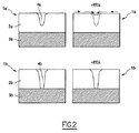
図2は、それぞれ埋め込み酸化物層3a、3b、およびその上のシリコン層2a、2bから構成される、SOI構造1a、1b(支持基板は図示せず)に対するRTA操作の影響を示す。
FIG. 2 shows the effect of RTA operation on
SOI構造1aのシリコン層2aは、深さがシリコン層2aの厚さよりも小さく、したがって埋め込み酸化物層3aの表面まで下方に延びない表層ホールを呈する。
The silicon layer 2a of the SOI structure 1a has a depth smaller than the thickness of the silicon layer 2a, and thus exhibits a surface layer hole that does not extend downward to the surface of the buried
これに反して、SOI構造1bのシリコン層2bは、シリコン層2bの厚さを貫通して、埋め込み酸化物層3bの表面まで下方に延びる致命ホール4bを呈する。
On the other hand, the silicon layer 2b of the
RTA操作は、表層ホール(表層ホール4aなど)の深さを大幅に(少なくとも1/2〜1/3に)低減するのに役立つ平滑化効果を有する。確かに、構造1aに関して図2の右側に概略的に示されるように、特に拡散と再結晶によってこれらのホールを止めることができる。
The RTA operation has a smoothing effect that helps to significantly reduce (at least 1/2 to 1/3) the depth of surface layer holes (such as
しかしRTA操作は、RTAの前に、薄層を貫通して(このケースでは埋め込み酸化物層3aの表面まで下方に)延びる致命ホール(ホール4bなど)に対しては効果がない。構造1bに関して図2の右側に概略的に示されるように、致命ホールはRTA操作では救済されない。
However, the RTA operation has no effect on critical holes (
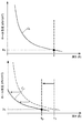
図3は、RTA操作の前(上側のグラフ)および後(下側のグラフ)のSOI層内のホール密度を表す。RTA操作の前では、厚さTのSOI層は、曲線Cbによって示される密度において、様々な深さの表層ホールを呈し、これはこれらのホールの深さに依存する。SOI層はまた、密度Dkの致命ホールを呈する。 FIG. 3 represents the hole density in the SOI layer before (upper graph) and after (lower graph) the RTA operation. Prior to RTA operation, the T-thick SOI layer exhibits various depths of surface holes at the density indicated by curve Cb, depending on the depth of these holes. The SOI layer also exhibits fatal holes of density Dk.
上述のように、RTA操作は致命ホールには効果がない。したがって致命ホール密度は変わらず、Dkに等しいままである。 As described above, the RTA operation has no effect on the critical hole. Therefore, the critical hole density remains unchanged and remains equal to Dk.
しかしRTA操作は、深さを減少し、さらには停止させることによって、表層ホールを救済するのに役立つ。RTA操作の結果、SOI層は、曲線Caで示されるように、密度が大幅に低減された表層ホールを呈する。 However, the RTA operation helps to relieve surface holes by reducing the depth and even stopping. As a result of the RTA operation, the SOI layer exhibits surface layer holes with a greatly reduced density, as shown by the curve Ca.
図4は、埋め込み酸化物層7と、その上のシリコン層6から構成される、SOI構造5に対するPOL操作の影響を示す。シリコン層6は、POL操作の前では表層ホール8を呈する。この図で明らかなように、シリコン層6のxオングストロームを除去し、それによって薄くなったシリコン層6’が得られ、表層ホール8の深さは低減される。
FIG. 4 shows the effect of the POL operation on the SOI structure 5 composed of the buried
さらに、POL操作によって除去されるシリコン層6の厚さ(表層ホール深さよりも重要である)は、POL操作によって前記表層ホールが除去されるように調節することができる。
Furthermore, the thickness of the
しかし、シリコン層が、埋め込み酸化物層まで下方に延びる致命ホールを呈する場合は、前記シリコン層は研磨後に依然として致命ホールを呈することが分かる。 However, it can be seen that when the silicon layer exhibits a critical hole extending down to the buried oxide layer, the silicon layer still exhibits a critical hole after polishing.
図5は、POL操作の前(上側のグラフ)および後(下側のグラフ)のSOI層内のホール密度を表す。POL操作の前では、厚さTbのSOI層は、曲線Cbによって示される密度において、様々な深さの表層ホールを呈し、これはこれらのホールの深さに依存する。SOI層はまた、密度Dkの致命ホールを呈する。 FIG. 5 represents the hole density in the SOI layer before (upper graph) and after (lower graph) the POL operation. Prior to the POL operation, the SOI layer of thickness Tb exhibits various depths of surface holes at the density indicated by curve Cb, depending on the depth of these holes. The SOI layer also exhibits fatal holes of density Dk.
上述のように、POL操作は致命ホールには効果がない。したがって致命ホール密度は変わらず、Dkに等しいままである。 As described above, the POL operation has no effect on the dead hole. Therefore, the critical hole density remains unchanged and remains equal to Dk.
しかしPOL操作は、深さを減少し、さらには停止させることによって、表層ホールを救済するのに役立つ。POL操作の結果、SOI層は、曲線Cp(これは曲線Cbと同一であるが、POLによる厚さの消耗により、深さ軸に沿ってシフトされる)で示されるように、密度が大幅に低減された表層ホールを呈する。 However, the POL operation helps to relieve surface holes by reducing the depth and even stopping. As a result of the POL operation, the SOI layer has a significantly higher density as shown by the curve Cp (which is the same as the curve Cb but shifted along the depth axis due to the consumption of thickness by the POL). Presents reduced surface layer holes.
図6は、埋め込み酸化物層11と、その上のシリコン層10から構成される、SOI構造9に対するSOx操作の影響を示す。シリコン層10は、SOx操作の前では表層ホール12を呈する。この図で明らかなように、SOx操作はホールの形状を再現し、その深さは変化しない。
FIG. 6 shows the effect of the SOx operation on the SOI structure 9 composed of the buried
図示されるように、始めに存在する表層ホール12の深さが顕著な場合は、SOx操作の後に、このホールが、埋め込み酸化物層まで下方に延び得る(致命ホール12’)。
As shown, if the depth of the
図7は、SOx操作の前(上側のグラフ)および後(下側のグラフ)のSOI層内のホール密度を表す。SOx操作の前では、厚さTiのSOI層は、曲線Cbによって示される密度において、様々な深さの表層ホールを呈し、これはこれらのホールの深さに依存する。SOI層はまた、密度Diの致命ホールを呈する。 FIG. 7 represents the hole density in the SOI layer before (upper graph) and after (lower graph) the SOx operation. Before the SOx operation, the SOI layer of thickness Ti exhibits various depths of surface holes at the density indicated by curve Cb, depending on the depth of these holes. The SOI layer also exhibits dead holes of density Di.
上述のように、SOx操作はホールの形状を再現し、その深さは変化しない。したがって、変化していない曲線Cbによって示されるように、表層ホール密度は変化せず、それらの深さに依存する。 As described above, the SOx operation reproduces the shape of the hole and its depth does not change. Thus, as shown by the unchanged curve Cb, the surface hole density does not change and depends on their depth.
しかしSOx操作により、SOI層の厚さは減少する。新しい厚さTfは始めの厚さTiより小さいので、致命ホールの密度はDiからDfに増加する。 However, with the SOx operation, the thickness of the SOI layer decreases. Since the new thickness Tf is smaller than the initial thickness Ti, the density of critical holes increases from Di to Df.
図7から明らかなように、SOx操作は表層ホールを救済するには役立たず、かつ致命ホール密度は増加する(この増加は、消耗した厚さTi−Tfに直接関係する)。 As is apparent from FIG. 7, the SOx operation does not help to relieve surface holes and the fatal hole density increases (this increase is directly related to the consumed thickness Ti-Tf).
SOx操作に関しては、化学エッチング操作がホールの形状を再現し、その深さは変化しない。SOx操作に関してはさらには、このことにより、始めに顕著な表層ホールは、後で埋め込み酸化物層まで下方に延び、したがって致命ホールに「変化」する(言い換えれば、その結果致命ホール密度が増加する)。 As for the SOx operation, the chemical etching operation reproduces the shape of the hole and its depth does not change. In addition, for SOx operations, this initially causes the prominent surface holes to later extend down to the buried oxide layer and thus “change” to critical holes (in other words, the critical hole density increases as a result). ).
上述のように、第1のファミリの操作(RTAまたはPOL操作)の前に存在する致命ホールは、前記操作では救済されないことになる。 As described above, the critical hole existing before the first family operation (RTA or POL operation) is not relieved by the operation.
したがって、図8で明らかなように、RTA/SOxのシーケンスとSOx/RTAのシーケンスとでは影響が非常に異なる。 Therefore, as apparent from FIG. 8, the influence is very different between the RTA / SOx sequence and the SOx / RTA sequence.
SOx/RTAシーケンスの場合では、SOx操作により初期の表層ホール13が(移転後に)、致命ホール14に変化することがあり得る。致命ホール14は、後続のRTA操作では救済されない。
In the case of the SOx / RTA sequence, the
一方、RTA/SOxシーケンスの場合では、同じ初期の表層ホール13は、救済されることになる。確かに、RTA操作はその深さを減少させ(ホール15参照)、SOxはシリコン層を薄くする。したがって結果としての構造は、ほぼ一体的に停止されたホール15’を呈する。
On the other hand, in the case of the RTA / SOx sequence, the same initial
もちろん、移転後に薄層内に致命ホールがあれば、これらのホールは救済されず最終製品中に致命的欠陥として残ることになる。 Of course, if there are fatal holes in the thin layer after relocation, these holes will not be relieved and will remain as fatal defects in the final product.
上記の観察に基づいて、本発明による方法は、
−最終構造の薄層が到達すべき厚さを選択するステップと、
−最終構造の薄層内に観察される致命ホールの最大密度を選択するステップと、
−剥離後に得られる中間構造に対して行うべき、少なくとも1つの操作を含む仕上げシーケンスを選択するステップと
を行うことを提案する。
Based on the above observations, the method according to the invention
-Selecting the thickness that the thin layer of the final structure should reach;
-Selecting the maximum density of critical holes observed in a thin layer of the final structure;
Proposing to select a finishing sequence including at least one operation to be performed on the intermediate structure obtained after peeling.
一般に特定の仕上げシーケンスは、薄い移転層の品質を、(たとえば粗さを平滑化しそれにより正しい厚さの均一性を確保することによって)向上し、応用分野での使用に適したものにするために、剥離後の構造に対して用いられる。 In general, certain finishing sequences improve the quality of the thin transfer layer (eg by smoothing the roughness and thereby ensuring the correct thickness uniformity) and making it suitable for use in application fields In addition, it is used for the structure after peeling.
仕上げシーケンスは特に、支持基板上に移転されたドナー基板の一部(薄い移転層)を薄くし、それにより最終構造の薄層の厚さが前記選択された厚さに到達するように適合される。 The finishing sequence is specifically adapted to thin a portion of the donor substrate (the thin transfer layer) transferred onto the support substrate, so that the thickness of the thin layer of the final structure reaches the selected thickness. The
前記仕上げシーケンスは、上述の操作(TA、POL、SOx、化学エッチング)の少なくとも1つを含むことができ、非限定的な例として示される以下のシーケンスなど、これら操作の任意の組合せからなることができる。
−RTA−SOx
−複数のRTA−SOxシーケンスの繰返し(RTA−SOx−RTA−SOxなど)
−SOx−POL−SOx(およびこのシーケンスの繰返し)
−SOx−RTA−POL−SOx(およびこのシーケンスの繰返し)
−SOx−RTA(およびこのシーケンスの繰返し)
The finishing sequence can include at least one of the above operations (TA, POL, SOx, chemical etching) and consist of any combination of these operations, including the following sequences shown as non-limiting examples: Can do.
-RTA-SOx
-Repeating multiple RTA-SOx sequences (such as RTA-SOx-RTA-SOx)
-SOx-POL-SOx (and repetition of this sequence)
-SOx-RTA-POL-SOx (and repetition of this sequence)
-SOx-RTA (and repetition of this sequence)
上述のように、RTA操作(およびより一般に任意の平滑化アニール操作)は、表層ホールを停止させるのに役立つ。したがってこのようなRTA操作を含むシーケンスを利用することが有利である。 As mentioned above, the RTA operation (and more generally any smoothing anneal operation) helps to stop the surface holes. Therefore, it is advantageous to use a sequence including such an RTA operation.
さらに、特定の条件下では、RTA操作はSi層の下の酸化物層を密閉するのに役立ち、これは化学エッチングまたは犠牲酸化を行う前として望ましい場合がある(たとえば国際公開第2004/079801号パンフレットを参照)。 Furthermore, under certain conditions, the RTA operation helps to seal the oxide layer under the Si layer, which may be desirable before performing chemical etching or sacrificial oxidation (eg, WO 2004/079801). See brochure).
ただし特定のシーケンス中のこのような操作の、(残りの厚さに関する)位置が重要になり得る(たとえば米国特許公開第2004/0151483号を参照)。 However, the position (with respect to the remaining thickness) of such operations in a particular sequence can be important (see, eg, US Patent Publication No. 2004/0151483).
さらに、RTA操作は、材料の除去を実行するのに、および薄層を薄くするのには有効でない。 Furthermore, RTA operations are not effective in performing material removal and thinning thin layers.
これに反して、SOx操作は、薄層を薄くするのに有効であり、特に剥離後に損傷した領域を除去するのに、または最終構造の薄層の選択された厚さを得るのに有効である。 On the other hand, the SOx operation is effective for thinning the thin layer, especially for removing damaged areas after delamination or for obtaining a selected thickness of the thin layer of the final structure. is there.
SOx操作によって除去することができる厚さは、通常100〜1000オングストロームの間である。 The thickness that can be removed by the SOx operation is usually between 100 and 1000 angstroms.
ただしSOx操作は、致命ホール密度を増加し得るので注意深く行わなければならない。 However, the SOx operation must be carefully performed because it can increase the critical hole density.
したがって2つのSOx操作の間に、RTA操作を行うことが賢明である。 Therefore, it is advisable to perform an RTA operation between two SOx operations.
POL操作はまた、材料の除去によって薄層を薄くするのに役立つが、このような操作は厚さの均一性を低下させ、さらには薄層が損傷を受ける。したがってPOLは、できるだけ限定し、薄くするステップで薄層への損傷がより少ないステップ(SOxなど)の後、さらにはRTAの後に行わなければならない。 POL operations also help to thin the thin layer by removing material, but such operations reduce thickness uniformity and even damage the thin layer. Therefore, POL should be done as limited as possible, after steps that are less damaging to thin layers (such as SOx) and even after RTA.
POL操作は通常、材料の除去を200〜500オングストロームの間に制限する(それによって厚さ均一性の低下を制限するのに役立つ)ために、RTAと組み合わされる。 POL operations are typically combined with RTA to limit material removal between 200-500 angstroms (and thereby help limit thickness uniformity degradation).
本発明による方法はまた、支持基板上に移転すべきドナー基板の部分が、仕上げシーケンスの各操作後に、前記最大密度より低い致命ホールの密度を呈するように、かつ仕上げシーケンスを達成した後、前記選択された厚さに到達するように、前記部分の最小厚さを決定するステップを行うことを提案する。 The method according to the invention also provides that the portion of the donor substrate to be transferred onto the support substrate exhibits a density of critical holes lower than the maximum density after each operation of the finishing sequence, and after achieving the finishing sequence, It is proposed to perform the step of determining the minimum thickness of the part so as to reach a selected thickness.
したがって本発明は、支持基板上に移転すべき適正な厚さを選択し、
−最終構造の薄層が到達すべき選択された厚さを考慮に入れ、
−選択された仕上げ操作シーケンスを考慮に入れる(したがってこの仕上げシーケンスの各操作のホール密度への影響を考慮に入れる)
ことによって、最終構造の薄層内の致命ホールの密度を制限することを提案する。
Therefore, the present invention selects the appropriate thickness to be transferred onto the support substrate,
-Taking into account the selected thickness that the thin layer of the final structure should reach;
Take into account the selected finishing operation sequence (thus taking into account the effect of each finishing operation on the hole density)
It is proposed to limit the density of critical holes in the thin layer of the final structure.
上記で論じられたグラフ(図3、5、および7)は、各操作(それぞれRTA、POL、およびSOx)のホール密度に対する影響を示す。したがって、これらのグラフを組み合わせて、仕上げシーケンスの全部(これは特定の順序で行われる複数の操作を有することができ、選択された厚さに薄層を薄くするように適合される)のホール密度に対する影響を評価することができる。 The graphs discussed above (FIGS. 3, 5, and 7) show the effect on hole density for each operation (RTA, POL, and SOx, respectively). Thus, combining these graphs, the holes in the entire finishing sequence (which can have multiple operations performed in a specific order and are adapted to thin the lamina to a selected thickness) The effect on density can be evaluated.
したがって、このグラフの組合せから移転すべき適切な厚さを導き、それによって各操作後に、致命ホール密度が選択された最大致命ホール密度より低くなるようにすることができる。したがって、選択された最終厚さおよび致命ホールの最大密度から始めて、(仕上げシーケンスの操作を逆の順に取り上げ、最後のものから始めることにより)特定の操作の前に薄層が呈しなければならない最小厚さ、したがって最終的には、移転すべき厚さを決定することが可能である。 Therefore, an appropriate thickness to be transferred can be derived from this graph combination, so that after each operation, the critical hole density is lower than the selected maximum critical hole density. Thus, starting with the selected final thickness and maximum density of critical holes, the minimum that a thin layer must exhibit before a particular operation (by taking the finishing sequence operations in reverse order and starting with the last one) It is possible to determine the thickness, and ultimately the thickness to be transferred.
例示として図8の上側の図をとると、選択された仕上げシーケンスは、SOx操作と後続のRTA操作を含む。したがって図7と図3のグラフが組み合わされる。 Taking the top diagram of FIG. 8 as an illustration, the selected finishing sequence includes a SOx operation followed by an RTA operation. Therefore, the graphs of FIGS. 7 and 3 are combined.
移転すべき最小厚さTiは、薄層の厚さがSOx操作によって減少し(SOx操作後は、移転後のTiからTfに減少)、その結果致命ホール密度が増加することを考慮に入れなければならない。 The minimum thickness Ti to be transferred must be taken into account that the thickness of the thin layer is reduced by the SOx operation (after the SOx operation, it decreases from Ti after the transfer to Tf), resulting in an increase in the critical hole density. I must.
選択された最大密度が、致命ホール0.3個/cm2に設定されたと考えよう。そうすると移転すべき最小厚さTiは、SOx操作後、すなわちRTA操作(これは致命ホール密度には影響を及ぼさないが表層ホール密度の低減に役立つ)前の厚さTfが、0.3個/cm2の致命ホール密度が見られる厚さより大(すなわち1000オングストロームより大)となるように選ばなければならない。 Consider that the selected maximum density is set to 0.3 critical holes / cm 2 . Then, the minimum thickness Ti to be transferred is 0.3 pieces / thickness Tf after the SOx operation, that is, before the RTA operation (which does not affect the critical hole density but helps to reduce the surface hole density). The critical hole density of cm 2 must be chosen to be greater than the thickness seen (ie greater than 1000 angstroms).
次に図8の下側のグラフを参照すると、今度は選択された仕上げシーケンスは、RTA操作と後続のSOx操作を含む。したがって図3と図7のグラフが組み合わされる。この場合最初の操作では、薄層の厚さは減少しないがホール密度が変化し、後続のSOx操作によって(多くの)新しい致命ホールが生成し易くならないようになる(図7に示されるようなSOx操作であるが、図3の下側のグラフの曲線Caで示されるようなRTA操作後の低減されたホール密度から開始する)。 Referring now to the lower graph of FIG. 8, the selected finishing sequence now includes an RTA operation followed by a SOx operation. Therefore, the graphs of FIGS. 3 and 7 are combined. In this case, in the first operation, the thickness of the thin layer does not decrease, but the hole density changes, and subsequent SOx operations do not facilitate the generation of (many) new dead holes (as shown in FIG. 7). SOx operation, but starting with reduced hole density after RTA operation as shown by curve Ca in the lower graph of FIG. 3).
したがって、選択された最終厚さと選択された致命ホールの最大密度に対して、RTA−SOx仕上げシーケンスの場合の移転すべき最小厚さは、SOx−RTA仕上げシーケンスの場合の移転すべき最小厚さとは異なることが分かる。 Thus, for the selected final thickness and the selected maximum density of critical holes, the minimum thickness to be transferred in the case of the RTA-SOx finishing sequence is the minimum thickness to be transferred in the case of the SOx-RTA finishing sequence. Is different.
もちろん脆化領域は、ドナー基板の厚さ内に、前記決定された移転すべき最小厚さとほぼ等しいかそれより大きい深さに生成される。 Of course, the embrittlement region is created within the thickness of the donor substrate to a depth approximately equal to or greater than the determined minimum thickness to be transferred.
可能な実施形態によれば、脆化領域は、そこから薄層が作製されなければならないドナー基板の面の下に、化学種を注入することによって生成される。 According to a possible embodiment, the embrittled region is created by implanting chemical species beneath the surface of the donor substrate from which a thin layer must be made.
このような注入は、単一の化学種(水素など)を注入することにより、または少なくとも2つの異なる化学種(ヘリウムと水素の共注入など)を注入することによって行うことができる。 Such implantation can be done by injecting a single species (such as hydrogen) or by implanting at least two different species (such as co-implantation of helium and hydrogen).
本発明の好ましい実施形態によれば、注入条件は、注入エネルギーが15KeV〜120KeVの間、より好ましくは15KeV〜80KeVの間からなるように選択される。 According to a preferred embodiment of the invention, the implantation conditions are selected such that the implantation energy is comprised between 15 KeV and 120 KeV, more preferably between 15 KeV and 80 KeV.
好ましい実施形態によれば、仕上げシーケンスは、前記第1の操作ファミリからの少なくとも1つの操作、すなわち表層ホールの深さ低減を可能にし薄層内のホール密度を変化させるのに役立つ操作を含む(図3および図5の、RTAおよびPOL操作の影響を参照されたい)。 According to a preferred embodiment, the finishing sequence comprises at least one operation from said first operating family, i.e. an operation that allows a reduction in the depth of the surface holes and serves to change the hole density in the thin layer ( (See the effects of RTA and POL operations in FIGS. 3 and 5).
前記表層ホール深さ低減操作は、たとえばTA操作、またはPOL操作である。 The surface hole depth reduction operation is, for example, a TA operation or a POL operation.
本発明の有利な実施形態によれば、仕上げシーケンスは、前記第1の操作ファミリからの複数の操作、すなわちそれぞれが表層ホールの深さ低減を可能にする複数の操作を含む。この有利な実施形態は、それにより残留表層ホールの深さが低減され、さらにはこれらの表層ホールを完全に除去するのに役立ち得るので、さらなる利益が得られる。 According to an advantageous embodiment of the invention, the finishing sequence comprises a plurality of operations from said first operating family, i.e. a plurality of operations each enabling a depth reduction of the surface hole. This advantageous embodiment provides additional benefits because it reduces the depth of residual surface holes and can help to completely remove these surface holes.
図9は、仕上げシーケンスがSOx/RTA/POL/SOx操作シーケンスである本発明による方法の可能な実施形態によって得られる改善を示す。選択された到達すべき厚さと選択された致命ホールの最大密度を考慮に入れて、これらの操作のそれぞれの後で、薄い移転層が前記選択された密度より低い致命ホールの密度を呈するように、移転すべき最小厚さを決定するために、図7、3、5、そして7のグラフが組み合わされる。 FIG. 9 shows the improvement obtained by a possible embodiment of the method according to the invention in which the finishing sequence is a SOx / RTA / POL / SOx operating sequence. Taking into account the selected reachable thickness and the maximum density of selected critical holes, after each of these operations, the thin transfer layer exhibits a density of critical holes lower than the selected density. The graphs of FIGS. 7, 3, 5, and 7 are combined to determine the minimum thickness to be transferred.
上側の図では、注入ステップが従来法により実行され、厚さtの層がドナー基板上に移転される。 In the upper diagram, the implantation step is performed by conventional methods and a layer of thickness t is transferred onto the donor substrate.
下側の図では、注入ステップが本発明により実行され、厚さt+500オングストロームの層がドナー基板上に移転される。 In the lower figure, an implantation step is performed according to the present invention and a layer t + 500 angstroms thick is transferred onto the donor substrate.
従来法の場合は、最初のSOx操作は表層ホールを救済せず、さらには埋め込み酸化物層まで下方に延びる致命ホール(ホール16など)の形成をもたらす。 In the case of the conventional method, the first SOx operation does not relieve the surface layer hole, and further results in the formation of a critical hole (such as hole 16) that extends down to the buried oxide layer.
これらの致命ホールは、後続のRTA操作によっても、また後続のPOL操作によっても救済されない。最後のSOx操作は、致命ホール18を有するSOI構造をもたらし、したがってその応用分野では受け入れられない。 These critical holes are not rescued by subsequent RTA operations or by subsequent POL operations. The last SOx operation results in an SOI structure with a deadly hole 18 and is therefore unacceptable for its application.
これに反して、本発明の可能な実施形態による方法の場合、移転層は、最初のSOx操作によって致命ホールが、(選択された最大密度を超える過度に顕著な密度で)形成されないように十分厚い。 On the other hand, in the case of the method according to a possible embodiment of the invention, the transfer layer is sufficient to ensure that dead holes are not formed (at an overly significant density above the selected maximum density) by the first SOx operation. Thick.
したがって、この場合は、後続のRTA操作(すなわちホール19などの表層ホールの深さ低減を可能にする操作)が、特にそれらの深さを低減することによって(ホール19’参照)、存在する表層ホールを救済するのに役立つ。このRTA操作は、致命ホール密度には影響を及ぼさないので、この操作後に、致命ホール密度は依然として選択された最大密度を超えない。 Thus, in this case, subsequent RTA operations (ie operations that allow a reduction in the depth of surface holes such as hole 19), in particular by reducing their depth (see hole 19 '), are present in the surface layer. Help rescue the hole. Since this RTA operation does not affect the critical hole density, after this operation, the critical hole density still does not exceed the selected maximum density.
POL操作により、この操作によって除去される薄層の厚さ内に含まれるこれらの表層ホール(この場合、ホール19’など、pオングストロームより浅いホール)が、除去されることになる。POL操作により、この操作の前にpオングストロームより深かった表層ホールは、深さが低減されることになる。RTA操作に関しては、POL操作は致命ホール密度に影響を及ぼさない。 The POL operation will remove those surface layer holes (in this case holes shallower than p angstroms, such as hole 19 ') that fall within the thickness of the thin layer removed by this operation. Due to the POL operation, the depth of surface layer holes deeper than p angstroms prior to this operation will be reduced. For RTA operations, POL operations do not affect the critical hole density.
最終的に、最後の操作(第2のSOx操作)の終了時に、所望の厚さ、および最小化されたホールの密度、ならびに特に、より少ない表層ホールと前記選択された最大密度より低い致命ホール密度を呈する薄層が得られる。 Finally, at the end of the last operation (second SOx operation), the desired thickness and minimized hole density, and in particular, fewer surface holes and critical holes lower than the selected maximum density A thin layer exhibiting density is obtained.
この第2のSOx操作により、従来法によって得られる薄層20と同様な厚さの、最終薄層21を得るように適合された犠牲酸化が実行されることに留意されなければならない。
It has to be noted that this second SOx operation performs a sacrificial oxidation adapted to obtain the final
したがって、この第2のSOx操作により、移転層の厚さの増加(この場合は+500オングストローム)を補償するように適合された、より重要な犠牲酸化が実行される。 Therefore, this second SOx operation performs a more important sacrificial oxidation adapted to compensate for the transfer layer thickness increase (in this case +500 angstroms).
さらに、先の例は、RTA操作(またはより一般的に言えば表層ホールの深さ低減を可能にする操作)は、致命ホールを呈さない(または少なくとも最大密度より低い密度の致命ホールを呈する)薄層上に行われるので、致命ホールの密度に関して利益が達せられることを示している。 Furthermore, the previous example shows that RTA operations (or more generally, operations that allow surface hole depth reduction) do not exhibit fatal holes (or at least present dead holes with a density lower than the maximum density). Since it is done on a thin layer, it shows that a profit can be achieved regarding the density of critical holes.
さらに、前記操作前の致命ホール密度は、特に支持基板上に移転される層の厚さを増加することによって適切に行われる注入ステップにより、制御される。 Furthermore, the critical hole density before the operation is controlled by an injection step that is suitably performed, in particular by increasing the thickness of the layer transferred onto the support substrate.
図10は、移転層の450オングストロームの増加を示し、RTA/SOx/RTA/SOxの仕上げ操作シーケンスと組み合わされた場合、最終薄層(厚さ200オングストローム)内で、致命ホールの密度を1/5に低減することが可能になる。確かに、従来法により得られたSOI構造について描かれた左側の図は0.5ホール/cm2の致命ホール密度を示し、上述のようにして得られたSOI構造について描かれた右側の図はわずか0.1ホール/cm2の致命ホール密度を示している。 FIG. 10 shows an increase of 450 Å in the transfer layer, and when combined with the finishing operation sequence of RTA / SOx / RTA / SOx, the density of critical holes in the final thin layer (thickness 200 Å) is reduced to 1 /. It becomes possible to reduce to 5. Certainly, the diagram on the left drawn for the SOI structure obtained by the conventional method shows a critical hole density of 0.5 holes / cm 2 , and the diagram on the right drawn for the SOI structure obtained as described above. Indicates a lethal hole density of only 0.1 holes / cm 2 .
図11は、本発明の可能な実施形態による、SOIデバイスを製造するための方法を示す流れ図である。 FIG. 11 is a flow diagram illustrating a method for manufacturing an SOI device, according to a possible embodiment of the present invention.
ブロック10では、特に、
−最終構造の薄層の厚さTf
−移転後に得られる中間構造の、仕上げ操作シーケンス(この場合はRTA/SOx/RTA/SOxシーケンス)
−最終構造の薄層内の致命ホールの最大密度DM
を選択することにより、最終SOI製品の仕様が列挙されている。
In
The thickness Tf of the thin layer of the final structure
-Finishing operation sequence of intermediate structure obtained after transfer (in this case RTA / SOx / RTA / SOx sequence)
-Maximum density D M of critical holes in the thin layer of the final structure
The final SOI product specifications are listed by selecting.
ブロック20では、移転すべき厚さが選択される。
At
ブロック30では、支持基板上に移転されたドナー基板の部分内の致命ホールの密度が、選択された最大密度DMより高いかどうかが確認される。
In
肯定なら、移転すべき厚さは増加され(ブロック40)、その後ブロック30が繰り返される。 If yes, the thickness to be transferred is increased (block 40) and then block 30 is repeated.
否定なら、仕上げシーケンスの最初の操作が行われる。この場合はブロック50でRTA操作が行われる。すでに上述されたように、このようなRTA操作は致命ホールには効果がないが、表層ホールの深さ低減に役立つ。
If not, the first operation in the finishing sequence is performed. In this case, an RTA operation is performed at
ブロック60では、仕上げシーケンスの第2の操作、SOx操作が行われる。上述のように、このようなSOx操作は、移転された薄層を薄くするのに有効であるが、厚さの消耗に応じて致命ホール密度が増加する。
In
ブロック70では、SOx操作に続き、ブロック30と同様に、支持基板上に移転されたドナー基板の部分内の致命ホールの密度が、選択された最大密度DMより高いかどうかが確認される。
In
肯定なら、ブロック80で、SOx操作(ブロック60で行われる)の厚さの消耗を小さくできるかどうかが確認される。これは、選択された特定の仕上げシーケンス、および選択された最終厚さTfを考慮に入れてなされる。 If yes, block 80 checks to see if the thickness consumption of the SOx operation (performed at block 60) can be reduced. This is done taking into account the specific finishing sequence selected and the final thickness Tf selected.
厚さの消耗を小さくできる場合は、この新たに設定された操作条件に従って、SOx操作が行われる(ブロック60)。 If the thickness consumption can be reduced, the SOx operation is performed in accordance with the newly set operation condition (block 60).
厚さの消耗を小さくできない場合は、次いでブロック40(すなわち移転される厚さの増加)が行われる。 If the thickness wear cannot be reduced, then block 40 (i.e., increase in transferred thickness) is performed.
ブロック70に戻り、SOx操作後の致命ホールの密度が、最大密度DMより低い場合は、仕上げシーケンスの次の操作(ここでは、厚さが消耗せず致命ホール密度が変化しないRTA操作)がブロック90で行われる。
Returning to block 70, the density of the critical hole after SOx operation is lower than the maximum density D M, the following operations of the finishing sequence (here, fatal hole density without wasting thickness does not change RTA operation) This is done at
その後、ブロック100でSOx操作が行われる。ブロック110と120では、それぞれブロック70と80で行われたのと同様の操作が行われる。SOx操作に続き、致命ホール密度が最大密度DMより低いことを条件(ブロック110)として、(ブロック10で定義された)仕様に適合する最終SOI製品がブロック130で得られる。
Thereafter, a SOx operation is performed at
もちろん、図11の流れ図は、単に例示的なものであり、本発明は、説明され示された実施形態には全く限定されることなく、当業者なら多くの代替形態または変更形態を提示することができるであろう。 Of course, the flow diagram of FIG. 11 is merely exemplary, and the present invention is not limited in any way to the embodiments described and shown, and those skilled in the art will present many alternatives or modifications. Will be able to.
Claims (18)
前記ドナー基板を、支持基板に密着して配置するステップと、
前記ドナー基板の一部を前記支持基板上に移転するために、前記ドナー基板を前記脆化領域の高さで剥離し、それによって中間構造を形成するステップと
を含む、基板上の半導体材料の薄層を備える最終構造を製造する方法において、
前記最終構造の前記薄層が到達すべき厚さを選択するステップと、
前記最終構造の前記薄層内に観察される致命ホールの最大密度を選択するステップと、
剥離後に得られる前記中間構造に対して行うべき、少なくとも1つの操作を含む仕上げシーケンスを選択するステップと、
前記支持基板上に移転すべき前記ドナー基板の前記部分が、
前記仕上げシーケンスの各操作後に、前記最大密度より低い致命ホールの密度を呈するように、かつ、
前記仕上げシーケンスを達成した後、前記選択された厚さに到達するように、
前記部分の最小厚さを決定するステップと
をさらに含むことを特徴とする方法。 Creating an embrittled region in the thickness of the donor substrate;
Placing the donor substrate in intimate contact with a support substrate;
Peeling the donor substrate at the height of the embrittlement region to transfer a portion of the donor substrate onto the support substrate, thereby forming an intermediate structure of a semiconductor material on the substrate In a method of manufacturing a final structure comprising a thin layer,
Selecting the thickness that the thin layer of the final structure should reach;
Selecting the maximum density of critical holes observed in the thin layer of the final structure;
Selecting a finishing sequence including at least one operation to be performed on the intermediate structure obtained after peeling;
The portion of the donor substrate to be transferred onto the support substrate is
So as to exhibit a density of critical holes lower than the maximum density after each operation of the finishing sequence; and
After achieving the finishing sequence, to reach the selected thickness,
Determining the minimum thickness of the portion.
前記仕上げシーケンスの各操作後に、前記最大密度より低い致命ホールの密度を呈するように、かつ、
前記仕上げシーケンスの全部が達成された後に、前記選択された厚さに到達するように
移転すべき最小厚さが決定されることを特徴とする方法。 A method for determining the thickness of a portion of a donor substrate to be transferred onto a support substrate, wherein the portion is subsequently subjected to a selected finishing sequence comprising at least one operation. Part is
So as to exhibit a density of critical holes lower than the maximum density after each operation of the finishing sequence; and
A method wherein a minimum thickness to be transferred is determined to reach the selected thickness after all of the finishing sequence has been achieved.
Applications Claiming Priority (1)
| Application Number | Priority Date | Filing Date | Title |
|---|---|---|---|
| PCT/IB2004/004390 WO2006070220A1 (en) | 2004-12-28 | 2004-12-28 | Method for obtaining a thin layer having a low density of holes |
Related Child Applications (1)
| Application Number | Title | Priority Date | Filing Date |
|---|---|---|---|
| JP2012135100A Division JP5096634B2 (en) | 2012-06-14 | 2012-06-14 | Method for obtaining thin layers with low hole density |
Publications (1)
| Publication Number | Publication Date |
|---|---|
| JP2008526010A true JP2008526010A (en) | 2008-07-17 |
Family
ID=34960268
Family Applications (1)
| Application Number | Title | Priority Date | Filing Date |
|---|---|---|---|
| JP2007547685A Pending JP2008526010A (en) | 2004-12-28 | 2004-12-28 | Method for obtaining thin layers with low hole density |
Country Status (7)
| Country | Link |
|---|---|
| US (1) | US7485545B2 (en) |
| EP (1) | EP1831922B9 (en) |
| JP (1) | JP2008526010A (en) |
| CN (1) | CN100550342C (en) |
| AT (1) | ATE441206T1 (en) |
| DE (1) | DE602004022882D1 (en) |
| WO (1) | WO2006070220A1 (en) |
Cited By (8)
| Publication number | Priority date | Publication date | Assignee | Title |
|---|---|---|---|---|
| JP2008021992A (en) * | 2006-07-13 | 2008-01-31 | Soitec Silicon On Insulator Technologies | Heat treatment for bonding interface stabilization |
| JP2009032972A (en) * | 2007-07-27 | 2009-02-12 | Shin Etsu Handotai Co Ltd | Method of manufacturing bonded wafer |
| JP2010062532A (en) * | 2008-09-03 | 2010-03-18 | Soitec Silicon On Insulator Technologies | Method for fabricating semiconductor on insulator substrate with reduced secco defect density |
| JP2012520579A (en) * | 2009-03-18 | 2012-09-06 | ソイテック | Surface treatment method for "silicon-on-insulator" SOI type substrates |
| JP2012222294A (en) * | 2011-04-13 | 2012-11-12 | Shin Etsu Handotai Co Ltd | Method for manufacturing laminated wafer |
| WO2013102968A1 (en) | 2012-01-06 | 2013-07-11 | 信越半導体株式会社 | Method for manufacturing bonded silicon-on-insulator (soi) wafer |
| WO2013111242A1 (en) * | 2012-01-24 | 2013-08-01 | 信越半導体株式会社 | Bonded soi wafer manufacturing method |
| JP2016082093A (en) * | 2014-10-17 | 2016-05-16 | 信越半導体株式会社 | Bonded wafer manufacturing method |
Citations (6)
| Publication number | Priority date | Publication date | Assignee | Title |
|---|---|---|---|---|
| JPH1084100A (en) * | 1996-09-06 | 1998-03-31 | Shin Etsu Handotai Co Ltd | Manufacture of soi substrate |
| JPH11307472A (en) * | 1998-04-23 | 1999-11-05 | Shin Etsu Handotai Co Ltd | Soi wafer and manufacture soi by hydrogen ion releasing method |
| JP2003509838A (en) * | 1999-08-20 | 2003-03-11 | エス オー イ テク シリコン オン インシュレータ テクノロジース | Microelectronics substrate processing method and substrate obtained by the method |
| JP2003510799A (en) * | 1999-08-20 | 2003-03-18 | エス オー イ テク シリコン オン インシュレータ テクノロジース | Microelectronics substrate processing method and substrate obtained by the method |
| JP2004259970A (en) * | 2003-02-26 | 2004-09-16 | Shin Etsu Handotai Co Ltd | Soi wafer and method for manufacturing it |
| JP2004535685A (en) * | 2001-07-16 | 2004-11-25 | エス.オー.アイ.テック、シリコン、オン、インシュレター、テクノロジーズ | How to improve the surface condition |
Family Cites Families (16)
| Publication number | Priority date | Publication date | Assignee | Title |
|---|---|---|---|---|
| FR2681472B1 (en) * | 1991-09-18 | 1993-10-29 | Commissariat Energie Atomique | PROCESS FOR PRODUCING THIN FILMS OF SEMICONDUCTOR MATERIAL. |
| SG67458A1 (en) * | 1996-12-18 | 1999-09-21 | Canon Kk | Process for producing semiconductor article |
| US6162705A (en) * | 1997-05-12 | 2000-12-19 | Silicon Genesis Corporation | Controlled cleavage process and resulting device using beta annealing |
| FR2777115B1 (en) * | 1998-04-07 | 2001-07-13 | Commissariat Energie Atomique | PROCESS FOR TREATING SEMICONDUCTOR SUBSTRATES AND STRUCTURES OBTAINED BY THIS PROCESS |
| JP2002110688A (en) * | 2000-09-29 | 2002-04-12 | Canon Inc | Thermal processing method of soi, and its manufacturing method |
| FR2894990B1 (en) * | 2005-12-21 | 2008-02-22 | Soitec Silicon On Insulator | PROCESS FOR PRODUCING SUBSTRATES, IN PARTICULAR FOR OPTICS, ELECTRONICS OR OPTOELECTRONICS AND SUBSTRATE OBTAINED BY SAID PROCESS |
| JP4304879B2 (en) * | 2001-04-06 | 2009-07-29 | 信越半導体株式会社 | Method for determining the implantation amount of hydrogen ions or rare gas ions |
| WO2003046993A1 (en) * | 2001-11-29 | 2003-06-05 | Shin-Etsu Handotai Co.,Ltd. | Production method for soi wafer |
| FR2846786B1 (en) * | 2002-11-05 | 2005-06-17 | PROCESS FOR QUICK THERMAL RECOVERY OF CROWN WAFERS | |
| FR2852143B1 (en) | 2003-03-04 | 2005-10-14 | Soitec Silicon On Insulator | PROCESS FOR THE PREVENTIVE TREATMENT OF THE CROWN OF A MULTILAYER SLICE |
| FR2855908B1 (en) * | 2003-06-06 | 2005-08-26 | Soitec Silicon On Insulator | METHOD FOR OBTAINING A STRUCTURE COMPRISING AT LEAST ONE SUBSTRATE AND AN ULTRAMINO LAYER |
| EP1652230A2 (en) | 2003-07-29 | 2006-05-03 | S.O.I.Tec Silicon on Insulator Technologies | Method for obtaining a thin high-quality layer by co-implantation and thermal annealing |
| FR2858461B1 (en) * | 2003-07-30 | 2005-11-04 | Soitec Silicon On Insulator | IMPLEMENTING A STRUCTURE COMPRISING A PROTECTIVE LAYER AGAINST CHEMICAL TREATMENTS |
| FR2860249B1 (en) * | 2003-09-30 | 2005-12-09 | Michel Bruel | METHOD FOR MANUFACTURING PLATE-LIKE STRUCTURE, ESPECIALLY SILICON, PROCESS APPLICATION, AND PLATE-LIKE STRUCTURE, PARTICULARLY SILICON |
| FR2861497B1 (en) | 2003-10-28 | 2006-02-10 | Soitec Silicon On Insulator | METHOD FOR CATASTROPHIC TRANSFER OF A FINE LAYER AFTER CO-IMPLANTATION |
| US7772087B2 (en) * | 2003-12-19 | 2010-08-10 | Commissariat A L'energie Atomique | Method of catastrophic transfer of a thin film after co-implantation |
-
2004
- 2004-12-28 DE DE602004022882T patent/DE602004022882D1/en active Active
- 2004-12-28 EP EP04806549A patent/EP1831922B9/en active Active
- 2004-12-28 CN CNB2004800447452A patent/CN100550342C/en active Active
- 2004-12-28 JP JP2007547685A patent/JP2008526010A/en active Pending
- 2004-12-28 WO PCT/IB2004/004390 patent/WO2006070220A1/en active Application Filing
- 2004-12-28 AT AT04806549T patent/ATE441206T1/en not_active IP Right Cessation
-
2006
- 2006-01-10 US US11/328,061 patent/US7485545B2/en active Active
Patent Citations (6)
| Publication number | Priority date | Publication date | Assignee | Title |
|---|---|---|---|---|
| JPH1084100A (en) * | 1996-09-06 | 1998-03-31 | Shin Etsu Handotai Co Ltd | Manufacture of soi substrate |
| JPH11307472A (en) * | 1998-04-23 | 1999-11-05 | Shin Etsu Handotai Co Ltd | Soi wafer and manufacture soi by hydrogen ion releasing method |
| JP2003509838A (en) * | 1999-08-20 | 2003-03-11 | エス オー イ テク シリコン オン インシュレータ テクノロジース | Microelectronics substrate processing method and substrate obtained by the method |
| JP2003510799A (en) * | 1999-08-20 | 2003-03-18 | エス オー イ テク シリコン オン インシュレータ テクノロジース | Microelectronics substrate processing method and substrate obtained by the method |
| JP2004535685A (en) * | 2001-07-16 | 2004-11-25 | エス.オー.アイ.テック、シリコン、オン、インシュレター、テクノロジーズ | How to improve the surface condition |
| JP2004259970A (en) * | 2003-02-26 | 2004-09-16 | Shin Etsu Handotai Co Ltd | Soi wafer and method for manufacturing it |
Cited By (13)
| Publication number | Priority date | Publication date | Assignee | Title |
|---|---|---|---|---|
| US8461018B2 (en) | 2006-07-13 | 2013-06-11 | S.O.I.Tec Silicon On Insulator Technologies | Treatment for bonding interface stabilization |
| US8216916B2 (en) | 2006-07-13 | 2012-07-10 | S.O.I. Tec Silicon On Insulator Technologies | Treatment for bonding interface stabilization |
| JP2008021992A (en) * | 2006-07-13 | 2008-01-31 | Soitec Silicon On Insulator Technologies | Heat treatment for bonding interface stabilization |
| JP2009032972A (en) * | 2007-07-27 | 2009-02-12 | Shin Etsu Handotai Co Ltd | Method of manufacturing bonded wafer |
| JP2010062532A (en) * | 2008-09-03 | 2010-03-18 | Soitec Silicon On Insulator Technologies | Method for fabricating semiconductor on insulator substrate with reduced secco defect density |
| KR101623968B1 (en) | 2008-09-03 | 2016-05-24 | 소이텍 | Method for fabricating a semiconductor on insulator substrate with reduced SECCO defect density |
| JP2012520579A (en) * | 2009-03-18 | 2012-09-06 | ソイテック | Surface treatment method for "silicon-on-insulator" SOI type substrates |
| JP2012222294A (en) * | 2011-04-13 | 2012-11-12 | Shin Etsu Handotai Co Ltd | Method for manufacturing laminated wafer |
| WO2013102968A1 (en) | 2012-01-06 | 2013-07-11 | 信越半導体株式会社 | Method for manufacturing bonded silicon-on-insulator (soi) wafer |
| US9076840B2 (en) | 2012-01-06 | 2015-07-07 | Shin-Etsu Handotai Co., Ltd. | Method for manufacturing a bonded SOI wafer |
| WO2013111242A1 (en) * | 2012-01-24 | 2013-08-01 | 信越半導体株式会社 | Bonded soi wafer manufacturing method |
| US9093497B2 (en) | 2012-01-24 | 2015-07-28 | Shin-Etsu Handotai Co., Ltd. | Method for manufacturing bonded SOI wafer |
| JP2016082093A (en) * | 2014-10-17 | 2016-05-16 | 信越半導体株式会社 | Bonded wafer manufacturing method |
Also Published As
| Publication number | Publication date |
|---|---|
| ATE441206T1 (en) | 2009-09-15 |
| EP1831922A1 (en) | 2007-09-12 |
| CN101091242A (en) | 2007-12-19 |
| DE602004022882D1 (en) | 2009-10-08 |
| US20060141755A1 (en) | 2006-06-29 |
| CN100550342C (en) | 2009-10-14 |
| EP1831922B9 (en) | 2010-02-24 |
| WO2006070220A1 (en) | 2006-07-06 |
| US7485545B2 (en) | 2009-02-03 |
| EP1831922B1 (en) | 2009-08-26 |
Similar Documents
| Publication | Publication Date | Title |
|---|---|---|
| JP5042837B2 (en) | Thin layer transfer method that performs co-injection process under conditions that avoid the formation of bubbles and limit roughness | |
| US7276428B2 (en) | Methods for forming a semiconductor structure | |
| KR101134485B1 (en) | Method for obtaining a thin layer by implementing co-implantation and subsequent implantation | |
| KR101353970B1 (en) | Method for transferring a monocrystalline semiconductor layer onto a support substrate | |
| US7282449B2 (en) | Thermal treatment of a semiconductor layer | |
| JP2007201429A (en) | Manufacturing method of composite substrate | |
| US7485545B2 (en) | Method of configuring a process to obtain a thin layer with a low density of holes | |
| JP2008021992A (en) | Heat treatment for bonding interface stabilization | |
| KR101623968B1 (en) | Method for fabricating a semiconductor on insulator substrate with reduced SECCO defect density | |
| JP5646593B2 (en) | Surface treatment method for "silicon-on-insulator" SOI type substrates | |
| JP2007500435A (en) | A method for obtaining thin layers with improved properties by co-implantation and thermal annealing. | |
| US8324072B2 (en) | Process for locally dissolving the oxide layer in a semiconductor-on-insulator type structure | |
| JP4987470B2 (en) | Method for producing ultrathin layer thinned by inducing self-supporting | |
| JP4285244B2 (en) | Manufacturing method of SOI wafer | |
| JP5096634B2 (en) | Method for obtaining thin layers with low hole density | |
| JP4762547B2 (en) | Manufacturing method of multilayer structure | |
| KR100914898B1 (en) | Method for obtaining a thin layer having a low density of holes | |
| TW202345408A (en) | Method for manufacturing a 3d circuit with mutualised steps of recrystallising and activating dopants |
Legal Events
| Date | Code | Title | Description |
|---|---|---|---|
| A977 | Report on retrieval |
Free format text: JAPANESE INTERMEDIATE CODE: A971007 Effective date: 20110414 |
|
| A131 | Notification of reasons for refusal |
Free format text: JAPANESE INTERMEDIATE CODE: A131 Effective date: 20110426 |
|
| A521 | Request for written amendment filed |
Free format text: JAPANESE INTERMEDIATE CODE: A523 Effective date: 20110726 |
|
| A02 | Decision of refusal |
Free format text: JAPANESE INTERMEDIATE CODE: A02 Effective date: 20120228 |
|
| A521 | Request for written amendment filed |
Free format text: JAPANESE INTERMEDIATE CODE: A523 Effective date: 20120614 |
|
| A911 | Transfer to examiner for re-examination before appeal (zenchi) |
Free format text: JAPANESE INTERMEDIATE CODE: A911 Effective date: 20120621 |
|
| A912 | Re-examination (zenchi) completed and case transferred to appeal board |
Free format text: JAPANESE INTERMEDIATE CODE: A912 Effective date: 20120727 |