JP2008520316A - Hybrid IC for ultrasonic beam former probe - Google Patents
Hybrid IC for ultrasonic beam former probe Download PDFInfo
- Publication number
- JP2008520316A JP2008520316A JP2007542429A JP2007542429A JP2008520316A JP 2008520316 A JP2008520316 A JP 2008520316A JP 2007542429 A JP2007542429 A JP 2007542429A JP 2007542429 A JP2007542429 A JP 2007542429A JP 2008520316 A JP2008520316 A JP 2008520316A
- Authority
- JP
- Japan
- Prior art keywords
- circuit
- integrated circuit
- voltage integrated
- substrate
- package
- Prior art date
- Legal status (The legal status is an assumption and is not a legal conclusion. Google has not performed a legal analysis and makes no representation as to the accuracy of the status listed.)
- Pending
Links
Images


Classifications
-
- A—HUMAN NECESSITIES
- A61—MEDICAL OR VETERINARY SCIENCE; HYGIENE
- A61B—DIAGNOSIS; SURGERY; IDENTIFICATION
- A61B8/00—Diagnosis using ultrasonic, sonic or infrasonic waves
- A61B8/54—Control of the diagnostic device
- A61B8/546—Control of the diagnostic device involving monitoring or regulation of device temperature
-
- G—PHYSICS
- G01—MEASURING; TESTING
- G01S—RADIO DIRECTION-FINDING; RADIO NAVIGATION; DETERMINING DISTANCE OR VELOCITY BY USE OF RADIO WAVES; LOCATING OR PRESENCE-DETECTING BY USE OF THE REFLECTION OR RERADIATION OF RADIO WAVES; ANALOGOUS ARRANGEMENTS USING OTHER WAVES
- G01S15/00—Systems using the reflection or reradiation of acoustic waves, e.g. sonar systems
- G01S15/88—Sonar systems specially adapted for specific applications
- G01S15/89—Sonar systems specially adapted for specific applications for mapping or imaging
- G01S15/8906—Short-range imaging systems; Acoustic microscope systems using pulse-echo techniques
- G01S15/8909—Short-range imaging systems; Acoustic microscope systems using pulse-echo techniques using a static transducer configuration
- G01S15/8915—Short-range imaging systems; Acoustic microscope systems using pulse-echo techniques using a static transducer configuration using a transducer array
- G01S15/8927—Short-range imaging systems; Acoustic microscope systems using pulse-echo techniques using a static transducer configuration using a transducer array using simultaneously or sequentially two or more subarrays or subapertures
-
- G—PHYSICS
- G01—MEASURING; TESTING
- G01S—RADIO DIRECTION-FINDING; RADIO NAVIGATION; DETERMINING DISTANCE OR VELOCITY BY USE OF RADIO WAVES; LOCATING OR PRESENCE-DETECTING BY USE OF THE REFLECTION OR RERADIATION OF RADIO WAVES; ANALOGOUS ARRANGEMENTS USING OTHER WAVES
- G01S7/00—Details of systems according to groups G01S13/00, G01S15/00, G01S17/00
- G01S7/52—Details of systems according to groups G01S13/00, G01S15/00, G01S17/00 of systems according to group G01S15/00
- G01S7/52017—Details of systems according to groups G01S13/00, G01S15/00, G01S17/00 of systems according to group G01S15/00 particularly adapted to short-range imaging
- G01S7/52079—Constructional features
- G01S7/5208—Constructional features with integration of processing functions inside probe or scanhead
-
- G—PHYSICS
- G01—MEASURING; TESTING
- G01S—RADIO DIRECTION-FINDING; RADIO NAVIGATION; DETERMINING DISTANCE OR VELOCITY BY USE OF RADIO WAVES; LOCATING OR PRESENCE-DETECTING BY USE OF THE REFLECTION OR RERADIATION OF RADIO WAVES; ANALOGOUS ARRANGEMENTS USING OTHER WAVES
- G01S7/00—Details of systems according to groups G01S13/00, G01S15/00, G01S17/00
- G01S7/52—Details of systems according to groups G01S13/00, G01S15/00, G01S17/00 of systems according to group G01S15/00
- G01S7/523—Details of pulse systems
-
- G—PHYSICS
- G10—MUSICAL INSTRUMENTS; ACOUSTICS
- G10K—SOUND-PRODUCING DEVICES; METHODS OR DEVICES FOR PROTECTING AGAINST, OR FOR DAMPING, NOISE OR OTHER ACOUSTIC WAVES IN GENERAL; ACOUSTICS NOT OTHERWISE PROVIDED FOR
- G10K11/00—Methods or devices for transmitting, conducting or directing sound in general; Methods or devices for protecting against, or for damping, noise or other acoustic waves in general
- G10K11/18—Methods or devices for transmitting, conducting or directing sound
- G10K11/26—Sound-focusing or directing, e.g. scanning
- G10K11/34—Sound-focusing or directing, e.g. scanning using electrical steering of transducer arrays, e.g. beam steering
- G10K11/341—Circuits therefor
- G10K11/346—Circuits therefor using phase variation
Abstract
超音波プローブにおけるマイクロビームフォーマのためのハイブリッド集積回路パッケージが、基板と、送信ビームを発生させるためにプローブの変換器素子に送信されるべき送信パルスを生成するためのドライバと、時間遅延回路及び加算回路を含み、前記時間遅延回路は、前記変換器素子からの複数の反射パルスを受信すると共に前記反射パルスを遅延させるために動作し、前記加算回路は、ビーム形成信号を発生させるために前記遅延させられた反射パルスのグループを加算するために動作する、ビームフォーマ回路とを含む。ドライバ回路は、前記ドライバ回路を含む高電圧集積回路デバイスの部分になる。前記ビームフォーマ回路の少なくとも一つの部分は、低電圧集積回路デバイスの部分になり、前記高電圧集積回路デバイス及び前記低電圧集積回路デバイスは前記基板上に実装される。
A hybrid integrated circuit package for a microbeamformer in an ultrasonic probe includes a substrate, a driver for generating transmit pulses to be transmitted to a transducer element of the probe to generate a transmit beam, a time delay circuit, and An adder circuit, wherein the time delay circuit receives a plurality of reflected pulses from the transducer element and operates to delay the reflected pulses, and the adder circuit generates the beamforming signal to generate a beam forming signal. A beamformer circuit that operates to add the group of delayed reflected pulses. The driver circuit becomes part of a high voltage integrated circuit device that includes the driver circuit. At least one portion of the beamformer circuit becomes a portion of a low voltage integrated circuit device, and the high voltage integrated circuit device and the low voltage integrated circuit device are mounted on the substrate.
Description
本発明は、変換器素子インタフェースの高電圧要求仕様と、制御及びビーム形成(フォーミング)機能の高密度機能要求仕様との両方をもたらす超音波ビームフォーマプローブのためのハイブリッド集積回路(IC)に関する。 The present invention relates to a hybrid integrated circuit (IC) for an ultrasonic beamformer probe that provides both the high voltage requirements of the transducer element interface and the high density functional requirements of the control and beamforming functions.
医療用超音波画像化システムは、リアルタイムに人体の内部構造を非侵襲的に見るために使用される。超音波画像化システムは、超音波パルスを送信すると共に受信するための変換器(トランスデューサ)のアレイを含んでいる。各々の変換器は圧電素子になる。送信ビームフォーマ回路は、送信ビームを作るために特定のタイミングシーケンスで変換器のアレイにおける各々の変換器に電気パルスを加える(もたらす)。送信ビームは、異なる音響(アコースティック)特性を有する組織構造体によって反射される。反射されたビームは、受信変換器によって、ディスプレイにより表されてもよい画像信号に変換される電気パルスに変換される。各々の変換器は、送信変換器と受信変換器との両方として動作してもよい。 Medical ultrasound imaging systems are used to non-invasively view the internal structure of the human body in real time. An ultrasound imaging system includes an array of transducers for transmitting and receiving ultrasound pulses. Each transducer becomes a piezoelectric element. The transmit beamformer circuit applies (provides) electrical pulses to each transducer in the transducer array in a specific timing sequence to create a transmit beam. The transmitted beam is reflected by tissue structures having different acoustic (acoustic) properties. The reflected beam is converted by the receiving transducer into electrical pulses that are converted into an image signal that may be represented by a display. Each converter may operate as both a transmitting converter and a receiving converter.
高解像度を実現するため、変換器アレイは、数百乃至数千の変換器素子を含むように製作される。変換器は、変換器からの多くの信号を、超音波プロセッサステーション(局)における更なるビームフォーマ(形成器)によって管理され得る複数の信号に変換するマイクロビームフォーマ電子機器に接続される。ケーブルによって変換器から超音波処理ステーションに全ての信号を送信することは困難であるため、マイクロビームフォーマ電子機器は、変換器を備えるプローブにおいて構成されることが必要とされる。 To achieve high resolution, the transducer array is fabricated to include hundreds to thousands of transducer elements. The transducer is connected to microbeamformer electronics that converts many signals from the transducer into multiple signals that can be managed by a further beamformer at the ultrasound processor station. Since it is difficult to transmit all signals from the transducer to the sonication station by cable, the microbeamformer electronics are required to be configured in a probe with a transducer.
プローブにおける回路は、送信ビームのためのドライバを動作させるために十分な電圧及び電力をもたらすことが必要とされると共に、同時にプローブにおける熱発生を制限しなければならない。プローブは通常、60-200Vp-pを必要とし、より新しいプローブは当該範囲の下限にもたらされる。送信パルスから受信器を接続及び切断するように素子(要素)及びスイッチをパルシングするためのドライバは当該電圧を発生させることが必要とされる。しかしながら、制御及びビーム形成機能部は、変換器からの多くの信号を処理するために高密度の集積を必要とする。高電圧を提供するICデバイスは、物理的に大きくなり、より多くのエネルギを消費し、それ故により多くの熱を発生させる。しかしながら、高密度を提供するICデバイスは、動作電圧を制限する。 Circuitry at the probe is required to provide sufficient voltage and power to operate the driver for the transmit beam and at the same time limit heat generation at the probe. Probes usually require 60-200V pp , and newer probes are brought to the lower end of the range. Drivers for pulsing elements and switches to connect and disconnect the receiver from the transmitted pulse are required to generate the voltage. However, the control and beamforming function requires high density integration to process many signals from the transducer. IC devices that provide high voltages become physically larger, consume more energy, and therefore generate more heat. However, IC devices that provide high density limit the operating voltage.
本発明の目的は、マイクロビームフォーマ超音波プローブのための高電圧要求仕様と高密度要求仕様との両方を満たすハイブリッドICを提供することにある。 An object of the present invention is to provide a hybrid IC that satisfies both high voltage requirement specifications and high density requirement specifications for a microbeamformer ultrasonic probe.
本発明の目的は、超音波プローブにおけるマイクロビームフォーマのためのハイブリッド集積回路パッケージによって満たされ、超音波プローブは、パルスを送信すると共に受信する変換器素子のアレイを有する。回路パッケージは、基板と、送信ビームを発生させるために変換器素子に送信されるべき送信パルスを生成するためのドライバを含む高電圧集積回路デバイスと、変換器素子から反射パルスを受信すると共に反射パルスを遅延させるための時間遅延回路を含む低電圧集積回路デバイスと、ビーム形成(された)信号を発生させるために遅延させられた反射パルスのグループを加算する加算(総和)回路とを含む。高電圧集積回路デバイスは、反射パルスから送信パルスを絶縁分離するためのスイッチ及び受信器ゲインを実現するための増幅器を含んでいてもよい。 The object of the present invention is met by a hybrid integrated circuit package for a microbeamformer in an ultrasonic probe, which has an array of transducer elements that transmit and receive pulses. The circuit package includes a substrate, a high voltage integrated circuit device including a driver for generating a transmit pulse to be transmitted to the transducer element to generate a transmit beam, and receives and reflects the reflected pulse from the transducer element. A low voltage integrated circuit device that includes a time delay circuit for delaying the pulses, and an adder (summing) circuit that adds the group of reflected pulses delayed to generate a beamformed signal. The high voltage integrated circuit device may include a switch for isolating the transmitted pulse from the reflected pulse and an amplifier for realizing the receiver gain.
高電圧集積回路がCMOS又はBiCMOSであってもよく、低電圧集積回路は、相補型金属酸化膜半導体(complementary metal oxide semiconductors (CMOS))を有する。 The high voltage integrated circuit may be CMOS or BiCMOS, and the low voltage integrated circuit has complementary metal oxide semiconductors (CMOS).
いくつかの場合において、変換器素子のアレイが前記基板に直接接続されてもよい。 In some cases, an array of transducer elements may be directly connected to the substrate.
基板は、リジッド(剛性)であってもよく、フレキシブル(弾性)であってもよい。更に、基板がフレックス材料に接続されるリジッドコンポーネントを有していてもよい。 The substrate may be rigid (rigid) or flexible (elastic). Furthermore, the substrate may have a rigid component connected to the flex material.
高電圧集積回路デバイス及び低電圧集積回路デバイスが、ボールグリッドアレイ(ball grid array)を使用して基板に接続されてもよい。 High voltage integrated circuit devices and low voltage integrated circuit devices may be connected to the substrate using a ball grid array.
更に、高電圧集積回路デバイス、低電圧集積回路デバイス、及び基板が、スタックされた(積み重ねられた)構成で接続されてもよい。 Further, the high voltage integrated circuit device, the low voltage integrated circuit device, and the substrate may be connected in a stacked configuration.
本発明の他の目的及び特徴は、添付図面に関連して検討される以下の詳細な説明から明らかになるであろう。しかしながら、図面は単に説明のためだけに描かれており、従属請求項が参照されるべき本発明の限定の明確化として描かれているわけではないことは理解されるべきである。図面は必ずしも寸法通りに描かれているではなく、示されていない限り、図面は、ここに記載されている構造体及びプロシージャを概念的に描くことのみが意図されていることは更に留意されるべきである。 Other objects and features of the present invention will become apparent from the following detailed description considered in conjunction with the accompanying drawings. It should be understood, however, that the drawings are drawn merely for purposes of explanation and that the dependent claims are not drawn as a clarification of the limitations of the invention to which reference should be made. It is further noted that the drawings are not necessarily drawn to scale, and that unless otherwise indicated, the drawings are only intended to conceptually depict the structures and procedures described herein. Should.
図面において、同じ参照特徴は、いくつかの図を通して同じ要素を示している。 In the drawings, like reference features indicate like elements throughout the several views.
図1は、変換器110を含む超音波プローブ100のブロック図である。送信回路120は、被験体(サブジェクト)において送信ビームを発生させるための変換器110にもたらされる電気パルスを発生させるためのプローブ100において構成される。送信回路120は、必要とされるとき、送信パルスを集束させるために時間遅延をもたらすビームフォーマ回路130から受信される信号に応答して電気パルスを発生させる。ビームフォーマ回路130は、変換器110から反射パルスを受信するために構成される。ビームフォーマ回路130が、反射ビームの出力レベルをセットするために時間遅延及び/又はゲイン(利得)制御をもたらしてもよい。送信/受信(T/R)スイッチ120は、反射パルスから送信パルスを絶縁分離するためのビームフォーマ回路130、送信回路120、及び変換器110に接続される。好ましい実施例において、超音波プローブ110は、3次元画像化を可能にするために何千もの変換器を有するマイクロビームフォーマ超音波プローブになる。代わりに、超音波プローブが、高度2D(2次元)画像をもたらすために、広がる仰角(エレベーション)アパーチャ(expanding elevation aperture)を有する1xD型プローブを有していてもよい。これらの1xD型プローブは、1.125D, 1.25D,..... 1.75Dプローブとも称される。ここで数は、使用される集束法の種類を示している。
FIG. 1 is a block diagram of an
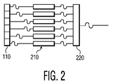
図2は、反射信号を処理するためのビームフォーマの概念を示す簡略化された概略図である。ビームフォーマ130は、時間遅延回路210及び信号加算回路220を含む。上述のように、時間遅延回路210が、送信パルスを集束するために使用されてもよい。一つ又は複数の送信パルスがもたらされた後、各々の変換器110は、反射パルスを受信すると共に反射パルスに基づいて信号を生成する。時間遅延回路210が、時間遅延を反射パルス信号にもたらしてもよく、反射パルス信号はそれから、形成ビーム(formed beam)を発生させるために加算回路220において加算される。図2は、簡単化のために、一つの形成ビームを形成するための六つの変換器を示している。プローブ100が何千もの変換器を有していてもよく、ビームフォーマ130が、変換器からのこれら何千もの信号を、更なるビーム形成のために超音波プロセッサに送信される何百もの信号にまで低減してもよい。この種のプローブは、米国特許第6,491,634号公報及び米国特許第6,013,032号公報において開示されており、全内容は参照によってここに明確に組み入れられる。
FIG. 2 is a simplified schematic diagram illustrating the concept of a beamformer for processing reflected signals. The beam former 130 includes a
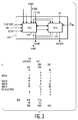
図3は、低電圧集積回路(LVIC)310及び高電圧集積回路(HVIC)320並びに以下に記載される様々な信号のためのピンの数のリストを示す概略図である。多くの変換器を有するマイクロビームフォーマプローブは、何千もの変換器信号を管理するために高密度集積回路を必要とする。同時に、変換器への送信パルスを生成するためにドライバに対して高電圧が必要とされる。必要とされる電圧レベルをもたらすHVICは通常、マイクロビームフォーマのために必要とされる密度を有していない。更に、これらのHVICは、熱を発生する多くのエネルギを使用する。超音波プローブは生成され得る熱の量を制限する基準内で動作しなければならないため、熱の発生は超音波プローブにとって有害である。本発明によれば、ハイブリッド集積回路パッケージは、送信パルスを生成するために必要とされる高電圧と、変換器からの反射パルスを管理するために必要とされる密度との両方をもたらすためにLVIC 310及びHVIC 320を含む。HVIC 320は、送信回路120をもたらし、更にスイッチ140も含む。LVIC 310はビームフォーマ130を含む。信号ELは、変換器素子に対する接続部を表す。アナログ信号は、T/Rスイッチを通じてLVICに送信される、変換器からの信号になる。
HV及びRTNは、パルスを発生させるためにHVICに高電圧信号をもたらす。SUM信号は、外部超音波プロセッサに送信されるビームフォーマの出力になる。VDDA, VCORE, 及びVDDDは電圧供給接続部である。GNDD及びGNDAはグランド(接地)接続部である。CTRL線は、送信パルス及び反射パルスのためのディレイ(遅延)及びバイアシング機能を制御する制御線である。
FIG. 3 is a schematic diagram showing a list of low voltage integrated circuit (LVIC) 310 and high voltage integrated circuit (HVIC) 320 and the number of pins for the various signals described below. Microbeamformer probes with many transducers require high density integrated circuits to manage thousands of transducer signals. At the same time, a high voltage is required for the driver to generate a transmission pulse to the converter. HVICs that provide the required voltage levels typically do not have the density required for microbeamformers. In addition, these HVICs use a lot of energy that generates heat. The generation of heat is detrimental to the ultrasound probe because the ultrasound probe must operate within criteria that limit the amount of heat that can be generated. In accordance with the present invention, the hybrid integrated circuit package provides both the high voltage required to generate the transmit pulse and the density required to manage the reflected pulse from the transducer. Includes LVIC 310 and HVIC 320. The HVIC 320 provides the
HV and RTN provide a high voltage signal to the HVIC to generate pulses. The SUM signal becomes the output of the beamformer that is sent to the external ultrasound processor. VDDA, VCORE, and VDDD are voltage supply connections. GNDD and GNDA are ground (ground) connections. The CTRL line is a control line that controls the delay and biasing functions for the transmitted and reflected pulses.
好ましい実施例において、図1に示されている回路はアナログ回路である。目下、本技術の制限はプローブ内のディジタル信号への変換の包含を回避する。しかしながら将来、ビームフォーマ回路130は、反射パルスから受信される信号が、時間遅延されると共に加算される前にアナログからディジタル信号に変換されるA/Dコンバータを含むディジタル回路も有することは可能である。
In the preferred embodiment, the circuit shown in FIG. 1 is an analog circuit. Currently, the limitations of the present technology avoid the inclusion of conversion to digital signals within the probe. In the future, however, the
一つの実施例において、LVIC 310は、CMOS技術を使用して製作され、HVIC 320は、バイポーラ又は電界効果トランジスタ技術を使用して製造される。CMOS技術は現在好ましいが、LVIC 310が、代わりに、フィールドプログラマブルゲートアレイ(Field Programmable Gate Arrays (FPGA))を使用して製造されてもよい。
In one embodiment,
図4は、一つの変換器素子に対して送信すると共に受信するためのLVIC 310及びHVIC 320の単一のチャネルを示す。LVIC 310は、遅延線、ドライバ312、及びプリアンプ313を有するRAM 311を含む。HVIC 320は、修正演算トランスコンダクタンス増幅器(Operational Transconductance Amplifier (OTA))322を含んでおり、反射パルスを増幅するための増幅器313aを含んでいてもよい。本願の場合のOTAに対する修正は、ユーザが高調波歪のために消費電力を交換することを可能にするためのバイアス調整と、受信モードにおいて電力を低減するディスエーブル機能と、固定ゲイン低雑音増幅器と、送信/受信スイッチへの接続部とを含んでいる。好ましい実施例はOTA 322を使用しているが、他の種類の増幅器が使用されてもよい。
FIG. 4 shows a single channel of
送信モードにおいて、遅延線311はスイッチ315を介して反転され、遅延線311のコンデンサはプリチャージ(前充電)される。HV増幅器322は、スイッチ326によってRAMに接続され、HV送信/受信スイッチ324は開放され(オープンになり)、高電圧がLVIC 310に印加されることは阻止される。このモードにおいて、HV増幅器322からのパルスは負荷、すなわち変換器素子ELにもたらされる。
In the transmission mode, the
受信モードにおいて、遅延線311は入力を受信する。スイッチ326は、HV増幅器322をRAM 311から切断するために開放(オープン)になる。HV送信/受信スイッチ324は閉じられ、HV増幅器322からのパルスに応答して変換器素子において生成される信号がLVIC 310の遅延線311に伝えられることは可能になる。遅延信号はそれから、更なる処理のための加算器(summer)に送信される。
In the reception mode, the
LVIC 310及びHVIC 320が、現在知られている、又は従来から引き続き知られているいかなるハイブリッドIC構成体で構成されてもよい。限定しない例によって、図5乃至9bは、使用されてもよい様々な例示の構成体を示す。しかしながら、これらの例は、異なるプロセス技術を使用して製作される、二つ又はそれより多くの相互接続されたICを含むハイブリッドICパッケージを生成するために使用されてもよい様々な技術を決して限定するものではない。図5は、相互接続のための高密度基板410上に構成されるLVIC 310 及びHVIC 320を示す。このような構成体は、マルチパッケージモジュール(Multi Package Module (MPM))と称される。基板媒体は、好ましくは、フリップチップとワイヤボンド接続部との両方を可能にする。しかしながら、接続部が、専らフリップチップ又はワイヤボンド接続部であってもよい。図5に示されているように、基板410が、標準的な(スタンダード)ボールグリッドアレイ420に入れられてもよい。基板構成体上のこのようなチップは、例えばAmkor Technology, Inc. Chandler AZによって使用されている。
The
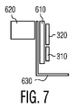
図6は、LVIC 310 及びHVIC 320が基板510に接続される他の実施例を示す。更に、変換器110を含むセンサ520は基板510にも接続される。図6は、フレキシブルコネクタ(flexible connector)530が、プローブから超音波プロセッサに信号を伝えるために基板に接続されてもよいことも示す。図7は、センサ620がフレキシブルコネクタ630に直接接続され、基板610がフレキシブルセンサ630に接続される更なる他の実施例を示す。図7の実施例において、基板はLVIC 310及び HVIC 320に接続される。図8に示されている更なる構成体において、LVIC 310, HVIC 320, 及びセンサ520はそれぞれフレキシブル基板710に接続される。この実施例において、接続部は、マイクロボールグリッドアレイを使用して製作されてもよい。フレキシブル接続材料は、例えばDyconex AG, Bassersdorf, Switzerland及びTessera, Inc., San Jose, CA.によって製造される。
FIG. 6 shows another embodiment in which
図9a及び9bは、スタックされたダイの概念がハイブリッドICを組み立てるために使用されてもよいことを示している。示されている実施例において、LVIC 310及び HVIC 320は、マイクロボールグリッドアレイ基板810において構成される。LVIC 310及び HVIC 320のスタッキングは、相互接続部が側面めっき(サイドプレーティング)によって制作されるIrving Sensors, Inc., Costa Mesa, CAによるネオスタッキング(neo-stacking)技術を使用して実現されてもよい。代わりに、相互接続部が、ChipPAK, Inc., Koreaによるボンドワイヤを使用してパッケージレベルでもたらされてもよい。
Figures 9a and 9b show that the stacked die concept may be used to assemble a hybrid IC. In the embodiment shown,
本発明の好ましい実施例に適用される本発明の基本的な新規特徴が示され、記載され、指摘されているが、記載のデバイスの形態及び詳細並びにその動作における様々な省略、代替、及び変形が、本発明の保護範囲から逸脱することなく当業者によってなされることは理解されるであろう。例えば、同じ結果を実現するようにほぼ同じ方法でほぼ同じ機能を実行する要素の全ての組み合わせが本発明の範囲内にあることは明らかに意図される。更に、本発明の実施例又はいかなる開示形態にも関して記載の、及び/又は示されている構造体及び/又は要素が、全設計選択事項としていかなる他の開示、記載、若しくは提案形態又は実施例において含まれてもよいことは認識されるべきである。それ故に、従属請求項の範囲によって示されるようにのみ限定されるべきであることが意図される。 Although the basic novel features of the present invention as applied to preferred embodiments of the present invention are shown, described and pointed out, various omissions, alternatives and variations in the form and details of the described devices and their operation are shown. However, it will be understood by those skilled in the art without departing from the protection scope of the present invention. For example, it is clearly contemplated that all combinations of elements that perform substantially the same function in substantially the same way to achieve the same result are within the scope of the invention. Further, the structures and / or elements described and / or illustrated with respect to the embodiments of the present invention or any disclosed form may be used as a total design choice for any other disclosure, description, or proposed form or implementation. It should be appreciated that it may be included in the examples. It is therefore intended that the invention should be limited only as indicated by the scope of the dependent claims.
Claims (12)
基板と、
送信ビームを発生させるために前記変換器素子に送信されるべき集束された送信パルスを生成するためのドライバ回路と、
時間遅延回路及び加算回路を含み、前記時間遅延回路は、前記変換器素子からの複数の反射パルスを受信すると共に前記反射パルスを遅延させるために動作し、前記加算回路は、ビーム形成信号を発生させるために前記遅延させられた反射パルスのグループを加算するために動作する、ビームフォーマ回路と、
前記ドライバ回路を含む高電圧集積回路デバイスと、
前記ビームフォーマ回路の少なくとも一つの部分を含む低電圧集積回路デバイスと
を有し、前記高電圧集積回路及び前記低電圧集積回路は前記基板上に実装されるハイブリッド集積回路パッケージ。 A hybrid integrated circuit package for a microbeamformer in an ultrasonic probe, the ultrasonic probe having an array of transducer elements for transmitting and receiving pulses, the circuit package comprising:
A substrate,
A driver circuit for generating a focused transmit pulse to be transmitted to the transducer element to generate a transmit beam;
A time delay circuit and an adder circuit, wherein the time delay circuit receives a plurality of reflected pulses from the transducer element and operates to delay the reflected pulses, and the adder circuit generates a beam forming signal A beamformer circuit operable to add the group of delayed reflected pulses to cause
A high voltage integrated circuit device comprising the driver circuit;
A hybrid integrated circuit package comprising: a low voltage integrated circuit device including at least one portion of the beamformer circuit, wherein the high voltage integrated circuit and the low voltage integrated circuit are mounted on the substrate.
Applications Claiming Priority (2)
| Application Number | Priority Date | Filing Date | Title |
|---|---|---|---|
| US63009004P | 2004-11-22 | 2004-11-22 | |
| PCT/IB2005/053803 WO2006054260A1 (en) | 2004-11-22 | 2005-11-17 | Hybrid ic for ultrasound beamformer probe |
Publications (2)
| Publication Number | Publication Date |
|---|---|
| JP2008520316A true JP2008520316A (en) | 2008-06-19 |
| JP2008520316A5 JP2008520316A5 (en) | 2009-01-15 |
Family
ID=35842025
Family Applications (1)
| Application Number | Title | Priority Date | Filing Date |
|---|---|---|---|
| JP2007542429A Pending JP2008520316A (en) | 2004-11-22 | 2005-11-17 | Hybrid IC for ultrasonic beam former probe |
Country Status (5)
| Country | Link |
|---|---|
| US (1) | US20090146695A1 (en) |
| EP (1) | EP1817609A1 (en) |
| JP (1) | JP2008520316A (en) |
| CN (1) | CN101061392A (en) |
| WO (1) | WO2006054260A1 (en) |
Cited By (7)
| Publication number | Priority date | Publication date | Assignee | Title |
|---|---|---|---|---|
| JP2011078755A (en) * | 2009-09-20 | 2011-04-21 | General Electric Co <Ge> | Large area modular sensor array assembly and method for making the same |
| JP2012505696A (en) * | 2008-10-20 | 2012-03-08 | コーニンクレッカ フィリップス エレクトロニクス エヌ ヴィ | Low voltage ultrasound system with high voltage transducer |
| JP2012508054A (en) * | 2008-11-11 | 2012-04-05 | コーニンクレッカ フィリップス エレクトロニクス エヌ ヴィ | Configurable microbeamformer circuit for ultrasound diagnostic imaging system |
| JP2017511247A (en) * | 2014-04-18 | 2017-04-20 | バタフライ ネットワーク,インコーポレイテッド | Structure of single substrate ultrasonic imaging apparatus, related apparatus and method |
| US20170326589A1 (en) * | 2014-12-15 | 2017-11-16 | Koninklijke Philips N.V. | Compact ultrasound transducer with direct coax attachment |
| US10856847B2 (en) | 2013-03-15 | 2020-12-08 | Butterfly Network, Inc. | Monolithic ultrasonic imaging devices, systems and methods |
| JP2021508584A (en) * | 2018-01-02 | 2021-03-11 | コーニンクレッカ フィリップス エヌ ヴェKoninklijke Philips N.V. | High Power Micro Beam Former Ultrasonic Transducer Probe |
Families Citing this family (11)
| Publication number | Priority date | Publication date | Assignee | Title |
|---|---|---|---|---|
| EP2070114B1 (en) * | 2006-09-25 | 2010-01-06 | Koninklijke Philips Electronics N.V. | Flip-chip interconnection through chip vias |
| US7687976B2 (en) | 2007-01-31 | 2010-03-30 | General Electric Company | Ultrasound imaging system |
| US7892176B2 (en) | 2007-05-02 | 2011-02-22 | General Electric Company | Monitoring or imaging system with interconnect structure for large area sensor array |
| US8717654B2 (en) * | 2009-05-15 | 2014-05-06 | Koninklijke Philips N.V. | Optical probe with feedback correction |
| JP5689697B2 (en) * | 2011-01-27 | 2015-03-25 | 株式会社東芝 | Ultrasonic probe and ultrasonic diagnostic apparatus |
| US9439625B2 (en) * | 2013-02-28 | 2016-09-13 | General Electric Company | Delta delay approach for ultrasound beamforming on an ASIC |
| US10828671B2 (en) * | 2013-06-26 | 2020-11-10 | Koninklijke Philips N.V. | Integrated circuit arrangement for a hexagonal CMUT ultrasound transducer array with offset columns |
| WO2016006739A1 (en) * | 2014-07-10 | 2016-01-14 | 삼성전자주식회사 | Ultrasound probe and ultrasound imaging device |
| CN109642942B (en) * | 2016-09-02 | 2023-06-13 | 皇家飞利浦有限公司 | Ultrasound probe with low frequency, low voltage digital microbeamformer |
| KR101925144B1 (en) * | 2017-01-12 | 2019-02-27 | 삼성메디슨 주식회사 | Ultrasound probe, ultrasound imaging apparatus and method for controlling thereof |
| DE102017217214B3 (en) * | 2017-09-27 | 2018-11-08 | Karlsruher Institut für Technologie | Apparatus for driving and reading a group of ultrasonic transducers for ultrasonic computed tomography and ultrasound computed tomography |
Citations (3)
| Publication number | Priority date | Publication date | Assignee | Title |
|---|---|---|---|---|
| JP2004041730A (en) * | 2002-06-27 | 2004-02-12 | Siemens Medical Solutions Usa Inc | Multi-dimensional transducer array for ultrasonic imaging and its manufacturing method |
| JP2004274721A (en) * | 2003-03-06 | 2004-09-30 | General Electric Co <Ge> | Integrated high-voltage switching circuit for ultrasonic transducer array |
| WO2004091812A2 (en) * | 2003-04-15 | 2004-10-28 | Koninklijke Philips Electronics N.V. | Two-dimensional (2d) array capable of harmonic generation for ultrasound imaging |
Family Cites Families (9)
| Publication number | Priority date | Publication date | Assignee | Title |
|---|---|---|---|---|
| US5744898A (en) * | 1992-05-14 | 1998-04-28 | Duke University | Ultrasound transducer array with transmitter/receiver integrated circuitry |
| US6043032A (en) * | 1993-09-22 | 2000-03-28 | Tosoh Corporation | Method of extracting nucleic acids and method of detecting specified nucleic acid sequences |
| US5906580A (en) * | 1997-05-05 | 1999-05-25 | Creare Inc. | Ultrasound system and method of administering ultrasound including a plurality of multi-layer transducer elements |
| US5997479A (en) * | 1998-05-28 | 1999-12-07 | Hewlett-Packard Company | Phased array acoustic systems with intra-group processors |
| US6117085A (en) * | 1998-11-20 | 2000-09-12 | Atl Ultrasound, Inc. | Ultrasonic diagnostic imaging system with cordless scanhead charger |
| US6142946A (en) * | 1998-11-20 | 2000-11-07 | Atl Ultrasound, Inc. | Ultrasonic diagnostic imaging system with cordless scanheads |
| US6380766B2 (en) * | 1999-03-19 | 2002-04-30 | Bernard J Savord | Integrated circuitry for use with transducer elements in an imaging system |
| US6969352B2 (en) * | 1999-06-22 | 2005-11-29 | Teratech Corporation | Ultrasound probe with integrated electronics |
| US6491634B1 (en) * | 2000-10-13 | 2002-12-10 | Koninklijke Philips Electronics N.V. | Sub-beamforming apparatus and method for a portable ultrasound imaging system |
-
2005
- 2005-11-17 WO PCT/IB2005/053803 patent/WO2006054260A1/en active Application Filing
- 2005-11-17 CN CNA2005800398836A patent/CN101061392A/en active Pending
- 2005-11-17 US US11/719,813 patent/US20090146695A1/en not_active Abandoned
- 2005-11-17 JP JP2007542429A patent/JP2008520316A/en active Pending
- 2005-11-17 EP EP05807192A patent/EP1817609A1/en not_active Withdrawn
Patent Citations (3)
| Publication number | Priority date | Publication date | Assignee | Title |
|---|---|---|---|---|
| JP2004041730A (en) * | 2002-06-27 | 2004-02-12 | Siemens Medical Solutions Usa Inc | Multi-dimensional transducer array for ultrasonic imaging and its manufacturing method |
| JP2004274721A (en) * | 2003-03-06 | 2004-09-30 | General Electric Co <Ge> | Integrated high-voltage switching circuit for ultrasonic transducer array |
| WO2004091812A2 (en) * | 2003-04-15 | 2004-10-28 | Koninklijke Philips Electronics N.V. | Two-dimensional (2d) array capable of harmonic generation for ultrasound imaging |
Cited By (11)
| Publication number | Priority date | Publication date | Assignee | Title |
|---|---|---|---|---|
| JP2012505696A (en) * | 2008-10-20 | 2012-03-08 | コーニンクレッカ フィリップス エレクトロニクス エヌ ヴィ | Low voltage ultrasound system with high voltage transducer |
| JP2012508054A (en) * | 2008-11-11 | 2012-04-05 | コーニンクレッカ フィリップス エレクトロニクス エヌ ヴィ | Configurable microbeamformer circuit for ultrasound diagnostic imaging system |
| JP2011078755A (en) * | 2009-09-20 | 2011-04-21 | General Electric Co <Ge> | Large area modular sensor array assembly and method for making the same |
| US10856847B2 (en) | 2013-03-15 | 2020-12-08 | Butterfly Network, Inc. | Monolithic ultrasonic imaging devices, systems and methods |
| US11439364B2 (en) | 2013-03-15 | 2022-09-13 | Bfly Operations, Inc. | Ultrasonic imaging devices, systems and methods |
| JP2017511247A (en) * | 2014-04-18 | 2017-04-20 | バタフライ ネットワーク,インコーポレイテッド | Structure of single substrate ultrasonic imaging apparatus, related apparatus and method |
| US20170326589A1 (en) * | 2014-12-15 | 2017-11-16 | Koninklijke Philips N.V. | Compact ultrasound transducer with direct coax attachment |
| JP2018500825A (en) * | 2014-12-15 | 2018-01-11 | コーニンクレッカ フィリップス エヌ ヴェKoninklijke Philips N.V. | Compact ultrasonic transducer with direct coaxial mounting |
| US10864551B2 (en) | 2014-12-15 | 2020-12-15 | Koninklijke Philips, N.V. | Compact ultrasound transducer with direct coax attachment |
| JP2021508584A (en) * | 2018-01-02 | 2021-03-11 | コーニンクレッカ フィリップス エヌ ヴェKoninklijke Philips N.V. | High Power Micro Beam Former Ultrasonic Transducer Probe |
| JP7292305B2 (en) | 2018-01-02 | 2023-06-16 | コーニンクレッカ フィリップス エヌ ヴェ | High Power Microbeamformer Ultrasound Transducer Probe |
Also Published As
| Publication number | Publication date |
|---|---|
| US20090146695A1 (en) | 2009-06-11 |
| EP1817609A1 (en) | 2007-08-15 |
| WO2006054260A1 (en) | 2006-05-26 |
| CN101061392A (en) | 2007-10-24 |
Similar Documents
| Publication | Publication Date | Title |
|---|---|---|
| JP2008520316A (en) | Hybrid IC for ultrasonic beam former probe | |
| Chen et al. | A Front-End ASIC With Receive Sub-array Beamforming Integrated With a $32\times 32$ PZT Matrix Transducer for 3-D Transesophageal Echocardiography | |
| JP5432467B2 (en) | Transceiver circuit for ultrasonic system | |
| EP2376239B1 (en) | Ultrasound transducer probe with front-end circuit | |
| JP4810092B2 (en) | Integrated low-voltage transmit / receive switch for ultrasonic imaging systems | |
| US7775979B2 (en) | Transmit and receive interface array for highly integrated ultrasound scanner | |
| JP5572633B2 (en) | Configurable microbeamformer circuit for ultrasound diagnostic imaging system | |
| US8345512B2 (en) | Capacitive micromachined ultrasonic transducer (cMUT) device and method of controlling the same | |
| Chen et al. | A column-row-parallel ASIC architecture for 3-D portable medical ultrasonic imaging | |
| US20080294050A1 (en) | Ultrasonic Imaging Apparatus | |
| JP6003466B2 (en) | Integrated circuit device, ultrasonic measurement device, ultrasonic probe, and ultrasonic diagnostic device | |
| Chen et al. | Integrated transceivers for emerging medical ultrasound imaging devices: A review | |
| WO2010055427A1 (en) | Dual pulser for an ultrasonic transmitter | |
| US11660076B2 (en) | Ultrasonic probe, ultrasonic diagnostic apparatus, and ultrasonic transmission/reception switching method | |
| Jung et al. | Three-side buttable integrated ultrasound chip with a 16x16 reconfigurable transceiver and capacitive micromachined ultrasonic transducer array for 3-D ultrasound imaging systems | |
| US10365367B2 (en) | 4D data ultrasound imaging system and corresponding control process | |
| Kajiyama et al. | T/R-switch composed of 3 high-voltage MOSFETs with 12.1 µW consumption that can perform per-channel TX to RX self-loopback AC tests for 3D ultrasound imaging with 3072-channel transceiver | |
| Rezvanitabar et al. | Integrated hybrid sub-aperture beamforming and time-division multiplexing for massive readout in ultrasound imaging | |
| Kang et al. | A reconfigurable 24× 40 element transceiver ASIC for compact 3D medical ultrasound probes | |
| Jeong et al. | A high frame rate analog front-end IC with piezoelectric micromachined ultrasound transducers using analog multi-line acquisition for ultrasound imaging systems | |
| Wodnicki et al. | Electronics for diagnostic ultrasound | |
| JP2014124427A (en) | Ultrasonic transmission circuit, integrated circuit device, ultrasonic measurement device, ultrasonic probe and ultrasonic diagnostic device | |
| JP5299128B2 (en) | Ultrasonic probe, ultrasonic diagnostic equipment | |
| Degertekin | Integrated Hybrid Sub-Aperture Beamforming and Time-Division Multiplexing for Massive Readout in Ultrasound Imaging | |
| KR100752334B1 (en) | 2 dimensional curved array transducer for use in ultrasound imaging apparatus |
Legal Events
| Date | Code | Title | Description |
|---|---|---|---|
| A521 | Written amendment |
Free format text: JAPANESE INTERMEDIATE CODE: A523 Effective date: 20081117 |
|
| A621 | Written request for application examination |
Free format text: JAPANESE INTERMEDIATE CODE: A621 Effective date: 20081117 |
|
| A131 | Notification of reasons for refusal |
Free format text: JAPANESE INTERMEDIATE CODE: A131 Effective date: 20110721 |
|
| A977 | Report on retrieval |
Free format text: JAPANESE INTERMEDIATE CODE: A971007 Effective date: 20110721 |
|
| A02 | Decision of refusal |
Free format text: JAPANESE INTERMEDIATE CODE: A02 Effective date: 20111220 |