JP2008511167A - Method and system for etching a gate stack - Google Patents
Method and system for etching a gate stack Download PDFInfo
- Publication number
- JP2008511167A JP2008511167A JP2007529849A JP2007529849A JP2008511167A JP 2008511167 A JP2008511167 A JP 2008511167A JP 2007529849 A JP2007529849 A JP 2007529849A JP 2007529849 A JP2007529849 A JP 2007529849A JP 2008511167 A JP2008511167 A JP 2008511167A
- Authority
- JP
- Japan
- Prior art keywords
- gas
- substrate
- etching
- process gas
- tera
- Prior art date
- Legal status (The legal status is an assumption and is not a legal conclusion. Google has not performed a legal analysis and makes no representation as to the accuracy of the status listed.)
- Withdrawn
Links
Images


Classifications
-
- H—ELECTRICITY
- H01—ELECTRIC ELEMENTS
- H01L—SEMICONDUCTOR DEVICES NOT COVERED BY CLASS H10
- H01L21/00—Processes or apparatus adapted for the manufacture or treatment of semiconductor or solid state devices or of parts thereof
- H01L21/02—Manufacture or treatment of semiconductor devices or of parts thereof
- H01L21/04—Manufacture or treatment of semiconductor devices or of parts thereof the devices having at least one potential-jump barrier or surface barrier, e.g. PN junction, depletion layer or carrier concentration layer
- H01L21/18—Manufacture or treatment of semiconductor devices or of parts thereof the devices having at least one potential-jump barrier or surface barrier, e.g. PN junction, depletion layer or carrier concentration layer the devices having semiconductor bodies comprising elements of Group IV of the Periodic System or AIIIBV compounds with or without impurities, e.g. doping materials
- H01L21/30—Treatment of semiconductor bodies using processes or apparatus not provided for in groups H01L21/20 - H01L21/26
- H01L21/31—Treatment of semiconductor bodies using processes or apparatus not provided for in groups H01L21/20 - H01L21/26 to form insulating layers thereon, e.g. for masking or by using photolithographic techniques; After treatment of these layers; Selection of materials for these layers
- H01L21/3105—After-treatment
- H01L21/311—Etching the insulating layers by chemical or physical means
- H01L21/31105—Etching inorganic layers
- H01L21/31111—Etching inorganic layers by chemical means
- H01L21/31116—Etching inorganic layers by chemical means by dry-etching
-
- H—ELECTRICITY
- H01—ELECTRIC ELEMENTS
- H01L—SEMICONDUCTOR DEVICES NOT COVERED BY CLASS H10
- H01L21/00—Processes or apparatus adapted for the manufacture or treatment of semiconductor or solid state devices or of parts thereof
- H01L21/02—Manufacture or treatment of semiconductor devices or of parts thereof
- H01L21/04—Manufacture or treatment of semiconductor devices or of parts thereof the devices having at least one potential-jump barrier or surface barrier, e.g. PN junction, depletion layer or carrier concentration layer
- H01L21/18—Manufacture or treatment of semiconductor devices or of parts thereof the devices having at least one potential-jump barrier or surface barrier, e.g. PN junction, depletion layer or carrier concentration layer the devices having semiconductor bodies comprising elements of Group IV of the Periodic System or AIIIBV compounds with or without impurities, e.g. doping materials
- H01L21/30—Treatment of semiconductor bodies using processes or apparatus not provided for in groups H01L21/20 - H01L21/26
- H01L21/31—Treatment of semiconductor bodies using processes or apparatus not provided for in groups H01L21/20 - H01L21/26 to form insulating layers thereon, e.g. for masking or by using photolithographic techniques; After treatment of these layers; Selection of materials for these layers
- H01L21/3205—Deposition of non-insulating-, e.g. conductive- or resistive-, layers on insulating layers; After-treatment of these layers
- H01L21/321—After treatment
- H01L21/3213—Physical or chemical etching of the layers, e.g. to produce a patterned layer from a pre-deposited extensive layer
- H01L21/32139—Physical or chemical etching of the layers, e.g. to produce a patterned layer from a pre-deposited extensive layer using masks
Abstract
調整可能耐エッチング性反射防止(TERA:tunable etch resistant anti−reflective)コーティングをエッチングするための方法およびシステムが記載される。TERAコーティングは、例えば、リソグラフィ構造を補完するためのハード・マスクまたは反射防止コーティングとして利用できる。TERAコーティングは、構造式R:C:H:Xを有することができ、式中、Rは、Si、Ge、B、Sn、Fe、Ti、およびそれらの組み合わせのうちの少なくとも1つを含む群から選ばれ、Xは、存在しないかまたはO、N、S、およびFのうちの1つ以上を含む群から選ばれる。膜スタック中の構造の形成の間、パターンが、SF6ベースのエッチング化学的性質を有するドライ・プラズマ・エッチングを用いてTERAコーティングに転写される。A method and system for etching a tunable etch resistant anti-reflective (TERA) coating is described. The TERA coating can be used, for example, as a hard mask or antireflection coating to complement the lithographic structure. The TERA coating can have the structural formula R: C: H: X, where R comprises at least one of Si, Ge, B, Sn, Fe, Ti, and combinations thereof. And X is selected from the group that is absent or includes one or more of O, N, S, and F. During the formation of structures in the film stack, the pattern is transferred to the TERA coating using a dry plasma etch with SF 6 based etch chemistry.
Description
このPCT出願は、2004年8月26日出願の米国特許本出願第10/926,404号に基づき、かつ優先権を主張し、この米国特許本出願の内容全体は、参照により本明細書に組み込まれる。 This PCT application is based on and claims priority from US patent application Ser. No. 10 / 926,404 filed Aug. 26, 2004, the entire contents of which are hereby incorporated herein by reference. Incorporated.
本発明は、半導体デバイスの形成においてゲート・スタックをエッチングする方法に関し、より詳細には、調整可能耐エッチング性反射防止コーティングをエッチングするための方法およびシステムに関する。 The present invention relates to a method of etching a gate stack in the formation of a semiconductor device, and more particularly to a method and system for etching a tunable etch resistant anti-reflective coating.
材料処理方法論において、パターン・エッチングは、フォトレジストのような放射線感受性材料のパターン形成されたマスクを基材(基板)の上側表面上の薄層に施すステップと、エッチングによりマスク・パターンを下にある薄膜に転写するステップとを含む。放射線感受性材料のパターン形成は一般に、基材の上側表面を放射線感受性材料の薄膜で被覆すること、および、例えば、フォトリソグラフィ・システムを使用して放射線感受性材料の薄膜を、レチクル(および関連した光学部品)を介して放射線源にさらすことを含む。次に、現像プロセスが実行され、その間に、(ポジ型フォトレジストの場合のように)放射線感受性材料の照射領域の除去が行われ、あるいは(ネガ型レジストの場合のように)塩基性現像液、または溶媒を用いて非照射領域の除去が行われる。残りの放射線感受性材料は、下にある基材表面を、表面にエッチングされる準備ができたパターンで露出する。上述の材料処理方法論を実行するためのフォトリソグラフィ・システムは、過去30年間で半導体デバイス・パターン形成の主力になり、65nm、およびそれ未満の解像度まで、その役割に留まると期待されている。 In material processing methodologies, pattern etching involves applying a patterned mask of radiation-sensitive material, such as photoresist, to a thin layer on the upper surface of a substrate (substrate) and etching down the mask pattern. Transferring to a thin film. Patterning the radiation sensitive material generally involves coating the upper surface of the substrate with a thin film of radiation sensitive material and, for example, using a photolithographic system, the thin film of radiation sensitive material is reticle (and associated optical). Exposure to a radiation source via a component). Next, a development process is carried out, during which time the exposed areas of radiation sensitive material are removed (as in the case of positive photoresists) or a basic developer (as in the case of negative resists). Alternatively, the non-irradiated region is removed using a solvent. The remaining radiation sensitive material exposes the underlying substrate surface in a pattern ready to be etched into the surface. Photolithographic systems for implementing the material processing methodologies described above have been the mainstay of semiconductor device patterning in the last 30 years and are expected to remain in their role up to 65 nm and below resolutions.
フォトリソグラフィック・システムの解像度(r0)は、このシステムを用いて作ることができるデバイスの最小サイズを決定する。所与のリソグラフィッック定数k1があれば、解像度は、以下の式により与えられ、
r0=k1λ/NA (1)
式中、λは、操作波長であり、NAは、以下の式により与えられる開口数である。
NA=n・sinθ0 (2)
角度θ0は、システムの半開口角であり、nは、システムとパターン形成される基材との間の空間を満たす材料の屈折率である。
The resolution (r 0 ) of a photolithographic system determines the minimum size of a device that can be made using this system. Given a given lithographic constant k 1 , the resolution is given by
r 0 = k 1 λ / NA (1)
Where λ is the operating wavelength and NA is the numerical aperture given by:
NA = n · sin θ 0 (2)
The angle θ 0 is the half aperture angle of the system and n is the refractive index of the material that fills the space between the system and the substrate to be patterned.
ますます小さい構造を印刷するため、現行のリソグラフィの傾向は、開口数(NA)の増大を伴う。しかしながら、NAを増大させることにより、より高い解像度が可能になるが、感光材料中に投射されたイメージのための焦点深度は低減され、より薄いマスク層につながる。感光層の厚さが減少するにつれて、パターン形成された感光層は、パターン・エッチング用のマスクとしては効率が低くなる。すなわち、エッチングの間に(感光)マスク層のほとんどが消費される。エッチング選択性の劇的な改良がなかったので、単層マスクは、高解像度リソグラフィに適した必要なリソグラフィ特性およびエッチング特性を提供するには不十分なものになった。 As printing increasingly smaller structures, current lithographic trends are accompanied by an increase in numerical aperture (NA). However, increasing the NA allows higher resolution, but the depth of focus for the image projected into the photosensitive material is reduced, leading to a thinner mask layer. As the thickness of the photosensitive layer decreases, the patterned photosensitive layer becomes less efficient as a mask for pattern etching. That is, most of the (photosensitive) mask layer is consumed during etching. Since there was no dramatic improvement in etch selectivity, single layer masks were insufficient to provide the necessary lithographic and etching properties suitable for high resolution lithography.
単層マスクの更なる弱点は、限界寸法(CD)の制御である。紫外(UV)波長および深紫外(DUV)波長における基材反射は、薄膜干渉のせいで感光層中に定在波を引き起こすことが知られている。この干渉は、露光の間に感光層中の光強度の周期的変動となって表れ、感光層中の垂直に間隔をおいた縞模様およびCDの損失という結果になる。 A further weakness of single layer masks is the control of critical dimension (CD). Substrate reflection at ultraviolet (UV) and deep ultraviolet (DUV) wavelengths is known to cause standing waves in the photosensitive layer due to thin film interference. This interference manifests itself as periodic fluctuations in the light intensity in the photosensitive layer during exposure, resulting in vertically spaced stripes and CD loss in the photosensitive layer.
その後のパターン・エッチング転写用のより厚いマスクを提供するだけでなく、感光層中の定在波の効果を打ち消すために、底部反射防止コーティング(BARC:bottom anti−reflective coating)を組み込んだ二層または多層マスクが形成できる。BARC層は、薄膜干渉を低減するための薄い吸収膜を含むが、BARC層はそれでもなお、スピンオン(spin−on)成膜技術に部分的に起因する乏しい厚さの均一性を含むいくつかの制限を被ることがある。 Two layers incorporating a bottom anti-reflective coating (BARC) to counteract the effects of standing waves in the photosensitive layer as well as provide a thicker mask for subsequent pattern etch transfer Alternatively, a multilayer mask can be formed. Although the BARC layer includes a thin absorbing film to reduce thin film interference, the BARC layer may nevertheless include some thickness uniformity due in part to spin-on deposition techniques. There may be restrictions.
限界寸法の管理を改善するために、ハード・マスクも用い得る。ハード・マスクは、感光層単独よりも良好なエッチング選択性を提供するために感光層の下に設けられた蒸着薄膜であり得る。ハード・マスク材料のこのエッチング選択性によって、より大きい解像度を可能にすると同時により深いエッチング・プロセスも可能にする、より薄いマスクの使用が可能になる。しかしながら、従来のハード・マスクの使用はエッチング選択性およびエッチング・プロセスに対する復元力を制限しており、このことがいっそう小さい構造を有する将来世代のデバイスにおける従来のハード・マスクの使用を制限することを本発明者らは認識した。 Hard masks may also be used to improve critical dimension management. The hard mask can be a deposited thin film provided under the photosensitive layer to provide better etch selectivity than the photosensitive layer alone. This etch selectivity of the hard mask material allows for the use of thinner masks that allow greater resolution while also allowing deeper etching processes. However, the use of conventional hard masks limits etch selectivity and resiliency to the etching process, which limits the use of conventional hard masks in future generation devices with smaller structures. The present inventors have recognized.
本発明の1つの態様は、上記の問題のうちのいずれかまたは全てを低減または排除することである。 One aspect of the present invention is to reduce or eliminate any or all of the above problems.
本発明の別の目的は、エッチング特性を改善するために層をエッチングする方法を提供することである。 Another object of the present invention is to provide a method for etching a layer to improve etching characteristics.
本発明のさらに別の態様は、調整可能耐エッチング性反射防止(TERA:tunable etch resistant anti−reflective)コーティングをエッチングする方法を提供することである。 Yet another aspect of the present invention is to provide a method for etching a tunable etch resistant anti-reflective (TERA) coating.
さらに別の態様によれば、ある構造を基材上に設ける方法が記載され、この方法は、基材上に調整可能耐エッチング性反射防止(TERA)コーティングを形成するステップを含み、TERAコーティングは、構造式R:C:H:Xを有し、式中、Rは、Si、Ge、B、Sn、Fe、Ti、およびそれらの組み合わせのうちの少なくとも1つを含む群から選ばれ、Xは、存在しないかまたはO、N、S、およびFのうちの1つ以上を含む群から選ばれる。感光材料層がTERAコーティング上に形成される。感光材料層中にパターンが形成され、このパターンは、SF6を含むエッチング・プロセスを用いて薄膜に転写される。 According to yet another aspect, a method for providing a structure on a substrate is described, the method comprising forming a tunable etch resistant anti-reflective (TERA) coating on the substrate, wherein the TERA coating is Having the structural formula R: C: H: X, wherein R is selected from the group comprising at least one of Si, Ge, B, Sn, Fe, Ti, and combinations thereof; Is selected from the group not present or comprising one or more of O, N, S and F. A photosensitive material layer is formed on the TERA coating. A pattern is formed in the photosensitive material layer, and this pattern is transferred to the thin film using an etching process including SF 6 .
さらに別の態様によれば、TERAコーティングをエッチングする方法が記載され、この方法は、基材をプラズマ処理システム中に配置するステップを含み、基材はTERAコーティングを有し、このTERAコーティングは、構造式R:C:H:Xを有し、式中、Rは、Si、Ge、B、Sn、Fe、Ti、およびそれらの組み合わせのうちの少なくとも1つを含む群から選ばれ、Xは、存在しないかまたはO、N、S、およびFのうちの1つ以上を含む群から選ばれる。SF6を含むプロセス・ガスが導入され、プラズマがこのプロセス・ガスから形成され、基材はこのプラズマにさらされる。 According to yet another aspect, a method for etching a TERA coating is described, the method comprising placing a substrate in a plasma processing system, the substrate having a TERA coating, the TERA coating comprising: Having the structural formula R: C: H: X, wherein R is selected from the group comprising at least one of Si, Ge, B, Sn, Fe, Ti, and combinations thereof, wherein X is , Absent, or selected from the group comprising one or more of O, N, S, and F. A process gas containing SF 6 is introduced, a plasma is formed from the process gas, and the substrate is exposed to the plasma.
さらに別の態様によれば、基材上のTERAコーティングをエッチングするためのプラズマ処理システムが記載される。このシステムは、プロセス・チャンバと、このプロセス・チャンバに結合されかつ基材を支持するように構成された基材ホルダと(基材は、構造式R:C:H:Xを有するTERAコーティングを有し、式中、Rは、Si、Ge、B、Sn、Fe、Ti、およびそれらの組み合わせのうちの少なくとも1つを含む群から選ばれ、Xは、存在しないかまたはO、N、S、およびFのうちの1つ以上を含む群から選ばれる)、プロセス・チャンバに結合されかつSF6を含むプロセス・ガスを導入するように構成されたガス注入システムと、プロセス・チャンバに結合されかつプロセス・ガスからプラズマを形成するように構成されたプラズマ源とを含む。 According to yet another aspect, a plasma processing system for etching a TERA coating on a substrate is described. The system includes a process chamber, a substrate holder coupled to the process chamber and configured to support a substrate (the substrate has a TERA coating having the structural formula R: C: H: X Wherein R is selected from the group comprising at least one of Si, Ge, B, Sn, Fe, Ti, and combinations thereof, and X is absent or O, N, S And a gas injection system coupled to the process chamber and configured to introduce a process gas comprising SF 6 and coupled to the process chamber. And a plasma source configured to form a plasma from the process gas.
本明細書中で説明の一部を成す添付図面において、同じ参照符号は同じ構造を示すために用いられる。 In the accompanying drawings, which form a part of the description herein, the same reference numerals are used to denote the same structures.
前述のように、ハード・マスクの使用は、リソグラフィ構造を補完するために採用されており、かつ限界寸法についての仕様が厳格な用途において利用できる。ハード・マスクの1つの種類は、構造式R:C:H:Xを有するものとして大まかに分類することができ、式中、Rは、Si、Ge、B、Sn、Fe、Ti、およびそれらの組み合わせのうちの少なくとも1つを含む群から選ばれ、Xは、存在しないかまたはO、N、S、およびFのうちの1つ以上を含む群から選ばれる。そのようなハード・マスクは、調整可能耐エッチング性反射防止(TERA)コーティングと呼ぶことができる。これらのTERAコーティングは、基材の光学的性質を結像感光層と一致させるために膜厚方向に任意に傾斜させることができる調整可能な屈折率および吸光係数を有するように製造できる。参照によりその全体が本明細書に組み込まれる、インターナショナル・ビジネス・マシーンズ・コーポレーション(IBM)に付与された米国特許第6,316,167号は、そのようなものを記載している。この特許に記載されるように、TERA膜は、限界寸法の制御が非常に重要なゲート形成のようなフロント・オブ・エンド・ライン(FEOL:front of end line)操作のためのリソグラフィ構造ラインにおいて用いられる。これらの用途において、TERAコーティングは、65nm以下のデバイス・ノードでゲート・デバイスを形成するためのリソグラフィ構造に対する実質的な改善をもたらす。 As mentioned above, the use of hard masks is employed to complement lithographic structures and can be used in applications where the critical dimension specifications are strict. One type of hard mask can be broadly classified as having the structural formula R: C: H: X, where R is Si, Ge, B, Sn, Fe, Ti, and those And X is selected from the group that is absent or includes one or more of O, N, S, and F. Such a hard mask can be referred to as an adjustable etch resistant anti-reflective (TERA) coating. These TERA coatings can be made to have adjustable refractive index and extinction coefficient that can be arbitrarily tilted in the film thickness direction to match the optical properties of the substrate with the imaging photosensitive layer. US Pat. No. 6,316,167, issued to International Business Machines Corporation (IBM), which is incorporated herein by reference in its entirety, describes such. As described in this patent, TERA films are used in lithographic structural lines for front-of-end line (FEOL) operations such as gate formation where critical dimension control is critical. Used. In these applications, the TERA coating provides a substantial improvement over lithographic structures for forming gate devices with device nodes below 65 nm.
上記のように、材料処理方法論において、そのようなリソグラフィ構造を利用するパターン・エッチングは一般に、基材の上部表面へのフォトレジストのような感光材料の薄層の塗布を含み、基材はその後、下にあるハード・マスクにこのパターンを転写するためのマスクをエッチングの間に設けるために、パターン形成される。しかしながら、本発明者らは、TERAコーティングのような従来のハード・マスク膜は、エッチング化学的性質を用いる従来の処理ステップの間に損傷を受け得ることを見いだした。例えば、CHF3/N2またはCHF3/N2/O2のようなCHF3ベースのエッチング化学的性質は、TERAコーティングと下にある層との間の乏しいエッチング選択性、乏しい側壁プロファイル制御、および過剰成膜につながり得る。加えて、例えば、Cl2、Cl2/CHF3、Cl2/O2、Cl2/C4F8、またはCl2/CH2F2のようなCl2ベースのエッチング化学的性質は、下にある層だけでなくフォトレジストに対する乏しい選択性、およびプロファイル・アンダーカットにつながり得る。本発明者らは、代替エッチング化学的性質が、改善されたエッチング特性につながり得ることを見いだした。 As noted above, in material processing methodologies, pattern etching utilizing such a lithographic structure generally involves the application of a thin layer of a photosensitive material, such as a photoresist, to the top surface of the substrate, where the substrate is then , Patterned to provide a mask during etching to transfer this pattern to the underlying hard mask. However, the inventors have found that conventional hard mask films such as TERA coatings can be damaged during conventional processing steps that employ etch chemistry. For example, CHF 3 based etch chemistry, such as CHF 3 / N 2 or CHF 3 / N 2 / O 2 is poor etch selectivity between the underlying layer and TERA coating, poor sidewall profile control, And can lead to over-deposition. In addition, Cl 2 based etch chemistries such as Cl 2 , Cl 2 / CHF 3 , Cl 2 / O 2 , Cl 2 / C 4 F 8 , or Cl 2 / CH 2 F 2 are Can lead to poor selectivity to the photoresist as well as the underlying layers and profile undercut. The inventors have found that alternative etch chemistries can lead to improved etch characteristics.
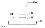
図1Aおよび1Bは、TERAコーティングのようなハード・マスク層のための従来のエッチング・プロセスを示し、その中で本発明を応用できる。図1Aに示されるように、基材101、この基材101上に形成されたTERAコーティングのような薄膜102、およびこの薄膜102上に形成された感光材料層104を有する膜スタック100が形成される。従来のリソグラフィ技術を用いて感光材料層104中にパターン106を形成することができる。図1Bに見られるように、感光層104中のパターン106は、エッチング・ステップを用いて薄膜102に転写される。加えて、例えば、本発明は、図2Aおよび2Bに示される膜スタック110のようなゲート・スタックに応用できる。その中で、基材111、(酸化ケイ素層、または高誘電率酸化物層のような)ゲート酸化物層112、ゲート・ポリシリコン層114、(窒化ケイ素層のような)窒化物層116、酸化物層118、(TERAコーティングのような)ハード・マスク120、(Si、C、O、Hを含有する層のような)キャップ層122、および感光材料層124を有する膜スタック110が形成される。従来のリソグラフィ技術を用いて感光材料層124中にパターン126を形成することができる。図2Bに見られるように、感光層124中のパターン126は、エッチング・ステップを用いてキャップ層122およびハード・マスク120に転写される。
1A and 1B show a conventional etching process for a hard mask layer such as a TERA coating in which the present invention can be applied. As shown in FIG. 1A, a
本発明の一実施形態において、フッ素化プラズマを形成するために、SF6を含有するプロセス・ガスがプラズマ処理システムに導入される。その後、パターンを下にあるTERAコーティングに転写するために、フォトレジストのような感光材料のパターン形成された層を有する基材がプラズマにさらされる。本発明者らは、SF6ベースのエッチング化学的性質を用いてTERAコーティングをエッチングすると、ハード・マスクのエッチング特性が改善されることを見いだした。 In one embodiment of the invention, a process gas containing SF 6 is introduced into the plasma processing system to form a fluorinated plasma. Thereafter, a substrate having a patterned layer of photosensitive material, such as a photoresist, is exposed to plasma to transfer the pattern to the underlying TERA coating. We have found that etching the TERA coating using SF 6 based etch chemistry improves the etch characteristics of the hard mask.
ここで図3を参照すると、別の実施形態において、膜スタック中のTERAコーティングをエッチングする方法が記載される。この方法は、ステップ210において、図1Aおよび1B、または2Aおよび2Bにおけるような基材上にTERAコーティングを形成することから始まるフローチャートとして例示される。TERAコーティングは、化学蒸着法(CVD)、またはプラズマ促進化学蒸着法(PECVD)のような蒸着技術を用いて形成することができる。
Referring now to FIG. 3, in another embodiment, a method for etching a TERA coating in a film stack is described. This method is illustrated in
TERAコーティングは、構造式R:C:H:Xを有し、式中、Rは、Si、Ge、B、Sn、Fe、Ti、およびそれらの組み合わせのうちの少なくとも1つを含む群から選ばれ、Xは、存在しないかまたはO、N、S、およびFのうちの1つ以上を含む群から選ばれる。TERAコーティングは、約1.40<n<2.60の屈折率、および約0.010<k<0.78の吸光係数についての光学範囲を示すように製造できる。また、屈折率および吸光係数のうちの少なくとも1つは、TERAコーティングの厚さ方向に沿って勾配を付ける(または変更する)ことができる。更なる詳細は、米国特許第6,316,167号中に記載されている。さらに、TERAコーティングは、2003年8月21日出願の「調整可能な光学的性質およびエッチング特性を有する材料を蒸着するための方法および装置(Method and apparatus for depositing materials with tunable optical properties and etching characteristics)」と題された係属中の米国特許出願第10/644,958号中でより詳細に記載されるようなPECVDを用いて形成することができ、この米国特許出願は、参照によりその内容全体が本明細書に組み込まれる。屈折率のようなTERAコーティングの光学的性質は、1つまたは複数の下にある層の光学的性質と実質的に一致するように選ばれ得る。例えば、非多孔質誘電性膜のような下にある層は、1.4<n<2.6の範囲の屈折率を達成することを必要とすることがあり、多孔質誘電性膜のような下にある層は、1.2<n<2.6の範囲の屈折率を達成することを必要とすることがある。 The TERA coating has the structural formula R: C: H: X, where R is selected from the group comprising at least one of Si, Ge, B, Sn, Fe, Ti, and combinations thereof. And X is selected from the group that is absent or includes one or more of O, N, S, and F. The TERA coating can be manufactured to exhibit an optical range for a refractive index of about 1.40 <n <2.60 and an extinction coefficient of about 0.010 <k <0.78. Also, at least one of the refractive index and extinction coefficient can be graded (or changed) along the thickness direction of the TERA coating. Further details are described in US Pat. No. 6,316,167. In addition, TERA coatings are filed on August 21, 2003 in “Methods and Apparatus for Depositional Materials with Tunable Optical Properties and Etching”. Can be formed using PECVD as described in more detail in pending US patent application Ser. No. 10 / 644,958, which is hereby incorporated by reference in its entirety. Incorporated herein. The optical properties of the TERA coating, such as the refractive index, can be chosen to substantially match the optical properties of the underlying layer or layers. For example, an underlying layer such as a non-porous dielectric film may need to achieve a refractive index in the range of 1.4 <n <2.6, such as a porous dielectric film. The underlying layer may need to achieve a refractive index in the range of 1.2 <n <2.6.
ステップ220において、感光材料層が基材上に形成される。この感光材料層は、フォトレジストを含み得る。例えば、その感光材料の層(または、複数の層)はトラック・システムを用いて形成することができる。トラック・システムは、248nmレジスト、193nmレジスト、157nmレジスト、EUVレジスト、(トップ/ボトム)反射防止コーティング(TARC/BARC)、およびトップ・コートを処理するために構成できる。例えば、トラック・システムは、東京エレクトロン株式会社(TEL)から市販されているClean Track ACT(R)8、またはClean Track ACT(R)12レジスト塗布・現像システムを含み得る。基材上にフォトレジスト膜を形成するための他のシステムおよび方法は、スピンオン・レジスト技術分野の当業者によく知られている。
In
基材上に感光材料層がひとたび形成されると、この感光材料層は、ステップ230においてマイクロリソグラフィを使用しパターンを用いてパターン形成され、続いて(ポジ型フォトレジストの場合のように)感光材料の照射された領域が、または(ネガ型レジストの場合のように)照射されない領域が、現像溶媒を用いて除去される。マイクロリソグラフィ・システムは、どのような適切な従来のステッピング・リソグラフィ・システム、またはスキャニング・リソグラフィ・システムも含み得る。
Once the photosensitive material layer is formed on the substrate, the photosensitive material layer is patterned with a pattern using microlithography in
ステップ240において、感光材料層中に形成されたパターンは、ドライ・エッチング・プロセスを用いて、下にあるTERAコーティングに転写される。ドライ・エッチング・プロセスは、SF6ベースのエッチング化学的性質を含んでいる。また、エッチング化学的性質は、O2、CO、またはCO2のような酸素含有ガスをさらに含み得る。また、エッチング化学的性質は、N2またはNH3のような窒素含有ガスをさらに含み得る。また、エッチング化学的性質は、希ガス(すなわち、ヘリウム、ネオン、アルゴン、キセノン、クリプトン、ラドン)のような不活性ガスをさらに含み得る。また、エッチング化学的性質は、Cl2、HBr、CHF3、またはCH2F2のような別のハロゲン含有ガスをさらに含み得る。また、エッチング化学的性質は、構造CxFyを有するガス(例えば、CF4、C4F8、C4F6、C3F6、C5F8等)のようなフルオロカーボン・ガスをさらに含み得る。
In
本発明のエッチング・プロセスは、プラズマ処理システム中で実行できる。例えば、図4は、本発明のプロセスを実施するために使用できる代表的なプラズマ処理システム1を示す。この図において見られるように、プラズマ処理システム1は、プラズマ処理チャンバ10、このプラズマ処理チャンバ10に結合された診断システム12、ならびにこの診断システム12およびプラズマ処理チャンバ10に結合されたコントローラ14を含んでいる。コントローラ14は、エッチング・プロセスを含むプロセス・レシピを実行するように構成される。加えて、コントローラ14は、診断システム12から少なくとも1つの終点信号を受け取り、プロセスのための終点を正確に決定するために少なくとも1つの終点信号を後処理するように構成される。例示された実施形態において、図4に描かれたプラズマ処理システム1は、材料処理のためにプラズマを利用する。プラズマ処理システム1は、エッチング・チャンバを含み得る。
The etching process of the present invention can be performed in a plasma processing system. For example, FIG. 4 shows an exemplary
図5に描かれた実施形態によれば、本発明に従って用いられるプラズマ処理システム1aは、プラズマ処理チャンバ10、処理される基材25がその上に取り付けられる基材ホルダ20、および真空ポンプ・システム30を含み得る。基材25は、例えば、半導体基材、ウェーハまたは液晶ディスプレイであり得る。プラズマ処理チャンバ10は、例えば、基材25の表面に隣接する処理領域15におけるプラズマ発生を容易にするように構成できる。イオン化可能なガスまたは混合気体が、(ガス注入パイプまたはガス注入シャワーヘッドのような)ガス注入システムを介して導入され、プロセス圧力は調整される。例えば、制御機構(図示せず)を、真空ポンプ・システム30を絞るために用い得る。プラズマは、所定の材料プロセスに特有の材料を作り出すためおよび/または基材25の露出表面からの材料の除去を支援するために利用できる。プラズマ処理システム1aは、200mm基材、300mm基材、またはそれ以上の基材を処理するように構成できる。
According to the embodiment depicted in FIG. 5, the
基材25は、例えば、静電クランピング・システムを介して基材ホルダ20に取り付けることができる。さらに、基材ホルダ20は、例えば、基材ホルダ20から熱を受け取り、熱交換システム(図示せず)に熱を移し、あるいは加熱の場合には、熱交換システムから熱を移す循環式冷却材フローを含む冷却システムをさらに含み得る。さらに、ガスは、例えば、基材25と基材ホルダ20との間のガスギャップ熱伝導係数を向上するために、背面ガス・システムを介して基材25の背面に送られ得る。そのようなシステムは、基材25の温度制御が高温または低温において必要とされる場合に利用できる。例えば、背面ガス・システムは、2ゾーン・ガス分布システムを含むことができ、ヘリウム・ガス・ギャップ圧力は、基材25の中心とエッジとの間で独立して変え得る。他の実施形態において、抵抗加熱部品、または熱電ヒータ/クーラのような加熱/冷却部品を、プラズマ処理チャンバ10のチャンバ壁およびプラズマ処理システム1a内部のどの他の構成要素だけでなく基材ホルダ20にも組み込むことができる。
The
図5に示される実施形態において、基材ホルダ20は電極を含むことができ、この電極を介してRF電力がプロセス空間15中の処理プラズマに結合される。例えば、基材ホルダ20は、RF発生器40からインピーダンス整合ネットワーク50を通り基材ホルダ20へのRF電力の伝送を介してRF電圧で電気的にバイアスをかけられ得る。RFバイアスは、プラズマを形成し維持するために電子を加熱するのに役立ち得る。この構成において、システムは、反応性イオン・エッチング(RIE)反応器として動作することができ、チャンバおよび上部ガス注入電極は、接地表面として働く。RFバイアスのための典型的な周波数は、0.1MHz〜100MHzの範囲であり得る。プラズマ処理のためのRFシステムは、当業者によく知られている。
In the embodiment shown in FIG. 5, the
また、RF電力は、複数の周波数で基材ホルダ電極に印加される。さらに、インピーダンス適合ネットワーク50は、反射電力を低減することによりプラズマ処理チャンバ10中のプラズマへのRF電力の転送を改善するのに役立つ。整合ネットワーク配列(例えば、Lタイプ、πタイプ、Tタイプ等)および自動制御方法は、当業者によく知られている。
RF power is applied to the substrate holder electrode at a plurality of frequencies. Furthermore, the
真空ポンプ・システム30は、例えば、最高5000リットル/秒(およびそれ以上)の排気速度が可能なターボ分子真空ポンプ(TMP)およびチャンバ圧力を絞るためのゲート・バルブを含み得る。ドライ・プラズマ・エッチング用に利用される従来のプラズマ処理デバイスにおいて、1000〜3000リットル/秒TMPが一般に用いられる。TMPは、一般に50mTorr未満の低圧処理に有用である。高圧処理(すなわち、100mTorr以上)については、メカニカル・ブースター・ポンプおよびドライ粗引きポンプが使用できる。さらに、チャンバ圧力を監視するためのデバイス(図示せず)を、プラズマ処理チャンバ10に結合することができる。圧力測定デバイスは、例えば、MSK Instruments,Inc.(マサチューセッツ州アンドーバー)から市販されているType 628B Baratron(R)絶対キャパシタンス・マノメータであり得る。
The
コントローラ14は、マイクロプロセッサ、メモリ、そしてプラズマ処理システム1aへの入力を通信および起動ならびにプラズマ処理システム1aからの出力を監視するのに十分な制御電圧を発生することが可能なデジタルI/Oポートを含む。さらに、コントローラ14は、RF発生器40、インピーダンス整合ネットワーク50、ガス注入システム(図示せず)、真空ポンプ・システム30、診断システム12、ならびに背面ガス送達システム(図示せず)、基材/基材ホルダ温度測定システム(図示せず)、および/または静電クランピング・システム(図示せず)に結合されかつこれらと情報を交換できる。例えば、メモリ中に格納されたプログラムは、エッチング・プロセスを実行するために、プロセス・レシピに従って、プラズマ処理システム1aの前述の構成要素への入力を起動するために利用できる。コントローラ14の一例は、DELL 社(テキサス州オースチン)から入手可能なDELL PRECISION WORKSTATTION 610(登録商標)である。
The
コントローラ14は、プラズマ処理システム1aに対して局所的に配置されてもよく、または、プラズマ処理システム1aに対して遠隔的に配置されてもよい。例えば、コントローラ14は、直接接続、イントラネット、およびインターネットのうちの少なくとも1つを用いてプラズマ処理システム1aとデータを交換できる。コントローラ14は、例えば、顧客サイト(すなわち、デバイス・メーカー等)においてイントラネットに結合することができ、または、ベンダ・サイト(すなわち、設備製造業者)においてイントラネットに結合できる。加えて、例えば、コントローラ14は、インターネットに結合することができる。さらに、別のコンピュータ(すなわち、コントローラ、サーバ等)が、例えば、直接接続、イントラネット、およびインターネットのうちの少なくとも1つを介してデータを交換するためにコントローラ14にアクセスできる。また、データは、当業者により理解されるように、有線または無線接続を介して転送され得る。
The
診断システム12は、光学式診断サブシステム(図示せず)を含み得る。光学式診断サブシステムは、プラズマから放出された光強度を測定するための(シリコン)フォトダイオードまたは光電子増倍管(PMT)のような検出器を含み得る。診断システム12は、ナローバンド干渉フィルタのような光学フィルタをさらに含み得る。他の実施形態において、診断システム12は、ラインCCD(電荷結合素子)、CID(電荷注入素子)アレイ、および格子またはプリズムのような光分散デバイスのうちの少なくとも1つを含み得る。加えて、診断システム12は、任意の波長で光を測定するためのモノクロメータ(例えば、格子/検出器システム)、または、光スペクトルを測定するための、例えば、米国特許第5,888,337号に記載されるデバイスのような分光計(例えば、回転格子)を含むことができ、この米国特許は、参照によりその全体が本明細書に組み入れられる。
The
診断システム12は、Peak Sensor Systems、またはVerityInstruments,Inc.などからの高解像度発光分光分析(OES:Optical Emission Spectroscopy)センサを含み得る。そのようなOESセンサは、紫外(UV)、可視(VIS)、および近赤外(NIR)光スペクトルにわたる広いスペクトルを有する。解像度は、約1.4オングストロームであり、すなわち、センサは、240〜1000nmの5550波長を集めることができる。例えば、OESセンサは、高感度ミニチュア光ファイバUV−VIS−NIR分光計を装備でき、今度はこの分光計が2048画素リニアCCDアレイと一体化される。
分光計は、単一または束ねた光ファイバを通って伝送される光を受け取り、光ファイバから出力される光は、固定格子を用いてラインCCDアレイ全体にわたって拡散される。上述の構成と同様に、光学式真空窓を通る発光は、凸状球面レンズを介して光ファイバの入力端上に焦点が合わされる。所与のスペクトル範囲(UV、VISおよびNIR)にそれぞれ専用に調整された3つの分光計が、プロセス・チャンバのためのセンサを形成する。各分光計は、独立したA/D変換器を含む。最後に、センサ利用に応じて、全発光スペクトルが0.1〜1.0秒毎に記録できる。 The spectrometer receives light transmitted through a single or bundled optical fiber, and the light output from the optical fiber is diffused across the line CCD array using a fixed grating. Similar to the configuration described above, light emission through the optical vacuum window is focused on the input end of the optical fiber via a convex spherical lens. Three spectrometers, each tuned specifically for a given spectral range (UV, VIS and NIR), form a sensor for the process chamber. Each spectrometer includes an independent A / D converter. Finally, the entire emission spectrum can be recorded every 0.1 to 1.0 seconds depending on the sensor usage.
さらに、診断システム12は、Timbre Technologies,Inc.(2953 Bunker Hill Lane,Suite 301,Santa Clara,CA95054)により提供されるシステムのような、光学式デジタル形状計測を実行するためのシステムを含み得る。
In addition,
図6に示される実施形態において、本発明を実施するために使用できるプラズマ処理システム1bは、例えば、図4または図5の実施形態と同様とすることができ、そして図4および図5に関連して記載された構成要素に加えて、プラズマ密度を場合によっては増大および/またはプラズマ処理均一性を向上するために、固定式か、機械または電気回転式の磁場システム60をさらに含み得る。さらに、コントローラ14は、回転速度および磁場強度を調節するために、磁場システム60に結合することができる。回転磁場のデザインおよび実施は、当業者によく知られている。
In the embodiment shown in FIG. 6, a
図7に示される実施形態において、本発明を実施するために使用できるプラズマ処理システム1cは、例えば、図4または図5の実施形態と同様とすることができ、そしてRF電力がRF発生器72からインピーダンス整合ネットワーク74を通って結合され得る上部電極70をさらに含み得る。上部電極70へRF電力を印加するための典型的な周波数は、0.1MHz〜200MHzの範囲とすることができる。加えて、下部電極へパワーを印加するための典型的な周波数は、0.1MHz〜100MHzの範囲とすることができる。さらに、コントローラ14は、上部電極70へのRF電力の印加を制御するために、RF発生器72およびインピーダンス整合ネットワーク74に結合される。上部電極のデザインおよび実施実行は、当業者によく知られている。
In the embodiment shown in FIG. 7, a
図8に示される実施形態において、本発明を実施するために使用できるプラズマ処理システム1dは、例えば、図4および図5の実施形態と同様とすることができ、そしてRF発生器82を介してインピーダンス整合ネットワーク84を通ってRF電力が結合される誘導コイル80をさらに含み得る。RF電力は、誘導コイル80から誘電窓(図示せず)を通ってプラズマ処理領域15に誘導的に結合される。誘導コイル80へRF電力を印加するための典型的な周波数は、10MHz〜100MHzの範囲とすることができる。同様に、チャック電極へパワーを印加するための典型的な周波数は、0.1MHz〜100MHzの範囲とすることができる。加えて、スロット付きファラデー・シールド(図示せず)を、誘導コイル80とプラズマとの間の容量結合を低減するために用い得る。さらに、コントローラ14は、誘導コイル80へのパワーの印加を制御するために、RF発生器82およびインピーダンス整合ネットワーク84に結合される。他の実施形態において、誘導コイル80は、トランス結合プラズマ(TCP:transformer coupled plasma)反応器におけるように、プラズマ処理領域15と上方から連通する「渦巻き」コイルまたは「パンケーキ」コイルとすることができる。誘導的に結合されたプラズマ(ICP)源、またはトランス結合プラズマ(TCP)源のデザインおよび実施は、当業者によく知られている。
In the embodiment shown in FIG. 8, a
また、プラズマは、電子サイクロトロン共鳴(ECR:electron cyclotron resonance)を用いて形成できる。さらに別の実施形態において、プラズマは、ヘリコン波の発射から形成できる。さらに別の実施形態において、プラズマは、伝搬する表面波から形成できる。上述の各プラズマ源は、当業者によく知られている。 In addition, the plasma can be formed using electron cyclotron resonance (ECR). In yet another embodiment, the plasma can be formed from a helicon wave launch. In yet another embodiment, the plasma can be formed from propagating surface waves. Each plasma source described above is well known to those skilled in the art.
1つの例において、エッチング・プロセスは、図7において説明されたシステムのようなプラズマ処理システムにおいて実行でき、プロセス・パラメータ空間は、約5〜約200mTorrのチャンバ圧力、約5〜約1000sccmの範囲のSF6プロセス・ガス流量、約50〜約500Wの範囲の上部電極(例えば、図7における要素70)RFバイアス、約10〜約500Wの範囲の下部電極(例えば、図7における要素20)RFバイアスを含むことができ、上部電極バイアス周波数は、約0.1MHz〜約200MHzの範囲、例えば、60MHzとすることができ、下部電極バイアス周波数は、約0.1MHz〜約100MHzの範囲、例えば、2MHzとすることができる。
In one example, the etching process can be performed in a plasma processing system, such as the system described in FIG. 7, where the process parameter space ranges from about 5 to about 200 mTorr chamber pressure, about 5 to about 1000 sccm. SF 6 process gas flow rate, upper electrode (eg,
別の例において、表1は、以下の代表的なプロセス・レシピを利用してTERAコーティング中にエッチングされたフィーチャの限界寸法を示す:チャンバ圧力=20mTorr、上部電極RF電力=100W、下部電極RF電力=80W、プロセス・ガス流量SF6=100sccm、電極70(図7参照)の下面と基材ホルダ20上の基材25の上面との間の電極間隔=140mm、下部電極(例えば、図7における基材ホルダ20)温度=30℃、上部電極(例えば、図7における電極70)温度=80℃、チャンバ壁温度=60℃、背面ヘリウム圧力 中心/エッジ=3/3Torr、およびエッチング時間=17秒間。
In another example, Table 1 shows the critical dimensions of features etched during the TERA coating using the following representative process recipe: chamber pressure = 20 mTorr, upper electrode RF power = 100 W, lower electrode RF Electric power = 80 W, process gas flow rate SF 6 = 100 sccm, electrode spacing between the lower surface of the electrode 70 (see FIG. 7) and the upper surface of the

表1のデータは、孤立状フィーチャ(すなわち、フィーチャの広い間隔)およびネスト状フィーチャ(すなわち、フィーチャの密接した間隔)双方について報告される。データは、限界寸法(CD)の維持におけるプロセスの成功を実証している。 The data in Table 1 is reported for both isolated features (ie, wide feature spacing) and nested features (ie, close feature spacing). The data demonstrates the success of the process in maintaining critical dimension (CD).
本発明の特定の代表的実施形態のみが上記で詳細に説明されたが、本発明の新規な教示および利点を著しく逸脱することなく、代表的な実施形態において多くの変更が可能であることを当業者は直ちに認識するであろう。従って、すべてのそのような変更は、本発明の範囲に含まれることが意図される。 While only specific exemplary embodiments of the present invention have been described in detail above, it should be understood that many changes can be made in the exemplary embodiments without significantly departing from the novel teachings and advantages of the present invention. Those skilled in the art will immediately recognize. Accordingly, all such modifications are intended to be included within the scope of this invention.
Claims (30)
前記基材上に調整可能耐エッチング性反射防止(TERA:tunable etch resistant anti−reflective)コーティングを形成するステップであって、前記TERAコーティングは、式R:C:H:Xにより定義される構造を有し、式中、Rは、Si、Ge、B、Sn、Fe、Ti、およびそれらの組み合わせのうちの少なくとも1つを含む群から選ばれ、Xは、存在しないかまたはO、N、S、およびFのうちの1つ以上を含む群から選ばれる、ステップと、
前記TERAコーティング上に感光材料層を形成するステップと、
前記感光材料層中にパターンを形成するステップと、
少なくともSF6を含むエッチング・プロセスを用いて、前記パターンを前記TERAコーティングに転写するステップとを含む、
方法。 A method of providing a structure on a substrate,
Forming a tunable etch resistant anti-reflective (TERA) coating on the substrate, wherein the TERA coating has a structure defined by the formula R: C: H: X Wherein R is selected from the group comprising at least one of Si, Ge, B, Sn, Fe, Ti, and combinations thereof, and X is absent or O, N, S And a step selected from the group comprising one or more of F;
Forming a photosensitive material layer on the TERA coating;
Forming a pattern in the photosensitive material layer;
Using an etching process including at least SF 6, and a step of transferring the pattern to the TERA coating,
Method.
基材をプラズマ処理システム中に配置するステップであって、前記基材は、前記TERAコーティングを有し、該TERAコーティングは、式R:C:H:Xにより定義される構造を有し、式中、Rは、Si、Ge、B、Sn、Fe、Ti、およびそれらの組み合わせのうちの少なくとも1つを含む群から選ばれ、Xは、存在しないかまたはO、N、S、およびFのうちの1つ以上を含む群から選ばれる、ステップと、
少なくともSF6を含むプロセス・ガスを導入するステップと、
前記プロセス・ガスからプラズマを形成するステップと、
前記基材を前記プラズマにさらすステップとを含む、
方法。 A method of etching a TERA coating comprising:
Placing a substrate in a plasma processing system, wherein the substrate has the TERA coating, the TERA coating having a structure defined by the formula R: C: H: X, Wherein R is selected from the group comprising at least one of Si, Ge, B, Sn, Fe, Ti, and combinations thereof, and X is absent or of O, N, S, and F A step selected from the group comprising one or more of them;
Introducing a process gas comprising at least SF 6 ;
Forming a plasma from the process gas;
Exposing the substrate to the plasma.
Method.
プロセス・チャンバと、
該プロセス・チャンバ内に配置され、かつ前記基材を支持するように構成された基材ホルダであって、前記基材は、式R:C:H:Xにより定義される構造を有するTERAコーティングを含み、式中、Rは、Si、Ge、B、Sn、Fe、Ti、およびそれらの組み合わせのうちの少なくとも1つを含む群から選ばれ、Xは、存在しないかまたはO、N、S、およびFのうちの1つ以上を含む群から選ばれる、基材ホルダと、
前記プロセス・チャンバに結合され、かつ少なくともSF6を含むプロセス・ガスを導入するように構成されたガス注入システムと、
前記プロセス・チャンバに結合され、かつ前記プロセス・ガスからプラズマを形成するように構成されたプラズマ源とを含む、
システム。 A plasma processing system for etching a TERA coating on a substrate, comprising:
A process chamber;
A substrate holder disposed in the process chamber and configured to support the substrate, the substrate having a structure defined by the formula R: C: H: X Wherein R is selected from the group comprising at least one of Si, Ge, B, Sn, Fe, Ti, and combinations thereof, and X is absent or O, N, S A substrate holder selected from the group comprising one or more of F and
A gas injection system coupled to the process chamber and configured to introduce a process gas comprising at least SF 6 ;
A plasma source coupled to the process chamber and configured to form a plasma from the process gas;
system.
請求項21に記載のシステム。 A controller coupled to the gas injection system and configured to control a flow rate of the process gas;
The system of claim 21.
Applications Claiming Priority (2)
| Application Number | Priority Date | Filing Date | Title |
|---|---|---|---|
| US10/926,404 US20060049139A1 (en) | 2004-08-26 | 2004-08-26 | Method and system for etching a gate stack |
| PCT/US2005/023943 WO2006025944A1 (en) | 2004-08-26 | 2005-06-30 | Method and system for etching a gate stack |
Publications (2)
| Publication Number | Publication Date |
|---|---|
| JP2008511167A true JP2008511167A (en) | 2008-04-10 |
| JP2008511167A5 JP2008511167A5 (en) | 2008-07-31 |
Family
ID=35058277
Family Applications (1)
| Application Number | Title | Priority Date | Filing Date |
|---|---|---|---|
| JP2007529849A Withdrawn JP2008511167A (en) | 2004-08-26 | 2005-06-30 | Method and system for etching a gate stack |
Country Status (5)
| Country | Link |
|---|---|
| US (1) | US20060049139A1 (en) |
| JP (1) | JP2008511167A (en) |
| KR (1) | KR20070051846A (en) |
| TW (1) | TWI286840B (en) |
| WO (1) | WO2006025944A1 (en) |
Families Citing this family (6)
| Publication number | Priority date | Publication date | Assignee | Title |
|---|---|---|---|---|
| US8158526B2 (en) * | 2006-10-30 | 2012-04-17 | Applied Materials, Inc. | Endpoint detection for photomask etching |
| US8741394B2 (en) | 2010-03-25 | 2014-06-03 | Novellus Systems, Inc. | In-situ deposition of film stacks |
| US9028924B2 (en) * | 2010-03-25 | 2015-05-12 | Novellus Systems, Inc. | In-situ deposition of film stacks |
| US9165788B2 (en) | 2012-04-06 | 2015-10-20 | Novellus Systems, Inc. | Post-deposition soft annealing |
| US9117668B2 (en) | 2012-05-23 | 2015-08-25 | Novellus Systems, Inc. | PECVD deposition of smooth silicon films |
| US9388491B2 (en) | 2012-07-23 | 2016-07-12 | Novellus Systems, Inc. | Method for deposition of conformal films with catalysis assisted low temperature CVD |
Family Cites Families (22)
| Publication number | Priority date | Publication date | Assignee | Title |
|---|---|---|---|---|
| US3729728A (en) * | 1971-05-10 | 1973-04-24 | Spearhead Inc | Capacitive switching device |
| US3986372A (en) * | 1976-01-16 | 1976-10-19 | Whirlpool Corporation | Appliance programmer including a safety circuit |
| US4748296A (en) * | 1986-12-03 | 1988-05-31 | General Electric Company | Push-to-start control switch |
| US5161393A (en) * | 1991-06-28 | 1992-11-10 | General Electric Company | Electronic washer control including automatic load size determination, fabric blend determination and adjustable washer means |
| IT226476Z2 (en) * | 1992-04-14 | 1997-06-24 | Whirlpool Italia | DEVICE SUITABLE FOR CHECKING AND COMMANDING THE OPERATION OF A WASHING MACHINE OR SIMILAR OR OTHER HOME APPLIANCES SUCH AS OVEN HOB OR SIMILAR WITH A SERVO-ASSISTED KNOB |
| US5301523A (en) * | 1992-08-27 | 1994-04-12 | General Electric Company | Electronic washer control including automatic balance, spin and brake operations |
| US5464955A (en) * | 1993-04-15 | 1995-11-07 | Emerson Electric Co. | Backlit appliance control console |
| JP3193265B2 (en) * | 1995-05-20 | 2001-07-30 | 東京エレクトロン株式会社 | Plasma etching equipment |
| US5668359A (en) * | 1996-03-01 | 1997-09-16 | Eaton Corporation | Multiple switch assembly including spring biased rotary cam with concentric cam tracks for selectively operating switches |
| US6316167B1 (en) * | 2000-01-10 | 2001-11-13 | International Business Machines Corporation | Tunabale vapor deposited materials as antireflective coatings, hardmasks and as combined antireflective coating/hardmasks and methods of fabrication thereof and application thereof |
| DE19928229A1 (en) * | 1999-06-19 | 2000-12-21 | Mannesmann Vdo Ag | Retractable knob |
| JP3968020B2 (en) * | 2001-02-24 | 2007-08-29 | マルクアルト ゲーエムベーハー | Rotation angle adjustment device |
| US7196604B2 (en) * | 2001-05-30 | 2007-03-27 | Tt Electronics Technology Limited | Sensing apparatus and method |
| US6727443B2 (en) * | 2001-08-06 | 2004-04-27 | Emerson Electric Co. | Appliance control system with knob control assembly |
| US6813524B2 (en) * | 2001-08-06 | 2004-11-02 | Emerson Electric Co. | Appliance control system with auxiliary inputs |
| US6862482B2 (en) * | 2001-08-06 | 2005-03-01 | Emerson Electric Co. | Appliance control system with LED operation indicators |
| JP2003124189A (en) * | 2001-10-10 | 2003-04-25 | Fujitsu Ltd | Method of manufacturing semiconductor device |
| DE10203509B4 (en) * | 2002-01-30 | 2005-01-13 | Whirlpool Corp., Benton Harbor | Locking device for a multi-level rotary switch |
| KR100915231B1 (en) * | 2002-05-17 | 2009-09-02 | 삼성전자주식회사 | Deposition method of insulating layers having low dielectric constant of semiconductor device, a thin film transistor substrate using the same and a method of manufacturing the same |
| US6630395B1 (en) * | 2002-10-24 | 2003-10-07 | International Business Machines Corporation | Methods for fabricating electrical connections to semiconductor structures incorporating low-k dielectric materials |
| US6869542B2 (en) * | 2003-03-12 | 2005-03-22 | International Business Machines Corporation | Hard mask integrated etch process for patterning of silicon oxide and other dielectric materials |
| US7199046B2 (en) * | 2003-11-14 | 2007-04-03 | Tokyo Electron Ltd. | Structure comprising tunable anti-reflective coating and method of forming thereof |
-
2004
- 2004-08-26 US US10/926,404 patent/US20060049139A1/en not_active Abandoned
-
2005
- 2005-06-30 KR KR1020077002485A patent/KR20070051846A/en not_active Application Discontinuation
- 2005-06-30 WO PCT/US2005/023943 patent/WO2006025944A1/en active Application Filing
- 2005-06-30 JP JP2007529849A patent/JP2008511167A/en not_active Withdrawn
- 2005-08-10 TW TW094127126A patent/TWI286840B/en not_active IP Right Cessation
Also Published As
| Publication number | Publication date |
|---|---|
| KR20070051846A (en) | 2007-05-18 |
| US20060049139A1 (en) | 2006-03-09 |
| TWI286840B (en) | 2007-09-11 |
| TW200612554A (en) | 2006-04-16 |
| WO2006025944A1 (en) | 2006-03-09 |
Similar Documents
| Publication | Publication Date | Title |
|---|---|---|
| JP4861987B2 (en) | Method and system for etching a film stack | |
| US7846645B2 (en) | Method and system for reducing line edge roughness during pattern etching | |
| WO2005091796A2 (en) | Method and system for treating a hard mask to improve etch characteristics | |
| US20050221619A1 (en) | System and method for etching a mask | |
| US7531461B2 (en) | Process and system for etching doped silicon using SF6-based chemistry | |
| JP5106424B2 (en) | Method and system for selective etching of dielectric material to silicon | |
| US7465673B2 (en) | Method and apparatus for bilayer photoresist dry development | |
| JP2008511167A (en) | Method and system for etching a gate stack | |
| JP2006522480A (en) | Method and apparatus for dry development of multilayer photoresist | |
| US7344991B2 (en) | Method and apparatus for multilayer photoresist dry development | |
| US20050136681A1 (en) | Method and apparatus for removing photoresist from a substrate | |
| US8048325B2 (en) | Method and apparatus for multilayer photoresist dry development | |
| US20070056927A1 (en) | Process and system for etching doped silicon | |
| US7767926B2 (en) | Method and system for dry development of a multi-layer mask using sidewall passivation and mask passivation | |
| US20050136666A1 (en) | Method and apparatus for etching an organic layer |
Legal Events
| Date | Code | Title | Description |
|---|---|---|---|
| RD02 | Notification of acceptance of power of attorney |
Free format text: JAPANESE INTERMEDIATE CODE: A7422 Effective date: 20080508 |
|
| A621 | Written request for application examination |
Free format text: JAPANESE INTERMEDIATE CODE: A621 Effective date: 20080513 |
|
| A521 | Written amendment |
Free format text: JAPANESE INTERMEDIATE CODE: A523 Effective date: 20080529 |
|
| A761 | Written withdrawal of application |
Free format text: JAPANESE INTERMEDIATE CODE: A761 Effective date: 20090406 |