JP2008190884A - Acceleration detector - Google Patents
Acceleration detector Download PDFInfo
- Publication number
- JP2008190884A JP2008190884A JP2007022658A JP2007022658A JP2008190884A JP 2008190884 A JP2008190884 A JP 2008190884A JP 2007022658 A JP2007022658 A JP 2007022658A JP 2007022658 A JP2007022658 A JP 2007022658A JP 2008190884 A JP2008190884 A JP 2008190884A
- Authority
- JP
- Japan
- Prior art keywords
- fork type
- circuit
- tuning
- acceleration
- acceleration detection
- Prior art date
- Legal status (The legal status is an assumption and is not a legal conclusion. Google has not performed a legal analysis and makes no representation as to the accuracy of the status listed.)
- Withdrawn
Links
- 230000001133 acceleration Effects 0.000 title claims abstract description 79
- 238000001514 detection method Methods 0.000 claims abstract description 46
- 230000004069 differentiation Effects 0.000 claims abstract description 11
- 230000010355 oscillation Effects 0.000 claims description 28
- 230000008878 coupling Effects 0.000 claims description 16
- 238000010168 coupling process Methods 0.000 claims description 16
- 238000005859 coupling reaction Methods 0.000 claims description 16
- 239000013078 crystal Substances 0.000 abstract description 54
- 230000035945 sensitivity Effects 0.000 abstract description 11
- 239000000284 extract Substances 0.000 abstract description 2
- 230000035882 stress Effects 0.000 description 26
- 230000008859 change Effects 0.000 description 7
- 239000003990 capacitor Substances 0.000 description 5
- 238000010586 diagram Methods 0.000 description 4
- 239000000758 substrate Substances 0.000 description 4
- 230000032683 aging Effects 0.000 description 2
- 238000005452 bending Methods 0.000 description 2
- 238000000034 method Methods 0.000 description 2
- 230000008569 process Effects 0.000 description 2
- 239000010453 quartz Substances 0.000 description 2
- 239000004065 semiconductor Substances 0.000 description 2
- VYPSYNLAJGMNEJ-UHFFFAOYSA-N silicon dioxide Inorganic materials O=[Si]=O VYPSYNLAJGMNEJ-UHFFFAOYSA-N 0.000 description 2
- 230000008901 benefit Effects 0.000 description 1
- 230000001934 delay Effects 0.000 description 1
- 238000006073 displacement reaction Methods 0.000 description 1
- 239000007789 gas Substances 0.000 description 1
- HFGPZNIAWCZYJU-UHFFFAOYSA-N lead zirconate titanate Chemical compound [O-2].[O-2].[O-2].[O-2].[O-2].[Ti+4].[Zr+4].[Pb+2] HFGPZNIAWCZYJU-UHFFFAOYSA-N 0.000 description 1
- 239000007788 liquid Substances 0.000 description 1
- 230000007246 mechanism Effects 0.000 description 1
Images


Landscapes
- Gyroscopes (AREA)
- Oscillators With Electromechanical Resonators (AREA)
- Piezo-Electric Or Mechanical Vibrators, Or Delay Or Filter Circuits (AREA)
Abstract
【課題】温度感度安定度に優れた加速度検出装置を提供する。
【解決手段】第1の音叉型水晶振動素子20aを共振子として備えたOSC2と、第2の音叉型水晶振動素子20bを共振子として備えたVCXO4と、VCXO4から出力される出力信号の位相とOSC2から出力される基準信号の位相を比較する位相比較回路3と、位相比較回路3から出力される位相差信号の低域成分を抽出するLPF4と、LPF4から出力される出力信号を微分する微分回路6と、時定数回路を備えLPF4の出力信号に応じた制御電圧をVCXO4にフィードバックするDCサーボ回路8とを備え、第1及び第2の音叉型水晶振動素子20a、20bは、加速度検出軸方向を一致させ、且つ、第1及び第2の音叉型水晶振動素子20a、20bにおいて検出する加速度検出方向が逆向きとなるように配置し、微分回路6から出力される出力信号を加速度検出信号として出力する。
【選択図】図1An acceleration detection device having excellent temperature sensitivity stability is provided.
An OSC2 including a first tuning-fork type crystal resonator element 20a as a resonator, a VCXO4 including a second tuning-fork type crystal resonator element 20b as a resonator, and a phase of an output signal output from the VCXO4 Phase comparison circuit 3 that compares the phase of the reference signal output from the OSC 2, LPF 4 that extracts a low frequency component of the phase difference signal output from the phase comparison circuit 3, and differentiation that differentiates the output signal output from the LPF 4 A circuit 6 and a DC servo circuit 8 that includes a time constant circuit and feeds back a control voltage according to the output signal of the LPF 4 to the VCXO 4, and the first and second tuning-fork type crystal vibrating elements 20 a and 20 b have acceleration detection axes The direction is matched and the first and second tuning-fork type crystal vibrating elements 20a and 20b are arranged so that the acceleration detection directions are opposite to each other. Outputting an output signal outputted from the road 6 as an acceleration detection signal.
[Selection] Figure 1
Description
本発明は圧電振動素子を用いて加速度を検出する加速度検出装置に関するものである。 The present invention relates to an acceleration detection device that detects acceleration using a piezoelectric vibration element.
近年、加速度を検出する加速度センサは、次世代の自動車、ロボット、宇宙産業など幅広い応用を目指して研究、開発が行われている。民生機器向けに開発されている加速度センサは、加速度検知機構を半導体プロセスにより作製したMEMS(Micro Electro Mechanical Systems)センサが良く知られている。
一方、例えば気体や液体などの圧力の測定を行う圧力センサ等においてはMEMSセンサ以外にも音叉型振動子を利用したものが開発されている。
In recent years, acceleration sensors that detect acceleration have been researched and developed for a wide range of applications such as next-generation automobiles, robots, and the space industry. As an acceleration sensor developed for consumer equipment, a MEMS (Micro Electro Mechanical Systems) sensor in which an acceleration detection mechanism is manufactured by a semiconductor process is well known.
On the other hand, for example, pressure sensors for measuring pressures of gases and liquids have been developed using tuning fork vibrators in addition to MEMS sensors.
図6は、特許文献1に開示されている従来の振動式センサ回路の構成を示した図である。図6に示す従来のセンサ回路100は、センサ部101とドライブ回路102により構成される。センサ部101はセンサ素子である振動子101a、アンプ101b、整流回路101cを有して構成される。振動子101aは、例えばチタン酸ジルコン酸鉛(PZT:lead zirconium titanate)が組付けられた振動子である。ドライブ回路102は、電圧制御発振器102a、アンプ102b、位相比較器102cを有して構成される。
このように構成されるセンサ回路100では、センサ部101の振動子101aがドライブ回路部102の電圧制御発振器102aにより駆動される。
FIG. 6 is a diagram showing a configuration of a conventional vibration sensor circuit disclosed in Patent Document 1. In FIG. A
In the
ここで、振動子101aが物理的な応力(圧力)を受けると、振動子101aの共振周波数が変化する。振動子101aの共振周波数が変化すると、ドライブ回路102の位相比較器102cから出力される出力信号の位相が変動する。これにより、電圧制御発振器102aの出力信号は振動子101aの共振周波数と一致するように制御され、振動子101aは応力に応じた共振周波数で振動することになる。よって、ライン104または103の出力を検知信号として取り出すことで振動子101aが受けた応力値を検知することができる。
ところで、上記したような半導体プロセスにより作製したMEMSセンサ、或いは図6に示した振動式センサ回路100は、周波数−温度特性が悪いため、周囲温度によって加速度感度に誤差が生じるという欠点があった。
またMEMSセンサは、規定以上の強い加速度が加わった場合、センサが破壊されてしまうという欠点がった。
本発明は上記したような点を鑑みてなされたものであり、温度感度安定度に優れた加速度検出装置を提供することを目的とする。また強い加速度が加わった場合でも破壊されることがない加速度検出装置を提供することを目的とする。
Incidentally, the MEMS sensor manufactured by the semiconductor process as described above or the vibration
In addition, the MEMS sensor has a drawback in that the sensor is destroyed when a strong acceleration exceeding a specified value is applied.
The present invention has been made in view of the above-described points, and an object of the present invention is to provide an acceleration detection device having excellent temperature sensitivity stability. It is another object of the present invention to provide an acceleration detection device that is not destroyed even when strong acceleration is applied.
上記目的を達成するため、第1の応力感応素子を共振子として備えた発振回路と、第2の応力感応素子を共振子として備えた電圧制御型圧電発振回路と、発振回路から出力される出力信号と電圧制御型圧電発振回路から出力される出力信号の位相を比較する位相比較回路と、位相比較回路から出力される位相差信号の低域成分を抽出するローパスフィルタと、ローパスフィルタから出力される出力信号を微分する微分回路とローパスフィルタの出力信号に応じた制御電圧を電圧制御型圧電発振回路にフィードバックする直流サーボ回路と、を備え、第1及び第2の応力感応素子は、加速度を検出する加速度検出軸方向を一致させ、且つ、第1及び第2の応力感応素子において検出する加速度検出方向が逆向きとなるように配置して、微分回路の出力信号を加速度検出信号として出力するようにした。
このような本発明によれば、発振回路の出力信号と電圧制御型圧電発振回路の出力信号との位相を位相比較回路で比較し、その位相比較結果をローパスフィルタにより直流化し、さらに微分回路で微分することにより、発振回路に備えた第1の応力感応素子と、電圧制御型圧電発振回路に備えた第2の応力感応素子とを利用して加速度を検出ことが可能になる。
また従来のように電圧制御型発振回路を設けることなく構成することができるので、従来の振動式センサ回路のように加速度以外の強い衝撃が加わった場合でも発振が停止するといったことがない。
To achieve the above object, an oscillation circuit including a first stress sensitive element as a resonator, a voltage control type piezoelectric oscillation circuit including a second stress sensitive element as a resonator, and an output output from the oscillation circuit Output from the phase comparison circuit that compares the phase of the signal and the output signal output from the voltage-controlled piezoelectric oscillation circuit, the low-pass filter that extracts the low-frequency component of the phase difference signal output from the phase comparison circuit, and the low-pass filter And a DC servo circuit that feeds back a control voltage corresponding to the output signal of the low-pass filter to the voltage-controlled piezoelectric oscillation circuit. The first and second stress-sensitive elements have accelerations. A differential circuit in which the acceleration detection axis directions to be detected are made coincident and the acceleration detection directions to be detected in the first and second stress sensitive elements are opposite to each other. An output signal to output as an acceleration detection signal.
According to the present invention, the phase of the output signal of the oscillation circuit and the output signal of the voltage control type piezoelectric oscillation circuit are compared by the phase comparison circuit, the phase comparison result is converted into a direct current by the low-pass filter, and further, the differentiation circuit is used. By differentiating, acceleration can be detected using the first stress sensitive element provided in the oscillation circuit and the second stress sensitive element provided in the voltage control type piezoelectric oscillation circuit.
Further, since it can be configured without providing a voltage-controlled oscillation circuit as in the prior art, oscillation does not stop even when a strong impact other than acceleration is applied unlike the conventional vibration sensor circuit.
本発明の加速度検出装置は、第1及び第2の応力感応素子が第1及び第2の音叉型振動素子により構成され、第1及び第2の音叉型振動素子は、それぞれ並列に配置された2本の振動腕と、該2本の振動腕の延長方向一端を結合する結合部とを有し、第1及び第2の音叉型振動素子の各振動腕の延長方向を加速度検出軸方向と一致させることを特徴とする。このような本発明によれば、加速度を検知する第1及び第2の応力感応素子として音叉型振動素子を利用することが可能になる。 In the acceleration detecting device of the present invention, the first and second stress sensitive elements are constituted by the first and second tuning fork type vibration elements, and the first and second tuning fork type vibration elements are respectively arranged in parallel. Two vibrating arms and a coupling portion for coupling one ends of the extending directions of the two vibrating arms, and the extending directions of the vibrating arms of the first and second tuning-fork type vibrating elements are defined as acceleration detection axis directions It is characterized by matching. According to the present invention, the tuning fork type vibration element can be used as the first and second stress sensitive elements for detecting acceleration.
本発明の加速度検出装置は、第1及び第2の応力感応素子は、第1及び第2の双音叉型振動素子により構成され、第1及び第2の双音叉型振動素子は、それぞれ並列に配置された2本の振動腕と、該2本の振動腕の延長方向の両端を夫々結合した結合部と、を有する双音叉型振動素子であり、結合部の何れか一方を固定端、他方を自由端とし、2本の振動腕の延長方向を加速検出方向と一致させるよう配置したことを特徴とする。このような本発明によれば、加速度を検知する第1及び第2の応力感応素子として、双音叉型振動素子を用いることが可能になるので、音叉型振動素子を用いた場合より応力感度を高めることができる。 In the acceleration detecting device of the present invention, the first and second stress sensitive elements are constituted by first and second double tuning fork type vibration elements, and the first and second double tuning fork type vibration elements are respectively connected in parallel. It is a double tuning fork type vibration element having two arranged vibrating arms and a coupling part that couples both ends in the extending direction of the two vibrating arms, and either one of the coupling parts is a fixed end, and the other , And the extension direction of the two vibrating arms is arranged so as to coincide with the acceleration detection direction. According to the present invention as described above, since it is possible to use a double tuning fork type vibration element as the first and second stress sensitive elements for detecting acceleration, stress sensitivity can be improved as compared with the case where a tuning fork type vibration element is used. Can be increased.
以下、図面を参照して本発明の実施形態について説明する。
図1は、本発明の実施形態に係る加速度検出装置の構成を示したブロック図である。
この図1に示す加速度検出装置1は、発振回路(以下、OSC(Oscillator)と称する)2、位相比較回路3、電圧制御型水晶発振回路(以下、VCXO(Voltage Controlled crystal Oscillator)と称する)4、ローパスフィルタ(以下、LPFと称する)5、微分回路6、緩衝増幅回路(以下、バッファアンプと称する)7、及びDCサーボ回路8により構成される。
OSC2は、例えば第1の応力感応素子として第1の音叉型水晶振動素子20aを備え、所定の周波数で発振する。
位相比較回路3は、OSC2から出力される出力信号の位相とVCXO4から出力される出力信号の位相を比較し、その比較結果を出力する。
Hereinafter, embodiments of the present invention will be described with reference to the drawings.
FIG. 1 is a block diagram showing a configuration of an acceleration detection device according to an embodiment of the present invention.
1 includes an oscillation circuit (hereinafter referred to as OSC (Oscillator)) 2, a phase comparison circuit 3, and a voltage controlled crystal oscillation circuit (hereinafter referred to as VCXO (Voltage Controlled Crystal Oscillator)) 4. , A low-pass filter (hereinafter referred to as LPF) 5, a differentiation circuit 6, a buffer amplifier circuit (hereinafter referred to as buffer amplifier) 7, and a DC servo circuit 8.
The OSC 2 includes, for example, a first tuning-fork type
The phase comparison circuit 3 compares the phase of the output signal output from the OSC 2 with the phase of the output signal output from the VCXO 4 and outputs the comparison result.
VCXO4は、第2の応力感応素子として上記第1の音叉型水晶振動素子20aと同一特性を有する第2の音叉型水晶振動素子20bを備える。第2の音叉型水晶振動素子20bは、VCXO4の共振子として機能すると共に、加速度を検出する加速度検出素子としても機能する。またVCXO4では、DCサーボ回路8の出力信号を制御電圧VcontとしてVCXO4の可変容量ダイオードに印加することにより発振ループの負荷容量を変化させて出力信号の発振周波数が一定となるよう制御している。但し、後述するようにDCサーボ回路8は時定数回路を備え、VCXO4の周波数追従速度が遅くなるように構成されている。
LPF5は、位相比較回路3から出力される位相差信号を直流化して出力する。LPF5の出力信号は、微分回路6に出力されると共に、その一部がDCサーボ回路8にも入力される。
The VCXO 4 includes a second tuning-fork type
The LPF 5 converts the phase difference signal output from the phase comparison circuit 3 into a direct current and outputs it. The output signal of the LPF 5 is output to the differentiation circuit 6 and a part thereof is also input to the DC servo circuit 8.
微分回路6はLPF5からの位相差信号を微分して出力する。
ここで、微分回路6の機能について説明する。
例えば、本実施形態のように音叉型水晶振動素子等を加速度センサとして加速度検出を行う場合は、加速度値とセンサ周波数の周波数変位とが比例関係になる。即ち、加速度∝Δセンサ周波数(FM検波出力)の関係を満たすことになる。
しかし、本実施形態では、位相比較回路3において、OSC2から得られる周波数と、VCXO4から得られる周波数の位相比較をしているので、位相比較回路3からは位相検波出力Φが得られることになる。この位相検波出力Φは、Δセンサ周波数を積分値と等しくなる。即ち、位相検波出力Φ=∫センサ周波数(FM検波出力)の関係を満たすことになる。そこで、本実施形態の加速度検出装置では、LPF5の後段に微分回路6を設け、微分回路6において、LPF5から出力される位相検波出力Φを微分することにより加速度値を得るようにしている。即ち、FM検波=dΦ/dt∝加速度の関係を満たすようにしている。
The differentiation circuit 6 differentiates and outputs the phase difference signal from the LPF 5.
Here, the function of the differentiating circuit 6 will be described.
For example, when performing acceleration detection using a tuning fork type crystal vibrating element or the like as an acceleration sensor as in the present embodiment, the acceleration value and the frequency displacement of the sensor frequency are in a proportional relationship. That is, the relationship of acceleration ∝Δ sensor frequency (FM detection output) is satisfied.
However, in this embodiment, since the phase comparison circuit 3 compares the frequency obtained from the OSC 2 and the frequency obtained from the VCXO 4, the phase detection output Φ is obtained from the phase comparison circuit 3. . This phase detection output Φ is equal to the integral value of the Δ sensor frequency. That is, the relationship of phase detection output Φ = ∫ sensor frequency (FM detection output) is satisfied. Therefore, in the acceleration detection device of the present embodiment, the differentiation circuit 6 is provided after the LPF 5, and the differentiation value is obtained by differentiating the phase detection output Φ output from the LPF 5 in the differentiation circuit 6. That is, the relationship of FM detection = dΦ / dt∝acceleration is satisfied.
DCサーボ回路8は、例えば抵抗R、コンデンサCからなる時定数回路と、オペアンプOP等により構成され、LPF5からの出力信号を遅延させて制御電圧VcontとしてVCXO4にフィードバックするようにしている。
このように構成される本実施形態の加速度検出装置1においては、OSC2の出力信号とVCXO4の出力信号との位相を位相比較回路3で比較し、その位相比較結果をLPF5により直流化し、さらに微分回路6で微分することにより、OSC2に備えた第1の音叉型水晶振動素子20aと、VCXO4に備えた第2の音叉型水晶振動素子20bとを利用して加速度を検出することが可能になる。
The DC servo circuit 8 is constituted by a time constant circuit including, for example, a resistor R and a capacitor C, an operational amplifier OP, and the like, and delays an output signal from the LPF 5 and feeds it back to the VCXO 4 as a control voltage Vcont.
In the acceleration detection device 1 of the present embodiment configured as described above, the phase comparison circuit 3 compares the phases of the output signal of the OSC 2 and the output signal of the VCXO 4, and the phase comparison result is converted into a direct current by the LPF 5 and further differentiated Differentiation by the circuit 6 makes it possible to detect acceleration using the first tuning-fork type
さらに本実施形態の加速度検出装置1では、LPF5の出力に応じた制御電圧を、DCサーボ回路8を介してVCXO4にフィードバックしている。このようなDCサーボ回路8によるフィードバック制御がない場合、例えばOSC2の発振周波数やVCXO4の共振周波数が温度ドリフトにより変化した場合、加速度が「0」であるにも関わらず位相差が発生してしまう。因みに、第1及び第2の音叉型水晶振動素子20a、20bの周波数が同じように温度ドリフトした場合でもOSC2及びVCXO4の回路構成の違いや、第1及び第2の音叉型水晶振動素子20a、20bの経時変化(エージング)の違いなどにより位相差が発生する。そこで、本実施形態では、LPF5の出力に応じた制御電圧を、DCサーボ回路8を介してVCXO4にフィードバックすることで、例えばVCXO4やOSC2の共振周波数の温度ドリフトを補正するようにした。これにより、OSC2に温度補償回路など付加することなく低コストで、温度ドリフト等の影響がない高精度の加速度検出が可能になる。
Further, in the acceleration detection device 1 of the present embodiment, a control voltage corresponding to the output of the LPF 5 is fed back to the VCXO 4 via the DC servo circuit 8. When there is no feedback control by the DC servo circuit 8 as described above, for example, when the oscillation frequency of the OSC 2 or the resonance frequency of the VCXO 4 changes due to temperature drift, a phase difference occurs even though the acceleration is “0”. . Incidentally, even when the frequency of the first and second tuning-fork type
図2は上記したVCXO4の回路構成の一例を示した図である。
この図2に示すVCXO4は、発振回路として位相反転増幅器(以下、MOSインバータと称する)IC1を備える。MOSインバータIC1の入出力間には自己バイアス用の帰還抵抗R1及びコンデンサC1と音叉型水晶振動素子20bとを直列に接続した直列回路が夫々並列に接続されている。さらにMOSインバータIC1の出力端と音叉型水晶振動素子20bとの接続点とグランド(GND)間にはコンデンサC2が接続され、コンデンサC1と音叉型水晶振動素子20bとの接続点とグランド(GND)間に可変容量ダイオードD1が接続されている。可変容量ダイオードD1は、そのアノードが接地側に、カソードが音叉型水晶振動素子20bにそれぞれ接続されている。
FIG. 2 is a diagram showing an example of the circuit configuration of the VCXO 4 described above.
The VCXO 4 shown in FIG. 2 includes a phase inverting amplifier (hereinafter referred to as a MOS inverter) IC1 as an oscillation circuit. Between the input and output of the MOS inverter IC1, a series circuit in which a feedback resistor R1 and a capacitor C1 for self-bias and a tuning fork type
このように構成されるVCXO4においては、音叉型水晶振動素子20b、コンデンサC1、C2、可変容量ダイオードD1により発振ループが構成されることになる。従って、この発振ループを構成する可変容量ダイオードD1のカソードに抵抗R2を介して制御電圧Vcontを印加して可変容量ダイオードD1の容量を可変することで、発振ループの負荷容量を変化させて発振周波数が所定の発振周波数となるよう制御可能に構成されている。また、このようなMOSインバータIC1を用いたVCXO4は、その出力信号波形が矩形となる。
In the VCXO 4 configured as described above, an oscillation loop is configured by the tuning fork type
図3は音叉型水晶振動素子20a、20bの構成を模式的に示した図である。
この図3に示すように第1及び第2の音叉型水晶振動素子20a、20bは、加速度を検出する加速度検出軸方向を一致させ、且つ、第1及び第2の音叉型水晶振動素子20a、20bにおいて検出する加速度検出方向が逆向きとなるように配置している。即ち、それぞれ並列に配置された2本の振動腕21a、21bと、この2本の振動腕21a、21bの延長方向一端を結合する結合部22とから成る。そして、第1及び第2の音叉型水晶振動素子20a、20bの各結合部22を、当該音叉型水晶振動素子20a、20bがそれぞれ搭載される基板(図示しない)に固定するようにしている。なお、結合部22は基板と接続する固定部である。このとき、図3に示すように第1の音叉型水晶振動素子20aの各振動腕21a、21bと第2の音叉型水晶振動素子20bの各振動腕21a、21bの延長方向を加速度検出軸方向に一致させ、且つ、第1の音叉型水晶振動素子20aの振動腕21a、21bの自由端部と第2の音叉型水晶振動素子20bの振動腕21a、21bの自由端部を対向配置する、或いは第1の音叉型水晶振動素子20aの結合部22と第2の音叉型水晶振動素子20bの結合部22を対向配置するようにした。即ち、振動腕21a、振動腕21bの延長方向が各音叉型水晶振動素子20a、20bとの間で互いに逆向きとなるようにした。
FIG. 3 is a diagram schematically showing the configuration of the tuning fork type
As shown in FIG. 3, the first and second tuning-fork type
このように構成される第1及び第2の音叉型水晶振動素子20a、20bは、図示しない駆動電極に交流電圧を印加すると、並列する2本の振動腕21a、21bが破線で示すように対称的に屈曲振動する。そして、屈曲振動している状態で、例えば、図3に示す矢印方向の加速度αが加わると、第1の音叉型水晶振動素子20aには見かけ上では加速度αの方向とは逆方向の慣性力が発生するので、この影響により音叉型水晶振動素子20aの振動腕21a、21bは加速度αに対して逆の方向へ引っ張られる引張応力を受けることになる。この場合、第1の音叉型水晶振動素子20aの周波数は引張応力の影響を受けて高くなる。一方、第2の音叉型水晶振動素子20bにも見かけ上では加速度αの方向とは逆方向の慣性力が発生するので、この影響により音叉型水晶振動素子20bの振動腕21a、21bは、結合部22の方向へ圧縮する圧縮応力を受けることになる。この場合、第2の音叉型水晶振動素子20bの周波数は圧縮応力の影響を受けて低くなる。
In the first and second tuning-fork type
そこで、本実施形態では、このような第1及び第2の音叉型水晶振動素子20a、20bに加速度が加わったときに発生する周波数変化に基づき加速度検出信号Sαを得るようにしている。
この場合、音叉型水晶振動素子20a、20bは、従来のMEMS加速度センサに比べて、ダイナミックレンジが広く(例えば±3g〜±400g)、しかも高リニアリティ(例えば、0.05%F.S.)で温度感度安定度が良いといった利点がある。また低消費電力化が可能になる。また加速度検出軸方向と振動腕21a、21bとの延長方向とを一致させることができるので加速度検出軸方向と垂直方向(基板面に垂直な方向)に対する低背化にも有利である。なお、図3においては説明を分かり易くするために音叉型水晶振動素子20a、20bの屈曲振動の概念を破線により示したが、実際には音叉型水晶振動素子20の形状自体は殆ど変位しないものである。従って、本実施形態の加速度検出装置1では、規定以上の強い加速度が加わった場合でも素子自体が破損することがない。
Therefore, in the present embodiment, the acceleration detection signal Sα is obtained based on a frequency change that occurs when acceleration is applied to the first and second tuning-fork type
In this case, the tuning fork type
また本実施形態では、同一性能を有する第1及び第2の音叉型水晶振動素子20a、20bを加速度検出方向に対して対向配置しているので、音叉型水晶振動素子が1つの場合に比べて位相比較回路3から出力される位相差信号のレベルを約2倍に高めることができる。これにより加速度の検出感度を約2倍に高めることができる。
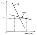
また例えば図6に示す従来の振動センサ回路100においては、ドライブ回路102の位相比較器102cのDC出力(制御電圧)を応力値信号(加速度信号)として利用することも考えられる。しかしながら、通常、電圧制御発振器102aにはLC共振器やCR共振器が用いられ、このような共振器を有する電圧制御発振器102aは、図4に示すように制御電圧Vcontに対する周波数変化量が大きい。即ち、周波数感度特性が高い。このため、従来の振動センサ回路100において共振周波数を検知結果とせずに、位相比較器102cの制御電圧Vcontを応力値信号(加速度信号)の検知結果として利用する場合は、周波数変化量に対する制御電圧Vcontの変化量が小さく検知感度が高いセンサを実現することができない。
これに対して、本実施形態の加速度検出装置1では、VCXO4の制御電圧を加速度信号として利用するようにしている。VCXO4は、制御電圧に対する周波数可変範囲がVCOに比べて狭い(周波数制御感度が低い)ため、加速動作に伴う周波数変化に対してLPF5の出力電圧(制御電圧)の変化を大電流化(高電位化)することができる。この結果、加速度変化に対して高感度センサを実現することができる。
In the present embodiment, the first and second tuning-fork type
For example, in the conventional
On the other hand, in the acceleration detection device 1 of the present embodiment, the control voltage of the VCXO 4 is used as an acceleration signal. Since VCXO4 has a narrow frequency variable range for the control voltage compared to the VCO (frequency control sensitivity is low), the change in the output voltage (control voltage) of the LPF 5 with respect to the frequency change accompanying the acceleration operation is increased (high potential). ). As a result, a highly sensitive sensor can be realized with respect to acceleration changes.
これまで説明した本実施形態では応力感応素子として音叉型水晶振動素子20を例に挙げて説明したが、これはあくまでも一例であり、応力感応素子として、例えば図5に示すような双音叉型水晶振動素子を用いることも可能である。
図5に示す双音叉型水晶振動素子23は、並列に配置された2本の振動腕21a、21bと、この2本の振動腕21a、21bの延長方向の両端を夫々結合した結合部22a、22bとから成る。そして、この場合は、例えば、結合部22a、22bの内、一方の結合部22aだけを、当該双音叉型水晶振動素子23が搭載される基板(図示しない)に固定し、他方を自由端とすればよい。
双音叉型水晶振動素子23を用いて本実施形態の加速度検出装置を構成した場合は、自由端側の結合部22bが重りとして機能するため、上記した音叉型水晶振動素子20より加速度感度を高めることができる。
なお、本実施形態では応力感応素子として音叉型振動素子を例に挙げて説明したが、これはあくまでも一例であり、共振周波数が加速度に応じて変化する素子であれば、所謂ATカットの水晶振動子やレゾネータといった各種圧電振動素子を応力感応素子として適用することも可能である。
In the present embodiment described so far, the tuning fork type crystal vibrating element 20 has been described as an example of the stress sensitive element. However, this is merely an example, and as the stress sensitive element, for example, a double tuning fork type crystal as shown in FIG. It is also possible to use a vibration element.
The double tuning fork type
When the acceleration detecting device of the present embodiment is configured using the double tuning fork type
In the present embodiment, a tuning fork type vibration element has been described as an example of the stress sensitive element. However, this is only an example, and so-called AT-cut crystal vibration is used as long as the resonance frequency changes according to acceleration. Various piezoelectric vibration elements such as a child and a resonator can be applied as a stress sensitive element.
1…加速度検出装置、2…発振回路、3…位相比較回路、4…VCXO、5…LPF、6…微分回路、7…バッファアンプ、8…DCサーボ回路、20…音叉型水晶振動素子、21a、21b…各振動腕、22、22a、22b…結合部、23…双音叉型水晶振動素子 DESCRIPTION OF SYMBOLS 1 ... Acceleration detection apparatus, 2 ... Oscillation circuit, 3 ... Phase comparison circuit, 4 ... VCXO, 5 ... LPF, 6 ... Differentiation circuit, 7 ... Buffer amplifier, 8 ... DC servo circuit, 20 ... Tuning fork type crystal vibration element, 21a , 21b, each vibrating arm, 22, 22a, 22b, a coupling portion, 23, a double tuning fork type crystal vibrating element
Claims (3)
第2の応力感応素子を共振子として備えた電圧制御型圧電発振回路と、
前記発振回路から出力される出力信号と前記電圧制御型圧電発振回路から出力される出力信号の位相を比較する位相比較回路と、
前記位相比較回路から出力される位相差信号の低域成分を抽出するローパスフィルタと、
前記ローパスフィルタから出力される出力信号を微分する微分回路と、
前記ローパスフィルタの出力信号に応じた制御電圧を前記電圧制御型圧電発振回路にフィードバックする直流サーボ回路と、を備え、
前記第1及び第2の応力感応素子は、加速度を検出する加速度検出軸方向を一致させ、且つ、前記第1及び第2の応力感応素子において検出する加速度検出方向が逆向きとなるように配置して、前記微分回路の出力信号を加速度検出信号として出力することを特徴とする加速度検出装置。 An oscillation circuit including a first stress sensitive element as a resonator;
A voltage-controlled piezoelectric oscillation circuit including a second stress-sensitive element as a resonator;
A phase comparison circuit for comparing the phase of the output signal output from the oscillation circuit and the output signal output from the voltage-controlled piezoelectric oscillation circuit;
A low pass filter for extracting a low frequency component of the phase difference signal output from the phase comparison circuit;
A differentiating circuit for differentiating an output signal output from the low-pass filter;
A DC servo circuit that feeds back a control voltage corresponding to the output signal of the low-pass filter to the voltage-controlled piezoelectric oscillation circuit,
The first and second stress sensitive elements are arranged so that the acceleration detection axis directions for detecting acceleration coincide with each other and the acceleration detection directions detected by the first and second stress sensitive elements are opposite to each other. Then, the acceleration detection device outputs the output signal of the differentiation circuit as an acceleration detection signal.
前記第1及び第2の音叉型振動素子は、それぞれ並列に配置された2本の振動腕と、該2本の振動腕の延長方向一端を結合する結合部とを有し、前記第1及び第2の音叉型振動素子の各振動腕の延長方向を加速度検出軸方向と一致させ、且つ、前記第1及び第2の音叉型振動素子を対向配置したことを特徴とする請求項1に記載の加速度検出装置。 The first and second stress sensitive elements are constituted by first and second tuning fork type vibration elements,
The first and second tuning-fork type vibration elements each include two vibrating arms arranged in parallel, and a coupling portion that couples one end in the extension direction of the two vibrating arms. 2. The extending direction of each vibrating arm of the second tuning-fork type vibration element is made to coincide with the acceleration detection axis direction, and the first and second tuning-fork type vibration elements are arranged to face each other. Acceleration detection device.
Priority Applications (1)
| Application Number | Priority Date | Filing Date | Title |
|---|---|---|---|
| JP2007022658A JP2008190884A (en) | 2007-02-01 | 2007-02-01 | Acceleration detector |
Applications Claiming Priority (1)
| Application Number | Priority Date | Filing Date | Title |
|---|---|---|---|
| JP2007022658A JP2008190884A (en) | 2007-02-01 | 2007-02-01 | Acceleration detector |
Publications (1)
| Publication Number | Publication Date |
|---|---|
| JP2008190884A true JP2008190884A (en) | 2008-08-21 |
Family
ID=39751137
Family Applications (1)
| Application Number | Title | Priority Date | Filing Date |
|---|---|---|---|
| JP2007022658A Withdrawn JP2008190884A (en) | 2007-02-01 | 2007-02-01 | Acceleration detector |
Country Status (1)
| Country | Link |
|---|---|
| JP (1) | JP2008190884A (en) |
-
2007
- 2007-02-01 JP JP2007022658A patent/JP2008190884A/en not_active Withdrawn
Similar Documents
| Publication | Publication Date | Title |
|---|---|---|
| US8875578B2 (en) | Electronic damper circuit for MEMS sensors and resonators | |
| EP2867613B1 (en) | Improved vibratory gyroscope | |
| KR101297654B1 (en) | Temperature compensation method and temperature and oscillation control loop system of parallel plate electrode type resonance sensor | |
| JP2015525872A5 (en) | ||
| EP2783222A1 (en) | Mems inertial sensor and method of inertial sensing | |
| US9252707B2 (en) | MEMS mass bias to track changes in bias conditions and reduce effects of flicker noise | |
| JP2002228453A (en) | Oscillatory gyro and temperature drift adjusting method therefor | |
| JP5187836B2 (en) | Sensor sensitivity adjusting means and sensor manufacturing method | |
| CN102906539B (en) | There is the angular-rate sensor of improvement ageing properties | |
| US7343802B2 (en) | Dynamic-quantity sensor | |
| JP5105345B2 (en) | Oscillator | |
| WO2001036910A1 (en) | Angular speed sensor | |
| JP2008190884A (en) | Acceleration detector | |
| JP2008190924A (en) | Acceleration detector | |
| JP5208063B2 (en) | Vibration type gyro sensor | |
| US20070277614A1 (en) | Vibration sensor | |
| JP2008151632A (en) | Acceleration detector | |
| JP2008157766A (en) | Acceleration detector | |
| CN107979351A (en) | A kind of coupling pressure drag MEMS oscillator based on high-order synchronization | |
| JP5589171B2 (en) | Circuit for physical quantity detection device | |
| JP2008256580A (en) | Acceleration detector | |
| JP2008157767A (en) | Acceleration detector | |
| JP2008170308A (en) | Acceleration detector | |
| JP2008151630A (en) | Acceleration detector | |
| JP2008170307A (en) | Acceleration detector |
Legal Events
| Date | Code | Title | Description |
|---|---|---|---|
| A300 | Application deemed to be withdrawn because no request for examination was validly filed |
Free format text: JAPANESE INTERMEDIATE CODE: A300 Effective date: 20100406 |