JP2008185970A - Pattern forming method, manufacturing method of electronic device, and electronic device - Google Patents
Pattern forming method, manufacturing method of electronic device, and electronic device Download PDFInfo
- Publication number
- JP2008185970A JP2008185970A JP2007021700A JP2007021700A JP2008185970A JP 2008185970 A JP2008185970 A JP 2008185970A JP 2007021700 A JP2007021700 A JP 2007021700A JP 2007021700 A JP2007021700 A JP 2007021700A JP 2008185970 A JP2008185970 A JP 2008185970A
- Authority
- JP
- Japan
- Prior art keywords
- pattern
- phase shift
- positive photoresist
- photoresist
- halftone phase
- Prior art date
- Legal status (The legal status is an assumption and is not a legal conclusion. Google has not performed a legal analysis and makes no representation as to the accuracy of the status listed.)
- Pending
Links
Images


Classifications
-
- G—PHYSICS
- G03—PHOTOGRAPHY; CINEMATOGRAPHY; ANALOGOUS TECHNIQUES USING WAVES OTHER THAN OPTICAL WAVES; ELECTROGRAPHY; HOLOGRAPHY
- G03F—PHOTOMECHANICAL PRODUCTION OF TEXTURED OR PATTERNED SURFACES, e.g. FOR PRINTING, FOR PROCESSING OF SEMICONDUCTOR DEVICES; MATERIALS THEREFOR; ORIGINALS THEREFOR; APPARATUS SPECIALLY ADAPTED THEREFOR
- G03F7/00—Photomechanical, e.g. photolithographic, production of textured or patterned surfaces, e.g. printing surfaces; Materials therefor, e.g. comprising photoresists; Apparatus specially adapted therefor
- G03F7/0035—Multiple processes, e.g. applying a further resist layer on an already in a previously step, processed pattern or textured surface
-
- G—PHYSICS
- G03—PHOTOGRAPHY; CINEMATOGRAPHY; ANALOGOUS TECHNIQUES USING WAVES OTHER THAN OPTICAL WAVES; ELECTROGRAPHY; HOLOGRAPHY
- G03F—PHOTOMECHANICAL PRODUCTION OF TEXTURED OR PATTERNED SURFACES, e.g. FOR PRINTING, FOR PROCESSING OF SEMICONDUCTOR DEVICES; MATERIALS THEREFOR; ORIGINALS THEREFOR; APPARATUS SPECIALLY ADAPTED THEREFOR
- G03F1/00—Originals for photomechanical production of textured or patterned surfaces, e.g., masks, photo-masks, reticles; Mask blanks or pellicles therefor; Containers specially adapted therefor; Preparation thereof
- G03F1/26—Phase shift masks [PSM]; PSM blanks; Preparation thereof
- G03F1/32—Attenuating PSM [att-PSM], e.g. halftone PSM or PSM having semi-transparent phase shift portion; Preparation thereof
-
- G—PHYSICS
- G03—PHOTOGRAPHY; CINEMATOGRAPHY; ANALOGOUS TECHNIQUES USING WAVES OTHER THAN OPTICAL WAVES; ELECTROGRAPHY; HOLOGRAPHY
- G03F—PHOTOMECHANICAL PRODUCTION OF TEXTURED OR PATTERNED SURFACES, e.g. FOR PRINTING, FOR PROCESSING OF SEMICONDUCTOR DEVICES; MATERIALS THEREFOR; ORIGINALS THEREFOR; APPARATUS SPECIALLY ADAPTED THEREFOR
- G03F1/00—Originals for photomechanical production of textured or patterned surfaces, e.g., masks, photo-masks, reticles; Mask blanks or pellicles therefor; Containers specially adapted therefor; Preparation thereof
- G03F1/68—Preparation processes not covered by groups G03F1/20 - G03F1/50
- G03F1/70—Adapting basic layout or design of masks to lithographic process requirements, e.g., second iteration correction of mask patterns for imaging
-
- Y—GENERAL TAGGING OF NEW TECHNOLOGICAL DEVELOPMENTS; GENERAL TAGGING OF CROSS-SECTIONAL TECHNOLOGIES SPANNING OVER SEVERAL SECTIONS OF THE IPC; TECHNICAL SUBJECTS COVERED BY FORMER USPC CROSS-REFERENCE ART COLLECTIONS [XRACs] AND DIGESTS
- Y10—TECHNICAL SUBJECTS COVERED BY FORMER USPC
- Y10T—TECHNICAL SUBJECTS COVERED BY FORMER US CLASSIFICATION
- Y10T428/00—Stock material or miscellaneous articles
- Y10T428/24—Structurally defined web or sheet [e.g., overall dimension, etc.]
- Y10T428/24273—Structurally defined web or sheet [e.g., overall dimension, etc.] including aperture
-
- Y—GENERAL TAGGING OF NEW TECHNOLOGICAL DEVELOPMENTS; GENERAL TAGGING OF CROSS-SECTIONAL TECHNOLOGIES SPANNING OVER SEVERAL SECTIONS OF THE IPC; TECHNICAL SUBJECTS COVERED BY FORMER USPC CROSS-REFERENCE ART COLLECTIONS [XRACs] AND DIGESTS
- Y10—TECHNICAL SUBJECTS COVERED BY FORMER USPC
- Y10T—TECHNICAL SUBJECTS COVERED BY FORMER US CLASSIFICATION
- Y10T428/00—Stock material or miscellaneous articles
- Y10T428/24—Structurally defined web or sheet [e.g., overall dimension, etc.]
- Y10T428/24802—Discontinuous or differential coating, impregnation or bond [e.g., artwork, printing, retouched photograph, etc.]
Abstract
Description
本発明は、パターンの形成方法、電子デバイスの製造方法および電子デバイスに関し、特に、微小孤立ホールパターンを有するランダム配置ホールパターンの形成方法、電子デバイスの製造方法および電子デバイスに関するものである。 The present invention relates to a pattern forming method, an electronic device manufacturing method, and an electronic device, and more particularly to a random arrangement hole pattern forming method having a minute isolated hole pattern, an electronic device manufacturing method, and an electronic device.
光リソグラフィにおける、ホールパターン形成ではラインパターンと異なり、2次元的に電磁場を局在させる必要があるので、微細化が原理的に困難である。さらに、ホールパターンをポジ型フォトレジストにより形成する場合には、像の実効コントラストが本質的に小さくなる。 Unlike the line pattern, hole pattern formation in photolithography requires the electromagnetic field to be localized two-dimensionally, so that miniaturization is difficult in principle. Furthermore, when the hole pattern is formed of a positive photoresist, the effective contrast of the image is essentially reduced.
なかでも、微小孤立ホールの形成には、有効な超解像技術がないので、その高プロセス余裕下での形成は難しい。このため、微小孤立ホールの形成はデバイスの微細化を抑制する要因の一つとなっている。 In particular, since there is no effective super-resolution technique for forming minute isolated holes, it is difficult to form them with a high process margin. For this reason, the formation of minute isolated holes is one of the factors that suppress the miniaturization of devices.
一方、規則的に配置されたホールパターンにおいては、上記した原理的制約により、形成される光学像の像質は一次元パターンである密集ラインパターンと比べて劣る。しかし、変形照明法に代表される超解像技術が存する。このため、優れた分離性能をもつ高解像フォトレジストの適用により、高プロセス裕度での高密集微細ホールの形成が可能である。 On the other hand, in the regularly arranged hole patterns, the image quality of the formed optical image is inferior to that of the dense line pattern which is a one-dimensional pattern due to the above-mentioned principle restrictions. However, there is a super-resolution technique represented by the modified illumination method. For this reason, the application of a high-resolution photoresist having excellent separation performance makes it possible to form highly dense fine holes with a high process margin.
他方、暗点像の形成においては、本件の発明者が開示しているように(特許文献1および非特許文献1参照)、最適変形照明下での位相シフトマスクによる位相打消し像を適用することで、ランダムな配置のパターンにおいて優れた像質が得られる。
従来の位相シフトマスクによる位相反転像を適用したランダム配置のホールパターン形成では、上記したようにネガ型フォトレジストが必要となる。しかしながら、現状の最先端技術であるArFエキシマレーザー露光においては、優れた特性のネガ型フォトレジストは存在しない。このため、従来の方法においては、ArFエキシマレーザー波長においては実用に十分な特性を得ることが難しいという問題点があった。 In forming a hole pattern in a random arrangement using a phase-inverted image by a conventional phase shift mask, a negative photoresist is required as described above. However, in ArF excimer laser exposure, which is the current state-of-the-art technology, there is no negative photoresist having excellent characteristics. For this reason, the conventional method has a problem that it is difficult to obtain characteristics sufficient for practical use at an ArF excimer laser wavelength.
本発明は、上記の課題に鑑みてなされたものであり、その目的は、ポジ型のフォトレジスト適用下で、ランダム配置のホールパターンを、高裕度で形成することができるパターンの形成方法、電子デバイスの製造方法および電子デバイスを提供することである。 The present invention has been made in view of the above-described problems, and its object is to provide a pattern forming method and an electron that can form a randomly arranged hole pattern with high tolerance under application of a positive photoresist. A device manufacturing method and an electronic device are provided.
本発明の実施の形態におけるパターンの形成方法は以下の工程を備えている。
まず被加工膜上に、第1のポジ型フォトレジストを適用したパターン形成により、複数のホールパターンが密集した密集ホールパターンを有するマスク層が形成される。密集ホールパターンの複数のホールパターンの各々を埋め込むようにマスク層上に第2のポジ型フォトレジストが形成される。第2のポジ型フォトレジストにハーフトーン位相シフトマスクを用いて暗点像が投影され露光される。露光された第2のポジ型フォトレジストを現像することにより、第2のポジ型フォトレジストの暗点像部分に形成されるドットパターンがマスク層の複数のホールパターンのいずれかの内部に残される。マスク層と第2のポジ型フォトレジストにより形成されたドットパターン(レジストプラグ)とをマスクとして、被加工膜がパターニングされる。ハーフトーン位相シフトマスクは、ドットパターン用の暗点像を生成する開口部を有するハーフトーン位相シフト膜を有している。第2のポジ型フォトレジストにハーフトーン位相シフトマスクを用いて暗点像を投影し露光する工程は、開口部の存在しない領域でハーフトーン位相シフト膜を透過した露光光の光強度では第2のポジ型フォトレジストが現像時に溶解され、かつ開口部によりドットパターン部分に形成される暗点像の光強度では第2のポジ型フォトレジストが現像時に溶解されないような露光量で露光する工程を含む。
The pattern forming method according to the embodiment of the present invention includes the following steps.
First, a mask layer having a dense hole pattern in which a plurality of hole patterns are densely formed is formed on the film to be processed by pattern formation using the first positive photoresist. A second positive photoresist is formed on the mask layer so as to fill each of the plurality of hole patterns of the dense hole pattern. A dark spot image is projected onto the second positive photoresist using a halftone phase shift mask and exposed. By developing the exposed second positive photoresist, a dot pattern formed in the dark spot image portion of the second positive photoresist is left inside any of the plurality of hole patterns in the mask layer. . The film to be processed is patterned using the mask layer and the dot pattern (resist plug) formed by the second positive photoresist as a mask. The halftone phase shift mask has a halftone phase shift film having an opening for generating a dark spot image for a dot pattern. The step of projecting and exposing a dark spot image on the second positive photoresist using the halftone phase shift mask is the second in the light intensity of the exposure light transmitted through the halftone phase shift film in the region where no opening exists. And a step of exposing the second positive photoresist at an exposure amount so that the second positive photoresist is not dissolved at the time of development with the light intensity of the dark spot image formed in the dot pattern portion by the opening. Including.
本発明の実施の形態によれば、マスク層に密集ホールパターンが形成されるが、これはポジ型のフォトレジストを用いて行うことができる。また、平面視においてランダムな配置を有するドットパターンの形成もポジ型のフォトレジストを用いて行うことができる。このため、マスク層に密集ホールパターンを形成した後に、その密集ホールパターンのいずれかのホールパターンをドットパターンで埋め込むことで、平面視においてランダムな配置を有するホールパターンをポジ型のフォトレジストを用いて形成することが可能となる。よって、ポジ型のレジスト適用下で、ランダム配置のホールパターンを、高裕度で形成することができる。 According to the embodiment of the present invention, a dense hole pattern is formed in the mask layer, which can be performed using a positive photoresist. Further, a dot pattern having a random arrangement in a plan view can be formed using a positive photoresist. For this reason, after forming a dense hole pattern in the mask layer, a hole pattern having a random arrangement in a plan view is used by embedding one of the dense hole patterns with a dot pattern. Can be formed. Therefore, it is possible to form a randomly arranged hole pattern with high tolerance under the application of a positive resist.
以下、本発明の実施の形態について図に基づいて説明する。
(実施の形態1)
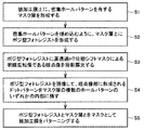
図1は、本発明の実施の形態1〜4に共通のパターンの形成方法を示すフロー図である。図1を参照して、本実施の形態のパターン形成方法においては、まず被加工膜上に、密集ホールパターンを有するマスク層が形成される(ステップS1)。この密集ホールパターンを埋め込むように、マスク層上にポジ型フォトレジストが形成される(ステップS2)。ポジ型フォトレジストに高透過ハーフトーン(HT)位相シフトマスクによる明暗反転像である暗点像が投影露光される(ステップS3)。この明暗反転像である暗点像を形成できる高透過ハーフトーン位相シフトマスクの構成については後述する。露光されたポジ型フォトレジストが現像される。これにより、暗点像部に形成されるドットパターン部分以外のポジ型フォトレジストが除去される。またドットパターン部分のポジ型フォトレジストが、密集パターンをなす複数のホールパターンのいずれかの内部に残存しレジストプラグとなる(ステップS4)。このポジ型フォトレジストとマスク層とをマスクとして被加工膜が選択的に除去されてパターニングされる(ステップS5)。これにより、被加工膜に平面視においてランダムな配置を有するホールパターンが形成される。
Hereinafter, embodiments of the present invention will be described with reference to the drawings.
(Embodiment 1)
FIG. 1 is a flowchart showing a pattern forming method common to the first to fourth embodiments of the present invention. Referring to FIG. 1, in the pattern forming method of the present embodiment, a mask layer having a dense hole pattern is first formed on a film to be processed (step S1). A positive photoresist is formed on the mask layer so as to embed this dense hole pattern (step S2). A dark spot image, which is a bright / dark reversal image using a high transmission halftone (HT) phase shift mask, is projected and exposed on the positive photoresist (step S3). The configuration of a high transmission halftone phase shift mask capable of forming a dark spot image which is a bright / dark inverted image will be described later. The exposed positive photoresist is developed. Thereby, the positive photoresist other than the dot pattern portion formed in the dark spot image portion is removed. Further, the positive photoresist in the dot pattern portion remains inside any one of the plurality of hole patterns forming the dense pattern to form a resist plug (step S4). Using this positive photoresist and mask layer as a mask, the film to be processed is selectively removed and patterned (step S5). Thereby, a hole pattern having a random arrangement in a plan view is formed in the film to be processed.
次に、上記におけるマスク層がポジ型のフォトレジストである場合について具体的に説明する。 Next, the case where the mask layer is a positive type photoresist will be specifically described.
図2は、マスク層がポジ型のフォトレジストである場合の図1のステップS1を具体的に示したフロー図である。また図3〜図11は、本発明の実施の形態1におけるパターンの形成方法を工程順に示す概略断面図である。 FIG. 2 is a flowchart specifically showing step S1 of FIG. 1 when the mask layer is a positive photoresist. 3 to 11 are schematic cross-sectional views showing the pattern forming method according to the first embodiment of the present invention in the order of steps.
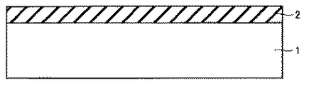
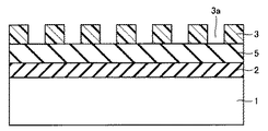
図3を参照して、まず、基板(たとえばウエハなど)1上に被加工膜2が形成される。
図4を参照して、被加工膜2上に、第1のポジ型のフォトレジスト3が塗布形成される(ステップS11:図2)。このとき、図示していないが、必要に応じて下層反射防止膜(BARC)および上層反射防止膜(TARC)が第1のポジ型フォトレジスト3の下層膜、上層膜として形成される。
Referring to FIG. 3, first, a film to be processed 2 is formed on a substrate (for example, a wafer) 1.
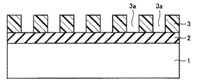
Referring to FIG. 4, first
図5を参照して、第1の露光プロセスが行われる。密集ホールパターンを形成したハーフトーン位相シフトマスク20の光学像が、4重極照明を適用した投影光学系により第1のポジ型フォトレジスト3に投影され、第1のポジ型フォトレジスト3が露光される(ステップS12:図2)。本実施の形態では、露光波長(λ)はたとえば193nmであり、開口数(NA)がたとえば1.07の液浸露光系が適用される。
Referring to FIG. 5, the first exposure process is performed. The optical image of the halftone
なおハーフトーン位相シフトマスク20は、透明基板11とハーフトーン位相シフト膜12とを有している。透明基板11は、露光光を透過するように露光光に対して透明な材質よりなっている。ハーフトーン位相シフト膜12は、透明基板11上に形成され、かつ透明基板の一部表面を露出する開口部12aを複数個有している。このハーフトーン位相シフト膜12は、そのハーフトーン位相シフト膜12を透過した露光光の位相が開口部12aを透過した露光光の位相と異なる位相(たとえば180°異なる位相)となるように構成されている。また、波長に比べて大きい開口部を透過した露光光の光強度に対するハーフトーン位相シフト膜12を透過した露光光の光強度、すなわちハーフトーン位相シフト膜12の透過率は適宜設定されてもよく、たとえば20%程度であってもよい。
The halftone
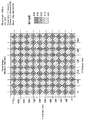
この複数の開口部12aは、図12に示すように平面視において複数の縦線と複数の横線とが直交に交差する直交格子(例えば正方格子)を仮想したときに、複数の縦線と複数の横線とが交差する複数の交点の各々に規則正しく配置され、それにより密集ホールパターンを構成している。
As shown in FIG. 12, the plurality of
図6を参照して、上記において密集ホールパターンの光学像が露光された第1のポジ型フォトレジスト3が現像される。これにより、第1のフォトレジスト3に複数個のホールパターン3aが形成される。この複数のホールパターン3aの各々は、配置ピッチがたとえば160nm、直径がたとえば60nmとなるように規則的に配置されることで密集ホールパターンを構成している(ステップS13:図2)。ここには図示しなかったが、前記したBARC膜、TARC膜を適用した場合、現像後にBARC膜はそのまま残存する。この残存したBARC膜は、後で示す第2の露光プロセスでもBARCとして働く。なおTARC膜は第1のフォトレジスト3の現像時もしくは現像前の処理により溶解除去される。
Referring to FIG. 6, first
この後、第1のフォトレジスト3から残存溶媒を揮散させることで第1のフォトレジスト3を固化させるハードニング処理が行われる。このハードニング処理は、第2の露光プロセスにおいて第1のフォトレジスト3上に塗布形成される他の第2のフォトレジスト4が第1のフォトレジスト3と交じり合うことで、均一な膜形成が阻害されることを回避するために行われる。通常、このハードニング処理は、第1のフォトレジスト3への紫外光の照射、もしくは、電子線の照射、希ガスイオンの注入などにより行われる。本実施の形態においては、たとえば紫外光を照射することによりこのハードニング処理が行なわれる。
Thereafter, a hardening process for solidifying the
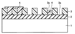
図7を参照して、ハードニング処理をされた第1のフォトレジスト3の上に、複数のホールパターン3aの各々を埋め込むように、他の第2のポジ型フォトレジスト4が塗布形成される(ステップS2:図1)。このとき、図示していないが、必要に応じて下層反射防止膜(BARC)および上層反射防止膜(TARC)が第2のフォトレジスト4の下層膜、上層膜として形成される。本実施の形態では、第1のフォトレジスト3の下層膜として形成したBARC膜が第2のフォトレジスト4の塗布時にそのまま残っているので、この第2のフォトレジスト4の形成工程ではBARC膜は形成されない。TARC膜は精密なパターン形成に必要であるので、この第2のフォトレジスト4の上層膜として形成される。
Referring to FIG. 7, another second
図8を参照して、第2の露光プロセスが行われる。ランダム配置ホールパターンを形成した高透過ハーフトーン位相シフトマスク30の光学像が、クロスポール照明を適用した投影光学系により第2のポジ型フォトレジスト4に投影され、第2のフォトレジスト4が露光される(ステップS3:図1)。本実施の形態では、露光波長(λ)はたとえば193nmであり、開口数(NA)がたとえば1.07の液浸露光系が適用される。
Referring to FIG. 8, the second exposure process is performed. The optical image of the high-transmission halftone
なお高透過ハーフトーン位相シフトマスク30は、透明基板21とハーフトーン位相シフト膜22とを有している。透明基板21は、露光光を透過するように露光光に対して透明な材質よりなっている。ハーフトーン位相シフト膜22は、透明基板21上に形成され、かつ透明基板21の一部表面を露出する開口部22aを1個もしくは複数個有している。このハーフトーン位相シフト膜22は、そのハーフトーン位相シフト膜22を透過した露光光の位相が開口部22aを透過した露光光の位相と異なる位相(たとえば180°異なる位相)となるように構成されている。また、波長に比べて十分に大きい開口部を透過した露光光の光強度に対するハーフトーン位相シフト膜を透過した露光光の光強度が15%以上25%以下である。開口部22aの寸法Wは、露光光の波長λ/開口数NAを1とした計測で0.26以上0.45以下であり、好ましくは0.32以上0.39以下である。
The high transmission halftone
ここで、開口部22aの寸法Wとは、開口部22aの平面形状が矩形状である場合にはその矩形の1辺の寸法を意味する。
Here, the dimension W of the
この1個もしくは複数個の開口部22aは、図13に示すように平面視において複数の縦線と複数の横線とが直交に交差する直交格子(例えば正方格子)を仮想したときに、複数の縦線と複数の横線とが交差する複数の交点のいずれかにランダムに配置され、それによりランダム配置ホールパターンを構成している。また図13における仮想の格子は図12における仮想の格子に一致している。このため、図13に示す開口部22aの位置は図12に示す複数のホールパターン12aのいずれかの位置に一致する。
As shown in FIG. 13, the one or a plurality of
この高透過ハーフトーン位相シフトマスク30を用いた露光においては、ハーフトーン位相シフト膜22の開口部22aの明暗反転像である暗点像が第2のフォトレジスト4に投影される。つまり、通常のハーフトーン位相シフトマスクにおいては、開口部の形成された領域が明部となり、ハーフトーン位相シフト膜の形成された領域が暗部となる。これに対して、この高透過ハーフトーン位相シフトマスク30では、開口部22aの形成された領域が暗部となり、高透過ハーフトーン位相シフト膜22の形成された領域が明部となる。
In exposure using the high transmission halftone
このため露光量を適当に設定することで、開口部22aにより形成される暗点像の光強度は第2のポジ型フォトレジスト4を現像時に溶解しないような光強度となる。また、高透過ハーフトーン位相シフト膜22の波長に比べて大きい形成領域部を透過した露光光の光強度は第2のポジ型フォトレジスト4を現像時に溶解するような光強度となる。
For this reason, by setting the exposure amount appropriately, the light intensity of the dark spot image formed by the
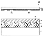
図9を参照して、上記においてランダム配置の暗点像が露光された第2のポジ型フォトレジスト4が現像されて、暗点像部分のレジストがドットパターンとして残存する。これにより、第2のフォトレジスト4のドットパターン部分が第1のフォトレジスト3の複数のホールパターン3aのいずれかの内部を埋め込む。ドットパターン部4がホールパターン3a内を埋め込むことで、平面視においてランダムに配置されたホールパターンを得ることができる。
Referring to FIG. 9, the second
図10を参照して、フォトレジスト3、4をマスクとして被加工膜2がエッチングにより選択除去される。この後、フォトレジスト3、4がたとえばアッシングなどにより除去される。
Referring to FIG. 10,
図11を参照して、上記のエッチングにより、平面視においてランダムに配置されたホールパターン2aが被加工膜2に形成されて、本実施の形態のパターンが形成される。このように形成されるパターンは電子デバイスに適用され得る。
Referring to FIG. 11,
次に、上記パターンの形成方法における第1および第2の露光プロセスに用いられる投影露光装置について説明する。 Next, a projection exposure apparatus used for the first and second exposure processes in the pattern forming method will be described.
図14は、本発明の実施の形態1における第1および第2の露光プロセスに用いられる投影露光装置の構成を概念的に示す図であり、特に第2の露光プロセスの場合を例示している。図14を参照して、この投影露光装置は、フォトマスク30(または20)上のパターンを基板1上の第2のフォトレジスト4に投射するものである。また投影露光装置は、光源111からフォトマスク30(または20)のパターンまでの照明光学系と、フォトマスク30(または20)のパターンから基板1までの投影光学系とを有している。
FIG. 14 is a diagram conceptually showing the configuration of the projection exposure apparatus used in the first and second exposure processes in the first embodiment of the present invention, and particularly exemplifies the case of the second exposure process. . Referring to FIG. 14, this projection exposure apparatus projects a pattern on photomask 30 (or 20) onto
照明光学系は、光源111と、反射鏡112と、集光レンズ118と、フライアイレンズ113と、変形照明用の絞り114と、集光レンズ116a、116b、116cと、ブラインド絞り115と、反射鏡117とを有している。また投影光学系は投影レンズ119a、119bと、瞳面絞り125とを有している。
The illumination optical system includes a
その露光動作においては、まず光源111から発せられた光111aは、反射鏡112により反射される。次に、光111aは、集光レンズ118を通過して、フライアイレンズ113の各フライアイ構成レンズ113aの各々に入射し、その後に絞り114を通過する。
In the exposure operation, light 111 a emitted from the
ここで、光111bは、1個のフライアイ構成レンズ113aによって作り出された光路を示し、光111cはフライアイレンズ113によって作り出される光路を示している。絞り114を通過した光111aは、集光レンズ116a、ブラインド絞り115および集光レンズ116bを通過して、反射鏡117により所定角度で反射される。
Here, the light 111b indicates an optical path created by one fly-eye component lens 113a, and the light 111c indicates an optical path created by the fly-
反射鏡117により反射された光111aは、集光レンズ116cを透過した後、所定のパターンが形成されたフォトマスク30(または20)の全面を均一に照射する。この後、光111aは投影レンズ119a、119bにより所定の倍率に縮小され、基板1上の第2のフォトレジスト4を露光する。
The light 111a reflected by the reflecting
本実施の形態においては、第1および第2の露光プロセスの双方において位相シフトマスク30(または20)の照明は通常照明ではなく、変形照明により行なわれる。通常照明の場合、図15に示すように位相シフトマスク30(または20)に対して露光光が垂直に照射され、0次光および±1次光の3光束によりウエハ10のフォトレジストが露光される。しかし、位相シフトマスク30(または20)のパターンが微細になると、回折角度が大きくなるため、垂直照明では±1次光がレンズの中に入らなくなり、解像しなくなるおそれがある。
In the present embodiment, illumination of the phase shift mask 30 (or 20) is performed not by normal illumination but by modified illumination in both the first and second exposure processes. In the case of normal illumination, as shown in FIG. 15, the exposure light is irradiated perpendicularly to the phase shift mask 30 (or 20), and the photoresist on the
そこで、図16に示すように変形照明により照明光束が位相シフトマスク30(または20)に対して斜めに入射される。これにより、位相シフトマスク30(または20)により回折した0次光と+1次光あるいは−1次光の2光束のみで露光することができ、解像性を得ることができる。 Therefore, as shown in FIG. 16, the illumination light beam is incident obliquely on the phase shift mask 30 (or 20) by the modified illumination. As a result, exposure can be performed with only two light beams of 0th order light and + 1st order light or −1st order light diffracted by the phase shift mask 30 (or 20), and resolution can be obtained.
本実施の形態の第2の露光プロセスの変形照明としてはクロスポール照明が用いられる。つまり、図17に示すように4つの透過部114aを有するクロスポール照明絞り114が図14の絞り114として用いられる。また本実施の形態の第1の露光プロセスの変形照明として4重極照明が用いられる。つまり、図18に示すように4つの透過部114aを有し、かつクロスポール照明を45°回転した形状を有する4重極照明絞り114が図18の絞り114として用いられる。
Cross pole illumination is used as modified illumination in the second exposure process of the present embodiment. That is, as shown in FIG. 17, a cross
次に、本実施の形態におけるパターン形成方法によって得られるパターンを有する電子デバイスの構造について説明する。 Next, the structure of an electronic device having a pattern obtained by the pattern forming method in the present embodiment will be described.
図19は、本発明の実施の形態1における電子デバイスの構成を概略的に示す平面図である。図11の断面図は、図19のXI−XI線に沿う断面に対応している。図11および図19を参照して、本実施の形態の電子デバイスは、基板1と、その基板1上に形成された被加工膜2とを有している。被加工膜2には、平面視においてランダムに配置された複数のホールパターン2aが形成されている。この複数のホールパターン2aは、平面視において複数の縦線51と複数の横線52とが直交交差する直交格子(たとえば正方格子)を仮想したときに、その複数の縦線51と複数の横線52とが交差する複数の交点53のうち任意の交点53に配置されている。このホールパターン2aの平面的な寸法(直径)はたとえば60〜70nmである。
FIG. 19 is a plan view schematically showing the configuration of the electronic device according to
次に、図8に示す高透過ハーフトーン位相シフトマスク30を用いることにより、パターンの明暗反転像が得られる点について説明する。尚、本説明では露光波長を248nmとしており本実施の形態での193nmと異なるが、物理現象は波長に依存しないので現象としては193nmでも同様であることを、ここに付記する。
Next, a description will be given of the fact that a bright and dark inverted image of a pattern can be obtained by using the high transmission halftone
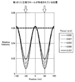
図20〜図23は、図8に示す高透過ハーフトーン位相シフトマスク30の開口部22aを孤立パターンとし、その孤立パターン22aの寸法Wに対して結像系により形成される光学像の変化を示す図である。各グラフでのパラメータはフォーカスである。光学条件として、露光光の波長は248nm、開口数NAは0.80、照明はクロスポール照明(σin/σout=0.70/0.85)である。そのクロスポール照明の絞り14の形状は図17に示すような4つの光透過部114aを有する形状である、また、位相シフトマスク30の透過率(I2/I1)は20%である。
20 to 23 show changes in the optical image formed by the imaging system with respect to the dimension W of the
高透過ハーフトーン位相シフトマスク30の開口部22aの寸法Wが大きいときには、従来のハーフトーン型位相シフトマスクによるパターン形成の場合にほぼ対応する。この場合、図20に示すように開口部22aの透過光の強度が、それを打ち消す位相関係となるハーフトーン位相シフト膜22の透過光の強度に比べ十分に大きくなる。このため、開口部22aに対応する領域では、他の領域よりも明るい部分(光強度の高い部分)が形成される。
When the dimension W of the
開口部22aの寸法Wを小さくしていくと、図21に示すように開口部22aの透過光の強度が小さくなっていき、ハーフトーン位相シフト膜22の透過光による打消しが相対的に大きくなる。これにより、ハーフトーン位相シフト膜22の透過光の強度とほぼ同じ強度の像が形成されるようになる。このときは、像のコントラストが小さく、フォトレジストにパターンを形成することが困難となる。
As the dimension W of the
さらに開口部22aの寸法Wを小さくしていくと、開口部22aの透過光強度とハーフトーン位相シフト膜22の透過光強度とがほぼ等しくなる。このとき、相互の位相が反位相の関係(つまり位相が180°異なる関係)となっているので、図22に示すように、開口部22aに対応する領域では、他の領域よりも十分暗い暗点像が形成される。つまり、ハーフトーン位相シフト膜22のパターンの明暗反転像が得られることになる。この像をポジ型のフォトレジストに適用すれば、フォトレジストにドットパターンが形成されることになる。
When the dimension W of the
さらに開口部22aの寸法Wを小さくしていくと、図23に示すように、今度は開口部22aを透過した光の強度が、ハーフトーン位相シフト膜22の透過光の強度より小さくなり、打ち消しによる効果が小さくなることで、暗点の暗さが弱く(明るく)なっていく。
When the dimension W of the
さらに開口部22aの寸法Wを小さくしていくと、開口部22aが存在しないのと実質的に同じとなり、像のコントラストがなくなっていく。
When the dimension W of the
このように、上記の光学条件においては、図22に示すような明暗反転像が得られ、さらに明暗反転像における暗点像が優れたフォーカス特性を示すことがわかる。また、このような明暗反転像を得るためには、開口部22aを透過した露光光の光強度に対するハーフトーン位相シフト膜22を透過した露光光の光強度の比により定義される光透過率が15%以上25%以下であることが必要がある。加えて、開口部22aの寸法Wが、露光光の波長λ/開口数NAを1とした計測で0.26以上0.45以下であることが必要であり、0.32以上0.39以下であることが好ましい。このことは特開2004−251969号公報に記載されている。
Thus, it can be seen that, under the above optical conditions, a bright / dark inverted image as shown in FIG. 22 is obtained, and a dark spot image in the bright / dark inverted image shows excellent focus characteristics. Further, in order to obtain such a light / dark inverted image, the light transmittance defined by the ratio of the light intensity of the exposure light transmitted through the halftone
次に、第1および第2の露光プロセスにおける光学像を調べた結果について説明する。
図24は、第1の露光プロセスにおいて、20%透過ハーフトーン位相シフトマスク20に形成された、ピッチ160nmで2次元に密集配置された112nm□のホールパターンを結像した光学像の強度分布を示す等高線図である。光学条件として、露光光の波長は193nm、開口数NAは1.07、照明は4重極照明(σin/σout=0.85/0.95)である。また図25は、第1の露光プロセスにおける密集ホールの主断面に沿った位置(Spatial Position)における光強度(Relative Intensity)の分布を、フォーカスをパラメータとして示した図である。図24および図25を参照して、第1の露光プロセスにおいて得られる光学像はレジストの解像に十分なコントラストを有しており、フォーカスによる変化が小さく優れたフォーカス特性を有している。この光学像の特性より、ピッチ160nmで直径〜60nmの密集ホールパターンが第1のフォトレジスト3に高裕度で形成されることがわかる。
Next, the result of examining the optical image in the first and second exposure processes will be described.
FIG. 24 shows an intensity distribution of an optical image formed by imaging a 112 nm square hole pattern formed in the 20% transmission halftone
また図26は、第1の露光プロセスで形成される明点像の寸法すなわちImage CD(Critical Dimension)をフォーカスに対してプロットした図であり、スライスレベル(露光量に反比例する量)をパラメータとして示した図である。図26を参照して、第1の露光プロセスにおいてはデフォーカスによるCD値の変動が少なく、優れたフォーカス特性が得られることが分かる。 FIG. 26 is a diagram in which the dimensions of the bright spot image formed in the first exposure process, that is, Image CD (Critical Dimension) is plotted with respect to the focus, and the slice level (a quantity inversely proportional to the exposure dose) is used as a parameter. FIG. Referring to FIG. 26, it can be seen that in the first exposure process, the CD value fluctuates due to defocusing and excellent focus characteristics can be obtained.
また図27は、第2の露光プロセスにおいて、20%透過ハーフトーン位相シフトマスク30に形成された62nm□のホールパターンを結像した光学像の強度分布を示す等高線図である。光学条件として、露光光の波長は193nm、開口数NAは1.07、照明はクロスポール照明(σin/σout=0.60/0.80)である。この62nm□のホールパターンは、第1のフォトレジスト3に形成された複数のホールパターンの一部の位置に対応して配置されている。図27を参照して、この光学像では20%透過ハーフトーン位相シフトマスク30上のホールパターンに対応する部分が、位相打消しにより暗点像となっている。
FIG. 27 is a contour diagram showing the intensity distribution of an optical image formed by imaging a 62 nm □ hole pattern formed on the 20% transmission halftone
この暗点像により、その部分の第2のポジ型フォトレジスト4が現像時に非溶解となることで、現像後にこの部分(ドットパターン部分)の第2のフォトレジスト4が残存する。これにより、下地であるフォトレジスト3に形成された複数のホールパターンの一部が、この第2のフォトレジスト4のドットパターン部分によりプラグされる。これが、第2の露光プロセスの役割である。
Due to this dark spot image, the second
また図28は、第2の露光プロセスにおいて、20%透過ハーフトーン位相シフトマスク30に形成された62nm□のホールパターンを、上記した光学条件下で結像した光学像の強度分布を示す等高線図である。この62nm□のホールパターンは、第1のフォトレジスト3に形成された複数のホールパターンのうち1個のホールパターンを除いた全てのホールパターンの位置に対応して配置されている。図28を参照して、この光学像では20%透過ハーフトーン位相シフトマスク30上のホールパターンに対応する部分が、位相打消しにより暗部となっており、マスク30上のホールパターンのない部分は明部となっている。すなわち、このマスク30を用いた第2のフォトレジスト4のパターニングでは、第1のフォトレジスト3に形成された密集ホールパターンのうち、1個を除いた全てのホールパターンが、暗点像により形成される第2のフォトレジスト4のドットパターンによりプラグされる。これにより、被加工膜2に孤立ホールパターンを形成することができる。
FIG. 28 is a contour map showing the intensity distribution of an optical image obtained by imaging the 62 nm □ hole pattern formed on the 20% transmission halftone
図29および図30は、第2の露光プロセスに用いられるマスクのホール非存在部分(図29)および孤立ホール存在部分(図30)の光学像の強度をフォーカスをパラメータにプロットした図である。図中にレジストの溶解・非溶解の境界となる像強度(スライスレベル:露光量によりその大きさは調整される)を破線で示している。 29 and 30 are plots of the optical image intensity of the hole non-existing portion (FIG. 29) and the isolated hole existing portion (FIG. 30) of the mask used in the second exposure process, with focus as a parameter. In the drawing, the image intensity (slice level: the size of which is adjusted by the exposure amount) serving as a boundary between dissolution and non-dissolution of the resist is indicated by a broken line.
図29および図30を参照して、ホール非存在部分におけるドットパターン部(プラグ形成部)および孤立ホール存在部分におけるドットパターン部(プラグ形成部)のどちらも、レジスト解像に十分な暗さになっている。また、フォーカスによる光強度の変化も小さい。すなわち、この光学像を露光することで、十分なプロセス裕度を有するドットパターンの形成が可能であると予測される。また、孤立ホール存在部分におけるホールパターン部では、第2のフォトレジスト4を感光させるに十分な強度を持った明点像が形成されている。
Referring to FIGS. 29 and 30, both the dot pattern portion (plug forming portion) in the hole non-existing portion and the dot pattern portion (plug forming portion) in the isolated hole existing portion are sufficiently dark for resist resolution. It has become. Also, the change in light intensity due to focus is small. That is, it is predicted that a dot pattern having a sufficient process tolerance can be formed by exposing this optical image. In the hole pattern portion in the isolated hole existing portion, a bright spot image having a sufficient intensity to expose the
以上より本実施の形態によれば、第1の露光プロセスにおいてハーフトーン位相シフトマスク20と変形照明により第1のポジ型フォトレジスト3に密集ホールパターンを形成することができる。この後、第2の露光プロセスにおいて、高透過ハーフトーン位相シフトマスク30とクロスポール照明により形成されるランダム配置の暗点像により、上記第1の露光プロセスにより形成された密集ホールパターンの任意の一部のホールパターン3a内を第2のフォトレジスト4によるドットパターンで埋め込むことができる。これにより、ランダム配置のホールパターンを形成することができる。このため、従来の方法では不可能であった、微細な寸法をもつ、ピッチが極めて小さい密集ホールパターンと孤立ホールパターンを含むランダム配置パターンの同時形成が可能となる。
As described above, according to the present embodiment, a dense hole pattern can be formed in the first
(実施の形態2)
本実施の形態においては、図5に示す第1の露光プロセスにおいて変形照明として図17に示すクロスポール照明を用いる点で実施の形態1と異なっている。このクロスポール照明を第1の露光プロセスに用いる場合には、図5に示すハーフトーン位相シフトマスク20の密集ホールパターンにおけるホールパターン12aの配置ピッチP1はたとえば120nmであり、平面寸法はたとえば88nm□である。また、このハーフトーン位相シフトマスク20を用いて形成された第1のフォトレジスト3の密集ホールパターンにおけるホールパターン3aの配置ピッチはたとえば120nmであり、直径はたとえば60nmである。
(Embodiment 2)
The present embodiment is different from the first embodiment in that the cross pole illumination shown in FIG. 17 is used as the modified illumination in the first exposure process shown in FIG. When this cross pole illumination is used in the first exposure process, the arrangement pitch P1 of the
なお、本実施の形態における上記以外のパターン形成方法および電子デバイスの構成については上述した実施の形態1とほぼ同じであるため、その説明を省略する。 Since the pattern forming method and the configuration of the electronic device other than those described above in the present embodiment are substantially the same as those in the first embodiment described above, description thereof is omitted.
次に、本実施の形態の第1および第2の露光プロセスにおける光学像を調べた結果について説明する。 Next, the result of examining the optical image in the first and second exposure processes of the present embodiment will be described.
図31は、第1の露光プロセスにおいて、20%透過ハーフトーン位相シフトマスク20に形成された、ピッチ120nmで2次元に密集配置された88nm□のホールパターンを結像した光学像の強度分布を示す等高線図である。光学条件として、露光光の波長は193nm、開口数NAは1.07、照明はクロスポール照明(σin/σout=0.70/0.80)である。また図32は、第1の露光プロセスにおける密集ホールの主断面に沿った位置(Spatial Position)における光強度(Relative Intensity)の分布を、フォーカスをパラメータとして示した図である。図31および図32を参照して、第1の露光プロセスにおいて得られる光学像はレジストの解像に十分なコントラストを有しており、フォーカスによる変化が小さく優れたフォーカス特性を有している。この光学像の特性より、ピッチ120nmで直径〜60nmの密集ホールパターンが第1のフォトレジスト3に高裕度で形成されることがわかる。
FIG. 31 shows the intensity distribution of an optical image formed by imaging a 88 nm square hole pattern formed on the 20% transmission halftone
また図33は、第1の露光プロセスで形成される明点像の寸法すなわちImage CDをフォーカスに対してプロットした図であり、スライスレベルをパラメータとして示した図である。図33を参照して、第1の露光プロセスにおいてはデフォーカスによるCD値の変動が少なく、優れたフォーカス特性が得られることが分かる。 FIG. 33 is a diagram in which the dimensions of the bright spot image formed in the first exposure process, that is, Image CD is plotted with respect to the focus, and the slice level is shown as a parameter. Referring to FIG. 33, it can be seen that in the first exposure process, there is little variation in the CD value due to defocus, and excellent focus characteristics can be obtained.
また図34は、第2の露光プロセスにおいて、20%透過ハーフトーン位相シフトマスク30に形成された54nm□のホールパターンを結像した光学像の強度分布を示す等高線図である。光学条件として、露光光の波長は193nm、開口数NAは1.07、照明はクロスポール照明(σin/σout=0.60/0.80)である。この54nm□のホールパターンは、第1のフォトレジスト3に形成された複数のホールパターンの一部の位置に対応して配置されている。図34を参照して、この光学像では20%透過ハーフトーン位相シフトマスク30上のホールパターンに対応する部分が、位相打消しにより暗点となっている。
FIG. 34 is a contour diagram showing the intensity distribution of an optical image formed by forming a 54 nm □ hole pattern formed on the 20% transmission halftone
この暗点像により、その部分の第2のポジ型フォトレジスト4が現像時に非溶解となることで、現像後にこの部分(ドットパターン部分)の第2のフォトレジスト4が残存する。これにより、下地である第1のフォトレジスト3に形成された複数のホールパターンの一部が、この第2のフォトレジスト4のドットパターン部分によりプラグされる。これが、第2の露光プロセスの役割である。
Due to this dark spot image, the second
また図35は、第2の露光プロセスにおいて、20%透過ハーフトーン位相シフトマスク30に形成された54nm□のホールパターンを、上記した光学条件下で結像した光学像の強度分布を示す等高線図である。この54nm□のホールパターンは、第1のフォトレジスト3に形成された複数のホールパターンのうち1個のホールパターンを除いた全てのホールパターンの位置に対応して配置されている。図35を参照して、この光学像では20%透過ハーフトーン位相シフトマスク30上のホールパターンに対応する部分が、位相打消しにより暗部となっており、マスク30上のホールパターンのない部分は明部となっている。すなわち、このマスク30を用いた第2のフォトレジスト4のパターニングでは、第1のフォトレジスト3に形成された密集ホールパターンのうち、1個を除いた全てのホールパターンが、第2のフォトレジスト4のドットパターン部分によりプラグされる。これにより、被加工膜2に孤立ホールパターンを形成することができる。
FIG. 35 is a contour map showing the intensity distribution of an optical image formed by imaging the 54 nm □ hole pattern formed on the 20% transmission halftone
図36および図37は、第2の露光プロセスに用いられるマスクのホール非存在部分(図36)および孤立ホール存在部分(図37)の光学像の強度をフォーカスをパラメータにプロットした図である。図中にレジストの溶解・非溶解の境界となる像強度(スライスレベル:露光量によりその大きさは調整される)を破線で示している。 36 and 37 are plots of the optical image intensities of the non-hole-existing portion (FIG. 36) and the isolated hole-existing portion (FIG. 37) of the mask used in the second exposure process using the focus as a parameter. In the drawing, the image intensity (slice level: the size of which is adjusted by the exposure amount) serving as a boundary between dissolution and non-dissolution of the resist is indicated by a broken line.
図36および図37を参照して、ホール非存在部分におけるドットパターン部(プラグ形成部)および孤立ホール存在部分におけるドットパターン部(プラグ形成部)のどちらも、レジスト解像に十分な暗さになっている。また、フォーカスによる光強度の変化も小さい。すなわち、この光学像を露光することで、十分なプロセス裕度を有するドットパターンの形成が可能であると予測される。また、孤立ホール存在部分におけるホールパターン部では、第2のフォトレジスト4を感光させるに十分な強度を持った明点像が形成されている。
Referring to FIGS. 36 and 37, both the dot pattern portion (plug forming portion) in the hole non-existing portion and the dot pattern portion (plug forming portion) in the isolated hole existing portion are sufficiently dark for resist resolution. It has become. Also, the change in light intensity due to focus is small. That is, it is predicted that a dot pattern having a sufficient process tolerance can be formed by exposing this optical image. In the hole pattern portion in the isolated hole existing portion, a bright spot image having a sufficient intensity to expose the
以上より本実施の形態によれば、第1の露光プロセスにおいてハーフトーン位相シフトマスク20と変形照明により第1のポジ型のフォトレジスト3に密集ホールパターンを形成することができる。この後、第2の露光プロセスにおいて、高透過ハーフトーン位相シフトマスク30とクロスポール照明により形成されるランダム配置の暗点像により、上記第1の露光プロセスにより形成された密集ホールパターンの任意の一部のホールパターン3a内を第2のフォトレジスト4によるドットパターンで埋め込むことができる。これにより、ランダム配置のホールパターンを形成することができる。このため、従来の方法では不可能であった、微細な寸法をもつ、ピッチが極めて小さい密集ホールパターンと孤立ホールパターンを含むランダム配置パターンの同時形成が可能となる。
As described above, according to the present embodiment, a dense hole pattern can be formed in the first
(実施の形態3)
本実施の形態においては、図1に示すフローにおけるマスク層がハードマスク層である点において実施の形態1と異なっている。以下、図1に示すフローにおけるマスク層がハードマスク層である場合について具体的に説明する。
(Embodiment 3)
The present embodiment is different from the first embodiment in that the mask layer in the flow shown in FIG. 1 is a hard mask layer. Hereinafter, the case where the mask layer in the flow shown in FIG. 1 is a hard mask layer will be described in detail.
図38は、マスク層がハードマスク層である場合の図1のステップS1を具体的に示したフロー図である。また図39〜図49は、本発明の実施の形態3におけるパターンの形成方法を工程順に示す概略断面図である。 FIG. 38 is a flowchart specifically showing step S1 of FIG. 1 when the mask layer is a hard mask layer. 39 to 49 are schematic cross-sectional views showing the pattern forming method according to the third embodiment of the present invention in the order of steps.
図39を参照して、まず、基板(たとえばウエハ)1上に被加工膜2が形成される。この被加工膜2上にハードマスク層5が形成される(ステップS21:図38)。このハードマスク層5は、レジスト材料とは異なる材料から形成されており、たとえばシリコン窒化膜などから形成されている。
Referring to FIG. 39, first, a film to be processed 2 is formed on a substrate (for example, a wafer) 1. A
図40を参照して、ハードマスク層5上に、第1のポジ型のフォトレジスト3が塗布形成される(ステップS22:図38)。このとき、図示していないが、必要に応じて下層反射防止膜(BARC)および上層反射防止膜(TARC)が第1のポジ型フォトレジスト3の下層膜、上層膜として形成される。
Referring to FIG. 40, first
図41を参照して、第1の露光プロセスが行われる。密集ホールパターンを形成した20%透過ハーフトーン位相シフトマスク20の光学像が、4重極照明を適用した投影光学系により第1のポジ型フォトレジスト3に投影され、第1のフォトレジスト3が露光される(ステップS23:図38)。本実施の形態では、露光波長(λ)はたとえば193nmであり、開口数(NA)がたとえば1.07の液浸露光系が適用される。
Referring to FIG. 41, the first exposure process is performed. An optical image of the 20% transmission halftone
なおハーフトーン位相シフトマスク20の構成は、実施の形態1のハーフトーン位相シフトマスク20の構成とほぼ同じであるため、その説明は省略する。
Note that the configuration of the halftone
図42を参照して、上記において密集ホールパターンマスクの光学像が露光された第1のポジ型フォトレジスト3が現像される。これにより、第1のフォトレジスト3に複数個のホールパターン3aが形成される。この複数のホールパターン3aの各々は、配置ピッチがたとえば160nm、直径がたとえば60nmとなるように規則的に配置されることで密集ホールパターンを構成している(ステップS24:図38)。
Referring to FIG. 42, the first
図43を参照して、密集ホールパターンの形成された第1のフォトレジスト3をマスクとして、BARC膜およびハードマスク層5が、ドライエッチングプロセスにより選択的に除去される。続いて、第1のフォトレジスト3がBARC膜と共に、全面剥離除去される。
Referring to FIG. 43, BARC film and
図44を参照して、上記のプロセスによりハードマスク層5に複数のホールパターン5aが規則正しく配置された密集ホールパターンが形成される(ステップS25:図38)。
Referring to FIG. 44, a dense hole pattern in which a plurality of
図45を参照して、密集ホールパターンの形成されたハードマスク層5の上に、複数のホールパターン5aの各々を埋め込むように、第2のポジ型フォトレジスト4が塗布形成される(ステップS2:図1)。このとき、図示していないが、必要に応じて下層反射防止膜(BARC)および上層反射防止膜(TARC)が第2のフォトレジスト4の下層膜、上層膜として形成される。TARCは精密なパターン形成に必要であるので、この第2のフォトレジスト4の形成プロセスにおいても適用される。
Referring to FIG. 45, second
図46を参照して、第2の露光プロセスが行われる。ランダム配置ホールパターンを形成した高透過ハーフトーン位相シフトマスク30の光学像が、クロスポール照明を適用した投影光学系により第2のポジ型フォトレジスト4に投影され、第2のフォトレジスト4が露光される(ステップS3:図1)。本実施の形態では、露光波長(λ)はたとえば193nmであり、開口数(NA)がたとえば1.07の液浸露光系が適用される。
Referring to FIG. 46, the second exposure process is performed. The optical image of the high-transmission halftone
なお高透過ハーフトーン位相シフトマスク30の構成は、実施の形態1の高透過ハーフトーン位相シフトマスク30の構成とほぼ同じであるため、その説明は省略する。
The configuration of the high transmission halftone
この高透過ハーフトーン位相シフトマスク30を用いた露光においては、ハーフトーン位相シフト膜22のパターンの明暗反転像が第2のフォトレジスト4に投影される。つまり、本来のハーフトーン位相シフトマスクにおいては、ハーフトーン位相シフト膜の形成された領域が暗部となり、開口部の形成された領域が明部となるが、この高透過ハーフトーン位相シフトマスク30では高透過ハーフトーン位相シフト膜22の形成された領域が明部となり、開口部22aの形成された領域が暗部となる。
In the exposure using the high transmission halftone
このため、高透過ハーフトーン位相シフト膜22の波長に比べて大きい形成領域部を透過した露光光の光強度は第2のポジ型フォトレジスト4を現像時に溶解するような光強度となる。また、開口部22aを透過した露光光の光強度は第2のポジ型フォトレジスト4を現像時に溶解しないような光強度となる。
For this reason, the light intensity of the exposure light transmitted through the formation region larger than the wavelength of the high transmission halftone
図47を参照して、上記においてランダム配置暗点像が露光された第2のポジ型フォトレジスト4が現像される。これにより、第2のフォトレジスト4の暗点像部がハードマスク層5の複数のホールパターン5aのいずれかの内部にドットパターン部4として残存する(ステップS4:図1)。ドットパターン部4がホールパターン5a内を埋め込むことで、平面視においてランダムに配置されたホールパターンを得ることができる。
Referring to FIG. 47, the second
図48を参照して、第2のフォトレジスト4およびハードマスク層5をマスクとして被加工膜2がエッチングにより選択除去されてパターニングされる(ステップS5:図1)。この後、第1のフォトレジスト3がたとえばアッシングなどにより除去され、ハードマスク層5がエッチングなどにより除去される。
Referring to FIG. 48, processed
図49を参照して、上記のエッチングにより、平面視においてランダムに配置されたホールパターン2aが被加工膜2に形成されて、本実施の形態のパターンが形成される。このように形成されるパターンは電子デバイスに適用され得る。
Referring to FIG. 49,
本実施の形態におけるパターン形成方法によって得られるパターンを有する電子デバイスの構造は、図19に示す実施の形態1における電子デバイスの構成とほぼ同じであるため、その説明を省略する。 The structure of the electronic device having a pattern obtained by the pattern formation method in the present embodiment is substantially the same as the structure of the electronic device in the first embodiment shown in FIG.
また、本実施の形態の第1および第2の露光プロセスにおける光学像について調べた結果は、図24〜図30に示す実施の形態1とほぼ同じであるため、その説明を省略する。 Further, the result of examining the optical images in the first and second exposure processes of the present embodiment is almost the same as that of the first embodiment shown in FIGS.
以上より本実施の形態によれば、第1の露光プロセスにおいてハーフトーン位相シフトマスク20と変形照明により第1のポジ型のフォトレジスト3に密集ホールパターンを形成することができる。また、この第1のフォトレジスト3をマスクとしてハードマスク層5に密集ホールパターンを転写することができる。この後、第2の露光プロセスにおいて、高透過ハーフトーン位相シフトマスク30とクロスポール照明により形成されるランダム配置の暗点像により、上記ハードマスク層5に形成された密集ホールパターンの任意の一部のホールパターン5a内を第2のフォトレジスト4によるドットパターンで埋め込むことができる。これにより、ランダム配置のホールパターンを形成することができる。このため、従来の方法では不可能であった、微細な寸法をもつ、ピッチが極めて小さい密集ホールパターンと孤立ホールパターンを含むランダム配置パターンの同時形成が可能となる。
As described above, according to the present embodiment, a dense hole pattern can be formed in the first
(実施の形態4)
本実施の形態においては、図41に示す第1の露光プロセスにおいて変形照明として図17に示すクロスポール照明を用いる点において実施の形態3と異なっている。このクロスポール照明を第1の露光プロセスに用いる場合には、図41に示すハーフトーン位相シフトマスク20の密集ホールパターンにおけるホールパターン12aの配置ピッチP2はたとえば120nmであり、平面寸法はたとえば88nm□である。また、このハーフトーン位相シフトマスク20を用いて形成された第1のフォトレジスト3の密集ホールパターンにおけるホールパターン3aの配置ピッチはたとえば120nmであり、直径はたとえば60nmである。
(Embodiment 4)
This embodiment differs from
なお、本実施の形態における上記以外のパターン形成方法および電子デバイスの構成については上述した実施の形態3とほぼ同じであるため、その説明を省略する。 Since the pattern forming method and the configuration of the electronic device other than those described above in this embodiment are substantially the same as those in the above-described third embodiment, the description thereof is omitted.
また、本実施の形態の第1および第2の露光プロセスにおける光学像について調べた結果は、図31〜図37に示す実施の形態2とほぼ同じであるため、その説明を省略する。 Further, the results of examining the optical images in the first and second exposure processes of the present embodiment are almost the same as those of the second embodiment shown in FIGS.
以上より本実施の形態によれば、露光プロセスにおいてハーフトーン位相シフトマスク20と変形照明により第1のポジ型のフォトレジスト3に密集ホールパターンを形成することができる。また、この第1のフォトレジスト3をマスクとしてハードマスク層5に密集ホールパターンを転写することができる。この後、第2の露光プロセスにおいて、高透過ハーフトーン位相シフトマスク30とクロスポール照明により形成されるランダム配置の暗点像により、上記ハードマスク層5に形成された密集ホールパターンの任意の一部のホールパターン5a内を第2のフォトレジスト4によるドットパターンで埋め込むことができる。これにより、ランダム配置のホールパターンを形成することができる。このため、従来の方法では不可能であった、微細な寸法をもつ、ピッチが極めて小さい密集ホールパターンと孤立ホールパターンを含むランダム配置パターンの同時形成が可能となる。
As described above, according to the present embodiment, a dense hole pattern can be formed in the first
以上説明したように、上記の実施の形態1〜4におけるパターン形成方法は、上記した従来技術の問題点を解決し、ポジ型フォトレジストにより、ランダム配置の微細ホールパターンの形成を可能とするためになされたものである。 As described above, the pattern forming methods in the first to fourth embodiments described above solve the above-described problems of the prior art and enable the formation of randomly arranged fine hole patterns using a positive photoresist. It was made.
また上記の実施の形態1〜4におけるパターン形成方法では、2回のパターン形成を連続的に行うことで、ポジ型フォトレジストでのランダム配置微細ホールパターン形成が可能となる。 Moreover, in the pattern formation method in said Embodiment 1-4, the random arrangement | positioning fine hole pattern formation in a positive photoresist is attained by performing pattern formation twice twice.
また上記の実施の形態1〜4におけるパターン形成方法では、第1の露光プロセスにおいて変形照明法を適用することで、また第2の露光プロセスにおいて高透過ハーフトーンマスクによる明暗反転像を変形照明法と併せて適用することで、高プロセス裕度のパターン形成が可能となる。 In the pattern forming methods in the first to fourth embodiments, the modified illumination method is applied in the first exposure process, and the bright and dark inverted image by the high-transmission halftone mask is modified in the second exposure process. When applied together with this, it is possible to form a pattern with a high process tolerance.
また上記の実施の形態1〜4におけるパターン形成方法では、第1の露光プロセスにおいて変形照明法を適用することで、また第2の露光プロセスにおいて高透過ハーフトーンマスクによる明暗反転像を変形照明法と併せて適用することで、光近接効果補正(OPC)が不要なパターン形成が可能となる。 In the pattern forming methods in the first to fourth embodiments, the modified illumination method is applied in the first exposure process, and the bright and dark inverted image by the high-transmission halftone mask is modified in the second exposure process. By applying this together, it is possible to form a pattern that does not require optical proximity correction (OPC).
また上記の実施の形態1〜4におけるパターン形成方法では、第1の露光プロセスにおいて変形照明法を適用することで、また第2の露光プロセスにおいて高透過ハーフトーンマスクによる明暗反転像を変形照明法と併せて適用することで、開口数(NA)の小さい露光により、ランダム配置微細ホールパターンの形成が可能となる。よって、安価な露光機の適用が可能であり、工程に掛かる費用を小さくすることが可能である。 In the pattern forming methods in the first to fourth embodiments, the modified illumination method is applied in the first exposure process, and the bright and dark inverted image by the high-transmission halftone mask is modified in the second exposure process. When applied together with this, it is possible to form a randomly arranged fine hole pattern by exposure with a small numerical aperture (NA). Therefore, it is possible to apply an inexpensive exposure machine and to reduce the cost for the process.
また上記の実施の形態1〜4におけるパターン形成方法では、第2の露光プロセスにおいてクロスポール照明が用いられている。これにより、第2の露光プロセスにおいて得られる光学像がレジストの解像に十分なコントラストを有するとともに、フォーカスによる変化が小さく優れたフォーカス特性を有することになる。以下、そのことを説明する。尚、本説明では露光波長を248nmとしており本実施の形態での193nmと異なるが、物理現象は波長に依存しないので現象としては193nmでも同様であることを、ここに付記する。 In the pattern forming methods in the first to fourth embodiments, cross pole illumination is used in the second exposure process. As a result, the optical image obtained in the second exposure process has a contrast sufficient for resolving the resist, and has a small focus change and excellent focus characteristics. This will be described below. In this description, the exposure wavelength is 248 nm, which is different from 193 nm in the present embodiment. However, since the physical phenomenon does not depend on the wavelength, the phenomenon is also the same at 193 nm.
図50は、正方格子配置での照明形状の最適化を調べるための輪帯照明(a)、クロスポール照明(b)および4重極照明(c)の各絞りの形状を示す平面図と、図8に示す高透過ハーフトーン位相シフトマスク30の開口部22aのピッチPを変化させたときの、その開口パターン22aの寸法W(120nm〜90nm)に対して結像系により形成される光学像の変化を示す図である。なお各グラフでのパラメータはフォーカスである。
FIG. 50 is a plan view showing the shape of each stop of annular illumination (a), cross pole illumination (b), and quadrupole illumination (c) for investigating the optimization of the illumination shape in a square lattice arrangement; An optical image formed by the imaging system with respect to the dimension W (120 nm to 90 nm) of the
図50を参照して、輪帯照明はσin/σout=65/80とし、クロスポール照明および4重極照明はσin/σout=60/80とした。またクロスポール照明においては照明絞りの開口部の対角線の方向(図中X方向およびY方向)が図13に示す仮想の直交格子の縦線、横線の方向に一致するように配置した。また4重極照明においては照明絞りの開口部の対角線の方向が図13に示す仮想の直交格子の縦線、横線の方向に対して45°傾くように配置した。 Referring to FIG. 50, the annular illumination is σ in / σ out = 65/80, and the cross pole illumination and the quadrupole illumination are σ in / σ out = 60/80. Further, in the cross pole illumination, the diagonal direction (X direction and Y direction in the figure) of the opening of the illumination stop is arranged so as to coincide with the vertical and horizontal directions of the virtual orthogonal lattice shown in FIG. In the quadrupole illumination, the diagonal direction of the opening of the illumination stop is arranged to be inclined by 45 ° with respect to the vertical and horizontal directions of the virtual orthogonal lattice shown in FIG.
この結果、ハーフトーン位相シフト膜22の開口部の配置ピッチPによらず、クロスポール照明の場合には輪帯照明や4重極照明の場合と比較して、フォーカスによる変化が小さく優れたフォーカス特性が得られることが分かる。
As a result, regardless of the arrangement pitch P of the openings of the halftone
すなわち、図8に示す高透過ハーフトーン位相シフトマスク30では、孤立パターンと密集パターンとが混在していても良い特性が得られる。
That is, in the high-transmission halftone
図51を参照して、上記の“孤立パターン”、“密集パターン”の意味するところを説明する。図51は、本発明の一実施の形態における位相シフトマスクにおいて孤立パターンと密集パターンとが混在している様子を示す概略平面図である。図51を参照して、孤立パターンとは、開口数NA/波長λで計測した場合において、その孤立パターン2aの中心から半径R1が3の距離に他のパターンが存在していないパターンを指す。また、複数のパターンからなる密集パターンとは、開口数NA/波長λで計測した場合において、1つのパターン2aの中心から半径R2が1の距離に他のパターン2aが存在しているパターンを指す。
With reference to FIG. 51, the meaning of the above-mentioned “isolated pattern” and “dense pattern” will be described. FIG. 51 is a schematic plan view showing a state where isolated patterns and dense patterns are mixed in the phase shift mask in one embodiment of the present invention. Referring to FIG. 51, the isolated pattern refers to a pattern in which no other pattern exists at a distance of radius R1 of 3 from the center of the
なお上記においては、パターンの形成方法としてたとえば半導体装置の製造方法について説明したが、これ以外に液晶表示装置、薄膜磁気ヘッドなどの電子デバイスの製造方法にも本発明は適用することができる。 In the above description, for example, a method for manufacturing a semiconductor device has been described as a pattern forming method. However, the present invention can also be applied to a method for manufacturing an electronic device such as a liquid crystal display device or a thin film magnetic head.
今回開示された実施の形態はすべての点で例示であって制限的なものではないと考えられるべきである。本発明の範囲は上記した説明ではなくて特許請求の範囲によって示され、特許請求の範囲と均等の意味および範囲内でのすべての変更が含まれることが意図される。 The embodiment disclosed this time should be considered as illustrative in all points and not restrictive. The scope of the present invention is defined by the terms of the claims, rather than the description above, and is intended to include any modifications within the scope and meaning equivalent to the terms of the claims.
本発明は、極微細な先端半導体集積回路の形成における、ホールパターン形成工程に特に有利に適用される。 The present invention is particularly advantageously applied to a hole pattern forming process in the formation of a very fine advanced semiconductor integrated circuit.
また本発明に係るパターン形成方法は先端半導体集積回路のうち、主に論理集積回路の製造に適用されることで、その効果をもっとも発揮すると考えられる。 In addition, it is considered that the pattern forming method according to the present invention is most effective when applied to the manufacture of a logic integrated circuit among advanced semiconductor integrated circuits.
1 基板、2 被加工膜、2a ホールパターン、3 第1のポジ型フォトレジスト、4 第2のポジ型フォトレジスト、3a,5a ホールパターン、5 ハードマスク層、10 ウエハ、11,21 透明基板、12 ハーフトーン位相シフト膜、12a ホールパターン(開口部)、20 ハーフトーン位相シフトマスク、22 高透過ハーフトーン位相シフト膜、22a 開口部、30 高透過ハーフトーン位相シフトマスク、114 絞り、114a 光透過部。 1 substrate, 2 film to be processed, 2a hole pattern, 3 first positive photoresist, 4 second positive photoresist, 3a, 5a hole pattern, 5 hard mask layer, 10 wafer, 11, 21 transparent substrate, 12 halftone phase shift film, 12a hole pattern (opening), 20 halftone phase shift mask, 22 high transmission halftone phase shift film, 22a opening, 30 high transmission halftone phase shift mask, 114 aperture, 114a light transmission Department.
Claims (13)
前記密集ホールパターンの複数の前記ホールパターンの各々を埋め込むように前記マスク層上に第2のポジ型フォトレジストを形成する工程と、
前記第2のポジ型フォトレジストにハーフトーン位相シフトマスクを用いて暗点像を投影し露光する工程と、
露光された前記第2のポジ型フォトレジストを現像することにより、前記第2のポジ型フォトレジストの前記暗点像部分に形成されるドットパターンを前記マスク層の複数の前記ホールパターンのいずれかの内部に残す工程と、
前記マスク層と前記第2のポジ型フォトレジストに形成された前記ドットパターンとをマスクとして、前記被加工膜をパターニングする工程とを備え、
前記ハーフトーン位相シフトマスクは、前記ドットパターン部に形成される開口部を有するハーフトーン位相シフト膜を有し、
前記第2のポジ型フォトレジストに前記ハーフトーン位相シフトマスクを用いて前記暗点像を投影し露光する工程は、前記開口部の存在しない領域で前記ハーフトーン位相シフト膜を透過した露光光の光強度では前記第2のポジ型フォトレジストが現像時に溶解され、かつ前記開口部により前記ドットパターン部分に形成される前記暗点像の光強度では前記第2のポジ型フォトレジストが現像時に溶解されないような露光量で露光する、パターンの形成方法。 Forming a mask layer having a dense hole pattern in which a plurality of hole patterns are densely formed on a film to be processed by applying a first positive photoresist;
Forming a second positive photoresist on the mask layer to embed each of the plurality of hole patterns of the dense hole pattern;
Projecting and exposing a dark spot image on the second positive photoresist using a halftone phase shift mask; and
By developing the exposed second positive photoresist, the dot pattern formed in the dark spot image portion of the second positive photoresist is changed to any one of the plurality of hole patterns in the mask layer. The process of leaving inside,
Patterning the film to be processed using the mask layer and the dot pattern formed in the second positive photoresist as a mask,
The halftone phase shift mask has a halftone phase shift film having an opening formed in the dot pattern portion,
The step of projecting and exposing the dark spot image onto the second positive photoresist using the halftone phase shift mask is performed by exposing the exposure light transmitted through the halftone phase shift film in a region where the opening does not exist. In terms of light intensity, the second positive photoresist is dissolved during development, and in the light intensity of the dark spot image formed in the dot pattern portion by the opening, the second positive photoresist is dissolved during development. A pattern forming method in which exposure is performed with an exposure amount that is not performed.
前記ドットパターン部に形成される前記ハーフトーン位相シフト膜の開口部の寸法が、露光光の波長λ/開口数NAを1とした計測で0.26以上0.45以下であることを特徴とする、請求項1に記載のパターンの形成方法。 The light transmittance of the halftone phase shift film is 15% or more and 25% or less,
The size of the opening portion of the halftone phase shift film formed in the dot pattern portion is 0.26 or more and 0.45 or less when measured with a wavelength λ of exposure light / a numerical aperture NA of 1. The method of forming a pattern according to claim 1.
前記ハードマスク層上に密集ホールパターンを有する第1のポジ型フォトレジストを形成する工程と、
前記第1のポジ型フォトレジストをマスクとして前記ハードマスク層をパターニングする工程とを備えることを特徴とする、請求項4に記載のパターンの形成方法。 Forming the dense hole pattern in the hard mask layer;
Forming a first positive photoresist having a dense hole pattern on the hard mask layer;
The pattern forming method according to claim 4, further comprising: patterning the hard mask layer using the first positive photoresist as a mask.
Priority Applications (3)
| Application Number | Priority Date | Filing Date | Title |
|---|---|---|---|
| JP2007021700A JP2008185970A (en) | 2007-01-31 | 2007-01-31 | Pattern forming method, manufacturing method of electronic device, and electronic device |
| US12/010,780 US7824843B2 (en) | 2007-01-31 | 2008-01-30 | Pattern forming method, electronic device manufacturing method and electronic device |
| US12/902,996 US20110033656A1 (en) | 2007-01-31 | 2010-10-12 | Pattern forming method, electronic device manufacturing method and electronic device |
Applications Claiming Priority (1)
| Application Number | Priority Date | Filing Date | Title |
|---|---|---|---|
| JP2007021700A JP2008185970A (en) | 2007-01-31 | 2007-01-31 | Pattern forming method, manufacturing method of electronic device, and electronic device |
Publications (2)
| Publication Number | Publication Date |
|---|---|
| JP2008185970A true JP2008185970A (en) | 2008-08-14 |
| JP2008185970A5 JP2008185970A5 (en) | 2010-03-04 |
Family
ID=39668334
Family Applications (1)
| Application Number | Title | Priority Date | Filing Date |
|---|---|---|---|
| JP2007021700A Pending JP2008185970A (en) | 2007-01-31 | 2007-01-31 | Pattern forming method, manufacturing method of electronic device, and electronic device |
Country Status (2)
| Country | Link |
|---|---|
| US (2) | US7824843B2 (en) |
| JP (1) | JP2008185970A (en) |
Cited By (1)
| Publication number | Priority date | Publication date | Assignee | Title |
|---|---|---|---|---|
| JP2016206234A (en) * | 2015-04-15 | 2016-12-08 | 大日本印刷株式会社 | Aperture for irregular illumination and exposure equipment |
Families Citing this family (5)
| Publication number | Priority date | Publication date | Assignee | Title |
|---|---|---|---|---|
| JP2010199347A (en) * | 2009-02-26 | 2010-09-09 | Canon Inc | Exposing method, and device manufacturing method |
| EP2786404A4 (en) | 2011-12-02 | 2015-07-15 | Semiconductor Energy Lab | Semiconductor device and method for manufacturing the same |
| EP2613367A3 (en) | 2012-01-06 | 2013-09-04 | Imec | Method for producing a led device . |
| CN103309165A (en) * | 2012-03-09 | 2013-09-18 | 中芯国际集成电路制造(上海)有限公司 | Formation method for semiconductor structure |
| CN107193184A (en) * | 2017-05-27 | 2017-09-22 | 中国电子科技集团公司第四十研究所 | A kind of method for preparing high-precision chromium plate mask plate circuitous pattern |
Citations (8)
| Publication number | Priority date | Publication date | Assignee | Title |
|---|---|---|---|---|
| JP2004095898A (en) * | 2002-08-30 | 2004-03-25 | Sony Corp | Method of manufacturing semiconductor device |
| JP2004251969A (en) * | 2003-02-18 | 2004-09-09 | Renesas Technology Corp | Phase shift mask, method for forming pattern by using phase shift mask, and method for manufacturing electronic device |
| JP2005189683A (en) * | 2003-12-26 | 2005-07-14 | Nec Electronics Corp | Method for designing hole pattern, and photomask |
| JP2005197349A (en) * | 2004-01-05 | 2005-07-21 | Semiconductor Leading Edge Technologies Inc | Fine patterning method and fabrication process of semiconductor device |
| JP2005275386A (en) * | 2004-02-23 | 2005-10-06 | Toshiba Corp | Mask pattern data producing method, patterning method, reticle correcting method, reticle manufacturing method, and semiconductor apparatus manufacturing method |
| US20060189122A1 (en) * | 2005-02-22 | 2006-08-24 | Schroeder Uwe P | Method of forming isolated features of semiconductor devices |
| JP2006245270A (en) | 2005-03-03 | 2006-09-14 | Canon Inc | Exposure device and method |
| JP2007310086A (en) * | 2006-05-17 | 2007-11-29 | Toshiba Corp | Method for forming pattern in manufacturing semiconductor device |
Family Cites Families (8)
| Publication number | Priority date | Publication date | Assignee | Title |
|---|---|---|---|---|
| JP2965655B2 (en) | 1990-10-08 | 1999-10-18 | 松下電器産業株式会社 | Pattern formation method |
| JP3421466B2 (en) | 1995-03-16 | 2003-06-30 | 株式会社東芝 | Method of forming resist pattern |
| JPH11214280A (en) | 1998-01-20 | 1999-08-06 | Nec Corp | Pattern formation |
| US6680163B2 (en) * | 2000-12-04 | 2004-01-20 | United Microelectronics Corp. | Method of forming opening in wafer layer |
| JP2004193400A (en) | 2002-12-12 | 2004-07-08 | Toshiba Corp | Method for manufacturing semiconductor device and photomask |
| JP2006156422A (en) | 2002-12-27 | 2006-06-15 | Nikon Corp | Method of forming pattern, method of manufacturing electronic device and electronic device |
| US7235348B2 (en) | 2003-05-22 | 2007-06-26 | Taiwan Semiconductor Manufacturing Co., Ltd. | Water soluble negative tone photoresist |
| JP4347209B2 (en) | 2004-12-13 | 2009-10-21 | 東京応化工業株式会社 | Method for forming resist pattern |
-
2007
- 2007-01-31 JP JP2007021700A patent/JP2008185970A/en active Pending
-
2008
- 2008-01-30 US US12/010,780 patent/US7824843B2/en not_active Expired - Fee Related
-
2010
- 2010-10-12 US US12/902,996 patent/US20110033656A1/en not_active Abandoned
Patent Citations (8)
| Publication number | Priority date | Publication date | Assignee | Title |
|---|---|---|---|---|
| JP2004095898A (en) * | 2002-08-30 | 2004-03-25 | Sony Corp | Method of manufacturing semiconductor device |
| JP2004251969A (en) * | 2003-02-18 | 2004-09-09 | Renesas Technology Corp | Phase shift mask, method for forming pattern by using phase shift mask, and method for manufacturing electronic device |
| JP2005189683A (en) * | 2003-12-26 | 2005-07-14 | Nec Electronics Corp | Method for designing hole pattern, and photomask |
| JP2005197349A (en) * | 2004-01-05 | 2005-07-21 | Semiconductor Leading Edge Technologies Inc | Fine patterning method and fabrication process of semiconductor device |
| JP2005275386A (en) * | 2004-02-23 | 2005-10-06 | Toshiba Corp | Mask pattern data producing method, patterning method, reticle correcting method, reticle manufacturing method, and semiconductor apparatus manufacturing method |
| US20060189122A1 (en) * | 2005-02-22 | 2006-08-24 | Schroeder Uwe P | Method of forming isolated features of semiconductor devices |
| JP2006245270A (en) | 2005-03-03 | 2006-09-14 | Canon Inc | Exposure device and method |
| JP2007310086A (en) * | 2006-05-17 | 2007-11-29 | Toshiba Corp | Method for forming pattern in manufacturing semiconductor device |
Non-Patent Citations (1)
| Title |
|---|
| JPN6011026243; Charles Chang et al.: 'Low Proximity Contact Holes Formation by Using Double Exposure Technology (DET)' Proceedings of SPIE Vol.5040, 2003, pp.1241-1246, The International Society for Optical Engineering * |
Cited By (1)
| Publication number | Priority date | Publication date | Assignee | Title |
|---|---|---|---|---|
| JP2016206234A (en) * | 2015-04-15 | 2016-12-08 | 大日本印刷株式会社 | Aperture for irregular illumination and exposure equipment |
Also Published As
| Publication number | Publication date |
|---|---|
| US20110033656A1 (en) | 2011-02-10 |
| US20080182082A1 (en) | 2008-07-31 |
| US7824843B2 (en) | 2010-11-02 |
Similar Documents
| Publication | Publication Date | Title |
|---|---|---|
| US7009686B2 (en) | Exposure method | |
| JP2988417B2 (en) | Photo mask | |
| KR100386231B1 (en) | Method for formation of semiconductor device pattern, method for designing photo mask pattern, photo mask and process for photo mask | |
| US20050112474A1 (en) | Method involving a mask or a reticle | |
| TWI313400B (en) | Method of removing assist features utilized to improve process latitude | |
| KR100609109B1 (en) | Device Manufacturing Method, Mask Set for use in the Method, Data Set for Controlling a Programmable Patterning Device, Method of Generating a Mask Pattern and a Computer Program | |
| US7148138B2 (en) | Method of forming contact hole and method of manufacturing semiconductor device | |
| JP2008185970A (en) | Pattern forming method, manufacturing method of electronic device, and electronic device | |
| JPH06124872A (en) | Image forming method and manufacture of semiconductor device using the method | |
| JP2006191088A (en) | Method for manufacturing lithography device | |
| US20070263192A1 (en) | Illumination system and a photolithography apparatus employing the system | |
| JP2004251969A (en) | Phase shift mask, method for forming pattern by using phase shift mask, and method for manufacturing electronic device | |
| JPH09106943A (en) | Projection aligner using auxiliary mask | |
| JP2008191364A (en) | Design method of mask pattern | |
| US7139064B2 (en) | Optical system for providing a hexapole illumination and method of forming a photoresist pattern on a substrate using the same | |
| JP4235410B2 (en) | Exposure method | |
| JP2000021714A (en) | Exposure method and aligner, and manufacture of device | |
| KR100586549B1 (en) | Photo mask and method for manufacturing pattern by using it | |
| JPH01258419A (en) | Pattern formation | |
| TW201502694A (en) | Double-mask photolithography method minimizing the impact of substrate defects | |
| JP5311326B2 (en) | Photomask, pattern forming method, and electronic device manufacturing method | |
| JP2000021763A (en) | Method of exposure and aligner | |
| US8472005B2 (en) | Methodology for implementing enhanced optical lithography for hole patterning in semiconductor fabrication | |
| JP2000174020A (en) | Manufacture of semiconductor device | |
| JP2004055898A (en) | Forming method of contact hole and aligner |
Legal Events
| Date | Code | Title | Description |
|---|---|---|---|
| A521 | Written amendment |
Free format text: JAPANESE INTERMEDIATE CODE: A523 Effective date: 20100114 |
|
| A621 | Written request for application examination |
Free format text: JAPANESE INTERMEDIATE CODE: A621 Effective date: 20100114 |
|
| A711 | Notification of change in applicant |
Free format text: JAPANESE INTERMEDIATE CODE: A712 Effective date: 20100526 |
|
| A977 | Report on retrieval |
Free format text: JAPANESE INTERMEDIATE CODE: A971007 Effective date: 20110513 |
|
| A131 | Notification of reasons for refusal |
Free format text: JAPANESE INTERMEDIATE CODE: A131 Effective date: 20110524 |
|
| A521 | Written amendment |
Free format text: JAPANESE INTERMEDIATE CODE: A523 Effective date: 20110722 |
|
| A02 | Decision of refusal |
Free format text: JAPANESE INTERMEDIATE CODE: A02 Effective date: 20111108 |
|
| A521 | Written amendment |
Free format text: JAPANESE INTERMEDIATE CODE: A523 Effective date: 20120207 |
|
| A911 | Transfer of reconsideration by examiner before appeal (zenchi) |
Free format text: JAPANESE INTERMEDIATE CODE: A911 Effective date: 20120210 |
|
| A912 | Removal of reconsideration by examiner before appeal (zenchi) |
Free format text: JAPANESE INTERMEDIATE CODE: A912 Effective date: 20120302 |