JP2008181104A - Optical scanning device and image forming device equipped with the optical scanning device - Google Patents
Optical scanning device and image forming device equipped with the optical scanning device Download PDFInfo
- Publication number
- JP2008181104A JP2008181104A JP2007324019A JP2007324019A JP2008181104A JP 2008181104 A JP2008181104 A JP 2008181104A JP 2007324019 A JP2007324019 A JP 2007324019A JP 2007324019 A JP2007324019 A JP 2007324019A JP 2008181104 A JP2008181104 A JP 2008181104A
- Authority
- JP
- Japan
- Prior art keywords
- light
- light beam
- electro
- scanning direction
- optic crystal
- Prior art date
- Legal status (The legal status is an assumption and is not a legal conclusion. Google has not performed a legal analysis and makes no representation as to the accuracy of the status listed.)
- Pending
Links
Images


Abstract
Description
本発明は、電子写真プロセス技術を使用した画像形成装置に実装される光走査装置及びそれを備えた画像形成装置に関する。 The present invention relates to an optical scanning device mounted on an image forming apparatus using electrophotographic process technology and an image forming apparatus including the same.
従来、電子写真方式の画像形成装置では、一般に、入力された画像データに応じて半導体レーザを駆動して発光されるレーザ光を、スキャナモータにより回転する回転多面鏡(ポリゴンミラー)で偏向走査し、感光体に照射する。これにより潜像形成が行われ、トナー像へと現像し、そのトナー像を記録媒体上に転写することにより画像形成が行われる。 Conventionally, in an electrophotographic image forming apparatus, generally, laser light emitted by driving a semiconductor laser in accordance with input image data is deflected and scanned by a rotary polygon mirror (polygon mirror) rotated by a scanner motor. The photosensitive member is irradiated. Thus, a latent image is formed, developed into a toner image, and the toner image is transferred onto a recording medium to form an image.
このような画像形成装置においては、ポリゴンミラーと感光体との間に反射ミラーやfθレンズ等の光学部品が設けられている。このfθレンズは、レーザ光の集光作用、走査の時間的な直線性を保証するような歪曲収差の補正作用などの光学特性を有し、これにより、fθレンズを通過したレーザ光は、感光体上に所定方向に等速で結合走査される。 In such an image forming apparatus, optical components such as a reflection mirror and an fθ lens are provided between the polygon mirror and the photosensitive member. This fθ lens has optical characteristics such as a laser beam condensing function and a distortion aberration correcting function that guarantees temporal linearity of scanning, so that the laser beam that has passed through the fθ lens The combined scanning is performed on the body at a constant speed in a predetermined direction.
しかしながら、このfθレンズでは、成形上のバラツキ等により設計値からの特性のずれがあるため、感光体上へ照射されるレーザ光の主走査方向(感光体の長手方向)の位置に応じて、倍率誤差や書き込み位置ずれによる色ずれ及び色ムラが発生する。 However, since this fθ lens has a characteristic deviation from a design value due to variations in molding or the like, depending on the position of the laser beam irradiated onto the photoconductor in the main scanning direction (longitudinal direction of the photoconductor), Color shift and color unevenness due to magnification error and writing position shift occur.
すなわち、スキャナモータ上に搭載されて回転駆動されるポリゴンミラーへ、レーザ光を照射して1ラインを走査する1主走査区間の間に、レーザ光はポリゴンミラーと感光体との間に設けられたfθレンズを通過する。このため、このfθレンズの特性のずれにより、感光体上へ照射されるレーザ光は、理想的な画像形成位置からずれを生じてしまう。また、画像形成装置内での環境変動等により光学部品の屈折率分布や面精度の悪化などによっても、レーザ光が理想的な画像形成位置からのずれを生じてしまう。 That is, the laser beam is provided between the polygon mirror and the photosensitive member during one main scanning section in which a polygon mirror mounted on the scanner motor is driven to rotate and irradiated with laser light to scan one line. Pass through the fθ lens. For this reason, due to the deviation in the characteristics of the fθ lens, the laser light irradiated onto the photoreceptor is displaced from the ideal image forming position. In addition, the laser beam may deviate from the ideal image forming position due to the refractive index distribution of the optical component and the deterioration of surface accuracy due to environmental fluctuations in the image forming apparatus.
この理想的な画像形成位置からのずれを検出して、ずれを低減させる技術が提案されている。 There has been proposed a technique for detecting a deviation from the ideal image forming position and reducing the deviation.
例えば、特許文献1では、fθレンズを通過したレーザ光を反射して感光体へ導くミラーと、該ミラーの両端外側に設けられた、感光体の長手方向である主走査方向のレーザ光の書き込み基準となる同期信号の検知用の光検知器とを設けている。そして、該光検知器の検知信号に基づいて、理想時間とのずれを算出/補正する構成が提案されている。
For example, in
また、特許文献2では、走査レンズを通過したレーザ光を透過光と反射光とに分離するビームスプリッタと、ビームスプリッタの下流に設けられた走査位置検出用の検出手段とを設けている。そして、ビームスプリッタでの反射光を感光体表面で結像し、透過光を検出手段へと導く構成が提案されている。
しかしながら、特許文献1のようにミラーの両端外側に光検知器を設ける構成で、全体的な倍率のずれの検出とその補正は可能である。ところが、例えばレンズの部分的な昇温によって発生する、画像中心から画像書き出し位置までの理想長さからのずれ量、又は画像中心から書き終わり位置までの理想長さからのずれ量が変化するような場合には、ずれの正確な検出が出来ない。そのため、ずれを正確に補正することができないという問題がある。
However, with the configuration in which the photodetectors are provided outside both ends of the mirror as in
また、上述の特許文献2のように透過光を感光体表面で結像し反射光を検出手段へと案内する構成では、画像形成領域中の走査タイミングを検知することは可能である。しかし、レーザ光がビームスプリッタによって透過光と反射光とに分離されるため、ずれ量の補正を行ったとしてもビームスプリッタの面精度や振動によるミラー揺れの影響を大きく受け、画像形成位置を正確に補正できないという問題がある。また、分離によって光量が半減してしまうため、感光体を走査する走査光もずれ量を検知するための透過光も光量が十分とれない。このため検知精度の悪化といった問題もある。
本発明の目的は、光束の検知精度を向上しつつ画像形成位置を正確に補正することができる光走査装置及びそれを備えた画像形成装置を提供することにある。
Further, in the configuration in which the transmitted light is imaged on the surface of the photosensitive member and the reflected light is guided to the detection unit as in
An object of the present invention is to provide an optical scanning device capable of accurately correcting an image forming position while improving detection accuracy of a light beam, and an image forming device including the same.
かかる課題を解決するために、本発明の光走査装置は、光束を出射する光源と、前記光源から出射された光束を偏向して、偏向された光束で感光体を主走査方向に走査する光走査手段と、前記光源と複数の光検知手段との間の光路に配置され、前記光源から出射された光束を電圧印加により副走査方向に偏向する電気光学結晶構造体と、前記副走査方向に偏向された光束を検知する複数の前記光検知手段とを備え、前記複数の光検知手段は、前記感光体に形成される静電潜像に対応する主走査方向の画像形成領域内に設けられ、前記複数の光検知手段の出力が、前記感光体上の光束の主走査方向の照射位置を制御するために使用されることを特徴とする。 In order to solve this problem, an optical scanning device of the present invention includes a light source that emits a light beam, and light that deflects the light beam emitted from the light source and scans the photosensitive member with the deflected light beam in the main scanning direction. A scanning unit, an electro-optic crystal structure disposed in an optical path between the light source and the plurality of light detection units, and deflecting a light beam emitted from the light source in a sub-scanning direction by applying a voltage; and in the sub-scanning direction A plurality of light detecting means for detecting the deflected light beam, and the plurality of light detecting means are provided in an image forming region in a main scanning direction corresponding to an electrostatic latent image formed on the photosensitive member. The outputs of the plurality of light detection means are used for controlling the irradiation position of the light beam on the photoconductor in the main scanning direction.
ここで、前記電気光学結晶構造体は、前記光源と前記光走査手段との間の光路に配置されている。また、前記複数の光検知手段は3つの光検知手段を備え、前記3つの光検知手段はそれぞれ、前記感光体への光束の光路から副走査方向に離れた位置であって、前記画像形成領域内の中央部及び両端部に設けられている。また、前記3つの光検知手段は、前記電気光学結晶構造体により副走査方向に偏向され前記光走査手段により主走査方向に走査される光束が、前記3つの光検知手段のそれぞれを通過するタイミングを検知する。また、前記電気光学結晶構造体は、電圧印加により屈折率が変化する特性を有する電気光学結晶であって、前記電気光学結晶に印加される電圧を制御する電圧制御手段を更に備える。また、前記電圧制御手段は、前記電気光学結晶に取り付けられた一対の電極部を有し、前記一対の電極部は、前記電気光学結晶の内部に、前記電気光学結晶を通過する光束の進路方向に対して直角に副走査方向の電界を形成する。また、前記電気光学結晶は、カリウム、タンタル、ニオブ及び酸素を含む。また、前記電気光学結晶構造体は、画像形成装置が複数枚単位で画像処理をする場合に、1単位の画像に対応する静電潜像形成の終了時から次の1単位の画像に対応する静電潜像形成の開始時までの間に、前記光源から出射された光束を副走査方向に偏向する。また、前記光束のON/OFF時間を制御する信号に対応して、前記光源から出射される光束の駆動を制御する光束駆動制御手段を更に備える。 Here, the electro-optic crystal structure is disposed in an optical path between the light source and the optical scanning unit. The plurality of light detection means include three light detection means, each of the three light detection means being at a position away from the optical path of the light flux to the photoconductor in the sub-scanning direction, and the image forming area It is provided in the center part and both ends. Further, the three light detecting means are timings at which light beams deflected in the sub-scanning direction by the electro-optic crystal structure and scanned in the main scanning direction by the light scanning means pass through the three light detecting means, respectively. Is detected. The electro-optic crystal structure is an electro-optic crystal having a characteristic that a refractive index changes when a voltage is applied, and further includes voltage control means for controlling a voltage applied to the electro-optic crystal. Further, the voltage control means has a pair of electrode portions attached to the electro-optic crystal, and the pair of electrode portions has a path direction of a light beam passing through the electro-optic crystal inside the electro-optic crystal. An electric field in the sub-scanning direction is formed at a right angle to the direction. The electro-optic crystal contains potassium, tantalum, niobium and oxygen. The electro-optic crystal structure corresponds to the next one unit image from the end of the electrostatic latent image formation corresponding to one unit image when the image forming apparatus performs image processing in units of a plurality of sheets. Before the start of electrostatic latent image formation, the light beam emitted from the light source is deflected in the sub-scanning direction. Further, the apparatus further includes a light beam drive control means for controlling driving of the light beam emitted from the light source in response to a signal for controlling the ON / OFF time of the light beam.
また、本発明の画像形成装置は、光走査装置を有する画像形成装置であって、前記光走査装置が、光束を出射する光源と、前記光源から出射された光束を偏向して、偏向された光束で感光体を主走査方向に走査する光走査手段と、前記光源と複数の光検知手段との間の光路に配置され、前記光源から出射された光束を電圧印加により副走査方向に偏向する電気光学結晶構造体と、前記副走査方向に偏向された光束を検知する複数の前記光検知手段とを備え、前記複数の光検知手段は、前記感光体に形成される静電潜像に対応する主走査方向の画像形成領域内に設けられ、前記複数の光検知手段の出力が、前記感光体上の光束の主走査方向の照射位置を制御するために使用されることを特徴とする。 The image forming apparatus of the present invention is an image forming apparatus having an optical scanning device, wherein the optical scanning device deflects a light source that emits a light beam and a light beam emitted from the light source. An optical scanning unit that scans the photosensitive member with a light beam in the main scanning direction and an optical path between the light source and the plurality of light detecting units, and deflects the light beam emitted from the light source in the sub-scanning direction by applying a voltage. An electro-optic crystal structure, and a plurality of the light detection means for detecting the light beam deflected in the sub-scanning direction, the plurality of light detection means corresponding to an electrostatic latent image formed on the photoconductor Provided in an image forming area in the main scanning direction, and the outputs of the plurality of light detecting means are used for controlling the irradiation position of the light beam on the photoconductor in the main scanning direction.
ここで、前記電気光学結晶構造体は、電圧印加により屈折率が変化する特性を有する電気光学結晶であって、前記電気光学結晶に印加される電圧を制御する電圧制御手段を更に備える。また、前記偏向された光束が走査することにより、光束の照射位置に静電潜像が形成される感光体を更に備える。また、前記電気光学結晶構造体は、前記画像形成装置が複数枚単位で画像処理をする場合に、1単位の画像に対応する静電潜像形成の終了時から次の1単位の画像に対応する静電潜像形成の開始時までの間に、前記光源から出射された光束を副走査方向に偏向する。また、前記複数の光検知手段の検知結果に基づく前記光束のON/OFF時間を制御する信号を発生することによって、前記感光体上における光束の主走査方向の照射位置を制御する走査制御手段と、前記光束のON/OFF時間を制御する信号に対応して、前記光源から出射される光束の駆動を制御する光束駆動制御手段とを更に備える。 Here, the electro-optic crystal structure is an electro-optic crystal having a characteristic that a refractive index changes when a voltage is applied, and further includes voltage control means for controlling a voltage applied to the electro-optic crystal. The apparatus further includes a photoconductor that forms an electrostatic latent image at the irradiation position of the light beam by scanning the deflected light beam. Further, the electro-optic crystal structure corresponds to the next one unit image from the end of the electrostatic latent image formation corresponding to one unit image when the image forming apparatus performs image processing in units of a plurality of sheets. Until the start of electrostatic latent image formation, the light beam emitted from the light source is deflected in the sub-scanning direction. Scanning control means for controlling the irradiation position in the main scanning direction of the light flux on the photosensitive member by generating a signal for controlling the ON / OFF time of the light flux based on the detection results of the plurality of light detection means; And a light beam driving control means for controlling the driving of the light beam emitted from the light source in response to a signal for controlling the ON / OFF time of the light beam.
本発明によれば、光束の検知精度を向上しつつ画像形成位置を正確に補正することができる光走査装置及びそれを備えた画像形成装置を提供できる。 ADVANTAGE OF THE INVENTION According to this invention, the optical scanning device which can correct | amend an image formation position correctly, improving the detection accuracy of a light beam, and an image forming apparatus provided with the same can be provided.
すなわち、電気光学結晶構造体が、光源と光偏向手段との間の光路中に配置されると共に、光源から出射された光束を電圧印加により副走査方向に偏向する。そして、複数の光検知手段が、感光体上に形成される静電潜像に対応する画像領域に設けられ、制御手段が、複数の光検知手段の検知結果に基づいて感光体上における光束の主走査方向の照射位置を制御する。従って、光量の損失の影響を受けない高精度な光束検知を実行できると共に、画像領域内でのドット位置ずれを正確に補正することができ、もって検知精度を向上しつつ画像形成位置を正確に補正することができる。 That is, the electro-optic crystal structure is disposed in the optical path between the light source and the light deflecting unit, and deflects the light beam emitted from the light source in the sub-scanning direction by applying a voltage. A plurality of light detection means are provided in an image region corresponding to the electrostatic latent image formed on the photoconductor, and the control means is configured to control the light flux on the photoconductor based on the detection results of the plurality of light detection means. The irradiation position in the main scanning direction is controlled. Therefore, it is possible to perform high-precision light beam detection that is not affected by the loss of light quantity, and to accurately correct the dot position deviation in the image area, thereby accurately detecting the image forming position while improving the detection accuracy. It can be corrected.
以下、本発明の実施の形態を図面を参照しながら詳述する。 Hereinafter, embodiments of the present invention will be described in detail with reference to the drawings.
<光走査装置が実装される画像形成装置の構成例>
図1A及び図1Bは、本発明の第1の実施形態に係る光走査装置が実装される画像形成装置の構成を概略的に示す図であり、図1Aは斜視図であり、図1Bは断面図である。
<Configuration Example of Image Forming Apparatus with Optical Scanning Device>
1A and 1B are diagrams schematically showing a configuration of an image forming apparatus on which an optical scanning device according to a first embodiment of the present invention is mounted, FIG. 1A is a perspective view, and FIG. 1B is a cross-sectional view. FIG.
図1A及び図1Bにおいて、画像形成装置100は、入力された画像データに対応する静電潜像を後述の感光ドラム15上に形成するように、感光ドラム15に対してレーザ光を照射する光走査装置90を備える。
1A and 1B, the
<光走査装置の第1の構成例>
光走査装置90は、光束駆動制御手段に相当するレーザ(LD)駆動制御部82からの信号に応じて拡散レーザ光を発光するレーザダイオード(光源の相当)1を備える。また、レーザダイオード1から出射された拡散レーザ光を略平行光束へと変換するコリメータレンズ13を備える。また、コリメータレンズ13によって変換された光束に副走査方向への変化を与えると共に、該光束を後述の電気光学結晶に入射させるシリンドリカルレンズ6とを備える。また、光束を走査させるポリゴンミラー2と、ポリゴンミラー2により走査する光束を後述する感光ドラム15の方向に反射する反射部材18とを備える。感光ドラム15には、反射部材18により反射された光束の照射位置に、画像データに基づくレーザ光の点灯と消灯に対応して静電潜像が形成される。
<First Configuration Example of Optical Scanning Device>
The
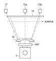
また、シリンドリカルレンズ6とポリゴンミラー2との間の光路中に配置され、レーザダイオード1から出射された光束を電圧印加により副走査方向に偏向する電気光学結晶構造体12を備える。ここで、副走査方向とは、電気光学結晶構造体12内を通過する光束の進路方向に対して垂直方向であり、図1Bの示す副走査方向に相当する。また、前記副走査方向に偏向された光束を検知するビームディテクトセンサ(以下、BDセンサという)17及び光検知センサ75a,75bと、ポリゴンミラー2によって走査された光束を反射部材18を介して感光ドラム8上に結像するfθレンズ14とを備える。BDセンサ17及び光検知センサ75a、75bの各光路の上流には、各センサ面で光束を集光させるための集光レンズ76がそれぞれ配置されている。
The electro-
また、光走査装置90は、電気光学結晶構造体12に電気的に接続され、電気光学結晶構造体12に印加する電圧を制御する電圧制御部19を備える。また、LD駆動制御部82は、BDセンサ17及び光検知センサ75a,75bの検知結果に基づいて、レーザダイオード1から出射される光束の感光ドラム15上における照射位置を制御する走査制御部60からの出力信号により制御される。
The
尚、BDセンサ17は、感光ドラム15の主走査方向の書き込み基準となる水平同期信号(BD信号)も検出する。
The
(電気光学結晶構造体12の構成例)
図2は、図1における電気光学結晶構造体12の構成を概略的に示す斜視図である。
(Configuration example of electro-optic crystal structure 12)
FIG. 2 is a perspective view schematically showing the configuration of the electro-
図2に示すように、電気光学結晶構造体12は、光束の入射面201aおよび出射面201bを有する直方体形状の電気光学結晶(以下、「EO結晶」という)41を備える。また、副走査方向に対して直角をなす両端面に取り付けられた一対の電極部に相当する電極74a,74bと、一対の電極74a,74b間に電圧を印加する不図示の電源とを備える。電極74a,74bは比較的細い電極幅d、長さLにて直線短冊形状に形成されたものである。電極74a,74bの材料は例えばAuが使用されるが、他の導電性材料であってもよい。製法は真空蒸着法による。
As shown in FIG. 2, the electro-
一対の電極74a,74bは、EO結晶41の内部に、EO結晶41内を通過する光束の進路に対して垂直方向(図2の副走査方向、図1Bの上下方向)の電界を形成する。
The pair of
電極74a,74bに電圧を印加しない状態では、EO結晶41はレンズ作用を持たず、入射面201aに入射された入射ビームは偏向されず、そのまま出射面201bからポリゴンミラー5へ向けて出射される。
In a state where no voltage is applied to the
一対の電極74a,74bに最大2〜5kVの電圧を印加して電気光学結晶41内に電界を発生させることにより電界分布が生じ、ms〜ns単位の時間内に光束を副走査方向に数度、例えば3度偏向する。電気光学結晶構造体12は、この高速かつ広角な電気光学効果により、非画像形成時に光束をポリゴンミラー5を介して、反射部材18から副走査方向に離れて配置されたBDセンサ17及び光検知センサ75a,75bに導く。
By applying a voltage of 2 to 5 kV at the maximum to the pair of
ここで、電気光学結晶とは、電圧を印加することにより屈折率が変化する特性を有する結晶である。EO結晶21は、カリウム,タンタル,ニオブおよび酸素から成る電気光学結晶で形成されている。例えば、KTN(KTaNbO3 :タンタル酸ニオブ酸カリウム、KTa1-xNbxO3)結晶等の電気光学結晶である。KTN結晶は、通常の光学ガラス同様に扱うことが可能であり、良好な加工性を有して切削や研磨加工での表面精度の確保が容易である。また、KTN結晶の光線の透過率については、レーザの波長である赤外から可視光全域に至るまで1mあたり95%以上の内部透過率を示し、複屈折も小さい。さらに、KTN結晶の吸水率は、通常のガラス以下であって、樹脂などに対して極端に小さい。
Here, the electro-optic crystal is a crystal having a characteristic that the refractive index changes when a voltage is applied. The
また、KTN結晶は、内部に電界を作用させることで内部の屈折率が変化することが知られている。KTN結晶の両端に電極を設置(一方に電圧=V、他方に電圧=0)して内部に電界を発生させた場合には、内部に電界が傾斜して分布することにより屈折率もその影響で傾斜して分布することになり、光が方向を変えながら進むことが判っている。KTN結晶は、高速かつ広角走査が可能という特徴がある。 In addition, it is known that the internal refractive index of a KTN crystal changes when an electric field is applied to the inside. When electrodes are installed at both ends of the KTN crystal (voltage = V on one side and voltage = 0 on the other) and an electric field is generated inside, the refractive index is also affected by the distribution of the electric field inside It is known that the light travels while changing its direction. The KTN crystal is characterized by being capable of high-speed and wide-angle scanning.
EO結晶41は、その両端部に印加する電圧の増大に応じて、EO結晶41内を通過する光束の進路がその電界方向(本例では副走査方向)に、大きく偏向される。本発明では、この現象を利用してレーザビームを透過させる際に進路を変化させるものである。
As the voltage applied to both ends of the
(電圧制御部19の構成例)
電圧制御部19は、制御電源70、制御電源70の駆動を制御する電源駆動制御部71、及び電気光学結晶構造体12に印加される電圧を切り替えるスイッチング手段72を備える。そして、電気光学結晶構造体12に電圧を選択的に印加し得るように構成されている。尚、本例における電気光学結晶構造体12による偏向角度は3度としているが、BDセンサ17及び光検知センサ75a,75bが配置される位置に応じて適切な値に変更される。
(Configuration example of voltage control unit 19)
The
(各センサの配置例)
BDセンサ17及び光検知センサ75a,75bは、感光ドラム15に走査される光束の最初の照射位置(ドット位置)、中心照射位置及び最後の照射位置に設けられる。すなわち、感光ドラム15上に形成される静電潜像に対応する画像形成領域内の中心部及び両端部に相当する。また、BDセンサ17及び光検知センサ75a,75bは、光検知センサ75aを中心として感光ドラムの長手方向(軸方向)、すなわち反射部材18の長手方向である主走査方向に関して等間隔に配置されている。これにより、fθレンズ14の収差等の影響による画像形成位置を補正するための、走査する光束の検知精度の悪化を抑制することができる。
(Example of arrangement of each sensor)
The
(走査制御部60の構成例)
走査制御部60は、BDセンサ17及び光検知センサ75a,75bの各検知信号に基づいて、画像形成領域の中心部及び両端部のドット位置のずれを検出するドット位置ずれ検出部80を備える。また、ドット位置ずれ検出部80により検出されたドット位置のずれを補正するように、画像データ処理を実行してレーザダイオード1の発光タイミングを制御する信号を出力する変調/画像データ処理部81とを備える。変調/画像データ処理部81は、レーザダイオード1の発光タイミングを制御する信号をLD駆動制御部82に出力する。
(Configuration Example of Scanning Control Unit 60)
The
<本光走査装置の動作例>
レーザダイオード1から発光されたレーザ光は、コリメータレンズ13を介して略平行光束へ変換される。その後、略平行光束はシリンドリカルレンズ6を通過して副走査方向集光される。シリンドリカルレンズ6を通過した光束は、電気光学結晶構造体12を透過し、ポリゴンモータ3によって回転駆動されるポリゴンミラー2に照射される。
<Operation example of this optical scanning device>
Laser light emitted from the
ポリゴンミラー2に照射された光束は、偏向走査されてfθレンズ14へ導かれる。画像形成時間内では、電気光学結晶構造体12による偏向が無いので、このfθレンズ14を通過した光束は、反射部材18で反射されて感光ドラム15上に結像し、主走査方向を等速で走査する。この光束の走査、すなわちスキャン動作により、感光ドラム15上に静電潜像が形成される。
The light beam applied to the
一方、画像形成時間外の所定のタイミングでEO結晶41に電圧を印加するとEO結晶41内で副走査方向に2〜3度偏向されるので、ポリゴンミラー2により偏向される光束はBDセンサ17及び光検知センサ75a,75bへと導かれる。BDセンサ17及び光検知センサ75a,75bは、ポリゴンミラー2により走査される光束の通過タイミングを検知する。尚、画像形成装置100において複数枚単位の画像処理が実行される場合は、次のような動作をする。すなわち、電気光学結晶構造体12は、1単位の画像に対応する静電潜像形成の終了時から次の1単位の画像に対応する静電潜像形成の開始時までの間に、レーザダイオード1から出射された光束を副走査方向に偏向する。これにより、画像を連続して出力する場合においても主走査方向のドット位置のずれの補正を適宜行うことができ、位置精度の高い静電潜像を形成することが可能となる。
On the other hand, when a voltage is applied to the
BDセンサ17は、反射部材18の上方且つ反射部材18の走査開始側の端部近傍に配置されている。BDセンサ17は、電気光学結晶構造体12により副走査方向に偏向され、且つポリゴンミラー2により主走査方向に偏向走査された光束を検知する。具体的には、レーザダイオード1が感光ドラム15に照射される光束のスキャン開始に当たる時間に強制点灯されると、BDセンサ17は、レーザダイオード1の強制点灯期間にポリゴンミラー2により偏向走査された光束を検知する。そして、主走査毎の画像形成における書き込み開始タイミングの基準信号となるビームディテクト信号(以下、BD信号という)を、後述するドット位置ずれ検出部80に出力する。
The
光検知センサ75aは、反射部材18の上方且つ反射部材18のほぼ中央部に配置され、光検知センサ75bは、反射部材18の上方且つ反射部材18の走査終了側の端部近傍に配置されている。光検知センサ75a、75bは、電気光学結晶構造体12により副走査方向に偏向され、且つポリゴンミラー2により主走査方向に偏向走査された光束を検知する。具体的には、光検知センサ75a,75bは、レーザダイオード1の強制点灯期間にポリゴンミラー2により偏向走査された光束を検知する。そして、主走査毎の画像形成における書き込み中間タイミングに応じた信号(以下、単に「中間タイミング信号」という)及び書き込み終了タイミングに応じた信号(以下、単に「終了タイミング信号」という)を夫々、ドット位置ずれ検出部80に出力する。
The
BDセンサ17及び光検知センサ75a,75bから出力されたBD信号、中間タイミング信号及び終了タイミング信号は、夫々、ドット位置ずれ検出部80でずれ量を求め、変調/画像データ処理部81へと入力される。そして、変調/画像データ処理部81により画像データの主走査方向のドット位置ずれが補正される。具体的には、BD信号、中間タイミング信号及び終了タイミング信号に基づいて、画像データの最初のドット位置から中心ドット位置までの距離の理論距離からのずれ量(以下、第1のずれ量という)が算出される。また、画像データの中心ドット位置から最後のドット位置までの距離の理論距離からのずれ量(以下、第2のずれ量という)が算出される。そして、算出された第1のずれ量と第2のずれ量とを比較する。上記第1のずれ量と第2のずれ量との差が0又は最小となるように、画像データの最初のドット位置及び最後のドット位置を変更する。その後、補正されたドット位置変更に基づいてレーザダイオード1の発光タイミングを示す信号をLD駆動制御部82に出力して、LD駆動制御部82を制御し、レーザダイオード1の発光タイミングを変更する。これにより、感光ドラム15上に形成される静電潜像に対応する画像形成領域内での、理論ドット位置からの主走査方向のずれが補正される。
The BD signal, the intermediate timing signal, and the end timing signal output from the
(走査制御部60の構成例)
図3は、図1における走査制御部60の内部構成を示すブロック図である。
(Configuration Example of Scanning Control Unit 60)
FIG. 3 is a block diagram showing an internal configuration of the
走査制御部60は、画像クロックを変調することによって、主走査ラインの印字位置のずれを補正することが可能な回路である。走査制御部60は、図3に示すように、ドット位置ずれ検出部80と変調/画像データ処理部81とを備える。
The
ドット位置ずれ検出部80は、主走査間隔dk検出回路1を備える。主走査間隔dk検出回路1は、BDセンサ17及び光検知センサ75a,75bから出力されたBD信号、中間タイミング信号及び終了タイミング信号から各センサ間距離を主走査間隔として検出する。そして、検出された間隔の値を示す主走査間隔信号2を出力する。この主走査間隔信号2は、主走査間隔dk計測回路3に入力され、主走査間隔dk計測回路3は、主走査間隔信号2を、時間データである主走査間隔計測信号4に変換する。主走査間隔計測信号4は、誤差比率γk算出回路13に供給される。
The dot position
誤差比率γk算出回路13は、主走査間隔計測信号4が示す値と予めfθレンズ14の特性に基づいて求め、所定値d格納回路11に予め設定されている所定値12との比率を算出し、その比率を誤差比率信号14として出力する。この誤差比率信号14は、誤差比率γk格納回路15に格納される。この誤差比率γkがずれ量に関する値となる。
The error ratio
誤差比率γk格納回路15に格納された誤差比率信号14は、変調/画像データ処理部81に入力される。変調/画像データ処理部81は、誤差比率信号14が示す値に基づいて予め設定された画像クロックを周波数変調し、画像クロック18として出力する。
The
次に、上記変調/画像データ処理部81の構成について説明する。変調/画像データ処理部81は、図3に示すように、基準クロック発生部20と、変倍係数設定レジスタ22と、補助画素発生回路24と、初期周期設定レジスタ26と、変調クロック制御回路30と変調クロック発生回路28とを有する。
Next, the configuration of the modulation / image
基準クロック発生部20は、任意の周波数である基準クロック信号21を発生する。変倍係数設定レジスタ22においては、誤差比率γk(および以下のセグメント数)に応じて、基準クロック信号21の周期比率を可変するための変倍係数(αk)23が設定され、保持される。
The
補助画素発生回路24は、基準クロック信号21および変倍係数23に基づいて補助画素周期25を発生する。この補助画素周期25により、主走査方向の倍率が補正される。すなわち、図1のポリゴンミラー2とfθレンズ14の光学系や環境変化などに起因して、感光ドラム15上に形成される主走査方向のドットの幅又はドット間隔が均一ではなくなる。そのため、補助画素周期25を用いて、ドット幅またはドット間隔が均一になるように1走査区間中における画像クロック18の周波数の補正が行われる。
The auxiliary
(ポリゴンミラーの回転によるずれ補正例)
ポリゴンミラー2のような回転走査系の場合、感光ドラム15の主走査方向における両端部は走査スピードが速くなる傾向があり、逆に、感光ドラム15の主走査方向における中央部は走査速度が遅くなる傾向にある。従って、感光ドラム15の両端部近傍の画像クロック18の周波数を速くし、感光ドラム15の中央部の画像クロック18の周波数を遅くするよう補正することにより、感光ドラム15上のドット幅またはドット間隔を均一にすることが可能になる。
(Example of displacement correction by rotation of polygon mirror)
In the case of a rotational scanning system such as the
ここで、例えば基準クロック信号21の周期をτref、変倍係数23をαk、補助画素周期25をΔτとすると、Δτは次の(1)式で表される。
Here, for example, assuming that the period of the
Δτ=αk×τref …(1)
ここで、変倍係数23(αk)は、補助画素周期25(Δτ)が画像クロック18の周期より充分に短くなるような値に設定されている。
Δτ = αk × τref (1)
Here, the scaling coefficient 23 (αk) is set to a value such that the auxiliary pixel period 25 (Δτ) is sufficiently shorter than the period of the
初期周期設定レジスタ26においては、画像クロック生成部17から出力される画像クロック18の周期の初期値27(τvdo)が設定され、保持される。
In the initial
変調クロック制御回路30は、主走査方向に走査する1ライン内を、任意数の画素で構成するセグメントに分割し、複数のセグメントを形成すると共に、各セグメント内の画像クロック18の周期を一定にする。
The modulation
(変調クロック制御回路30の動作例)
図4は、図2における変調クロック制御回路30で形成されるセグメントの一部と各セグメント内の画像クロック18の周期との関係を示す図である。
(Operation Example of Modulation Clock Control Circuit 30)
FIG. 4 is a diagram showing a relationship between a part of the segments formed by the modulation
図4において、変調クロック制御回路30は、BDセンサ17から出力される書き出し基準となる信号であるBD信号29が入力される。すると、変調クロック制御回路30は、最初のセグメント(セグメント0)に対する変調クロック制御信号33を生成し、変調クロック発生回路28に出力する。この変調クロック制御信号33を受けた変調クロック発生回路28は、初期周期設定レジスタ26に保持されている初期周期27(τvdo)の画像クロック18を出力する。また、次のセグメント(セグメント1)に対しては、変調クロック制御回路30は、次のセグメント(セグメント1)に対する変調クロック制御信号33を生成し、変調クロック発生回路28に出力する。この変調クロック制御信号33を受けた変調クロック発生回路28は、初期周期27(=τvdo)と補助画素周期25(=Δτ)とに基づいて、下記(2)式で表される周期を有する変調クロックτ1を生成する。そして、該変調クロックτ1を画像クロック18として出力する。
In FIG. 4, the modulation
τ1=τvdo+Δτ
=τvdo+(α1×τref) …(2)
ここで、α1はセグメント1に対する変倍係数である。
τ1 = τvdo + Δτ
= Τvdo + (α1 × τref) (2)
Here, α1 is a scaling factor for
同様に、さらに次のセグメント(セグメント2)に対しては、変調クロック制御回路30は、さらに次のセグメント(セグメント2)に対する変調クロック制御信号33を変調クロック発生回路28に出力する。
Similarly, for a further next segment (segment 2), the modulation
この変調クロック制御信号を受けた変調クロック発生回路28は、初期周期27(=τvdo)と補助画素周期25とを用いて、下記(3)式で表される周期を有する変調クロックτ2を生成する。そして、該変調クロックτ2を画像クロック18として出力する。
Upon receiving this modulation clock control signal, the modulation clock generation circuit 28 uses the initial period 27 (= τvdo) and the
τ2=τvdo+(α1×τref)+(α2×τref) …(3)
ここで、α2はセグメント2に対する変倍係数である。
τ2 = τvdo + (α1 × τref) + (α2 × τref) (3)
Here, α2 is a scaling factor for
また、セグメント2以降の他のセグメントに対しても、上記同様の手順でそのセグメントに対する変調クロックτnが生成され、該変調クロックτnが画像クロック18として出力される。
Further, the modulation clock τn for the other segments after the
以上のように、変調クロック制御回路30により、1主走査ライン内において各セグメントに対応する複数の画像クロック18が変調クロック発生回路28から出力される。
As described above, the modulation
(1セグメント内の多段階可変の例)
図5A及び図5Bは、1セグメント内の画像クロック18を多段階に可変させた場合における、セグメントと該セグメント内の画像クロック18の周期との関係を示す図である。図5Aは、初期セグメントが可変である場合を示し、図5Bは、初期セグメントが固定である場合を示す。以下に、図5A及び図5Bを用いて、1つのセグメント内で周波数変調を行った場合についてのセグメント周期の制御方法を説明する。
(Example of multi-stage variable within one segment)
5A and 5B are diagrams showing the relationship between the segment and the period of the
(1)初期セグメント(セグメント0)可変の場合
初期周期をτvdo、1セグメント当りの画素数をn、変倍係数(セグメント1)をα1、及び基準クロック周期をτrefとする。この場合、Δτa(セグメント0での1画素当りの周期)及びΔT0(セグメント0の総周期)は、下記(4)式及び(5)式で表される。
(1) When Initial Segment (Segment 0) is Variable Assume that the initial period is τvdo, the number of pixels per segment is n, the scaling factor (segment 1) is α1, and the reference clock period is τref. In this case, Δτa (period per pixel in segment 0) and ΔT0 (total period of segment 0) are expressed by the following equations (4) and (5).
Δτa=(α1×τref)/n ……(4)
ΔT0=τvdo+{n×(n+1)/2}×{(α1×τref)/n}
=τvdo+(n+1)/2×(α1×τref) ……(5)
(2)初期セグメント(セグメント0)固定の場合
初期周期をτvdoとすると、セグメント0の総周期ΔT0は、下記(6)式で表される。
Δτa = (α1 × τref) / n (4)
ΔT0 = τvdo + {n × (n + 1) / 2} × {(α1 × τref) / n}
= Τvdo + (n + 1) / 2 × (α1 × τref) (5)
(2) When Initial Segment (Segment 0) is Fixed Assuming that the initial period is τvdo, the total period ΔT0 of segment 0 is expressed by the following equation (6).
ΔT0=n×τvdo
一方、変倍係数(セグメント2)をα2、及び基準クロック周期をτrefとすると、Δτb(セグメント1での1画素当りの周期)及びΔT1(セグメント1の総周期)は、下記(6)式及び(7)式で表される。
ΔT0 = n × τvdo
On the other hand, when the scaling factor (segment 2) is α2 and the reference clock period is τref, Δτb (period per pixel in segment 1) and ΔT1 (total period of segment 1) are expressed by the following equation (6): It is represented by the formula (7).
Δτb=(α2×τref)/n ……(6)
ΔT1=τvdo+{n×(n+1)/2}×{(α2×τref)/n}
=τvdo+(n+1)/2×(α2×τref) ……(7)
そして、さらにセグメント1以降の各セグメントに関しては、同様の式で1画素当りの周期△τb及び各セグメントの総周期△Tn(n≧2)を表すことができる。
Δτb = (α2 × τref) / n (6)
ΔT1 = τvdo + {n × (n + 1) / 2} × {(α2 × τref) / n}
= Τvdo + (n + 1) / 2 × (α2 × τref) (7)
Further, for each segment after
画像データ107と上記で算出した画像クロック18は、PWM(Pulse Width Modulation)発生部105へと入力される。PWM発生部105は、算出した画像クロック18と画像データ107とに応じて、1クロック内のレーザのON/OFF時間を制御するパルスを生成してレーザ駆動制御部82に出力して、レーザダイオード1からの光束の出射を制御する。
The image data 107 and the
<光走査装置の主走査方向の倍率制御処理の手順例>
図6は、図1における光走査装置90で実行される主走査方向の倍率制御処理を示すフローチャートである。
<Procedure example of magnification control processing in main scanning direction of optical scanning device>
FIG. 6 is a flowchart showing magnification control processing in the main scanning direction, which is executed by the
図6において、まず、画像形成時間外の所定のタイミングで主走査方向の倍率の制御開始要求を受けると、EO結晶41に取り付けられた一対の電極74a,74bに電圧が印可される(ステップS600)。また、ほぼ同時に、レーザ点灯、ポリゴンモータ3の回転動作が行われ、走査光はEO結晶41により副走査方向に偏向され、BDセンサ17及び光検知センサ75a,75bへ向かう位置に導かれる。これにより、走査光の3点同期計測が行われ、BDセンサ17及び光検知センサ75a,75bから送信される各タイミング信号に基づいて走査光のカウント値が読取られる(ステップS601)。
In FIG. 6, when a request for starting magnification control in the main scanning direction is received at a predetermined timing outside the image formation time, a voltage is applied to the pair of
その後、ステップS601にて読取られたカウント値を理想タイミングからの主走査方向の倍率誤差に変換し(ステップS602)、該主走査方向の倍率誤差が許容範囲(Ethで示す)内か否かを判定する(ステップS603)。主走査方向の倍率誤差が許容範囲内(≦Eth)であるときは本処理を終了し、画像形成装置は画像形成動作待ち状態になる。 Thereafter, the count value read in step S601 is converted into a magnification error in the main scanning direction from the ideal timing (step S602), and whether or not the magnification error in the main scanning direction is within an allowable range (shown as Eth). Determination is made (step S603). When the magnification error in the main scanning direction is within the allowable range (≦ Eth), this process is terminated, and the image forming apparatus enters an image forming operation waiting state.
一方、主走査倍率誤差が許容範囲外(>Eth)であるとき、すなわちドット位置ずれが発生している場合は、ポリゴンロック信号の検出等によりポリゴンミラー2が正常に作動しているか否かを判定する(ステップS604)。ポリゴンミラー2の作動が異常であるときは、サービスマンコール等を操作部に表示するエラー表示を行う(ステップS605)。
On the other hand, when the main scanning magnification error is outside the allowable range (> Eth), that is, when a dot position shift has occurred, it is determined whether or not the
ポリゴンミラー2の作動が正常である場合は、変調/画像データ処理部81により変調/画像データ処理を行い(ステップS606)、補正された画像クロックに基づく画像データ信号を出力し(ステップ6907)、画像形成待機状態となり、本処理を終了する。
When the operation of the
(第1の実施形態の効果)
本実施の形態によれば、電気光学結晶構造体12が、シリンドリカルレンズ6とポリゴンミラー2との間の光路中に配置されると共に、レーザダイオード1から出射された光束を電圧印加により副走査方向に偏向する。また、BDセンサ17及び光検知センサ75a,75bが、感光ドラム15上に形成される静電潜像に対応する画像形成領域の中央部及び両端部に設けられる。そして、走査制御部60が、BDセンサ17及び光検知センサ75a,75bの検知結果に基づいて、感光ドラム15上における光束の主走査方向の照射位置を制御する。従って、途中で光束を分岐させることなく光束のずれを検知することができるので、光量の損失の影響を受けない高精度な光束検知を実行できる。同時に、画像形成領域内でのドット位置ずれを正確に補正することができ、もって検知精度を向上しつつ画像形成位置を正確に補正することができる。
(Effects of the first embodiment)
According to the present embodiment, the electro-
また、従来のようにハーフミラーなどによって、光源から出射された光束を分離するのではなく、全光束を用いて光束のずれを検知することができる。そのため、VCSEL等の最大出力が小さい光源を用いた場合であっても、高精度な光束検知を実行できる。 In addition, the light flux emitted from the light source is not separated by a half mirror as in the prior art, but the deviation of the light flux can be detected using the total light flux. Therefore, even when a light source having a small maximum output, such as a VCSEL, is used, highly accurate light flux detection can be executed.
また、電気光学結晶構造体12としてKTN結晶を使用することで、KTN結晶の光線の透過率がレーザの波長である赤外から可視光全域に至るまで1mあたり95%以上の内部透過率を示す。また、複屈折も小さいので、高精度な光束検知を行うことができる。
In addition, by using a KTN crystal as the electro-
さらに、ずれ検知を行う際、全光束がBDセンサ17及び光検知センサ75a,75bの方向に偏向されて入射しているため、光束分離方式のようにずれ検知の際の発光が感光ドラムを走査してしまう恐れがない。
Further, when detecting the deviation, since all the light beams are deflected and incident in the direction of the
また、主走査方向に関して画像形成領域から前後に大きくずれた位置(本例では、反射部材18の主走査方向の外側)に光検知センサを配置する必要がなく、装置の小型化も可能となる。
In addition, it is not necessary to arrange a light detection sensor at a position (in this example, outside of the reflecting
本実施の形態では、光検知センサ75a,75bは前述の位置に配置されるが、これに限るものではなく、偏向走査された光束を検知しうる画像形成領域近傍の範囲内であれば前述した位置以外の位置に配置されてもよい。また、光検知センサは、主走査方向に沿って等間隔に3つ以上設置されてもよい。これにより、さらに高精度な主走査倍率の補正が可能となる。
In the present embodiment, the
また、本実施の形態では、副走査方向に偏向された光束を検知する3つの検知センサ(BDセンサ17及び光検知センサ75a,75b)が配置されるが、これに限るものではない。副走査方向に偏向走査された光束を検知しうる画像領域内に3以上の光検知センサが配置されてもよい。光検知センサを増加することにより、検知精度を向上しつつ画像形成位置を正確に補正することができる。
In the present embodiment, three detection sensors (
<光走査装置の第2の構成例>
図7は、本発明の第2の実施形態に係る光走査装置の構成を概略的に示す平面図である。尚、本第2の実施形態は、その構成が上記第1の実施形態と同じであり、同じ構成要素については、同一の符号を付して重複した説明を省略し、以下に異なる部分を説明する。
<Second Configuration Example of Optical Scanning Device>
FIG. 7 is a plan view schematically showing the configuration of the optical scanning device according to the second embodiment of the present invention. The configuration of the second embodiment is the same as that of the first embodiment, and the same components are denoted by the same reference numerals and redundant description is omitted, and different portions are described below. To do.
図7において、光走査装置700は、電気光学結晶構造体12により副走査方向に偏向された光束を所定方向に反射する光検知用反射部材717を備える。また、光検知用反射部材717により反射された光束を検知するBDセンサ717及び光検知センサ775a,775bとを備える。BDセンサ717は、ポリゴンミラー2での光束の偏向点からBDセンサ717の受光面までの光路長さが、ポリゴンミラー2での光束の偏向点から感光ドラム15の表面までの光路長さと略同一となる位置に配置される。光検知センサ775a,775bも、ポリゴンミラー2での光束の偏向点から光検知センサ775a,775bの受光面までの光路長さが、ポリゴンミラー2での光束の偏向点から感光ドラム15の表面までの光路長さと略同一となる位置に配置される。これにより、感光ドラム15の表面でのドット位置ずれをより精度良く検知することができ、主走査方向の画像データの補正精度を更に向上させることができる。
In FIG. 7, the
<光走査装置の第3の構成例>
図8は、本発明の第3の実施形態に係る光走査装置の構成を概略的に示す平面図である。尚、本第3の実施形態は、その構成が上記第1の実施形態と同じであり、同じ構成要素については、同一の符号を付して重複した説明を省略し、以下に異なる部分を説明する。
<Third Configuration Example of Optical Scanning Device>
FIG. 8 is a plan view schematically showing the configuration of the optical scanning device according to the third embodiment of the present invention. The configuration of the third embodiment is the same as that of the first embodiment, and the same components are denoted by the same reference numerals and redundant description is omitted, and different portions are described below. To do.
図8において、光走査装置800は、副走査方向に関してポリゴンミラー2と略同一面内に配置されたBDセンサ801を備える。また、反射部材18の上方に配置され且つ反射部材18の、走査開始側端部近傍、ほぼ中央部及び走査終了側端部近傍に配置された光検知センサ802a,802b,802cを備える。具体的に、光検知センサ802aは、感光ドラム15に走査される光束の最初の照射位置(図中の位置A)より内側に配置され、光検知センサ802cは、感光ドラム15に走査される光束の最後の照射位置(図中の位置B)より内側に配置される。これにより、全ての光検知センサを主走査方向に関して反射部材18の両端より内側に配置することができ、装置の小型化が可能となる。
In FIG. 8, the optical scanning device 800 includes a BD sensor 801 disposed in substantially the same plane as the
<光走査装置の更に他の構成例>
上記実施形態では、電気光学結晶構造体12は、シリンドリカルレンズ6とポリゴンミラー2との間の光路中に配置されるが、これに限るものではない。
<Another configuration example of the optical scanning device>
In the above embodiment, the electro-
図9に示すように、ポリゴンミラー2とfθレンズ14の間の光路中に配置されてもよい。この場合、電気光学結晶構造体900は、主走査方向に延びる略長尺状のEO結晶を有し、ポリゴンミラー2により主走査方向に走査する光束を偏向する。また、電気光学結晶構造体は、レーザダイオード1とポリゴンミラー2との間の光路中のいずれの位置に配置されてもよく、ポリゴンミラー2への入射側光路中又はポリゴンミラー2からの出射側光路中のいずれの位置に配置されてもよい。
As shown in FIG. 9, it may be disposed in the optical path between the
また、上記実施形態では、ポリゴンミラー2によって変更された光束が感光ドラム15を走査する。しかし、これに限るものではなく、ガルバノミラーやMEMS(Micro Electro Mechanical System)を使用して感光ドラムを走査する構成であってもよい。
In the above embodiment, the light beam changed by the
Claims (14)
前記光源から出射された光束を偏向して、偏向された光束で感光体を主走査方向に走査する光走査手段と、
前記光源と複数の光検知手段との間の光路に配置され、前記光源から出射された光束を電圧印加により副走査方向に偏向する電気光学結晶構造体と、
前記副走査方向に偏向された光束を検知する複数の前記光検知手段とを備え、
前記複数の光検知手段は、前記感光体に形成される静電潜像に対応する主走査方向の画像形成領域内に設けられ、前記複数の光検知手段の出力が、前記感光体上の光束の主走査方向の照射位置を制御するために使用されることを特徴とする光走査装置。 A light source that emits a luminous flux;
An optical scanning means for deflecting a light beam emitted from the light source and scanning the photosensitive member in the main scanning direction with the deflected light beam;
An electro-optic crystal structure that is disposed in an optical path between the light source and a plurality of light detection means, and deflects a light beam emitted from the light source in a sub-scanning direction by applying a voltage;
A plurality of the light detection means for detecting a light beam deflected in the sub-scanning direction,
The plurality of light detection means are provided in an image forming area in a main scanning direction corresponding to an electrostatic latent image formed on the photoconductor, and an output of the plurality of light detection means is a light flux on the photoconductor An optical scanning device used for controlling the irradiation position in the main scanning direction.
前記電気光学結晶に印加される電圧を制御する電圧制御手段を更に備えることを特徴とする請求項1に記載の光走査装置。 The electro-optic crystal structure is an electro-optic crystal having a characteristic that a refractive index changes when a voltage is applied,
The optical scanning device according to claim 1, further comprising voltage control means for controlling a voltage applied to the electro-optic crystal.
前記一対の電極部は、前記電気光学結晶の内部に、前記電気光学結晶を通過する光束の進路方向に対して直角に副走査方向の電界を形成することを特徴とする請求項5に記載の光走査装置。 The voltage control means has a pair of electrode parts attached to the electro-optic crystal,
6. The pair of electrode portions form an electric field in a sub-scanning direction perpendicular to a traveling direction of a light beam passing through the electro-optic crystal inside the electro-optic crystal. Optical scanning device.
前記光走査装置が、
光束を出射する光源と、
前記光源から出射された光束を偏向して、偏向された光束で感光体を主走査方向に走査する光走査手段と、
前記光源と複数の光検知手段との間の光路に配置され、前記光源から出射された光束を電圧印加により副走査方向に偏向する電気光学結晶構造体と、
前記副走査方向に偏向された光束を検知する複数の前記光検知手段とを備え、
前記複数の光検知手段は、前記感光体に形成される静電潜像に対応する主走査方向の画像形成領域内に設けられ、前記複数の光検知手段の出力が、前記感光体上の光束の主走査方向の照射位置を制御するために使用されることを特徴とする画像形成装置。 An image forming apparatus having an optical scanning device,
The optical scanning device is
A light source that emits a luminous flux;
An optical scanning means for deflecting a light beam emitted from the light source and scanning the photosensitive member in the main scanning direction with the deflected light beam;
An electro-optic crystal structure that is disposed in an optical path between the light source and a plurality of light detection means, and deflects a light beam emitted from the light source in a sub-scanning direction by applying a voltage;
A plurality of the light detection means for detecting a light beam deflected in the sub-scanning direction,
The plurality of light detection means are provided in an image forming area in a main scanning direction corresponding to an electrostatic latent image formed on the photoconductor, and an output of the plurality of light detection means is a light flux on the photoconductor An image forming apparatus used for controlling the irradiation position in the main scanning direction.
前記電気光学結晶に印加される電圧を制御する電圧制御手段を更に備えることを特徴とする請求項10に記載の画像形成装置。 The electro-optic crystal structure is an electro-optic crystal having a characteristic that a refractive index changes when a voltage is applied,
The image forming apparatus according to claim 10, further comprising a voltage control unit that controls a voltage applied to the electro-optic crystal.
前記光束のON/OFF時間を制御する信号に対応して、前記光源から出射される光束の駆動を制御する光束駆動制御手段とを更に備えることを特徴とする請求項10に記載の画像形成装置。 Scanning control means for controlling the irradiation position of the light flux on the photosensitive member in the main scanning direction by generating a signal for controlling the ON / OFF time of the light flux based on the detection results of the plurality of light detection means;
The image forming apparatus according to claim 10, further comprising: a light beam driving control unit that controls driving of the light beam emitted from the light source in response to a signal for controlling an ON / OFF time of the light beam. .
Priority Applications (2)
| Application Number | Priority Date | Filing Date | Title |
|---|---|---|---|
| JP2007324019A JP2008181104A (en) | 2006-12-28 | 2007-12-14 | Optical scanning device and image forming device equipped with the optical scanning device |
| US11/959,954 US7782511B2 (en) | 2006-12-28 | 2007-12-19 | Optical scanning apparatus and image forming apparatus comprising the same |
Applications Claiming Priority (2)
| Application Number | Priority Date | Filing Date | Title |
|---|---|---|---|
| JP2006355160 | 2006-12-28 | ||
| JP2007324019A JP2008181104A (en) | 2006-12-28 | 2007-12-14 | Optical scanning device and image forming device equipped with the optical scanning device |
Publications (2)
| Publication Number | Publication Date |
|---|---|
| JP2008181104A true JP2008181104A (en) | 2008-08-07 |
| JP2008181104A5 JP2008181104A5 (en) | 2011-02-03 |
Family
ID=39725019
Family Applications (1)
| Application Number | Title | Priority Date | Filing Date |
|---|---|---|---|
| JP2007324019A Pending JP2008181104A (en) | 2006-12-28 | 2007-12-14 | Optical scanning device and image forming device equipped with the optical scanning device |
Country Status (1)
| Country | Link |
|---|---|
| JP (1) | JP2008181104A (en) |
Cited By (4)
| Publication number | Priority date | Publication date | Assignee | Title |
|---|---|---|---|---|
| JP2008245848A (en) * | 2007-03-29 | 2008-10-16 | Heiwa Corp | Game machine |
| JP2011027864A (en) * | 2009-07-23 | 2011-02-10 | Canon Inc | Optical apparatus |
| JP2012053438A (en) * | 2010-05-20 | 2012-03-15 | Ricoh Co Ltd | Optical scanner and image forming device |
| JP2013064773A (en) * | 2011-09-15 | 2013-04-11 | Ricoh Co Ltd | Optical deflector, optical scanner, and image forming device |
Citations (5)
| Publication number | Priority date | Publication date | Assignee | Title |
|---|---|---|---|---|
| JPS58134574A (en) * | 1982-02-03 | 1983-08-10 | インタ−ナショナル ビジネス マシ−ンズ コ−ポレ−ション | Feedback device in deflecting system |
| JPH04328777A (en) * | 1991-04-30 | 1992-11-17 | Fuji Xerox Co Ltd | Color image forming device |
| JPH11352862A (en) * | 1998-06-10 | 1999-12-24 | Nippon Telegr & Teleph Corp <Ntt> | Formation of hologram recording material |
| JP2003098458A (en) * | 2001-09-21 | 2003-04-03 | Ricoh Co Ltd | Optical scanner and its adjusting method |
| JP2003279873A (en) * | 2002-03-20 | 2003-10-02 | Ricoh Co Ltd | Optical scanner and image formation device |
-
2007
- 2007-12-14 JP JP2007324019A patent/JP2008181104A/en active Pending
Patent Citations (5)
| Publication number | Priority date | Publication date | Assignee | Title |
|---|---|---|---|---|
| JPS58134574A (en) * | 1982-02-03 | 1983-08-10 | インタ−ナショナル ビジネス マシ−ンズ コ−ポレ−ション | Feedback device in deflecting system |
| JPH04328777A (en) * | 1991-04-30 | 1992-11-17 | Fuji Xerox Co Ltd | Color image forming device |
| JPH11352862A (en) * | 1998-06-10 | 1999-12-24 | Nippon Telegr & Teleph Corp <Ntt> | Formation of hologram recording material |
| JP2003098458A (en) * | 2001-09-21 | 2003-04-03 | Ricoh Co Ltd | Optical scanner and its adjusting method |
| JP2003279873A (en) * | 2002-03-20 | 2003-10-02 | Ricoh Co Ltd | Optical scanner and image formation device |
Non-Patent Citations (1)
| Title |
|---|
| JPN7012004569; 日本電信電話(株): 'News Release 「光が自在に曲がる新現象を発見」' 日本電信電話(株)のNews Release , 20060518, 日本電信電話(株) * |
Cited By (5)
| Publication number | Priority date | Publication date | Assignee | Title |
|---|---|---|---|---|
| JP2008245848A (en) * | 2007-03-29 | 2008-10-16 | Heiwa Corp | Game machine |
| JP2011027864A (en) * | 2009-07-23 | 2011-02-10 | Canon Inc | Optical apparatus |
| JP2012053438A (en) * | 2010-05-20 | 2012-03-15 | Ricoh Co Ltd | Optical scanner and image forming device |
| US8179580B2 (en) | 2010-05-20 | 2012-05-15 | Ricoh Company, Ltd. | Optical scanning device and image forming apparatus |
| JP2013064773A (en) * | 2011-09-15 | 2013-04-11 | Ricoh Co Ltd | Optical deflector, optical scanner, and image forming device |
Similar Documents
| Publication | Publication Date | Title |
|---|---|---|
| US8005321B2 (en) | Pixel clock generator, optical scanner, and image forming apparatus | |
| JP5009573B2 (en) | Optical scanning apparatus and image forming apparatus | |
| JP5030517B2 (en) | Optical scanning apparatus, image forming apparatus, and color image forming apparatus | |
| JP2006175754A (en) | Image forming apparatus and image forming method | |
| JP2009244843A (en) | Optical scanning device and color image forming apparatus | |
| JP4980678B2 (en) | Optical scanning device, optical scanning device manufacturing method, and color image forming apparatus | |
| JP4428953B2 (en) | Optical scanning apparatus and color image forming apparatus | |
| JP5729545B2 (en) | Optical scanning apparatus and image forming apparatus | |
| JP2013140294A (en) | Optical scanner and image forming apparatus | |
| US7782511B2 (en) | Optical scanning apparatus and image forming apparatus comprising the same | |
| US7995088B2 (en) | Optical scanning apparatus and image forming apparatus comprising the same | |
| JP2008181104A (en) | Optical scanning device and image forming device equipped with the optical scanning device | |
| JP2002096502A (en) | Imaging apparatus | |
| US20080158633A1 (en) | Optical scanning apparatus | |
| JP4438300B2 (en) | Optical scanning apparatus, image forming apparatus, and image forming system | |
| KR20100077717A (en) | Light scanning unit caparable of compensating for zigzag error, image forming apparatus employing the same, and method of compensating for zigzag error of the light scanning unit | |
| JP2009222922A (en) | Laser scanner and image forming apparatus | |
| JP2007114518A (en) | Optical scanner, image forming apparatus, and method of correcting vertical scanning position | |
| US7460146B2 (en) | Dynamic correction of field curvature from a scanner | |
| JP2004045840A (en) | Method and device for optical scanning, and image forming device | |
| JP2008181103A (en) | Optical scanner, and image forming apparatus comprising the same | |
| JPH1155472A (en) | Multi-color image forming device | |
| JP5387455B2 (en) | Optical scanning device and image forming apparatus including the optical scanning device | |
| JP2009300833A (en) | Light scanning device and image forming apparatus equipped with the same | |
| JP4827504B2 (en) | Optical scanning device and image forming apparatus using the same |
Legal Events
| Date | Code | Title | Description |
|---|---|---|---|
| A521 | Written amendment |
Free format text: JAPANESE INTERMEDIATE CODE: A523 Effective date: 20101214 |
|
| A621 | Written request for application examination |
Free format text: JAPANESE INTERMEDIATE CODE: A621 Effective date: 20101214 |
|
| A977 | Report on retrieval |
Free format text: JAPANESE INTERMEDIATE CODE: A971007 Effective date: 20120112 |
|
| A131 | Notification of reasons for refusal |
Free format text: JAPANESE INTERMEDIATE CODE: A131 Effective date: 20120116 |
|
| A521 | Written amendment |
Free format text: JAPANESE INTERMEDIATE CODE: A523 Effective date: 20120306 |
|
| A131 | Notification of reasons for refusal |
Free format text: JAPANESE INTERMEDIATE CODE: A131 Effective date: 20121109 |
|
| A02 | Decision of refusal |
Free format text: JAPANESE INTERMEDIATE CODE: A02 Effective date: 20130329 |