JP2008172998A - High-voltage power supply unit, image forming device, and power supply controlling method - Google Patents
High-voltage power supply unit, image forming device, and power supply controlling method Download PDFInfo
- Publication number
- JP2008172998A JP2008172998A JP2007315005A JP2007315005A JP2008172998A JP 2008172998 A JP2008172998 A JP 2008172998A JP 2007315005 A JP2007315005 A JP 2007315005A JP 2007315005 A JP2007315005 A JP 2007315005A JP 2008172998 A JP2008172998 A JP 2008172998A
- Authority
- JP
- Japan
- Prior art keywords
- output
- power supply
- voltage power
- voltage
- outputs
- Prior art date
- Legal status (The legal status is an assumption and is not a legal conclusion. Google has not performed a legal analysis and makes no representation as to the accuracy of the status listed.)
- Pending
Links
Images


Abstract
Description
本発明は複数の出力を有する高圧電源装置、この高圧電源装置を備えた複写機、プリンタ、ファクシミリ及びこれらの装置の機能を備えたデジタル複合機等の画像形成装置、及び電源供給制御方法に関する。 The present invention relates to a high-voltage power supply apparatus having a plurality of outputs, a copier equipped with the high-voltage power supply apparatus, a printer, a facsimile, an image forming apparatus such as a digital multifunction peripheral equipped with the functions of these apparatuses, and a power supply control method.
電子複写機装置やレーザプリンタ装置等の画像形成装置においては、帯電装置、転写装置、現像装置等が内蔵されている。これらの装置を動作させる際には、高圧電源装置の出力が用いられている。画像形成装置の制御装置では、この高圧電源の出力電圧を調整しながら画像形成処理を行っている。また、複数色で構成されたカラー画像を形成するためのカラー画像形成装置においては、各色、すなわちC(シアン)M(マゼンタ)Y(イエロー)K(ブラック)のそれぞれの画像を形成するために、各色に対応した複数の帯電装置、転写装置、現像装置等が設けられている。 In an image forming apparatus such as an electronic copying machine or a laser printer, a charging device, a transfer device, a developing device, and the like are incorporated. When these devices are operated, the output of the high-voltage power supply device is used. In the control device of the image forming apparatus, image forming processing is performed while adjusting the output voltage of the high-voltage power supply. In a color image forming apparatus for forming a color image composed of a plurality of colors, in order to form each color, that is, an image of C (cyan), M (magenta), Y (yellow), and K (black). A plurality of charging devices, transfer devices, developing devices and the like corresponding to each color are provided.
安全上、高圧電源には異常時に高圧電源の出力を停止させる保護回路を設けていることが多いが、画像形成装置の高圧電源は複数の出力を有するので各出力に対しそれぞれ異常検知回路を設け保護動作を作動させる構成となっていた。 For safety reasons, the high-voltage power supply is often provided with a protection circuit that stops the output of the high-voltage power supply in the event of an abnormality. However, since the high-voltage power supply of the image forming apparatus has multiple outputs, an abnormality detection circuit is provided for each output. The configuration was such that the protective operation was activated.
この例として、例えば特許文献1又は2記載の発明が知られている。このうち特許文献1記載の発明は、出力電圧あるいは出力電流を所定値に制限する高圧電源装置の異常検出方式において、出力電力を検出する電力検出手段と、この電力検出手段の検出電力が所定の範囲を越えたことを検出する検出手段を備え、前記検出手段の出力により出力電圧あるいは出力電流を制限又は停止することを特徴としている。
As this example, for example, the invention described in
また、特許文献2記載の発明は、入力電圧を昇圧して負荷に供給する高圧電源装置において、負荷に以上電流が流れたときにそれを検出する異常電流検出手段と、が手段による異常電流の検出値に応じた時間だけ出力電流を低下させるように制御する出力電流制御手段と、該手段による出力電流を低下させる制御の繰り返しが連続して一定時間継続したときに高電圧出力動作を停止する手段と、を備えたことを特徴としている。
そのため多くの部品を使用しており、また基板サイズも出力数が増えるほど大きくなっていた。 For this reason, many parts are used, and the board size increases as the number of outputs increases.
そこで、本発明が解決すべき課題は、異常の検知と高圧電源すべての出力の停止を単一の異常検知回路で実行できるようにすることにある。 Therefore, a problem to be solved by the present invention is to enable detection of abnormality and stop of output of all high-voltage power supplies by a single abnormality detection circuit.
前記課題を解決するため、第1の手段は、異なる出力電圧を設定可能な複数の出力と、異常時に前記出力を停止させる単一の保護回路とを備え、前記保護回路は異常が発生したとき、前記複数の出力の全てを停止させる高圧電源装置を特徴とする。 In order to solve the above problem, the first means includes a plurality of outputs capable of setting different output voltages, and a single protection circuit that stops the output when an abnormality occurs, and the protection circuit has an abnormality. A high-voltage power supply device that stops all of the plurality of outputs is characterized.
第2の手段は、第1の手段において、前記複数の出力が第1の出力及び第2の出力の2出力であって、前記第1の出力及び第2の出力のそれぞれの異常を電圧によって検出する第1及び第2のエラー検出電圧発生部を備え、前記保護回路へは前記第1及び第2のエラー検出電圧発生部からの電圧が入力されることを特徴とする。 According to a second means, in the first means, the plurality of outputs are two outputs of a first output and a second output, and each abnormality of the first output and the second output is determined by a voltage. First and second error detection voltage generators for detection are provided, and voltages from the first and second error detection voltage generators are input to the protection circuit.
第3の手段は、第2の手段において、前記保護回路への前記第1及び第2のエラー検出電圧発生部からの電圧はツェナーダイオードを介して入力されることを特徴とする。 A third means is characterized in that, in the second means, the voltages from the first and second error detection voltage generation units to the protection circuit are inputted via a Zener diode.
第4の手段は、第1の手段において、前記保護回路内の異常検出部への入力部に、当該異常検出部側がアノード、信号の入力側がカソードとなるようにツェナーダイオードを設け、前記第1及び第2の出力のエラー検出電圧発生部を、ダイオードを通して1つにまとめ、前記ダイオードのカソード側を前記ツェナーダイオードのカソードと接続し、エラー検出電圧発生部の1つが予め設定された電圧以上になると前記異常検出部に信号が入力されることを特徴とする。 According to a fourth means, in the first means, a Zener diode is provided in an input part to the abnormality detection part in the protection circuit so that the abnormality detection part side is an anode and a signal input side is a cathode. And the second output error detection voltage generator is combined into one through a diode, the cathode side of the diode is connected to the cathode of the Zener diode, and one of the error detection voltage generators exceeds a preset voltage. Then, a signal is input to the abnormality detection unit.
第5の手段は、第1ないし第4のいずれかの手段において、前記保護回路は前記出力を停止させる際、出力電圧の値を制御する制御手段の電源を落とすことを特徴とする。 A fifth means is characterized in that, in any one of the first to fourth means, when the protection circuit stops the output, the control means for controlling the value of the output voltage is turned off.
第6の手段は、第1ないし第4のいずれかの手段において、前記保護回路は前記出力を停止させる際、高圧電源入力電圧を落とすことを特徴とする。 The sixth means is characterized in that, in any one of the first to fourth means, the protection circuit drops the high voltage power supply input voltage when stopping the output.
第7の手段は、第1ないし第6のいずれかの手段において、前記保護回路は前記出力の停止と同時にCPUへ異常を知らせる信号を出力することを特徴とする。 A seventh means is characterized in that, in any one of the first to sixth means, the protection circuit outputs a signal notifying the CPU simultaneously with the stop of the output.
第8の手段は、第2ないし第4のいずれかの手段において、前記第1及び第2のエラー検出電圧発生部が昇圧部の一次側に配置されていることを特徴とする。 The eighth means is characterized in that, in any one of the second to fourth means, the first and second error detection voltage generating sections are arranged on the primary side of the boosting section.
第9の手段は、第2ないし第4のいずれかの手段において、前記第1及び第2のエラー検出電圧発生部が昇圧部の二次側に配置されていることを特徴とする。 A ninth means is characterized in that, in any one of the second to fourth means, the first and second error detection voltage generating sections are arranged on the secondary side of the boosting section.
第10の手段は、第1の手段において、前記保護回路は前記複数の出力の全てを停止させた後、前記異常発生から復帰までの間に各出力を個別に出力させることを特徴とする。 A tenth means is characterized in that, in the first means, the protection circuit individually outputs each output between the occurrence of the abnormality and the return after stopping all of the plurality of outputs.
第11の手段は、第10の手段において、前記各出力を個別に出力させる際、前記各出力を個別に重畳することなく順次出力することを特徴とする。 The eleventh means is characterized in that, in the tenth means, when each of the outputs is output individually, the outputs are sequentially output without being individually superimposed.
第12の手段は、第10の手段において、前記各出力を個別に出力させる際、前記各出力を順に重畳しながら出力することを特徴とする。 The twelfth means is characterized in that, in the tenth means, when the respective outputs are outputted individually, the respective outputs are outputted while being superimposed in order.
第13の手段は、第10の手段において、前記各出力を個別に出力させる際、前記各出力を個別に重畳することなく順次出力し、その後、前記各出力を順に重畳しながら出力することを特徴とする。 The thirteenth means, in the tenth means, when outputting each of the outputs individually, sequentially outputs the outputs without superimposing them individually, and then outputs the outputs while superimposing the outputs in order. Features.
第14の手段は、第11ないし第13のいずれかの手段において、前記各出力を個別に出力させる際、前記各出力に対する各入力信号を制御する手段を備えていることを特徴とする。 The fourteenth means is characterized in that, in any one of the eleventh to thirteenth means, means for controlling each input signal for each output when the respective outputs are outputted individually.
第15の手段は、第11ないし第13のいずれかの手段において、前記各出力への供給電源を開閉するスイッチと、前記各出力を個別に出力させる際、前記スイッチの開閉を制御する手段とを備えていることを特徴とする。 A fifteenth means is the switch according to any one of the eleventh to thirteenth means, and a switch for opening and closing the power supply to each output, and a means for controlling opening and closing of the switch when outputting each output individually. It is characterized by having.
第16の手段は、第1ないし第15のいずれかの手段に係る高圧電源装置を備えた画像形成装置を特徴とする。 A sixteenth means is characterized by an image forming apparatus including the high-voltage power supply device according to any one of the first to fifteenth means.
第17の手段は、第1の出力と、前記第1の出力と異なる出力電圧を設定可能な第2の出力とを備え、前記第1及び前記第2の出力の一方に異常が発生したとき、前記第1及び第2の出力の両方の出力を停止させる電源供給制御方法を特徴とする。 The seventeenth means comprises a first output and a second output capable of setting an output voltage different from the first output, and an abnormality occurs in one of the first and second outputs. A power supply control method for stopping both the first and second outputs is characterized.
なお、後述の実施形態では、第1の出力は第1の負荷20に印加される出力に、第2の出力は第2の負荷30に印加される出力に、保護回路は符号50に、第1のエラー検出発生部は符号aに、第2のエラー検出電圧発生部は符号bに、ツェナーダイオードは符号25に、昇圧部は符号23,33に、それぞれ対応し、異常の発生は異常検出部51によって検出される。
In the embodiment described later, the first output is an output applied to the
本発明によれば、異常の検知と高圧電源すべての出力の停止を単一の異常検知回路で実行することができる。 According to the present invention, it is possible to execute the detection of abnormality and the stop of the output of all high-voltage power supplies with a single abnormality detection circuit.
以下、本発明の実施形態について図面を参照して説明する。なお、以下の各実施例において、共通の構成には同一の参照符号を付し、重複する説明は省略する。 Embodiments of the present invention will be described below with reference to the drawings. In the following embodiments, the same reference numerals are assigned to the common components, and duplicate descriptions are omitted.
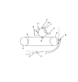
図1は実施例1で対象としている一般に使用されている二次転写方式の画像形成装置の作像部の概略構成を示す図である。同国において、画像形成装置の作像部は感光体ドラム1と、感光体ドラム1上に形成されたトナー像が一次転写装置2によって転写される中間転写ベルト3と、この中間転写ベルト3が張設される1対のローラ4,5対と、このローラ4,5対の一方、例えば従動側のローラ5に対向して設けられた二次転写装置6とから基本的に構成されている。感光体ドラム1の外周には、回転方向に沿って帯電装置7、現像装置8、一次転写装置2、クリーニング装置9及び除電装置10が設けられ、前記二次転写装置6と前記従動ローラ5との間には、図示しない給紙装置から伸びる用紙経路11が設けられている。
FIG. 1 is a diagram illustrating a schematic configuration of an image forming unit of a generally used secondary transfer type image forming apparatus which is a target in the first embodiment. In this country, the image forming unit of the image forming apparatus includes a
このように大略構成された画像形成装置では、図示矢印方向に回転する感光体ドラム1の表面が帯電装置7によって帯電され、帯電された感光体ドラム1表面に光ビーム12が照射される。これにより、感光体ドラム1の表面に静電潜像が形成される。形成された静電潜像は現像装置8によってトナー現像され、トナー像が感光体ドラム1表面に形成される。中間転写ベルト3は感光体ドラム1表面と一次転写装置2位置で接触しており、前記トナー像が一次転写装置2位置に至ると、一次転写装置2の転写バイアスによって感光体ドラム1表面のトナー像は中間転写ベルト3上に転写される。
In the image forming apparatus generally configured as described above, the surface of the
中間転写ベルト3に転写された画像は中間転写ベルト3の図示矢印方向の回転により従動ローラ5側に至り、前記給紙装置側から用紙経路11に沿って搬送されてきた用紙はレジストローラ13位置から前記画像先端とタイミングを取って送り出される。そして、二次転写装置6位置で画像先端と用紙先端が揃った状態になり、用紙の搬送に伴って中間転写ベルト3上の画像が用紙上に転写される。転写された画像は図示しない定着装置によって定着され、機外に排出される。
The image transferred to the intermediate transfer belt 3 reaches the driven
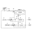
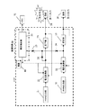
図2は図1の画像形成装置の高圧電源回路HVPの概略構成を示すブロック図である。同図において、並列に設けられた第1及び第2の負荷20,30に対してそれぞれ電源が供給される。電源の供給は第1の負荷20に対しては、直列に設けられた第1のPWM入力部21、第1のPWM入力部21からの入力に基づいて電源40から供給される電源電圧を変換する第1の電圧変換部22、第1の電圧変換部22で変換された電圧を昇圧して第1の負荷に供給する昇圧部23によって行われ、第2の負荷30に対しても直列に設けられた同様の構成の第2のPWM入力部31、第2の電圧変換部32及び第2の昇圧部33によって行われる。なお、第1及び第2の昇圧部23,33の下流側(二次側)の出力は第1及び第2の昇圧変換部22,23にフィードバックされている。第1及び第2の昇圧部23,33の上流側(一次側)にはそれぞれ第1及び第2のエラー検出電圧発生部a,bが接続され、第1及び第2のエラー検出電圧発生部a,bの出力は保護回路50に導かれる。この接続回路には第1及び第2のダイオード24,34がそれぞれ並列に設けられ、第1及び第2のダイオード24,34と保護回路50との間には前記ダイオード24,34と直列にツェナーダイオード25が接続されている。なお、保護回路50には異常検出部51が設けられている。
FIG. 2 is a block diagram showing a schematic configuration of the high-voltage power supply circuit HVP of the image forming apparatus of FIG. In the figure, power is supplied to first and
すなわち、ツェナーダイオードは異常検出部側がアノード、信号の入力側がカソードとなるように第11及び第2の出力のエラー検出電圧発生部a,bからの信号線に接続され、前記第1及び第2の出力のエラー検出電圧発生部a,bは前記第1及び第2のダイオード24,34のカソード側を1つにまとめ、前記ツェナーダイオードのカソードと接続している。なお、電源40は外部電源装置41から電源の供給を受ける。
That is, the Zener diode is connected to the signal lines from the first and second output error detection voltage generation units a and b so that the abnormality detection unit side is an anode and the signal input side is a cathode. The output error detection voltage generators a and b of the first and
このように構成された高圧電源回路HVPでは、第1及び第2のエラー検出電圧発生部a,bが前述のように接続されていることから、第1及び第2のエラー検出電圧発生部a,bどちらかの電圧が15V以上となったとき、保護回路50内の異常検出部51に電流が流れる。保護回路50はこの電流によってエラーを検知し、高圧電源基板上にある電圧変換部22,23の電源を落とし、たとえPWM信号が入力されても高圧出力を停止させる。なお、電圧変換部22,23はICによって構成されている。
In the high voltage power supply circuit HVP configured as described above, the first and second error detection voltage generators a and b are connected as described above. , B when the voltage becomes 15 V or more, a current flows through the
このように本実施例によれば、エラーを信号で見るのではなく各エラー検出電圧発生部a,bが一定の電圧以下であるという条件で電圧を監視することによって保護回路として1つにまとめることができる。その結果、複数の出力に対しても単一の保護回路50(異常検出部51)で検知できる構成とすることが可能となり、省コスト及び省スペース化に有利になる。 As described above, according to the present embodiment, the error is not observed as a signal, but the error detection voltage generators a and b are combined into one protection circuit by monitoring the voltage under the condition that the voltage is not more than a certain voltage. be able to. As a result, a configuration in which a single protection circuit 50 (abnormality detection unit 51) can detect a plurality of outputs can be obtained, which is advantageous for cost and space saving.
また、エラー検出電圧発生部a,bを昇圧部23,33の一次側に配置したので、高圧になる前の電圧で異常検知することが可能となる。これにより耐圧の高い部品を使用する必要がなくなり、コスト的に優位となる。
Further, since the error detection voltage generators a and b are arranged on the primary side of the
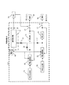
図3は実施例2に係る高圧電源回路HVPの槻略構成を示すブロック図である。この実施例は、実施例1に対して第1及び第2のエラー検出電圧発生部a,bをそれぞれ第1及び第2の昇圧部23,33の二次側に配置した例である。画像形成装置自体、及び高圧電源回路HVPは、第1及び第2のエラー検出電圧発生部a,bの配置を除いて実施例1と同等に構成され、保護回路50も第1及び第2のエラー検出電圧発生部a,bの検知出力によって同一の動作を行う。
FIG. 3 is a block diagram illustrating a schematic configuration of the high-voltage power supply circuit HVP according to the second embodiment. This embodiment is an example in which the first and second error detection voltage generators a and b are arranged on the secondary side of the first and
なお、第1及び第2のエラー検出電圧発生部a,bは昇圧後の電圧を検知することから、図示していないが、実機では抵抗などで分圧し、所定の電圧まで落とした電圧が保護回路50に入力するようにしてある。その他、特に説明しない各部は実施例1と同等に構成され、同等に機能する。 Since the first and second error detection voltage generators a and b detect the boosted voltage, although not shown in the figure, the actual machine divides the voltage with a resistor and protects the voltage dropped to a predetermined voltage. The signal is input to the circuit 50. Other parts not specifically described are configured in the same manner as in the first embodiment and function in the same manner.
このように本実施例によれば、第1及び第2のエラー検出電圧発生部a,bを第1及び第2の昇圧部23,33の二次側に配置下ので、昇圧の際の誤差(トランスの公差等)に関係なく、負荷にかかる電圧(実機では降圧した電圧)を直接異常検出部51に入力することができる。これにより、実施例1に比べて異常検出電圧をよりシビアに検出することが可能となる。
As described above, according to the present embodiment, the first and second error detection voltage generation units a and b are arranged on the secondary side of the first and second boosting
図4は実施例3に係る高圧電源回路HVPの概略構成を示すブロック園である。この実施例は、実施例1では、異常発生時に保護回路50がlC電源40から電圧変換部22,32に供給する電源をオフするように構成したものを、外部電源装置60からlC電源40に供給される電源をオフするように構成したものである。
FIG. 4 is a block diagram showing a schematic configuration of the high-voltage power supply circuit HVP according to the third embodiment. In this embodiment, in the first embodiment, the protection circuit 50 is configured to turn off the power supplied from the
これにより異常が発生したとき、外部電源装置60からlC電源40に供給される電源がオフされ、1C電源40への電源の供給が行われなくなる。その結果、電圧変換部22,32への電源供給が停止され、高圧電源回路HVPからの高圧出力が停止される。
Thus, when an abnormality occurs, the power supplied from the
その他、特に説明しない各部は実施例1と同等に構成され、同等に機能する。 Other parts not specifically described are configured in the same manner as in the first embodiment and function in the same manner.
図5は実施例4に係る高圧電源回路HVPの槻略構成を示すブロック図である。この実施例は、実施例1に対して外部、ここではCPU70にエラー信号を出力することができるように構成した例で、高圧電源回路HVP自体は実施例1と同一である。
FIG. 5 is a block diagram illustrating a schematic configuration of a high-voltage power supply circuit HVP according to the fourth embodiment. This embodiment is an example in which an error signal can be output to the outside, here, the
図6は保護回路50内のエラー信号の外部出力に関する回路構成を示すブロック図である。保護回路50は第1ないし第3のスイッチ52,53,54を備えている。第2及び第3のスイッチ53,54は第1のスイッチ52に対して並列に接続され、第2のスイッチ53はlC電源Vddに、第3のスイッチ54はCPU70側への制御電源回路26に接続されている。その他、特に説明しない各部は実施例1と同等に構成され、同等に機能する。
FIG. 6 is a block diagram showing a circuit configuration relating to the external output of the error signal in the protection circuit 50. The protection circuit 50 includes first to
この実施例では、保護回路50においてツェナーダイオード25を貫通して電流が流れた場合に、図6に示すように第1のスイッチ52がオンされ、そのオン信号を受けて第2及び第3のスイッチ53,54が同時にオンするような回路構成をとっている。これにより異常検出時に高圧出力停止の保護動作と同時にCPU70へエラーを知らせる信号27を追加する構成となり、画像形成装置全体の動きを停止させるとともに、ユーザーにその旨知らせることが可能となる。
In this embodiment, when a current flows through the
なお、画像形成装置全体の動きを停止させることに代えて、高圧基板へ入力しているPWMを停止させることにより電源供給を停止させることも可能である。 Instead of stopping the movement of the entire image forming apparatus, it is also possible to stop power supply by stopping PWM input to the high voltage substrate.
前記実施例1ないし4記載の発明では、複数の負荷を有する高圧電源に対し、
負荷数=エラー検知部
ではなく負荷数にかかわらずエラー信号を1つにまとめる構成をとることによってコスト及びスペース的に有利となっている。しかし、実施例1ないし4記載の発明の構成のみでは異常検出部51を1つにしたためにエラー発生時に、どの負荷においてエラーが発生しているかは不明であった。そのため、エラー発生時ユーザーあるいはサービスマンは全ての出力に対し検査し、エラーを生じた負荷を見つける必要があった。
In the inventions according to the first to fourth embodiments, for a high-voltage power supply having a plurality of loads,
It is advantageous in terms of cost and space by adopting a configuration in which error signals are combined into one regardless of the number of loads instead of the number of loads = error detection unit. However, with only the configuration of the invention described in the first to fourth embodiments, it is not clear in which load an error has occurred when an error occurs because there is only one
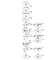
そこで、本実施例では、実施例1ないし4の構成のままで、エラー発生個所を特定できるようにした。図7は実施例5におけるエラー発生個所の特定処理の処理手順を示すフローチャートである。 Therefore, in this embodiment, it is possible to specify the location where an error has occurred with the configuration of the first to fourth embodiments. FIG. 7 is a flowchart illustrating a processing procedure for specifying an error occurrence location in the fifth embodiment.
すなわち、実施例4の図5に示した構成において、エラー発生時に復帰までの間に「第1の出力(例えば第1の負荷20)のみon」→「第2の出力(例えば第2の負荷30)のみon」という制御ステップを設けることによりどの出力でエラーが発生しているのかを特定することができる。 That is, in the configuration shown in FIG. 5 of the fourth embodiment, “only the first output (for example, the first load 20) is turned on” → “the second output (for example, the second load) before the return when an error occurs. By providing a control step of “30) only on”, it is possible to specify which output causes the error.
具体的には、図7において、エラーが発生すると(ステップS101)、全出力を停止させ(ステップS102)、その後、第1出力(負荷20)をonする(ステップS103)。この状態でエラー発生があるかどうかをチェックする(ステップS104)。エラー発生があれば、エラー発生個所を特定し(ステップS105)、特定したエラー個所をユーザーに表示する(ステップS106)。次いで、第1出力(負荷20)をoff、第2出力(負荷30)をonした(ステップS107)後、エラー発生の有無をチェックする(ステップS108)。一方、ステップS104でエラーが発生していなければ、ステップS107にスキップし、ステップS107の処理を実行する。 Specifically, in FIG. 7, when an error occurs (step S101), all outputs are stopped (step S102), and then the first output (load 20) is turned on (step S103). It is checked whether an error has occurred in this state (step S104). If there is an error, the location where the error occurred is specified (step S105), and the specified error location is displayed to the user (step S106). Next, after the first output (load 20) is turned off and the second output (load 30) is turned on (step S107), whether or not an error has occurred is checked (step S108). On the other hand, if no error has occurred in step S104, the process skips to step S107 and executes the process of step S107.
ステップS108のチェックで、エラーが発生していれば、エラー発生個所を特定し(ステップS109)、特定したエラー個所をユーザーに表示する(ステップS110)。その後、第2出力をoff、第3出力をonというように、各出力について順次off、onを繰り返してエラー位置を特定し、第n出力までくると、第(n−1)出力をoff、第n出力をonして(ステップS111)、エラー発生の有無をチェックする(ステップS112)。そして、エラー発生があれば、エラー発生個所を特定し(ステップS113)、特定したエラー個所をユーザーに表示し(ステップS114)、処理を終える。また、ステップS112でエラー発生がなければ、そのまま処理を終える。 If an error has occurred in the check in step S108, the error location is specified (step S109), and the specified error location is displayed to the user (step S110). After that, the second output is turned off, the third output is turned on, and the error position is identified by repeating off and on sequentially for each output. When the output reaches the nth output, the (n−1) th output is turned off, The n-th output is turned on (step S111), and whether or not an error has occurred is checked (step S112). If an error has occurred, the error location is identified (step S113), the identified error location is displayed to the user (step S114), and the process ends. If no error occurs in step S112, the process is finished as it is.
例えば、図8に示すように第1出力(第1の負荷20)に異常が発生した場合、図7のフローチャートに示したような制御処理を行わないときには、どの部分(出力個所)で異常が発生したか特定できないまま、高圧電源を止めることになる。しかし、図7のフローチャートに示したように各出力を個別に順次出力し、エラーチェックを行うことにより、エラー個所が特定できる。また、複数の出力に異常が発生した場合も、第1出力の異常表示後、他の出力に異常がないかチェックするので、全ての出力の異常検出が可能となる。 For example, when an abnormality occurs in the first output (first load 20) as shown in FIG. 8, when the control process as shown in the flowchart of FIG. The high-voltage power supply will be stopped without knowing if it has occurred. However, as shown in the flowchart of FIG. 7, each output is sequentially output individually and an error check is performed, whereby the error location can be specified. Further, even when an abnormality occurs in a plurality of outputs, it is possible to detect an abnormality in all the outputs since the other outputs are checked for abnormality after the first output abnormality is displayed.
その他、特に説明しない各部は図5に示した第4の実施例と同等に構成されているので、重複する説明は省略する。 Other parts that are not specifically described are configured in the same way as the fourth embodiment shown in FIG.
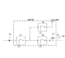
高圧電源の使用用途においては図9に示すように全体のシステムの構成上、第1出力の負荷20と第2出力の負荷30同士が負荷60を通してつながった経路をもつ場合がある。例えば、画像形成装置における帯電出力と現像出力は感光体を通して高圧電源の負荷同士につながった経路がある。このような構成の場合、各出力を個別に出力させてもエラーにはならないが、つながった経路を有し、かつ、その負荷を通してつながっている出力の極性が違うときには複数の出力を同時にonすることによりエラーが発生する可能性もある。図9では、第1出力20の極性がマイナスで第2出力30の極性がプラスの例を示している。
In the usage application of the high-voltage power supply, as shown in FIG. 9, the
図10は、このように高圧電源の負荷同士がつながった高電圧負荷の場合に好適なエラー発生個所の特定処理の処理手順を示すフローチャートである。 FIG. 10 is a flowchart showing a processing procedure for specifying the error occurrence portion, which is suitable for a high voltage load in which loads of the high voltage power supply are connected in this way.
このフローチャートでは、図7のフローチャートのステップS107に代えてステップS107aとし、また、ステップS111に代えてステップS111aとしたものである。ステップS107aでは第1出力(負荷20)on、第2出力(負荷30)onとし、ステップS111aでは、第1出力on、第2出力on・・・第n出力onというように各出力(負荷)を重畳させてエラー発生をチェック(ステップS112)するもので、個別ではエラーが発生しない場合においてもエラー個所を特定することができる。 In this flowchart, step S107a is substituted for step S107 in the flowchart of FIG. 7, and step S111a is substituted for step S111. In step S107a, the first output (load 20) is turned on and the second output (load 30) is turned on. In step S111a, the first output on, the second output on. Are overlapped to check the occurrence of an error (step S112), and an error location can be specified even when an error does not occur individually.
その他、特に説明しない各部及び各ステップは実施例5と同等に構成され、同等に機能する。 In addition, each part and each step not specifically described are configured in the same manner as in the fifth embodiment and function in the same manner.
図11は実施例7におけるエラー発生個所の特定処理の処理手順を示すフローチャートである。このフローチャートは、実施例5と実施例6を組み合わせたもので、ステップS101からステップS114までは実施例5の順次出力のステップで処理し、その後、ステップS201からステップS208までの実施例2の重畳出力のステップで処理するフローチャートである。このフローチャートでは、ステップS107からステップS111で各出力を順次onしてエラー検知を行い、ステップS201からステップS205で各出力を重畳してonし、エラー検知を行っている。 FIG. 11 is a flowchart illustrating a processing procedure for specifying an error occurrence location in the seventh embodiment. This flowchart is a combination of the fifth embodiment and the sixth embodiment. Steps S101 to S114 are processed in the sequential output steps of the fifth embodiment, and then the superimposition of the second embodiment from the step S201 to the step S208 is performed. It is a flowchart processed in the step of output. In this flowchart, each output is sequentially turned on in steps S107 to S111 to detect an error, and each output is superimposed and turned on in steps S201 to S205 to perform error detection.
このように複数の出力を有する場合には、図8に示した高圧電源及び図9に示した高圧電源の両方でエラーが発生する可能性がある。しかし、図11のフローチャートで示したように処理することにより、図8及び図9の構成が混同している回路構成においてもエラー発生個所を特定することができる。その他、特に説明しない各部は前記実施例5及び6と同等に構成され、同等に機能する。 In the case of having a plurality of outputs in this way, an error may occur in both the high-voltage power source shown in FIG. 8 and the high-voltage power source shown in FIG. However, by performing the processing as shown in the flowchart of FIG. 11, it is possible to identify the location where the error occurs even in the circuit configuration in which the configurations of FIGS. 8 and 9 are confused. Other parts that are not particularly described are configured in the same manner as the fifth and sixth embodiments and function in the same manner.
図12は実施例8に係る高圧電源回路HVPの概略構成を示すブロック図である。この実施例は、実施例4のCPU70がPWM入力部21,31にそれぞれ制御信号を出力し、各出力に対する入力信号を制御するように構成したものである。その他の各部は実施例4と同等に構成され、同等に機能する。
FIG. 12 is a block diagram illustrating a schematic configuration of the high-voltage power supply circuit HVP according to the eighth embodiment. In this embodiment, the
これにより、前記実施例5ないし7の制御を実現することができる。 Thereby, control of the said Example 5 thru | or 7 is realizable.
図13は実施例9に係る高圧電源回路HVPの概略構成を示すブロック図である。この実施例は、実施例4の第1出力(負荷20)及び第2出力(負荷30)の直前に前記各出力20,30への電源供給のon/offを設定する手段、ここではスイッチ27,37を設け、CPU70が電源供給のon/offを設定できるようにしたものである。その他の各部は実施例4と同等に構成され、同等に機能する。
FIG. 13 is a block diagram illustrating a schematic configuration of the high-voltage power supply circuit HVP according to the ninth embodiment. This embodiment is a means for setting on / off of power supply to each of the
これにより、前記実施例5ないし7の制御を実現することができる。 Thereby, control of the said Example 5 thru | or 7 is realizable.
図14は実施例10に係る高圧電源回路HVPの槻略構成を示すブロック図である。この実施例は、実施例8と実施例9を組み合わせ、CPU70によってPWM入力部21,31への入力信号の制御、第1出力(負荷20)、第2出力(負荷30)への電源供給のon/off制御を行うことができるように構成したものである。その他の各部は実施例4と同等に構成され、同等に機能する。
FIG. 14 is a block diagram illustrating a schematic configuration of the high-voltage power supply circuit HVP according to the tenth embodiment. In this embodiment, the eighth embodiment and the ninth embodiment are combined, and the
これにより、前記実施例5ないし7の制御を実現することができる。 Thereby, control of the said Example 5 thru | or 7 is realizable.
以上のように、前述の実施形態によれば、
1)エラーを信号で見るのではなく各エラー検出電圧発生部が一定の電圧以下であるという条件で電圧を監視することによって保護回路を1つにまとめることができる。
2)複数の出力に対しても保護回路(異常検出部)を単一の構成とすることができるので、省コスト化と省スペース化を図ることができる。
3)第1及び第2のエラー検出電圧発生部a,bを第1及び第2の昇圧部23,33のそれぞれ一次側に配置することにより、高圧になる前の電圧で異常検知を行うことができる。
4)高圧になる前の電圧で異常検知を行うことができるので、耐圧の高い部品を使用する必要がなく、低コストで提供することができる。
5)第1及び第2のエラー検出電圧発生部a,bをそれぞれ第1及び第2の昇圧部23,33の二次側に配置することにより、昇圧の際の誤差(トランスの公差等)に関係なく、負荷にかかる電圧を保護回路(異常検出部)に直接入力するので、異常検出電圧をよりシビアに検出することが可能となる。
6)異常検出時に高圧出力停止の保護動作と同時にCPUへエラーを知らせる信号を追加することができるので、画像形成装置全体の動きを停止させると同時に、ユーザーに異常を知らせることが可能となる。
7)エラー発生から復帰までの間に出力を順次個別に出力するので、第1出力の負荷と第2出力の負荷同士が負荷を通してつながった経路をもたない場合においても、エラー検知部が1つにまとめられた構成を持つ場合においてもエラー発生個所を特定することができる。
8)エラー発生から復帰までの間に出力を重畳的に出力するので、第1出力の負荷と第2出力の負荷同士が負荷を通してつながった経路をもつ場合においても、エラー検知部が1つにまとめられた構成を持つ場合においてもエラー発生個所を特定することができる。 9)エラー発生から復帰までの間に出力を順次個別に出力後、出力を重畳的に出力するので、第1出力の負荷と第2出力の負荷同士が負荷を通してつながっている経路が併設されている場合回路構成においても、エラー検知部が1つにまとめられた構成を持つ場合においてもエラー発生個所を特定することができる。
10)出力制御を各出力毎に行うので、従来のものからハード的構成を変えることなくエラー発生個所を特定することができる。
11)各出力の直前にスイッチのような機構を設け、そのスイッチを制御することにより、エラー検知部が1つにまとめられた構成を持つ場合においてもエラー発生個所を特定することができる。
12)各出力に対する入力信号を制御するのではなく、各出力に対する入力信号及び各出力の直前にスイッチのような機構を設けそのスイッチを制御することで、異常発生個所が高圧電源外部の負荷なのか、高圧電源内部の入力−出力間の経路のものなのかまでも特定することができる。
等の効果を奏する。
As described above, according to the above-described embodiment,
1) The protection circuit can be integrated into one by monitoring the voltage under the condition that each error detection voltage generator is not more than a certain voltage, instead of looking at the error as a signal.
2) Since the protection circuit (abnormality detection unit) can be configured in a single configuration even for a plurality of outputs, cost saving and space saving can be achieved.
3) By arranging the first and second error detection voltage generators a and b on the primary sides of the first and
4) Since abnormality detection can be performed with a voltage before high voltage, it is not necessary to use parts with high withstand voltage, and can be provided at low cost.
5) By arranging the first and second error detection voltage generation units a and b on the secondary side of the first and second boosting
6) Since it is possible to add a signal notifying the CPU simultaneously with the high voltage output stop protection operation when an abnormality is detected, it is possible to stop the movement of the entire image forming apparatus and simultaneously notify the user of the abnormality.
7) Since the outputs are sequentially output individually from the occurrence of the error to the return, even if the load of the first output and the load of the second output do not have a path connected through the load, the
8) Since the output is output in a superimposed manner between the occurrence of the error and the return, even when the load of the first output and the load of the second output have a path connected through the load, only one error detection unit is provided. Even in the case of a combined configuration, it is possible to specify the location where an error occurs. 9) Since the output is output in a superimposed manner after the outputs are output individually and sequentially from the occurrence of the error to the return, a path is provided along which the load of the first output and the load of the second output are connected through the load. Even in the case of the circuit configuration, it is possible to identify the location where the error has occurred even when the error detection unit has a single configuration.
10) Since the output control is performed for each output, it is possible to specify the location where an error has occurred without changing the hardware configuration from the conventional one.
11) A mechanism such as a switch is provided immediately before each output, and by controlling the switch, it is possible to specify the location where an error has occurred even when the error detection unit has a single configuration.
12) Instead of controlling the input signal for each output, a mechanism such as a switch is provided immediately before the input signal for each output and each output, and the switch is controlled so that the location where the abnormality occurs is a load outside the high-voltage power supply. Or the path between the input and output in the high-voltage power supply.
There are effects such as.
1 感光体ドラム
2 一次転写装置
3 中間転写ベルト
4,5 ローラ対
6 二次転写装置
7 帯電装置
8 現像装置
9 クリーニング装置
10 除電装置
11 用紙経路
20,30 負荷
21,31 PWM入力部
22,32 電圧変換部
23,33 昇圧部
24,34 ダイオード
25 ツェナーダイオード
26 制御電源回路
27,37 スイッチ
40 電源
50 保護回路
51 異常検出部
52,53,54 スイッチ
60 外部電源装置
70 CPU
a,b エラー検出電圧発生部
HVP 高圧電源回路
DESCRIPTION OF
a, b Error detection voltage generator HVP High voltage power supply circuit
Claims (17)
異常時に前記出力を停止させる単一の保護回路と、
を備え、
前記保護回路は異常が発生したとき、前記複数の出力の全てを停止させることを特徴とする高圧電源装置。 Multiple outputs that can be set to different output voltages,
A single protection circuit that stops the output in the event of an abnormality;
With
The protection circuit stops all of the plurality of outputs when an abnormality occurs.
前記複数の出力が第1の出力及び第2の出力の2出力であって、
前記第1の出力及び第2の出力のそれぞれの異常を電圧によって検出する第1及び第2のエラー検出電圧発生部を備え、
前記保護回路へは前記第1及び第2のエラー検出電圧発生部からの電圧が入力されることを特徴とする高圧電源装置。 The high voltage power supply device according to claim 1,
The plurality of outputs are two outputs of a first output and a second output,
A first and second error detection voltage generator for detecting each abnormality of the first output and the second output by a voltage;
The high-voltage power supply apparatus according to claim 1, wherein voltages from the first and second error detection voltage generators are input to the protection circuit.
前記保護回路への前記第1及び第2のエラー検出電圧発生部からの電圧はツェナーダイオードを介して入力されることを特徴とする高圧電源装置。 The high voltage power supply device according to claim 2,
The high-voltage power supply apparatus according to claim 1, wherein voltages from the first and second error detection voltage generation units to the protection circuit are input via a Zener diode.
前記保護回路内の異常検出部への入力部に、当該異常検出部側がアノード、信号の入力側がカソードとなるようにツェナーダイオードを設け、
前記第1及び第2の出力のエラー検出電圧発生部を、ダイオードを通して1つにまとめ、前記ダイオードのカソード側を前記ツェナーダイオードのカソードと接続し、エラー検出電圧発生部の1つが予め設定された電圧以上になると前記異常検出部に信号が入力されることを特徴とする高圧電源装置。 The high voltage power supply device according to claim 1,
In the input part to the abnormality detection unit in the protection circuit, a Zener diode is provided so that the abnormality detection unit side is an anode and the signal input side is a cathode,
The error detection voltage generators of the first and second outputs are combined into one through a diode, the cathode side of the diode is connected to the cathode of the Zener diode, and one of the error detection voltage generators is preset. A high-voltage power supply apparatus, wherein a signal is input to the abnormality detection unit when the voltage exceeds a voltage.
前記保護回路は前記出力を停止させる際、出力電圧の値を制御する制御手段の電源を落とすことを特徴とする高圧電源装置。 In the high voltage power supply device according to any one of claims 1 to 4,
The high-voltage power supply apparatus according to claim 1, wherein when the output is stopped, the protection circuit powers down a control unit that controls a value of the output voltage.
前記保護回路は前記出力を停止させる際、高圧電源入力電圧を落とすことを特徴とする高圧電源装置。 In the high voltage power supply device according to any one of claims 1 to 4,
The high-voltage power supply apparatus according to claim 1, wherein the protection circuit drops the high-voltage power supply input voltage when stopping the output.
前記保護回路は前記出力の停止と同時にCPUへ異常を知らせる信号を出力することを特徴とする高圧電源装置。 The high voltage power supply device according to any one of claims 1 to 6,
The high-voltage power supply apparatus, wherein the protection circuit outputs a signal notifying the CPU of the abnormality simultaneously with the stop of the output.
前記第1及び第2のエラー検出電圧発生部が昇圧部の一次側に配置されていることを特徴とする高圧電源装置。 The high voltage power supply device according to any one of claims 2 to 4,
The high-voltage power supply apparatus according to claim 1, wherein the first and second error detection voltage generation units are arranged on a primary side of the boosting unit.
前記第1及び第2のエラー検出電圧発生部が昇圧部の二次側に配置されていることを特徴とする高圧電源装置。 The high voltage power supply device according to any one of claims 2 to 4,
The high-voltage power supply apparatus according to claim 1, wherein the first and second error detection voltage generators are arranged on the secondary side of the booster.
前記保護回路は前記複数の出力の全てを停止させた後、前記異常発生から復帰までの間に各出力を個別に出力させることを特徴とする高圧電源装置。 The high voltage power supply device according to claim 1,
The high-voltage power supply apparatus according to claim 1, wherein the protection circuit individually outputs each output between the occurrence of the abnormality and the return after stopping all of the plurality of outputs.
前記各出力を個別に出力させる際、前記各出力を個別に重畳することなく順次出力することを特徴とする高圧電源装置。 The high-voltage power supply device according to claim 10,
When outputting each said output separately, each said output is output sequentially, without superimposing separately, The high voltage power supply device characterized by the above-mentioned.
前記各出力を個別に出力させる際、前記各出力を順に重畳しながら出力することを特徴とする高圧電源装置。 The high-voltage power supply device according to claim 10,
When outputting each said output separately, outputting each said output, superimposing each said output in order.
前記各出力を個別に出力させる際、前記各出力を個別に重畳することなく順次出力し、その後、前記各出力を順に重畳しながら出力することを特徴とする高圧電源装置。 The high-voltage power supply device according to claim 10,
When outputting each said output separately, outputting each said output sequentially, without overlapping each other, and then outputting, outputting each said output in order.
前記各出力を個別に出力させる際、前記各出力に対する各入力信号を制御する手段を備えていることを特徴とする高圧電源装置。 The high voltage power supply device according to any one of claims 11 to 13,
A high-voltage power supply device comprising means for controlling each input signal for each output when each output is output individually.
前記各出力への供給電源を開閉するスイッチと、
前記各出力を個別に出力させる際、前記スイッチの開閉を制御する手段と、
を備えていることを特徴とする高圧電源装置。 The high voltage power supply device according to any one of claims 11 to 13,
A switch for opening and closing the power supply to each output;
Means for controlling opening and closing of the switch when outputting each of the outputs individually;
A high-voltage power supply device comprising:
前記第1の出力と異なる出力電圧を設定可能な第2の出力と、
を備え、
前記第1及び前記第2の出力の一方に異常が発生したとき、前記第1及び第2の出力の両方の出力を停止させることを特徴とする電源供給制御方法。 A first output;
A second output capable of setting an output voltage different from the first output;
With
A power supply control method, comprising: stopping an output of both the first and second outputs when an abnormality occurs in one of the first and second outputs.
Priority Applications (1)
| Application Number | Priority Date | Filing Date | Title |
|---|---|---|---|
| JP2007315005A JP2008172998A (en) | 2006-12-12 | 2007-12-05 | High-voltage power supply unit, image forming device, and power supply controlling method |
Applications Claiming Priority (2)
| Application Number | Priority Date | Filing Date | Title |
|---|---|---|---|
| JP2006334904 | 2006-12-12 | ||
| JP2007315005A JP2008172998A (en) | 2006-12-12 | 2007-12-05 | High-voltage power supply unit, image forming device, and power supply controlling method |
Publications (2)
| Publication Number | Publication Date |
|---|---|
| JP2008172998A true JP2008172998A (en) | 2008-07-24 |
| JP2008172998A5 JP2008172998A5 (en) | 2010-12-02 |
Family
ID=39700532
Family Applications (1)
| Application Number | Title | Priority Date | Filing Date |
|---|---|---|---|
| JP2007315005A Pending JP2008172998A (en) | 2006-12-12 | 2007-12-05 | High-voltage power supply unit, image forming device, and power supply controlling method |
Country Status (1)
| Country | Link |
|---|---|
| JP (1) | JP2008172998A (en) |
Cited By (4)
| Publication number | Priority date | Publication date | Assignee | Title |
|---|---|---|---|---|
| CN104085193A (en) * | 2014-07-08 | 2014-10-08 | 北京美科艺数码科技发展有限公司 | Spraying head protective circuit and spraying head control panel |
| US9535360B2 (en) | 2014-03-14 | 2017-01-03 | Ricoh Company, Limited | Image forming apparatus and emission control method for controlling pre-charge of light emitting elements of exposure units |
| JP2017126052A (en) * | 2016-01-13 | 2017-07-20 | 株式会社リコー | Image forming apparatus |
| US11194279B2 (en) | 2019-05-15 | 2021-12-07 | Ricoh Company, Ltd. | Power supply and image forming apparatus incorporating same |
Citations (5)
| Publication number | Priority date | Publication date | Assignee | Title |
|---|---|---|---|---|
| JPH03289321A (en) * | 1990-04-05 | 1991-12-19 | Ricoh Co Ltd | High-voltage power source apparatus |
| JPH0595668A (en) * | 1991-08-22 | 1993-04-16 | Canon Inc | Method for sensing abnormality of power supply equipment |
| JPH06284722A (en) * | 1993-03-30 | 1994-10-07 | Toshiba Lighting & Technol Corp | Dc power-supply device |
| JPH089632A (en) * | 1994-06-20 | 1996-01-12 | Fujitsu General Ltd | Switching regulator power unit |
| JPH11332001A (en) * | 1998-05-18 | 1999-11-30 | Toyota Motor Corp | Abnormality sensing device and method for dc-to-dc converter, and vehicle driving system having abnormality sensing function thereof |
-
2007
- 2007-12-05 JP JP2007315005A patent/JP2008172998A/en active Pending
Patent Citations (5)
| Publication number | Priority date | Publication date | Assignee | Title |
|---|---|---|---|---|
| JPH03289321A (en) * | 1990-04-05 | 1991-12-19 | Ricoh Co Ltd | High-voltage power source apparatus |
| JPH0595668A (en) * | 1991-08-22 | 1993-04-16 | Canon Inc | Method for sensing abnormality of power supply equipment |
| JPH06284722A (en) * | 1993-03-30 | 1994-10-07 | Toshiba Lighting & Technol Corp | Dc power-supply device |
| JPH089632A (en) * | 1994-06-20 | 1996-01-12 | Fujitsu General Ltd | Switching regulator power unit |
| JPH11332001A (en) * | 1998-05-18 | 1999-11-30 | Toyota Motor Corp | Abnormality sensing device and method for dc-to-dc converter, and vehicle driving system having abnormality sensing function thereof |
Cited By (4)
| Publication number | Priority date | Publication date | Assignee | Title |
|---|---|---|---|---|
| US9535360B2 (en) | 2014-03-14 | 2017-01-03 | Ricoh Company, Limited | Image forming apparatus and emission control method for controlling pre-charge of light emitting elements of exposure units |
| CN104085193A (en) * | 2014-07-08 | 2014-10-08 | 北京美科艺数码科技发展有限公司 | Spraying head protective circuit and spraying head control panel |
| JP2017126052A (en) * | 2016-01-13 | 2017-07-20 | 株式会社リコー | Image forming apparatus |
| US11194279B2 (en) | 2019-05-15 | 2021-12-07 | Ricoh Company, Ltd. | Power supply and image forming apparatus incorporating same |
Similar Documents
| Publication | Publication Date | Title |
|---|---|---|
| JP4548532B2 (en) | Power supply device and image forming apparatus provided with the device | |
| JP4386104B2 (en) | Image forming apparatus | |
| JP5573566B2 (en) | Image forming apparatus | |
| JP2008172998A (en) | High-voltage power supply unit, image forming device, and power supply controlling method | |
| US7574152B2 (en) | AC high-voltage device, image forming apparatus, and AC high-voltage output controlling method which restarts the AC high-voltage after an overload | |
| JP2010074956A (en) | Power supply apparatus and image forming apparatus | |
| US8391728B2 (en) | Image forming apparatus and voltage applying device comprising a control unit for controlling another control unit when the other control unit is abnormally restarted | |
| US8212380B2 (en) | Power source apparatus and image forming apparatus | |
| US8610315B2 (en) | Circuit and heating apparatus that completely cuts power to a supply circuit due to blowout of a fuse on a single supply line | |
| JP2012053168A (en) | Image forming apparatus | |
| US9944482B2 (en) | Motor control device, sheet conveying device, and image forming apparatus | |
| JP2006159740A (en) | Interlock system of image forming apparatus | |
| JP2010074887A (en) | Motor driving device, image forming apparatus, motor driving method, and computer program | |
| JP5212618B2 (en) | Image forming apparatus | |
| JP2008299203A (en) | Image forming apparatus | |
| JP2017017979A (en) | Motor control device, sheet conveyance device, image forming apparatus, and motor control method | |
| JP2014007818A (en) | Power supply device and image forming apparatus having the same | |
| JP2010197790A (en) | Image forming apparatus | |
| JP2004109166A (en) | Interlock system for image forming apparatus | |
| JP2017134207A (en) | Detection circuit and image formation device | |
| JP2010156730A (en) | Image forming apparatus | |
| JP4816775B2 (en) | Image forming apparatus and inspection method thereof | |
| US20110176827A1 (en) | Power supply apparatus, electrical equipment, and image forming apparatus | |
| JP6308906B2 (en) | High voltage power supply device and image forming apparatus using the same | |
| JP2006243542A (en) | Image forming apparatus |
Legal Events
| Date | Code | Title | Description |
|---|---|---|---|
| A711 | Notification of change in applicant |
Free format text: JAPANESE INTERMEDIATE CODE: A712 Effective date: 20081112 |
|
| A521 | Written amendment |
Free format text: JAPANESE INTERMEDIATE CODE: A523 Effective date: 20101019 |
|
| A621 | Written request for application examination |
Free format text: JAPANESE INTERMEDIATE CODE: A621 Effective date: 20101019 |
|
| A131 | Notification of reasons for refusal |
Free format text: JAPANESE INTERMEDIATE CODE: A131 Effective date: 20120424 |
|
| A977 | Report on retrieval |
Free format text: JAPANESE INTERMEDIATE CODE: A971007 Effective date: 20120425 |
|
| A521 | Written amendment |
Free format text: JAPANESE INTERMEDIATE CODE: A523 Effective date: 20120621 |
|
| A131 | Notification of reasons for refusal |
Free format text: JAPANESE INTERMEDIATE CODE: A131 Effective date: 20121120 |
|
| RD02 | Notification of acceptance of power of attorney |
Free format text: JAPANESE INTERMEDIATE CODE: A7422 Effective date: 20130322 |
|
| A02 | Decision of refusal |
Free format text: JAPANESE INTERMEDIATE CODE: A02 Effective date: 20130326 |