JP2008152192A - Developing device, process cartridge and image forming apparatus - Google Patents
Developing device, process cartridge and image forming apparatus Download PDFInfo
- Publication number
- JP2008152192A JP2008152192A JP2006342637A JP2006342637A JP2008152192A JP 2008152192 A JP2008152192 A JP 2008152192A JP 2006342637 A JP2006342637 A JP 2006342637A JP 2006342637 A JP2006342637 A JP 2006342637A JP 2008152192 A JP2008152192 A JP 2008152192A
- Authority
- JP
- Japan
- Prior art keywords
- developer
- toner
- developing
- developing device
- developing roller
- Prior art date
- Legal status (The legal status is an assumption and is not a legal conclusion. Google has not performed a legal analysis and makes no representation as to the accuracy of the status listed.)
- Granted
Links
Images


Abstract
Description
本発明は、記録材(記録媒体)上に画像を形成する機能を備えた、例えば、複写機、プリンタ、あるいは、ファクシミリ装置などの電子写真方式の画像形成装置に関する。さらに詳しくは、これらの装置に備えられる現像装置、プロセスカートリッジに関する。 The present invention relates to an electrophotographic image forming apparatus having a function of forming an image on a recording material (recording medium) such as a copying machine, a printer, or a facsimile machine. More specifically, the present invention relates to a developing device and a process cartridge provided in these devices.
従来、画像形成装置においては、静電潜像担持体上に形成した静電潜像を、現像装置により現像剤像として可視化している。 Conventionally, in an image forming apparatus, an electrostatic latent image formed on an electrostatic latent image carrier is visualized as a developer image by a developing device.
このような現像装置として、乾式一成分接触現像装置が提案され実用化されている。この場合、静電潜像担持体と現像剤担持体とを回転させ、適当な相対周速差で押圧若しくは接触させることで、静電潜像を現像している。加えて、磁性材料が不要であり、装置の簡略化及び小型化が容易である。また、非磁性現像剤を使用することでフルカラー画像形成装置に応用が可能である。 As such a developing device, a dry one-component contact developing device has been proposed and put into practical use. In this case, the electrostatic latent image bearing member and the developer bearing member are rotated and pressed or brought into contact with an appropriate relative peripheral speed to develop the electrostatic latent image. In addition, no magnetic material is required, and the apparatus can be easily simplified and downsized. Moreover, application to a full-color image forming apparatus is possible by using a nonmagnetic developer.
現像剤担持体としては、弾性及び導電性を有する現像ローラを使用することができる。接触現像装置では、静電潜像担持体に現像ローラを押圧若しくは接触させる。このため、静電潜像担持体が剛体である場合、静電潜像担持体を損傷させてしまう。これを避けるために、現像ローラを弾性体により構成する。また、現像ローラ表面若しくは表面近傍に導電層を設け、現像バイアスを印加して使用することもできる。 As the developer carrying member, a developing roller having elasticity and conductivity can be used. In the contact developing device, the developing roller is pressed or brought into contact with the electrostatic latent image carrier. For this reason, when the electrostatic latent image carrier is a rigid body, the electrostatic latent image carrier is damaged. In order to avoid this, the developing roller is made of an elastic body. Further, a conductive layer may be provided on the surface of the developing roller or in the vicinity of the surface, and a developing bias may be applied for use.
さらに、現像剤への電荷付与及び均一な現像剤層の形成を目的とし、現像剤担持体に現像剤規制部材として現像ブレードを当接させることも可能である。この場合、現像ブレードには、ゴム、又はバネ弾性を有する金属薄板で構成される。また、現像ブレードが導電性を持つ場合、現像ブレードを電源又はアースに接続して使用することもできる。 Further, for the purpose of imparting electric charge to the developer and forming a uniform developer layer, it is possible to bring a developing blade into contact with the developer carrying member as a developer regulating member. In this case, the developing blade is made of rubber or a metal thin plate having spring elasticity. Further, when the developing blade has conductivity, the developing blade can be used by being connected to a power source or a ground.
図5は従来の現像装置を示す図である。 FIG. 5 is a diagram showing a conventional developing device.
現像剤担持体である現像ローラ51は、シリコーン系ゴムを基層とし、ウレタン系ゴムを表層とする。この現像ローラ51は、導電性を有する弾性ローラであり、矢印C方向に回転駆動する。現像ブレード52は、導電性を持った金属ブレードであり、ブレード支持板金53に支持される。この現像ブレード52は、自由端側の先端近傍を現像ローラ51の外周面に面接触するように当接されている。このとき、現像ローラ51の表面にコートされたトナー層は現像ブレード52との摩擦により摩擦帯電される。
The developing
さらに、弾性ローラ54が現像ローラ51に当接し、矢印D方向に回転駆動する。この弾性ローラ54はスポンジローラであり、現像ローラ51へトナーの供給、かつ、現像されずに現像ローラ上に残ったトナーの剥ぎ取り行う。この弾性ローラ54は、現像ブレード52よりも、現像ローラ51の回転方向上流側に配設されている。トナー55は、非磁性一成分現像剤である。トナーの帯電性及び、転写性の向上を目的として、適当な量の疎水性シリカを外添している。
Further, the
上述した構成の現像装置において、現像ブレードはトナーへの摩擦帯電及び均一なトナー層の形成を達成し、良好に現像することができる。 In the developing device having the above-described configuration, the developing blade achieves triboelectric charging to the toner and formation of a uniform toner layer, and can be developed satisfactorily.
なお、関連する従来例が開示された文献としては、特許文献1がある。
しかしながら、現像ブレードが導電性を持ち、電源又はアースに接続される場合、摩擦によってトナー層に付与された摩擦帯電量は、現像ブレードを通して放電される場合がある。 However, when the developing blade has conductivity and is connected to a power source or ground, the triboelectric charge applied to the toner layer by friction may be discharged through the developing blade.
このため、摩擦によってトナー層に付与された摩擦帯電量が、放電によって減少するという問題が発生する場合がある。現像ローラの表面に形成されたトナー層の摩擦帯電量が減少すると、画像カブリ不良が発生する場合があるため、画像カブリ不良のない画像を得ることが要求されている。 For this reason, there may be a problem that the triboelectric charge applied to the toner layer by friction decreases due to discharge. When the triboelectric charge amount of the toner layer formed on the surface of the developing roller decreases, an image fogging defect may occur. Therefore, it is required to obtain an image having no image fogging defect.
さらに、高温高湿環境下においてはトナー表面及び内部に含まれる水分量は増加する。トナー表面及び内部に含まれる水分量が増加した場合、トナーが水分を介して現像ローラ表面に付着し、トナーと現像ローラ表面との摩擦機会は減少する。トナーと現像ローラ表面との摩擦機会が減少した場合、トナー層に付与される摩擦帯電量が減少する。つまり、トナー表面及び内部に含まれる水分量が増加することにより、トナーに付与される摩擦帯電量が減少し、画像カブリ不良が発生する場合がある。 Furthermore, the amount of water contained on the toner surface and inside increases in a high temperature and high humidity environment. When the amount of water contained in and on the toner surface increases, the toner adheres to the surface of the developing roller through the water, and the chance of friction between the toner and the developing roller surface decreases. When the chance of friction between the toner and the developing roller surface decreases, the amount of triboelectric charge applied to the toner layer decreases. That is, when the amount of water contained in and on the toner increases, the amount of triboelectric charge imparted to the toner decreases, and image fogging may occur.
本発明は上記したような事情に鑑みてなされたものであり、現像剤規制部材を導電性とした場合でも、現像剤の摩擦帯電量の変化を低減し、環境変化に対して影響の少ない画像特性及び信頼性に優れた装置を提供することを目的とする。 The present invention has been made in view of the above-described circumstances, and even when the developer regulating member is made conductive, the change in the triboelectric charge amount of the developer is reduced, and the image has less influence on environmental changes. An object is to provide an apparatus having excellent characteristics and reliability.
上記目的を達成するために本発明にあっては、
現像剤を担持搬送する現像剤担持体と、
前記現像剤担持体に圧接するように設けられ、前記現像剤担持体に担持された前記現像剤の量を規制する現像剤規制部材と、
を備え、
前記現像剤規制部材が導電性を有し、前記現像剤規制部材が導通部に電気的に導通される現像装置において、
前記現像剤担持体は、前記現像剤担持体表面の水に対する接触角が100度以上となるように設けられていることを特徴とする。
In order to achieve the above object, the present invention provides:
A developer carrier for carrying and conveying the developer;
A developer regulating member that is provided in pressure contact with the developer carrying member and regulates the amount of the developer carried on the developer carrying member;
With
In the developing device in which the developer regulating member has electrical conductivity, and the developer regulating member is electrically conducted to the conducting portion.
The developer carrying member is provided such that a contact angle with respect to water on the surface of the developer carrying member is 100 degrees or more.
本発明によれば、現像剤規制部材を導電性とした場合でも、現像剤の摩擦帯電量の変化を低減し、環境変化に対して影響の少ない画像特性及び信頼性に優れた装置を提供することが可能となる。 According to the present invention, even when the developer regulating member is made conductive, a change in the triboelectric charge amount of the developer is reduced, and an apparatus having excellent image characteristics and reliability with little influence on environmental changes is provided. It becomes possible.
以下に図面を参照して、この発明を実施するための最良の形態を例示的に詳しく説明する。ただし、この実施の形態に記載されている構成部品の寸法、材質、形状それらの相対配置などは、発明が適用される装置の構成や各種条件により適宜変更されるべきものであり、この発明の範囲を以下の実施の形態に限定する趣旨のものではない。 The best mode for carrying out the present invention will be exemplarily described in detail below with reference to the drawings. However, the dimensions, materials, shapes, and relative arrangements of the components described in this embodiment should be appropriately changed according to the configuration of the apparatus to which the invention is applied and various conditions. It is not intended to limit the scope to the following embodiments.
本発明では、現像剤規制部剤が導電性を有し、現像剤規制部材が導通部として、例えば電源又はアースに電気的に接続(導通)されるとき、現像剤担持体表面の水に対する接触角を100度以上とする構成を採用している。 In the present invention, when the developer regulating member has electrical conductivity and the developer regulating member is electrically connected (conductive) to the power source or the earth as the conducting portion, for example, the developer carrier surface is in contact with water. A configuration in which the angle is 100 degrees or more is adopted.
すなわち、現像剤規制部材が導電性であるため、現像剤層に付与された摩擦帯電量が現
像剤規制部材を通して放電された場合でも、摩擦機会の増加によって現像剤層に摩擦帯電量が付与されるため、画像カブリ不良の発生はない。
That is, since the developer regulating member is conductive, even when the triboelectric charge applied to the developer layer is discharged through the developer regulating member, the triboelectric charge is imparted to the developer layer due to an increase in the friction opportunity. Therefore, no image fogging defect occurs.
以下に、摩擦機会の増加による現像剤層への摩擦帯電量の付与について詳しく説明する。 Hereinafter, the application of the triboelectric charge amount to the developer layer due to an increase in the friction opportunity will be described in detail.
温度及び湿度等の環境変化に伴って、現像剤表面及び内部に含まれる水分量は変化する。現像剤表面及び内部に含まれる水分量が増加した場合、現像剤と現像剤担持体表面の付着力は増加する。ここで、現像剤担持体表面の水に対する接触角を100度以上にした場合、現像剤担持体表面は表面及び内部に水分を含んだ現像剤を弾く性質を持つ。このため、現像剤と現像剤担持体表面とが水分を介して付着しない。現像剤と現像剤担持体表面との付着を防いだ結果、現像剤と現像剤担持体表面との摩擦機会が増加し、現像剤に付与される摩擦帯電量が増加する。 As the environment changes such as temperature and humidity, the amount of water contained on the developer surface and inside changes. When the amount of water contained in and on the developer surface increases, the adhesion between the developer and the surface of the developer carrying member increases. Here, when the contact angle with respect to the water on the surface of the developer carrying member is set to 100 degrees or more, the surface of the developer carrying member has the property of repelling the developer containing moisture on the surface and inside. For this reason, the developer and the surface of the developer carrying member do not adhere via moisture. As a result of preventing adhesion between the developer and the surface of the developer carrier, the chance of friction between the developer and the surface of the developer carrier increases, and the amount of triboelectric charge imparted to the developer increases.
つまり、温度及び湿度等の環境変化に伴って、現像剤表面及び内部に含まれる水分量が増加した場合でも、現像剤の摩擦帯電量を増加させることができる。 That is, the triboelectric charge amount of the developer can be increased even when the amount of water contained on the surface and inside of the developer increases with environmental changes such as temperature and humidity.
この結果、摩擦帯電量が現像剤規制部材を通して放電された場合でも、現像剤担持体の表面に形成された現像剤層の摩擦帯電量が増加する。これにより、画像カブリ不良の発生が著しく低減し、環境変化に対して影響の少ない画像特性及び信頼性に優れた装置が得られるものである。 As a result, even when the triboelectric charge is discharged through the developer regulating member, the triboelectric charge of the developer layer formed on the surface of the developer carrier increases. As a result, the occurrence of image fogging defects is remarkably reduced, and an apparatus having excellent image characteristics and reliability with little influence on environmental changes can be obtained.
図1は本発明を適用した画像形成装置10の概略断面図、図2は本発明を適用した現像装置14の概略断面図である。まず、画像形成手段による画像形成動作について説明する。
FIG. 1 is a schematic sectional view of an
図1において、静電潜像担持体としての感光ドラム11は、矢印A方向に回転する。まず感光ドラム11は、帯電装置12によって一様に帯電される。その後、露光手段であるレーザ光学装置からのレーザ光13により露光され、その表面に静電潜像が形成される。この静電潜像を、感光ドラム11に所定の侵入量をもって押圧、接触するように配設された現像装置14によって現像し、現像剤像(トナー像)として可視化する(現像装置14は感光ドラム11に現像作用を行う)。可視化された感光ドラム11上のトナー像は、転写ローラ15によって記録材16に転写される。
In FIG. 1, a
転写されずに感光ドラム11上に残存した転写残トナーは、クリーニング部材であるクリーニングブレード17により掻き取られ、廃トナー容器18に収納される。クリーニングされた感光ドラム11は上述作用を繰り返し、画像形成を行う。一方、トナー像を転写された記録材16は、定着装置19によって永久定着された後、機外に排出される。
Untransferred toner remaining on the
現像装置14について、図2に基づき、さらに説明する。
The developing
図2において、21は、現像剤としての負帯電性の非磁性一成分トナー22(以下、単にトナーという場合もある)を収容する現像容器である。現像装置14は、現像容器21内の長手方向に延在する開口部に位置し、感光ドラム11と対向配置され現像剤担持体としてトナーを担持搬送する現像ローラ23を備え、感光ドラム11上の静電潜像を現像、可視化するようになっている。
In FIG. 2,
感光ドラム11は、アルミシリンダーを基体とし、その周囲に所定厚みの感光層を塗工した剛体である。画像形成時において、感光ドラム11は、帯電装置により帯電電位Vd
=−700Vに均一帯電されており、画像信号に従いレーザで露光された部分がVl=−150Vになる。Vl部に対し、現像ローラ23の芯金には直流電圧=Vdc=−300Vが、現像バイアスとして印加され、負性帯電トナーで反転現像される。
The
= -700V is uniformly charged, and the portion exposed by the laser according to the image signal becomes Vl = -150V. A DC voltage = Vdc = −300 V is applied as a developing bias to the core of the developing
弾性を有する現像ローラ23は、上記開口部にて、図に示す右略半周を現像容器21に突入し、左略半周面を現像容器21から露出して横設される。この現像容器21から露出した面は、現像装置14の左方に位置する感光ドラム11に所定の侵入量となるように押圧、接触するように対向している。本実施の形態においては、感光ドラム11に対して現像ローラ23が50μm侵入し、接触する。現像ローラ23は矢印B方向に回転駆動される。
In the opening, the developing
本実施例における現像ローラ23は、シリコーン系ゴムを基層とし、フッ素系ゴムを表層にコートした二層構成であり、その表面粗さ(算術平均粗さ(Ra))は、Ra=0.2μm、Rz=0.5μm、Rmax=0.7μmである。また、現像ローラ23は、104〜106Ωの抵抗を有している。現像ローラ23表層の水に対する接触角は、110度である。本実施例においては、表面及び内部に水分を含んだトナーに対して良好な撥水性を有する厚さ30μmのフッ素系ゴムで現像ローラ表層を構成している。
The developing
現像ローラ23の表層としては、フッ素系ゴムの他に、ナイロン系樹脂、シリコーン系樹脂、ウレタン系樹脂、アクリル系樹脂など水に対する接触角が100度以上となるならば、何れも好適に用いることができる。また、現像ローラの表層材料の変更ではなく、表層に対するコーティング、放電等を用いた表面改質などであっても、接触角を100度以上とするならば、何れも好適に用いることができる。接触角の測定は、協和界面科学の接触角計FACEを用い、現像ローラに対して1μL〜2μLの純水を滴下させ接触角を測定した。
As the surface layer of the developing
現像ローラ23の一方には、導電性、弾性を有する現像剤規制部材としての現像ブレード25が、支持板金26に支持され、自由端側の先端近傍を現像ローラ23の外周面に面接触にて当接(圧接)するように設けられている。現像ブレード25は現像ローラ23を線圧40g/cmで押圧し、現像ローラ23の表面に0.5mg/cm2のトナー層を均一に形成する。
On one side of the developing
現像ブレード25の材質として、本実施例では、導電性を有する厚さ80μmのステンレス薄板を用いる。その表面粗さは、Ra=0.1μm、Rz=0.5μm、Rmax=0.7μmである。当接方向としては、当接部に対して自由端側の先端が、現像ローラ23の回転方向上流側に位置するカウンター方向となっている。また、現像ブレード25にはブレードバイアス電源により、現像バイアスに対してV=Δ−200Vの直流電圧が印加される。ここで、ブレードバイアス電源は、電圧印加手段又は電源を構成している。
As a material of the developing
現像ローラ23のもう一方には、弾性ローラ24が当接され、回転可能に支持されている。弾性ローラ24は、スポンジ構造や、芯金上にレーヨン、ナイロン等の繊維を植毛したファーブラシ構造のものが、現像ローラ23へのトナー供給及び未現像トナーの剥ぎ取りの点から好ましい。本実施例においては、ウレタンスポンジローラであり、現像ローラ23と同一方向に回転駆動する。
An
本実施例において、一成分現像剤として負帯電性の非磁性一成分トナー22には、転写効率を向上させるため、略球形トナー(球形状のトナー、球形化処理されたトナー)を用いている。
In this embodiment, a substantially spherical toner (spherical toner, spheroidized toner) is used for the negatively chargeable nonmagnetic one-
トナーの製造方法としては、例えば従来の粉砕トナー表面を熱的・機械的ストレスによ
り塑性球形化処理することも可能である。また、混濁重合法により直接トナーを製造する方法や、単量体には可溶で得られる重合体が不溶な水系有機溶剤を用い、直接トナーを背生成する分散重合方法を用いることも可能である。また、水溶性極性開始剤存在下で直接重合しトナーを生成するソープフリー重合方法に代表される乳化重合法等を用いることも可能である。
As a toner manufacturing method, for example, a conventional pulverized toner surface can be subjected to plastic spheroidization treatment by thermal and mechanical stress. It is also possible to use a method of directly producing a toner by a turbid polymerization method, or a dispersion polymerization method in which an aqueous organic solvent that is soluble in the monomer and insoluble in the obtained polymer is used to directly produce the toner. is there. It is also possible to use an emulsion polymerization method represented by a soap-free polymerization method in which a toner is produced by direct polymerization in the presence of a water-soluble polar initiator.
本実施例においては、粒度分布がシャープな4〜8μmの粒径が得られる常圧下、又は、加圧下での混濁重合方法を用いている。そして、モノマーとしてスチレンとn−ブチルアクリレート、荷電制御剤としてサリチル酸金属化合物、極性レジンとして飽和ポリエステル、さらに着色剤を加えて次のようなトナーを製造している。すなわち、重量平均粒径約7μmであり、重量平均粒径4μm以下のトナー粒子が25個数%以下の負帯電性トナーを製造している。 In this example, a turbid polymerization method under normal pressure or under pressure in which a particle size distribution of 4 to 8 μm with a sharp particle size distribution is obtained is used. Then, styrene and n-butyl acrylate as monomers, a salicylic acid metal compound as a charge control agent, a saturated polyester as a polar resin, and a colorant are added to produce the following toner. That is, a negatively chargeable toner having a weight average particle diameter of about 7 μm and toner particles having a weight average particle diameter of 4 μm or less is 25% by number or less is manufactured.
その後、流動性付与剤として、疎水性シリカを1.5wt%外添している。外添量は、当然これに限るものではない。トナー表面を外添剤によって被膜することで、負性帯電性能の向上、かつ、トナー間に微小な間隙を設けることによる、流動性の向上を達成している。 Thereafter, 1.5 wt% of hydrophobic silica is externally added as a fluidity imparting agent. Of course, the amount of external addition is not limited to this. By coating the toner surface with an external additive, the negative charging performance is improved, and the flowability is improved by providing a minute gap between the toners.
以上説明した画像形成装置10と現像装置14を用いて、高温高湿環境(30℃、80%RH)に1日放置してプリントアウト試験を行った。その結果、画像カブリ不良が発生することなく高画質な画像を得ることができた。
Using the
以下に、本実施例について詳細な説明を行う。 In the following, this embodiment will be described in detail.
従来の現像装置を高温高湿環境(30℃、80%RH)に1日間放置して、プリントアウト試験を行ったところ、画像カブリ不良が発生した。反対に、従来の現像装置を低温低湿環境に1日間放置して、プリントアウト試験を行ったが、画像カブリ不良は発生しなかった。実験結果を表1と表2に示す。 When a conventional developing apparatus was left in a high temperature and high humidity environment (30 ° C., 80% RH) for 1 day and a printout test was performed, an image fogging defect occurred. On the other hand, the conventional developing device was left in a low temperature and low humidity environment for 1 day to conduct a printout test. However, no image fogging occurred. The experimental results are shown in Tables 1 and 2.

画像カブリ不良について詳細に調べた結果、高温高湿環境下、現像ブレードと現像ローラを等電位にする、現像ブレードを薄くする、現像ローラの回転速度を遅くする場合に画像カブリ不良は発生した。 As a result of examining image fog defects in detail, image fog defects occurred when the developing blade and the developing roller were equipotential, the developing blade was thinned, and the rotation speed of the developing roller was decreased in a high temperature and high humidity environment.
つまり、画像カブリ不良が発生する原因は、高温高湿環境下、現像ブレードと現像ローラを等電位にする、現像ブレードを薄くする、現像ローラの回転速度を遅くする場合に、現像ローラの表面に形成されたトナー層の摩擦帯電量が不足しているためであった。つまり、現像ブレードが導電性を有し、現像ブレードが導通部として電源又はアースに接続されるため、トナー層に付与された摩擦帯電量が現像ブレードを通して放電されるため、トナー層の摩擦帯電量が不足していた。 In other words, the cause of image fogging failure is the surface of the developing roller when the developing blade and developing roller are equipotential, the developing blade is thinned, or the developing roller is slowed down in a high temperature and high humidity environment. This is because the triboelectric charge amount of the formed toner layer is insufficient. In other words, since the developing blade has conductivity and the developing blade is connected to a power source or ground as a conducting portion, the triboelectric charge applied to the toner layer is discharged through the developing blade, so the triboelectric charge amount of the toner layer Was lacking.
詳しくは、高温高湿環境下においてトナー表面及び内部に含まれる水分量は増加する。トナー表面及び内部に含まれる水分量が増加した場合、トナーと現像ローラ表面の付着力は増加する。付着力が増加すると、トナーと現像ローラ表面との摩擦機会が減少し、トナー層の摩擦帯電量が減少していた。また、現像ブレードと現像ローラを等電位にする場合、トナー層に付与した摩擦帯電量が現像ブレードを通して放電され、摩擦帯電量が減少していた。また、現像ブレードを薄く、現像ローラの回転数を遅くした場合も、トナーと現像ブレード表面、トナーと現像ローラ表面、トナー同士の摩擦機会が減少し、トナー層に付与される摩擦帯電量が減少していた。 Specifically, the amount of water contained in the toner surface and inside increases in a high temperature and high humidity environment. When the amount of water contained in and on the toner surface increases, the adhesion between the toner and the developing roller surface increases. As the adhesive force increases, the chance of friction between the toner and the developing roller surface decreases, and the triboelectric charge amount of the toner layer decreases. Further, when the developing blade and the developing roller are equipotential, the triboelectric charge applied to the toner layer is discharged through the developing blade, and the triboelectric charge is reduced. Even when the developing blade is thin and the rotation speed of the developing roller is slowed, the chance of friction between the toner and the developing blade surface, the toner and the developing roller surface, and the toner decreases, and the amount of triboelectric charge applied to the toner layer decreases. Was.
このような高温高湿環境下、現像ブレードと現像ローラを等電位にする、現像ブレードを薄くする、現像ローラの回転速度を遅くする場合に摩擦帯電量は不足し、画像カブリ不良は発生していた。 In such a high temperature and high humidity environment, when the developing blade and developing roller are equipotential, the developing blade is thinned, and the rotation speed of the developing roller is slow, the triboelectric charge amount is insufficient and poor image fogging has occurred. It was.
そこで、本発明者等は、トナー層の摩擦帯電量を増加させることを目的とし、具体的には、高温高湿環境下でトナーと現像ローラ表面との摩擦機会を増加させることを目的とした。つまり、高温高湿環境下でトナー表面及び内部に含まれる水分量が増加した場合でも、トナーと現像ローラ表面との摩擦機会を増加させることを目的とした。この結果、現像ローラ表面の水に対する接触角に注目した。 Therefore, the present inventors have aimed to increase the frictional charge amount of the toner layer, and specifically, to increase the chance of friction between the toner and the developing roller surface in a high temperature and high humidity environment. . That is, the present invention aims to increase the chance of friction between the toner and the developing roller surface even when the amount of water contained in the toner surface and inside increases in a high temperature and high humidity environment. As a result, attention was paid to the contact angle of the developing roller surface with water.
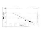
以下、表3に現像ローラの表層材料と水に対する接触角、画像カブリ不良の結果を示す。また、現像ローラ以外の構成を従来の現像装置のままとし、高温高湿環境(30℃、8
0%RH)に1日間放置した現像装置を用いてプリントアウト試験を行った結果を図3に示す。
Table 3 below shows the contact angle between the surface layer material of the developing roller and water, and the results of poor image fogging. Further, the configuration other than the developing roller is left as it is in the conventional developing device, and a high temperature and high humidity environment (30 ° C., 8 ° C.).
FIG. 3 shows the result of a printout test using a developing device left at 0% RH for 1 day.
図3から明らかなように、現像ローラ表面の水に対する接触角と画像カブリ不良との間には相関が見られた。つまり、現像ローラの表層材料を変化させ、現像ローラ表面の水に対する接触角を、100度以上とすることで、画像カブリ不良の発生を抑制することができた。 As is apparent from FIG. 3, there was a correlation between the contact angle of the developing roller surface with water and poor image fogging. That is, by changing the surface layer material of the developing roller and setting the contact angle of the developing roller surface with water to 100 degrees or more, it was possible to suppress the occurrence of image fogging failure.
なぜならば、現像ローラ表面の水に対する接触角を100度以上とすることによって、現像ローラ表面は、高温高湿環境下で表面及び内部に水分を含んだトナーを弾く性質を持つ。このため、トナーと現像ローラ表面の付着力は増加しない。トナーと現像ローラ表面の付着力の増加を防いだ結果、トナーと現像ローラ表面との摩擦機会が増加し、トナー層に付与される摩擦帯電量が増加する、と考えられる。このとき、トナー層に付与される摩擦帯電量は、現像ローラの表層材料の帯電系列等に依らず、水に対する接触角のみに依存していると考えられる。つまり、現像ローラ表層材料において、シリコーンとテフロン(登録商標)とは、帯電系列では正反対の傾向を示すはずであるが、2つの材料ともに接触角が高く、摩擦帯電量を増加させる傾向を持っていた。このため、トナー層に付与される摩擦帯電量は、水に対する接触角のみに依存していると考えられる。 This is because, by setting the contact angle of the surface of the developing roller to water to 100 degrees or more, the surface of the developing roller has a property of repelling toner containing moisture on the surface and inside in a high temperature and high humidity environment. For this reason, the adhesion force between the toner and the developing roller surface does not increase. As a result of preventing an increase in the adhesion between the toner and the surface of the developing roller, it is considered that the chance of friction between the toner and the surface of the developing roller increases, and the amount of triboelectric charge imparted to the toner layer increases. At this time, the amount of triboelectric charge imparted to the toner layer is considered to depend only on the contact angle with respect to water, regardless of the charging series of the surface layer material of the developing roller. That is, in the developing roller surface layer material, silicone and Teflon (registered trademark) should show the opposite tendency in the charging series, but both materials have a high contact angle and tend to increase the triboelectric charge amount. It was. For this reason, it is considered that the triboelectric charge applied to the toner layer depends only on the contact angle with water.
このように、トナーに付与された電荷が現像ブレードを通して放電された場合でも、摩擦機会の増加によってトナーに付与された摩擦帯電量が十分であるため、トナー層の摩擦帯電量の減少はない。 As described above, even when the charge applied to the toner is discharged through the developing blade, the amount of frictional charge applied to the toner due to the increase in the frictional opportunity is sufficient, and therefore the frictional charge amount of the toner layer does not decrease.
この結果、現像ブレードが導電性を有し、現像ブレードが電源又はアースに接続される場合でも、トナー層の摩擦帯電量は、環境変動の影響なく増加し画像カブリ不良の発生を抑制できる。 As a result, even when the developing blade has conductivity and the developing blade is connected to a power source or ground, the triboelectric charge amount of the toner layer increases without being affected by environmental fluctuations, and the occurrence of image fogging defects can be suppressed.
また、現像ローラ23の表面粗さの算術平均粗さ(Ra)を0.3μm以下とすることで、トナーと現像ローラ表面との摩擦機会を増加させることができ、トナー層の摩擦帯電量を増加させることができ、画像カブリ不良の発生を低減できる。
Further, by setting the arithmetic average roughness (Ra) of the surface roughness of the developing
また、現像ブレード25に直流バイアス電圧を印加し、現像ローラ23との間に電位差を設けることで、直流バイアス電圧によってトナー層に電荷を注入し、トナー層の摩擦帯電量を増加させることができ、画像カブリ不良の発生を低減できる。
Further, by applying a DC bias voltage to the developing
また、トナーを非磁性一成分現像剤とすることで、二成分現像剤と比べてキャリアを必要としないため、現像に際して、キャリアの劣化について特別な考慮を払う必要がない。 Further, since the toner is a non-magnetic one-component developer, a carrier is not required as compared with the two-component developer, so that it is not necessary to pay special consideration to carrier deterioration during development.
また、トナーを略球形とすることで、現像ブレード25とトナーの摩擦機会、現像ローラ23とトナーの摩擦機会、トナー同士の摩擦機会を増加させることができ、トナー層の摩擦帯電量を増加させることができ、画像カブリ不良の発生を低減できる。
Further, by making the toner substantially spherical, the chance of friction between the developing
以上説明したように、現像ブレード25が導電性を有し、現像ブレード25が電源又はアースに接続される場合でも、現像ローラ23の水に対する接触角を100度以上とすることで、現像ローラ表面に形成されたトナー層の摩擦帯電量を増加させることができる。
As described above, even when the developing
つまり、温度や湿度等の環境変化に伴って、トナー表面及び内部に含まれる水分量が増加した場合でも、トナーと現像ローラ表面とが水分を介して付着しない。トナーと現像ローラ表面との付着を防いだ結果、トナーと現像ローラ表面との摩擦機会が増加し、トナーに付与される摩擦帯電量が増加する。 That is, even when the amount of moisture contained in the toner surface and inside increases with environmental changes such as temperature and humidity, the toner and the developing roller surface do not adhere via moisture. As a result of preventing adhesion between the toner and the surface of the developing roller, the chance of friction between the toner and the surface of the developing roller increases, and the amount of frictional charge applied to the toner increases.
この結果、現像ブレード25が導電性を有する場合でも、トナーの摩擦帯電量を増加させることができ、画像カブリ不良の発生を低減することが可能となる。
As a result, even when the developing
このように、本実施例によれば、現像ローラ23上に形成されるトナー層の摩擦帯電量のばらつきを低減することができ、環境変化に対して影響の少ない略均一な画像特性及び高い信頼性を得ることが可能となる。
As described above, according to this embodiment, the variation in the triboelectric charge amount of the toner layer formed on the developing
図4は、本発明を適用したプロセスカートリッジ40の一例を示す概略断面図である。
FIG. 4 is a schematic sectional view showing an example of the
プロセスカートリッジ40は、現像装置44、感光ドラム45、帯電手段46、及び、クリーニング手段47で構成され、プラスチック製の現像枠体48,49により一体的にカートリッジ化される。ここで、現像装置44は、現像剤担持体としての現像ローラ41と、この現像ローラ41の外周面に面接触にて当接するように設けられた現像剤規制部材42、弾性ローラ43等で構成される。
The
即ち、本実施例のプロセスカートリッジ40は、上記実施例1で説明した現像装置14と、感光ドラム45に作用するプロセス構成部を一体的にユニット化したものである。従って、上述した全ての現像装置構成部が同様にプロセスカートリッジ40において適用されるものである。また、このプロセスカートリッジ40は画像形成装置に着脱可能に設けられるものである。本実施例においても、実施例1と同様の効果を得ることができる。
That is, the
14 現像装置
22 非磁性一成分トナー
23 現像ローラ
25 現像ブレード
14 Developing
Claims (8)
前記現像剤担持体に圧接するように設けられ、前記現像剤担持体に担持された前記現像剤の量を規制する現像剤規制部材と、
を備え、
前記現像剤規制部材が導電性を有し、前記現像剤規制部材が導通部に電気的に導通される現像装置において、
前記現像剤担持体は、前記現像剤担持体表面の水に対する接触角が100度以上となるように設けられていることを特徴とする現像装置。 A developer carrier for carrying and conveying the developer;
A developer regulating member that is provided in pressure contact with the developer carrying member and regulates the amount of the developer carried on the developer carrying member;
With
In the developing device in which the developer regulating member has electrical conductivity, and the developer regulating member is electrically conducted to the conducting portion.
The developing device, wherein the developer carrying member is provided so that a contact angle with respect to water of the surface of the developer carrying member is 100 degrees or more.
前記電圧印加手段により前記現像剤規制部材に直流バイアス電圧を印加して、前記現像剤担持体との間に電位差を設けることにより、前記現像剤担持体に担持された現像剤に電荷を付与し、前記現像剤の摩擦帯電量を増加させることを特徴とする請求項1又は2に記載の現像装置。 Voltage application means for applying a DC bias voltage to the developer regulating member;
By applying a DC bias voltage to the developer regulating member by the voltage applying means and providing a potential difference between the developer carrying member and the developer carrying member, a charge is imparted to the developer carried on the developer carrying member. The developing device according to claim 1, wherein the triboelectric charge amount of the developer is increased.
前記静電潜像担持体に現像作用を行う請求項1乃至5のいずれか1項に記載の現像装置と、
を備えることを特徴とする画像形成装置。 An electrostatic latent image carrier;
The developing device according to any one of claims 1 to 5, wherein a developing action is performed on the electrostatic latent image carrier.
An image forming apparatus comprising:
Priority Applications (1)
| Application Number | Priority Date | Filing Date | Title |
|---|---|---|---|
| JP2006342637A JP4914199B2 (en) | 2006-12-20 | 2006-12-20 | Developing device, process cartridge, and image forming apparatus |
Applications Claiming Priority (1)
| Application Number | Priority Date | Filing Date | Title |
|---|---|---|---|
| JP2006342637A JP4914199B2 (en) | 2006-12-20 | 2006-12-20 | Developing device, process cartridge, and image forming apparatus |
Publications (3)
| Publication Number | Publication Date |
|---|---|
| JP2008152192A true JP2008152192A (en) | 2008-07-03 |
| JP2008152192A5 JP2008152192A5 (en) | 2010-02-04 |
| JP4914199B2 JP4914199B2 (en) | 2012-04-11 |
Family
ID=39654380
Family Applications (1)
| Application Number | Title | Priority Date | Filing Date |
|---|---|---|---|
| JP2006342637A Active JP4914199B2 (en) | 2006-12-20 | 2006-12-20 | Developing device, process cartridge, and image forming apparatus |
Country Status (1)
| Country | Link |
|---|---|
| JP (1) | JP4914199B2 (en) |
Cited By (2)
| Publication number | Priority date | Publication date | Assignee | Title |
|---|---|---|---|---|
| JP2016024431A (en) * | 2014-07-24 | 2016-02-08 | 住友ゴム工業株式会社 | Semiconductor roller |
| JP7382004B2 (en) | 2019-11-29 | 2023-11-16 | 住友ゴム工業株式会社 | developing roller |
Citations (3)
| Publication number | Priority date | Publication date | Assignee | Title |
|---|---|---|---|---|
| JPH11282247A (en) * | 1998-03-30 | 1999-10-15 | Tokai Rubber Ind Ltd | Conductive elastic roll |
| JP2001083799A (en) * | 1999-09-14 | 2001-03-30 | Fuji Xerox Co Ltd | Developer layer regulation member, developing device using it and image forming device using it |
| JP2003057945A (en) * | 2001-08-13 | 2003-02-28 | Canon Inc | Developing device, process cartridge, and image forming apparatus |
-
2006
- 2006-12-20 JP JP2006342637A patent/JP4914199B2/en active Active
Patent Citations (3)
| Publication number | Priority date | Publication date | Assignee | Title |
|---|---|---|---|---|
| JPH11282247A (en) * | 1998-03-30 | 1999-10-15 | Tokai Rubber Ind Ltd | Conductive elastic roll |
| JP2001083799A (en) * | 1999-09-14 | 2001-03-30 | Fuji Xerox Co Ltd | Developer layer regulation member, developing device using it and image forming device using it |
| JP2003057945A (en) * | 2001-08-13 | 2003-02-28 | Canon Inc | Developing device, process cartridge, and image forming apparatus |
Cited By (2)
| Publication number | Priority date | Publication date | Assignee | Title |
|---|---|---|---|---|
| JP2016024431A (en) * | 2014-07-24 | 2016-02-08 | 住友ゴム工業株式会社 | Semiconductor roller |
| JP7382004B2 (en) | 2019-11-29 | 2023-11-16 | 住友ゴム工業株式会社 | developing roller |
Also Published As
| Publication number | Publication date |
|---|---|
| JP4914199B2 (en) | 2012-04-11 |
Similar Documents
| Publication | Publication Date | Title |
|---|---|---|
| JP4704081B2 (en) | Cleaning device, process unit, and image forming apparatus | |
| KR101813319B1 (en) | Developing apparatus, cartridge, and image forming apparatus | |
| US6341207B1 (en) | Cleanerless image forming method and system therefor | |
| JP2001265115A (en) | Developing machine and image forming apparatus | |
| JP2004012542A (en) | Developer regulating member, developing device, process cartridge and image forming apparatus | |
| JP4914199B2 (en) | Developing device, process cartridge, and image forming apparatus | |
| JP4731731B2 (en) | Developing device and image forming apparatus | |
| JPH0764389A (en) | Developing device | |
| KR101811101B1 (en) | Image forming apparatus | |
| JP2004037667A (en) | Developing roller, processing cartridge, and image forming apparatus | |
| JP2001242709A (en) | Developing device, cartridge and electrophotographic image forming device | |
| JP2006301479A (en) | Developing apparatus and image forming apparatus | |
| JP3782560B2 (en) | Developing device, process cartridge, and image forming apparatus | |
| JP2009042295A (en) | Cleaning device, process cartridge and image forming apparatus | |
| JP2001117366A (en) | Device and method for developing and electrophotographic image forming device | |
| JP2003057948A (en) | Image forming apparatus and process cartridge | |
| JP2003057945A (en) | Developing device, process cartridge, and image forming apparatus | |
| JP2005099340A (en) | Image forming apparatus | |
| JP6016601B2 (en) | Image forming apparatus and method for recovering electric resistance of developer regulating member | |
| JP2002258612A (en) | Developing device, process cartridge and image forming device | |
| JP2004133205A (en) | Developer control member, developing apparatus, process cartridge and image forming apparatus equipped with the developing apparatus | |
| JP2004157576A (en) | Developing roller, developing apparatus, process cartridge and image forming apparatus | |
| JP2010139681A (en) | Image forming apparatus and image forming method | |
| JP2000172138A (en) | Image forming device | |
| JP2009151084A (en) | Developing device and process cartridge |
Legal Events
| Date | Code | Title | Description |
|---|---|---|---|
| A521 | Written amendment |
Free format text: JAPANESE INTERMEDIATE CODE: A523 Effective date: 20091215 |
|
| A621 | Written request for application examination |
Free format text: JAPANESE INTERMEDIATE CODE: A621 Effective date: 20091215 |
|
| A977 | Report on retrieval |
Free format text: JAPANESE INTERMEDIATE CODE: A971007 Effective date: 20111006 |
|
| A131 | Notification of reasons for refusal |
Free format text: JAPANESE INTERMEDIATE CODE: A131 Effective date: 20111018 |
|
| A521 | Written amendment |
Free format text: JAPANESE INTERMEDIATE CODE: A523 Effective date: 20111219 |
|
| TRDD | Decision of grant or rejection written | ||
| A01 | Written decision to grant a patent or to grant a registration (utility model) |
Free format text: JAPANESE INTERMEDIATE CODE: A01 Effective date: 20120117 |
|
| A01 | Written decision to grant a patent or to grant a registration (utility model) |
Free format text: JAPANESE INTERMEDIATE CODE: A01 |
|
| A61 | First payment of annual fees (during grant procedure) |
Free format text: JAPANESE INTERMEDIATE CODE: A61 Effective date: 20120120 |
|
| R151 | Written notification of patent or utility model registration |
Ref document number: 4914199 Country of ref document: JP Free format text: JAPANESE INTERMEDIATE CODE: R151 |
|
| FPAY | Renewal fee payment (event date is renewal date of database) |
Free format text: PAYMENT UNTIL: 20150127 Year of fee payment: 3 |