JP2008109136A - Integrated method for removal halogen residues from substrate etched by thermal process - Google Patents
Integrated method for removal halogen residues from substrate etched by thermal process Download PDFInfo
- Publication number
- JP2008109136A JP2008109136A JP2007272802A JP2007272802A JP2008109136A JP 2008109136 A JP2008109136 A JP 2008109136A JP 2007272802 A JP2007272802 A JP 2007272802A JP 2007272802 A JP2007272802 A JP 2007272802A JP 2008109136 A JP2008109136 A JP 2008109136A
- Authority
- JP
- Japan
- Prior art keywords
- substrate
- processing
- chamber
- heating
- etched
- Prior art date
- Legal status (The legal status is an assumption and is not a legal conclusion. Google has not performed a legal analysis and makes no representation as to the accuracy of the status listed.)
- Pending
Links
Images


Classifications
-
- H—ELECTRICITY
- H01—ELECTRIC ELEMENTS
- H01L—SEMICONDUCTOR DEVICES NOT COVERED BY CLASS H10
- H01L21/00—Processes or apparatus adapted for the manufacture or treatment of semiconductor or solid state devices or of parts thereof
- H01L21/02—Manufacture or treatment of semiconductor devices or of parts thereof
- H01L21/02041—Cleaning
- H01L21/02057—Cleaning during device manufacture
- H01L21/02068—Cleaning during device manufacture during, before or after processing of conductive layers, e.g. polysilicon or amorphous silicon layers
- H01L21/02071—Cleaning during device manufacture during, before or after processing of conductive layers, e.g. polysilicon or amorphous silicon layers the processing being a delineation, e.g. RIE, of conductive layers
-
- H—ELECTRICITY
- H01—ELECTRIC ELEMENTS
- H01L—SEMICONDUCTOR DEVICES NOT COVERED BY CLASS H10
- H01L21/00—Processes or apparatus adapted for the manufacture or treatment of semiconductor or solid state devices or of parts thereof
- H01L21/02—Manufacture or treatment of semiconductor devices or of parts thereof
- H01L21/04—Manufacture or treatment of semiconductor devices or of parts thereof the devices having at least one potential-jump barrier or surface barrier, e.g. PN junction, depletion layer or carrier concentration layer
- H01L21/18—Manufacture or treatment of semiconductor devices or of parts thereof the devices having at least one potential-jump barrier or surface barrier, e.g. PN junction, depletion layer or carrier concentration layer the devices having semiconductor bodies comprising elements of Group IV of the Periodic System or AIIIBV compounds with or without impurities, e.g. doping materials
- H01L21/30—Treatment of semiconductor bodies using processes or apparatus not provided for in groups H01L21/20 - H01L21/26
- H01L21/302—Treatment of semiconductor bodies using processes or apparatus not provided for in groups H01L21/20 - H01L21/26 to change their surface-physical characteristics or shape, e.g. etching, polishing, cutting
- H01L21/304—Mechanical treatment, e.g. grinding, polishing, cutting
-
- H—ELECTRICITY
- H01—ELECTRIC ELEMENTS
- H01L—SEMICONDUCTOR DEVICES NOT COVERED BY CLASS H10
- H01L21/00—Processes or apparatus adapted for the manufacture or treatment of semiconductor or solid state devices or of parts thereof
- H01L21/02—Manufacture or treatment of semiconductor devices or of parts thereof
- H01L21/02041—Cleaning
- H01L21/02057—Cleaning during device manufacture
-
- H—ELECTRICITY
- H01—ELECTRIC ELEMENTS
- H01L—SEMICONDUCTOR DEVICES NOT COVERED BY CLASS H10
- H01L21/00—Processes or apparatus adapted for the manufacture or treatment of semiconductor or solid state devices or of parts thereof
- H01L21/67—Apparatus specially adapted for handling semiconductor or electric solid state devices during manufacture or treatment thereof; Apparatus specially adapted for handling wafers during manufacture or treatment of semiconductor or electric solid state devices or components ; Apparatus not specifically provided for elsewhere
- H01L21/67005—Apparatus not specifically provided for elsewhere
- H01L21/67011—Apparatus for manufacture or treatment
- H01L21/67098—Apparatus for thermal treatment
- H01L21/67115—Apparatus for thermal treatment mainly by radiation
-
- Y—GENERAL TAGGING OF NEW TECHNOLOGICAL DEVELOPMENTS; GENERAL TAGGING OF CROSS-SECTIONAL TECHNOLOGIES SPANNING OVER SEVERAL SECTIONS OF THE IPC; TECHNICAL SUBJECTS COVERED BY FORMER USPC CROSS-REFERENCE ART COLLECTIONS [XRACs] AND DIGESTS
- Y10—TECHNICAL SUBJECTS COVERED BY FORMER USPC
- Y10S—TECHNICAL SUBJECTS COVERED BY FORMER USPC CROSS-REFERENCE ART COLLECTIONS [XRACs] AND DIGESTS
- Y10S414/00—Material or article handling
- Y10S414/135—Associated with semiconductor wafer handling
-
- Y—GENERAL TAGGING OF NEW TECHNOLOGICAL DEVELOPMENTS; GENERAL TAGGING OF CROSS-SECTIONAL TECHNOLOGIES SPANNING OVER SEVERAL SECTIONS OF THE IPC; TECHNICAL SUBJECTS COVERED BY FORMER USPC CROSS-REFERENCE ART COLLECTIONS [XRACs] AND DIGESTS
- Y10—TECHNICAL SUBJECTS COVERED BY FORMER USPC
- Y10S—TECHNICAL SUBJECTS COVERED BY FORMER USPC CROSS-REFERENCE ART COLLECTIONS [XRACs] AND DIGESTS
- Y10S438/00—Semiconductor device manufacturing: process
- Y10S438/906—Cleaning of wafer as interim step
-
- Y—GENERAL TAGGING OF NEW TECHNOLOGICAL DEVELOPMENTS; GENERAL TAGGING OF CROSS-SECTIONAL TECHNOLOGIES SPANNING OVER SEVERAL SECTIONS OF THE IPC; TECHNICAL SUBJECTS COVERED BY FORMER USPC CROSS-REFERENCE ART COLLECTIONS [XRACs] AND DIGESTS
- Y10—TECHNICAL SUBJECTS COVERED BY FORMER USPC
- Y10S—TECHNICAL SUBJECTS COVERED BY FORMER USPC CROSS-REFERENCE ART COLLECTIONS [XRACs] AND DIGESTS
- Y10S438/00—Semiconductor device manufacturing: process
- Y10S438/963—Removing process residues from vertical substrate surfaces
Abstract
Description
発明の分野
[0001]本発明は、一般的に、半導体基板上にデバイスを製造するための方法及び装置に関する。より詳細には、本発明は、半導体基板上の層をプラズマエッチングした後、ハロゲン含有残渣を除去するための方法及び装置に関する。
Field of Invention
[0001] The present invention relates generally to methods and apparatus for manufacturing devices on a semiconductor substrate. More particularly, the present invention relates to a method and apparatus for removing halogen-containing residues after plasma etching a layer on a semiconductor substrate.
関連技術の説明
[0002]超大規模集積(ULSI)回路は、シリコン(Si)基板のような半導体基板上に形成され且つデバイス内の様々な機能を行うように協働する100万を超える電子デバイス(例えば、トランジスタ)を含むことができる。典型的には、ULSI回路に用いられるトランジスタは、相補形金属酸化膜半導体(CMOS)電界効果トランジスタである。CMOSトランジスタは、ポリシリコンゲート電極とゲート誘電体を備えるゲート構造を持ち、基板上に形成されるソース領域とドレイン領域の間に配置される。
Explanation of related technology
[0002] Ultra-large scale integrated (ULSI) circuits are formed on a semiconductor substrate, such as a silicon (Si) substrate, and more than one million electronic devices (eg, transistors) that cooperate to perform various functions within the device. ) Can be included. Typically, the transistors used in ULSI circuits are complementary metal oxide semiconductor (CMOS) field effect transistors. The CMOS transistor has a gate structure including a polysilicon gate electrode and a gate dielectric, and is disposed between a source region and a drain region formed on a substrate.
[0003]プラズマエッチングは、一般に、トランジスタと他の電子デバイスの製造に用いられる。トランジスタ構造を形成するために用いられるプラズマエッチングプロセスの間、積層膜の一つ以上の層(例えば、シリコン、ポリシリコン、二酸化ハフニウム(HfO2)、二酸化シリコン(SiO2)、金属材料等の層)は、典型的には、少なくとも一つのハロゲン含有ガス、例えば、臭化ハロゲン(HBr)、塩素(Cl2)、四フッ化炭素(CF4)等を含むエッチング剤にさらされる。このようなプロセスは、ハロゲン含有残渣を、基板上のエッチングされた特徴部、エッチングマスク等の表面に蓄積させる。 [0003] Plasma etching is commonly used in the manufacture of transistors and other electronic devices. During the plasma etching process used to form the transistor structure, one or more layers of the stack (eg, silicon, polysilicon, hafnium dioxide (HfO 2 ), silicon dioxide (SiO 2 ), metallic material, etc. ) Is typically exposed to an etchant comprising at least one halogen-containing gas, such as halogen bromide (HBr), chlorine (Cl 2 ), carbon tetrafluoride (CF 4 ), and the like. Such a process causes halogen-containing residues to accumulate on the surface of etched features, etch masks, etc. on the substrate.
[0004]非真空の環境(例えば、ファクトリインタフェース又は基板収納カセット内)及び/又は逐次処理の間にさらされているとき、ガス状のハロゲンやハロゲンベースの反応種(例えば、臭素(Br2)、塩素(Cl2)、塩化水素(HCl)等)は、エッチングの間に堆積されたハロゲン含有残渣から放出されてしまう。放出されたハロゲンやハロゲンベースの反応種は、パーティクル汚染を生じ、処理システムやファクトリインタフェースの内部の腐食だけでなく、基板上の金属層の露出部分の腐食を引き起こす。処理システムやファクトリインタフェースの洗浄や腐食したパーツの取替えは、時間を要し且つ費用のかかる手段である。 [0004] Gaseous halogens or halogen-based reactive species (eg, bromine (Br 2 )) when exposed to non-vacuum environments (eg, in a factory interface or substrate storage cassette) and / or during sequential processing , Chlorine (Cl 2 ), hydrogen chloride (HCl), etc.) are released from halogen-containing residues deposited during etching. The released halogen and halogen-based reactive species cause particle contamination, causing corrosion of the exposed portion of the metal layer on the substrate as well as internal corrosion of the processing system and factory interface. Cleaning the processing system and factory interface and replacing corroded parts is a time consuming and expensive means.
[0005]エッチングされた基板上のハロゲン含有残渣を取り除くためにいくつかのプロセスが開発されてきた。例えば、ハロゲン含有残渣をリアクタからアウトガスされポンプで送られることができる非腐食性揮発性化合物に変換するガス混合物にエッチングされた基板をさらすために、エッチングされた基板をリモートプラズマリアクタへ搬送することができる。しかしながら、このようなプロセスは、ツールの費用の増加、製造の生産性、処理能力の減少を引き起こし、高い製造原価をもたらす追加ステップと共に専用のプロセスチャンバを必要とする。 [0005] Several processes have been developed to remove halogen-containing residues on etched substrates. For example, transporting the etched substrate to a remote plasma reactor to expose the etched substrate to a gas mixture that converts the halogen-containing residue into a non-corrosive volatile compound that can be outgased from the reactor and pumped Can do. However, such a process results in increased tool costs, manufacturing productivity, decreased throughput, and requires a dedicated process chamber with additional steps that result in high manufacturing costs.
[0006]他の例において、ハロゲン含有残渣は、処理が更に望まれ、そのときに封入物が除去される時間までエッチングされた基板上に封入することができる。 [0006] In other examples, the halogen-containing residue can be encapsulated on the etched substrate until a time that further processing is desired and the encapsulant is then removed.
[0007]それ故、基板からハロゲン含有残渣を除去するための改良された方法及び装置が求められている。 [0007] Therefore, there is a need for an improved method and apparatus for removing halogen-containing residues from a substrate.
[0008]エッチングされた基板から揮発性残渣を除去する方法及びシステムが提供される。一実施形態において、基板から揮発性残渣を除去する方法は、真空気密プラットフォームを持つ処理システムを準備するステップと、プラットフォームのプロセスチャンバ内で基板をハロゲンを含む化学で処理するステップと、処理された基板をプラットフォーム内で処理して、処理された基板から揮発性残渣を放出させるステップとを含む。 [0008] Methods and systems are provided for removing volatile residues from an etched substrate. In one embodiment, a method for removing volatile residues from a substrate includes providing a processing system having a vacuum-tight platform, treating the substrate with a halogen-containing chemistry in a platform process chamber, Processing the substrate in the platform to release volatile residues from the processed substrate.
[0009]他の実施形態において、基板から揮発性残渣を除去する方法は、処理チャンバと処理チャンバの外部に配置された基板ヒータを持つ処理システムを準備するステップと、プロセスチャンバ内の基板をハロゲンを含む化学でエッチングするステップと、処理システム内の基板ヒータでエッチングされた基板を処理して基板から揮発性残渣を放出させるステップと、基板を加熱しつつ基板透過率変化を検出してプロセス終点を決定するステップとを含む。 [0009] In another embodiment, a method for removing volatile residues from a substrate includes providing a processing system having a processing chamber and a substrate heater disposed outside the processing chamber, and halogenating the substrate in the process chamber. Etching with a chemistry containing, processing the substrate etched with a substrate heater in a processing system to release volatile residues from the substrate, detecting changes in substrate transmittance while heating the substrate, and terminating the process Determining.
[0010]更に他の実施形態において、基板からハロゲン含有残渣を除去する方法は、少なくとも一つのプロセスチャンバと加熱素子を含むチャンバを持つ処理システムを準備するステップと、プロセスチャンバ内の基板を臭化物を含む化学でエッチングするステップと、加熱素子を含むプロセスチャンバ内でエッチングされた基板を処理するステップと、加熱の間、O3に基板をさらすステップとを含む。 [0010] In yet another embodiment, a method of removing a halogen-containing residue from a substrate includes providing a processing system having a chamber that includes at least one process chamber and a heating element, and removing bromide from the substrate in the process chamber. Etching with a containing chemistry, treating the etched substrate in a process chamber containing a heating element, and exposing the substrate to O 3 during heating.
[0011]本発明の上記特徴が詳しく理解され得るように、上で簡単にまとめられた本発明のより詳しい説明は実施形態によって参照することができ、その一部は添付の図面に示される。しかしながら、添付の図面は本発明の典型的な実施形態を示すだけであり、それ故、本発明の範囲を制限するものとみなされず、本発明は他の等しく有効な実施形態を許容することができる。 [0011] In order that the above features of the present invention may be more fully understood, a more detailed description of the invention briefly summarized above may be referred to by embodiments, some of which are illustrated in the accompanying drawings. However, the attached drawings only show exemplary embodiments of the invention and are therefore not considered to limit the scope of the invention, and the invention may allow other equally effective embodiments. it can.
[0016]理解を容易にするために、同一の符号は、可能な場合、図に共通する同一の要素を示すために用いられている。一実施形態の要素と特徴は、更に詳述せずに他の実施形態に有益に組込まれてもよいと考えられる。 [0016] To facilitate understanding, identical reference numerals have been used, where possible, to designate identical elements that are common to the figures. It is contemplated that elements and features of one embodiment may be beneficially incorporated into other embodiments without further elaboration.
[0017]しかしながら、添付の図面は、本発明の例示的な実施形態だけを示し、それ故、その範囲を制限するとみなされず、発明は他の等しく有効な実施形態を許容することができることは留意すべきである。
詳細な説明
[0018]本発明は、前処理又は後処理専用にすることができる別個のチャンバに入れることなく主エッチングチャンバと基板運搬FOUPの間のエンルートを基板ウエハが通過するいずれかの位置で前処理及び又は後処理(主プロセスチャンバの外部)するための方法及びシステムを提供する。基板が通過する位置は、ロードロックチャンバと搬送チャンバを含み、それらに限定されない。更に、本発明は、ハロゲンを含むエッチング剤を用いてエッチングされる基板からハロゲン含有残渣を除去するようなエンルート後処理のための方法及びシステムを提供する。ハロゲン含有残渣除去プロセスは、システム内の真空プラットフォームの下のいずれかの位置で行ってもよいと考えられる。一実施形態において、基板エッチングの間に堆積されたハロゲン含有残渣は、処理システムの真空気密プラットフォーム内で熱処理によって除去される。熱処理に利用することができる真空気密プラットフォームの部分は、ロボットブレード上に、ロードロックチャンバ、搬送チャンバ、処理チャンバ、また、主エッチングチャンバとウエハ運搬FOUPの間の処理システムの真空中の他のいずれかの適当な位置とを含んでいる。熱プロセスは、エッチングされた基板を加熱し、ハロゲン含有残渣をポンプで送り出すことができる非揮発性化合物へ変換させる。ハロゲン含有残渣除去プロセスを行うのに選ばれる位置は、全体のプロセスサイクル時間が不利に影響しないような“エンルート”を選ぶことができる。発明は、実質的に、高生産性とプロセス処理能力を維持しつつ、処理システムと基板の環境を汚染と腐食から防止する。
[0017] However, it is noted that the accompanying drawings show only exemplary embodiments of the invention and are therefore not considered to limit its scope, and the invention may allow other equally valid embodiments. Should.
Detailed description
[0018] The present invention provides for pre-processing and processing at any location where the substrate wafer passes through the enroute between the main etch chamber and the substrate transport FOUP without entering a separate chamber that can be dedicated to pre-processing or post-processing. Alternatively, methods and systems for post processing (outside of the main process chamber) are provided. The position through which the substrate passes includes, but is not limited to, a load lock chamber and a transfer chamber. Furthermore, the present invention provides a method and system for post-enroute processing that removes halogen-containing residues from a substrate that is etched using a halogen-containing etchant. It is contemplated that the halogen-containing residue removal process may be performed at any location below the vacuum platform in the system. In one embodiment, halogen-containing residues deposited during substrate etching are removed by heat treatment within a vacuum tight platform of the processing system. The portion of the vacuum-tight platform that can be used for heat treatment is on the robot blade, any of the load lock chamber, transfer chamber, processing chamber, and any other in the vacuum of the processing system between the main etch chamber and wafer transfer FOUP. And appropriate locations. The thermal process heats the etched substrate and converts the halogen-containing residue into a non-volatile compound that can be pumped out. The position chosen to perform the halogen-containing residue removal process can be selected as an “enroute” so that the overall process cycle time is not adversely affected. The invention substantially prevents the processing system and substrate environment from contamination and corrosion while maintaining high productivity and process throughput.
[0019]図1は、ハロゲン含有残渣を除去するための熱プロセスを行うことができる処理システム100の一実施形態の平面概略図である。一実施形態において、処理システム100は、カリフォルニア、サンタクララにあるアプライドマテリアルズ社から市販されている適切に適合されたCENTURA(登録商標)総合処理システムであるのがよい。他の処理システム(他の製造業者からのものを含む)は、発明から利益を得るように適合されているのがよい。
[0019] FIG. 1 is a schematic plan view of one embodiment of a
[0020]システム100は、真空気密処理プラットフォーム104と、ファクトリインタフェース102と、システムコントローラ144とを含む。プラットフォーム104は、処理チャンバ110、112、132、128、120として示される複数の処理チャンバと、真空基板搬送チャンバ136に結合される少なくとも一つのロードロックチャンバ122とを含む。二つのロードロックチャンバ122は、図1に示されている。ファクトリインタフェース102は、ロードロックチャンバ122によって搬送チャンバ136に結合される。
[0020] The
[0021]一実施形態において、ファクトリインタフェース102は、少なくとも一つのドッキングステーション108と基板の搬送を容易にする少なくとも一つのファクトリインタフェースロボット114を備えている。ドッキングステーション108は、一つ以上の前開口部付きポッド(FOUP)を受け入れるように構成される。二つのFOUPS106A-Bは、図1の実施形態に示されている。ロボット114の一端に配置されたブレード116を持つファクトリインタフェースロボット114は、基板をファクトリインタフェース102から処理プラットフォーム104のロードロックチャンバ122に搬送するように構成される。必要により、一つ以上の計測ステーション118は、ファクトリインタフェース102内にある間基板の計測を容易にするためにファクトリインタフェース102のターミナル126に結合されていてもよい。
[0021] In one embodiment, the
[0022]各ロードロックチャンバ122は、ファクトリインタフェース102に結合された第一ポートと搬送チャンバ136に結合された第二ポートを持つ。ロードロックチャンバ122は、搬送チャンバ136の真空環境とファクトリインタフェース102の実質的な周囲(例えば、大気)環境の間を基板が通過することを容易にするためにロードロックチャンバ122にポンプで送り通気する圧力制御システム(図示せず)に結合される。
Each
[0023]搬送チャンバ136は、その中に配置された真空ロボット130を持つ。真空ロボット130は、基板124をロードロックチャンバ122とプロセスチャンバ110、112、132、128、120の間に搬送することができるブレード134を持つ。
[0023] The
[0024]一実施形態において、少なくとも一つのプロセスチャンバ110,112、132、128、120は、エッチングチャンバである。例えば、エッチングチャンバは、アプライドマテリアルズ社から入手できる分離プラズマソース(DPS)チャンバであるのがよい。DPSエッチングチャンバは、高密度プラズマを生成するために誘導ソースを用い、基板をバイアスするために高周波(RF)電源を備えている。或いは、プロセスチャンバ110,112、132、128、120の少なくとも一つは、アプライドマテリアルズ社から入手できるHARTTM,E-MAX(登録商標)、DPS(登録商標)、DPSII、PRODUCERE、又はENABLER(登録商標)エッチングチャンバの一つ、又は他の製造業者からのものを含む他のチャンバであるのがよい。エッチングチャンバ、例えば、チャンバ110は、その中に配置された基板124をエッチングするためにハロゲン含有ガスを用いることができる。ハロゲン含有ガスの例としては、臭化水素(HBr)、塩素(Cl2)、四フッ化炭素(CF4)等が挙げられる。基板124をエッチングした後、ハロゲン含有残渣は基板表面上に残されてもよい。ハロゲン含有残渣は、ここに記載された熱プロセスによって除去することができる。熱プロセスは、インサイチュプラットフォーム104で、例えば、基板を加熱するために取り付けられる処理チャンバ110、112、132、128、120の一つで行われる。熱プロセスが行われるプラットフォーム104の領域は、エネルギーゼネレータと、基板温度をモニタするように、熱プロセスの間、基板をモニタするように配置されたセンサを含むことができる。例示的実施形態において、熱処理プロセスは、ロードロックチャンバ122内で行われるが、熱処理プロセスは、システム100の適切に取り付けられた領域内で行うことができる。
[0024] In one embodiment, at least one
[0025]システムコントローラ144は、プロセスシステム100に結合される。システムコントローラ144は、システム100のプロセスチャンバ110、112、132、128、120の直接制御を用いて、或いはプロセスチャンバ110、112、132、128、120とシステム100と関連するコンピュータ(又はコントローラ)を制御することによってシステム100の動作を制御する。動作中、システムコントローラ144は、データ収集と、システム100の性能を最適化する各チャンバとシステムコントローラ144からのフィードバックを可能にする。
[0025] The
[0026]システムコントローラ144は、一般的に、中央処理装置(CPU)138と、メモリ140と、支援回路142とを含む。CPU138は、工業環境で使用し得る汎用コンピュータプロセッサのいずれかの形の一つであってもよい。支援回路142は、慣用的にCPU138に結合され、キャッシュメモリ、クロック回路、入力/出力サブシステム、電源等を備えることができる。図4によって後述されるハロゲン含有残渣を除去するための方法のようなソフトウエアルーチンは、CPU138によって実行されるとき、CPU138を個々の目的のコンピュータ(コントローラ)144へ変換する。ソフトウエアルーチンは、システム100から離れて位置する第二コントローラ(図示せず)によって記憶及び/又は実行することができる。
[0026] The
[0027]図2は、基板上に熱プロセスを行うために用いることができるロードロックチャンバ122を示す一実施形態である。ロードロックチャンバ122は、一般的に、チャンバ本体202と、第一基板ホルダ204と、第二基板ホルダ206と、温度制御ペデスタル240と、エネルギー源、例えば、ヒータモジュール270とを含む。センサ298は、温度コントローラペデスタル240内に配置される。チャンバ本体202は、アルミニウムのような材料の唯一の本体から製造することができる。チャンバ本体202は、チャンバ容積218を画成する、第一側壁208と、第二側壁210と、最上部214と、底部216とを含む。典型的には石英から構成される窓250は、チャンバ本体の最上部214内に配置され、ヒータモジュール270によって少なくとも部分的に覆われている。一実施形態において、複数のランプ294は、基板熱処理のために熱を生成するためにヒータモジュール270内に配置されている。一実施形態において、ランプ294は、約700nm〜約14000nmの波長を持つ赤外線を供給する石英ハロゲンランプである。ランプ294から生成される赤外線は、基板に熱を供給するとともに約500℃まで基板温度を上げる。一般的に、センサ298の波長は、測定によって、例えば、熱プロセス終点の温度が探究される温度範囲に加熱される材料及び/又は膜を通る透過率変化が大きいように選択される。
[0027] FIG. 2 is one embodiment showing a
[0028]一実施形態において、センサ298は、約100℃〜約500℃の基板温度範囲を測定するように適合されたInGaAsダイオードセンサである。センサ298は、必要により、光コリメータ292とフィルタ278と光学的に整列している。光コリメータは、光コンジット276(即ち、光ファイバ)の端部274と基板296の間のペデスタル240に配置される。光コンジット276は、フィルタ278まで基板296とコリメータ292を通って通過する収集エネルギーを検出する。フィルタ278は、光コリメータから収集された信号をフィルタにかけるように適合され、所望の波長を持つIR光のみをセンサ298に供給する。
[0028] In one embodiment,
[0029]一実施形態において、光コリメータ292は、散乱したエネルギーと他のノイズのコンジット276への入力を最小にするように選択される所定の角度290で、基板に入射するエネルギーが光コンジット276に入ることを許容するように選択されるアパーチャを持つ。例えば、光コリメータ292の選択された角度290は、光288が集められる角度290によって定義される円錐内の基板だけを通過することを可能にし、選択された角度290の外の角度で基板に入射する光が光コンジット250へ入ることを防止する。チャンバ壁284からの望まない反射光及び/又はバックグラウンド282、280から生成されたノイズは、コリメータ292を通って光コンジット270に入る信号を妨害すること、また、最終的にフィルタ278を通ってセンサ298に達することを防止する。センサ298に達する光エネルギーは、その後更に、基板298の温度を計算するために解析される。
[0029] In one embodiment, the
[0030]チャンバ容積218の圧力は、ロードロックチャンバ122が、搬送チャンバの環境と実質的に適合するように排気させることができ且つファクトリインタフェース102の環境と実質的に適合するように通気させることができるように制御することができる。チャンバ本体202は、微粒子の汚染を最小にするために、通気と排気の間、チャンバ容積218内に層流を与える一つ以上のベント通路230とポンプ通路232を含む。ベント通路230は、更に、ガス混合物をチャンバ容積218へ供給するためにガス源252に結合することができる。ガス源から供給することができるガスの例としては、窒素(N2)、アルゴン(Ar)、水素(H2)、アルカン、アルケン、ヘリウム(He)、酸素(O2)、オゾン(O3)、水蒸気(H2O)等が挙げられる。ポンプ通路232は、ガスをポンプで送るとともにロードロックチャンバ122の圧力を所望の点で制御するためにポンプ236に結合される。
[0030] The pressure in the
[0031]第一装填ポート238は、基板124がロードロックチャンバ122とファクトリインタフェース102の間に搬送されることを可能にするようにチャンバ本体202の第一壁208に配置される。第一スリットバルブ244は、ファクトリインタフェース102からロードロックチャンバ122を分離するために第一装填ポート238を選択的にシールする。第二装填ポート239は、基板124がロードロックチャンバ122と搬送チャンバ136の間に搬送されることを可能にするために、チャンバ本体202の第二壁210に配置される。第一スリットバルブ244とほとんど同様の第二スリットバルブ246は、搬送チャンバ136の真空環境からロードロックチャンバ122を分離するように第二ローディングポート239を選択的にシールする。
[0031] The
[0032]第一基板ホルダ204は、チャンバ底部216の上に配置された第二基板ホルダ206に同軸上に結合される(即ち、最上部に積み重ねられる)。基板ホルダ204、206は、一般的に、チャンバ本体202の底部216を通って伸びるシャフト258に結合されるフープ220に取り付けられる。各基板ホルダ204、206は一基板を保持するように構成される。シャフト258は、チャンバ本体202内で基板ホルダ204と206の上昇を制御するロードロックチャンバ122の外部に配置されたリフトメカニズム260に結合される。第一基板ホルダ204はファクトリインタフェース102からの処理されていない基板を保つために利用され、第二基板ホルダ206は搬送チャンバ136から戻る処理された基板を保つために利用される。図2に示された実施形態において、処理された基板296は、処理チャンバ110、112、132、128、120のいずれか一つで処理した後、第二基板ホルダ206上に位置する。
[0032] The
[0033]図3は、図1の処理システム100の搬送チャンバ136を示す部分断面図である。図3に示された一実施形態において、搬送チャンバ136は、揮発性残渣が基板から放出できるように基板を熱処理するように構成される。搬送チャンバに配置された基板は、適切ないずれのヒータ又はエネルギー源によっても加熱することができる。一例において、基板は、搬送チャンバロボット130のブレード134に内蔵された抵抗加熱素子322によって加熱することができる。他の実施形態において、基板は、搬送チャンバ136の最上部の中に、上に、又は搬送チャンバ136の下に配置されるヒータモジュール302によって加熱することができる。ヒータモジュール302は、基板を加熱するのに適した一つ以上のランプ306を含んでもよい。更に他の実施形態において、基板は、搬送チャンバ136に配置された加熱されたペデスタル314によって加熱することができる。ペデスタル314は、抵抗ヒータ322又は他の適切な加熱デバイスを含むことができる。基板は、真空中である搬送チャンバ136又はシステム100の他の部分内部の他の方法によって加熱してもよいと考えられる。
[0033] FIG. 3 is a partial cross-sectional view illustrating the
[0034]基板の加熱中、基板は、基板からの揮発物質の放出と、システムから放出された揮発物質の除去を容易にする一つ以上のガスにさらすことができる。図3に示される実施形態において、搬送チャンバ136は、異なるプロセスガスをガス源316から搬送チャンバ136の内部容積330に供給するように適合されるガス通路318を含む。ガス源316から供給することができるガスの例としては、窒素(N2)、アルゴン(Ar)、水素(H2)、アルカン、アルケン、ヘリウム(He)、酸素(O2)、オゾン(O3)、水蒸気(H2O)等が挙げられる。
[0034] During heating of the substrate, the substrate may be exposed to one or more gases that facilitate release of volatiles from the substrate and removal of volatiles released from the system. In the embodiment shown in FIG. 3, the
[0035]必要により、搬送チャンバ136は、加熱の間、基板の温度を感知するように取り付けることができる。一実施形態において、エネルギーゼネレータ304は、基板296を通ってセンサ310へ透過されるエネルギー信号を与える搬送チャンバ136の最上部に配置される。エネルギーゼネレータ304は、レーザ、広いビーム光源又は他の適切な波発生器であってもよく、一実施形態において、ゼネレータ304は、ランプ306の一つであってもよい。
[0035] If desired, the
[0036]コリメータ312は、ゼネレータ304から基板296を通る所定の入射角度内で透過されたエネルギーを収集するために基板296の下に配置することができる。基板296を透過し且つコリメータによって収集されたエネルギーは、続いて、図2に関して上述したように基板の温度を決定するための光ファイバコンジットによってセンサ310に透過される。
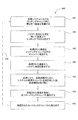
[0036] The
[0037]図4は、本発明に従って基板からハロゲン含有残渣を除去する方法400を示す流れ図である。方法400は、図1の処理装置100で行われる。方法400は、他の製造業者からのものを含む他の適切な処理システムで行うことができると考えられる。
[0037] FIG. 4 is a flow diagram illustrating a
[0038]方法400は、ステップ402で、エッチングプロセスを行う処理システム100内でエッチングチャンバ、例えば、エッチングチャンバ110、112、132、128、120の一つに配置された層を持つ基板を準備することによって開始する。ファクトリインタフェースロボット114は、処理すべき基板をFOUP106A-Bの一つからロードロックチャンバ122内の第一基板ホルダ204へ搬送する。基板は、膜処理が行われるいずれの基板又は材料の表面であってもよい。一実施形態において、基板は層又はゲート構造のような構造を形成するように使われるその上に形成される一つ以上の層であってもよい。或いは、基板は、特徴部又は構造の基板への搬送を容易するために基板上に配置されたエッチングマスク及び/又はエッチング停止層としてのマスク層を使う。他の実施形態において、基板は多層膜を、例えば、デュアルダマシン構造等の異なるパターン及び/又は特徴部を形成するために使われる積層膜を持つのがよい。基板は、結晶シリコン(例えばSi<100>又はSi<111>)、酸化シリコン、ストレインドシリコン、シリコンゲルマニウム、ドープされた又はドープされていない多結晶シリコン、ドープされた又はドープされていない、また、パターン形成された又はパターン形成されていないウエハの絶縁体上のシリコン(SOI)、炭素ドープされた酸化シリコン、窒化シリコン、ドープされたシリコン、ゲルマニウム、ガリウムヒ素、ガラス、サファイア、シリコン上に配置された金属層等であってもよい。基板は、200mm又は300mm径ウエハのような様々な寸法だけでなく、矩形又は正方形のパネルを有してもよい。本発明に示される実施形態において、基板はシリコン半導体基板であるのがよい。
[0038] The
[0039]一実施形態において、ロードロックチャンバ122に搬送された基板は、ロードロックチャンバ122内のヒータモジュール270又は温度制御されたペデスタル240によって所定の温度に予熱されるのがよい。他の実施形態において、基板は搬送チャンバロボット130のブレード中に予熱される。一実施形態において、基板は、約20℃〜約400℃の温度に予熱されるのがよい。ロードロックチャンバ122と搬送チャンバ136内の圧力がほぼ同じになった後、真空ロボット130は、基板を処理チャンバの一つ、例えば、チャンバ110に搬送する。
[0039] In one embodiment, the substrate transferred to the
[0040]ステップ404において、基板を処理チャンバ110内でエッチングして、基板上に所望の特徴部とパターンを形成する。基板が基板表面上に配置されたマスク層を持つ実施形態において、エッチングプロセスは所望の特徴部やパターンを形成しつつ同時にマスク層をエッチングする。
[0040] In
[0041]一実施形態において、基板は少なくともハロゲン含有ガスを持つガス混合物によってエッチングされる。ハロゲン含有ガスの適切な例としては、臭化水素(HBr)、塩素(Cl2)、四フッ化炭素(CF4)が挙げられるが、これらに限定されない。多結晶シリコンをエッチングするのに適切な例示的実施形態において、プロセスチャンバ110に供給されるガス混合物は、約20sccm〜約300sccm、例えば、約20sccm〜約60sccm、例えば、約40sccmの流量で臭化水素(HBr)と塩素(Cl2)ガスを含むガス混合物を供給する。不活性ガスは、ガス混合物と共に処理チャンバ110に供給されてもよい。不活性ガスの適切な例としては、窒素(N2)、アルゴン(Ar)、ヘリウム(He)等を挙げることができる。一実施形態において、N2のような不活性ガスは、約0sccm〜約200sccm、例えば、約0sccm〜約40sccm、例えば、約20sccmの流量でガス混合物と共に供給するのがよい。一酸化炭素(CO)のような還元ガスをガス混合物と共に供給してもよい。エッチングプロセスのためのプラズマ電力は約200ワット〜約3000ワット、例えば、約500ワット〜約1500ワット、例えば、約1100ワットに維持されるのがよく、バイアス電力は約0ワット〜約300ワット、例えば、約0ワット〜約80ワット、例えば、約20ワットに維持されるのがよい。プロセス圧力は約2ミリトール〜約100ミリトール、例えば、約2ミリトール〜約20ミリトール、例えば約4ミリトールで制御することができ、基板温度は約0℃〜約200℃、例えば、約0℃〜約100℃、例えば、約45℃に維持することができる。
[0041] In one embodiment, the substrate is etched with a gas mixture having at least a halogen-containing gas. Suitable examples of halogen-containing gases include, but are not limited to, hydrogen bromide (HBr), chlorine (Cl 2 ), carbon tetrafluoride (CF 4 ). In an exemplary embodiment suitable for etching polycrystalline silicon, the gas mixture supplied to the
[0042]エッチングプロセスの間、エッチングされた物質は、エッチング剤化学の成分だけでなく、マスク層の成分、また、エッチングプロセスの副生成物と組合わせることができ、それによりハロゲン含有残渣が形成される。一実施形態において、エッチングすべき基板上の物質としては、フォトレジスト層、ハードマスク層、ボトム無反射コーティング(BARC)、多結晶シリコン、結晶シリコン、ゲート酸化物、金属ゲート、例えば、窒化チタン(TiN)、及び高k物質、例えば、酸化アルミニウム(Al2O3)、ハフニウム含有酸化物を挙げることができる。ハードマスク層の適切な例としては、窒化シリコン、TEOS、酸化シリコン、アモルファスカーボン及び炭化シリコンが挙げられる。ハロゲン含有残渣は、基板の表面上に堆積される。大気圧及び/又は水蒸気にさらされた場合には、ハロゲン含有残渣は、ガス反応種、例えば、臭素(Br2)、塩素(Cl2)、塩化水素(HCl)、臭化水素(HBr)等を放出(例えば、アウトガス)することができる。このような反応種の放出は、基板搬送の間に処理装置とファクトリインタフェース、例えば、図1に記載された真空気密処理プラットフォーム104とファクトリインタフェース102の腐食やパーティクルの汚染を引き起こすことができる。Cu、Al、Wのような金属層が基板表面にさらされる実施形態において、下記の本発明のプロセスによって除去されない場合には、放出されたガス反応種によって金属層が腐食されてしまい、そのことにより、基板上に形成されたデバイスの性能が逆に劣化する。
[0042] During the etching process, the etched material can be combined not only with the components of the etchant chemistry, but also with the components of the mask layer and by-products of the etching process, thereby forming a halogen-containing residue. Is done. In one embodiment, the material on the substrate to be etched includes a photoresist layer, a hard mask layer, a bottom anti-reflective coating (BARC), polycrystalline silicon, crystalline silicon, a gate oxide, a metal gate, such as titanium nitride ( TiN), and high-k materials such as aluminum oxide (Al 2 O 3 ), hafnium-containing oxides. Suitable examples of hard mask layers include silicon nitride, TEOS, silicon oxide, amorphous carbon, and silicon carbide. A halogen-containing residue is deposited on the surface of the substrate. When exposed to atmospheric pressure and / or water vapor, the halogen-containing residue can be a gas reactive species such as bromine (Br 2 ), chlorine (Cl 2 ), hydrogen chloride (HCl), hydrogen bromide (HBr), etc. Can be released (eg, outgassed). Such release of reactive species can cause corrosion and particle contamination of the processing equipment and factory interface, eg, the vacuum-
[0043]ハロゲンもまた、エッチング以外の方法で真空環境で処理される基板の表面上に存在することができる。それ故、ハロゲンは、下記の本方法の適用可能な部分を用いてそれらの基板から除去することができると考えられる。 [0043] Halogen can also be present on the surface of a substrate that is processed in a vacuum environment by methods other than etching. Therefore, it is believed that halogens can be removed from their substrates using the applicable part of the method below.
[0044]ステップ406において、処理(例えば、エッチング)された基板は、プロセスの完了後、エッチング処理チャンバ110から取り出される。処理(例えば、エッチング)された基板は、続いて、更に下記の熱プロセスを行うために、エッチングプロセスを行うエッチングチャンバ以外の処理システム100のいずれかのチャンバに搬送することができる。例えば、エッチングされたまま、続いて、その他の処理チャンバ112、132、128、120のいずれか一つ、搬送チャンバ136、ロードロックチャンバ122又はプラットフォーム104内の他のパーツを含む熱チャンバに搬送されてもよく、ここで、基板はハロゲンを放出するように加熱されてもよい。必要により、熱プロセスは、ファクトリインタフェース102、計測ステーション118に存在してもよい。処理(例えば、エッチング)された基板は、FOUP106A-B又は他の位置で大気状態又は水蒸気へさらす前のステップ404の間に生成された基板からハロゲン含有残渣を除去するためにステップ408で熱的に処理される。ステップ406は省略されてもよく、下記の熱プロセスステップ408は、基板がエッチング或いは別の方法でハロゲンにさらされるチャンバ内で行われてもよく、又はステップ408はロードロックチャンバ又は他の適切な位置で行われてもいと考えられる。また、上記熱プロセスステップ406がエッチングされた基板からハロゲンを効果的に除去する場合には、ステップ408は省略されてもよいと考えられる。
[0044] In
[0045]ステップ408において、基板を熱的に処理して、基板からハロゲン及び/又はハロゲン含有残渣を除去する。一実施形態において、ステップ408は、基板が加熱素子を持つロボット114、130の一つに配置されるか又は揮発物質を放出する温度に基板を加熱するのに適切なヒータに十分密接して基板を位置させるように構成される間に行われるのがよい。例えば、チャンバ間に基板を搬送する順序の間、基板が搬送ロボット130上に配置される間にステップ408の熱処理プロセスが行われるのがよい。或いは、熱プロセスが行われる間、ステップ408の基板は基板支持デバイス内に位置させてもよい。一実施形態において、ステップ408の熱プロセスは、ロードロックチャンバ122又は搬送チャンバ136の同様に構成された領域又は処理チャンバ112、132、128、120の一つで行われるのがよい。下の例示的な説明において、ステップ408は、ロードロックチャンバ122内で行われるように記載される。加熱ステップと必要によりガスエンクロージャと感知するステップの少なくとも一つは、プラットフォーム104又はファクトリインタフェース102の適切に取り付けられた他の領域で行うことができると考えられる。
[0045] In
[0046]ステップ408の例示的な実施形態において、熱処理プロセスは、エッチングされた基板表面からハロゲン含有残渣を除去するためにロードロックチャンバ122内で行われる。第二基板ホルダ206によって固定されたエッチングされた基板は、基板124をヒータモジュール270へ向かって上昇させ、それにより基板に対する熱搬送強度が増加する。ヒータモジュール270からの加熱は、基板の表面の温度を上昇させ、それによりエッチングされた基板表面に配置されたハロゲンベースの反応種が放出及び/又はアウトガスする。基板温度が上昇するにつれて、シリコン基板の光エネルギー吸収挙動が同様に変化する。例えば、加熱モジュール270からの光がシリコン基板を加熱し基板温度を上昇させるにつれて、高基板温度でシリコン材料の光エネルギー吸収が高いために基板による光エネルギーの吸収が増加する。従って、加熱につれてシリコン基板を通る光が透過しなくなる。センサ298による基板透過率変化を測定することによって、基板温度が計算され、熱処理プロセスの間の基板温度を制御するプロセス終点が決定され得る。
[0046] In the exemplary embodiment of
[0047]一実施形態において、ヒータモジュール270は、基板を約20℃〜約500℃、例えば、約150℃〜約400℃、例えば、約300℃の温度に約5秒〜約120秒、例えば、約20秒で加熱する。ヒータモジュール270による基板の急速な加熱は、プロセスサイクル時間を増さずにエッチングされた基板上のハロゲン含有残渣が除去されることを可能にする。一実施形態において、エッチングされた基板上のハロゲン含有残渣がそこから除去されるまで、基板はヒータモジュール270によって所定の時間加熱されるのがよい。或いは、終点は、基板温度をモニタすること、例えば、基板を通る光透過率変化をモニタすることによって検出することができる。
[0047] In one embodiment, the
[0048]一実施形態において、エッチングされた基板を加熱しつつガス源252からロードロックチャンバ122にガス混合物を供給することができる。エッチングされた基板は、ガス混合物にさらされ反応する。ガス混合物はアウトガスされたハロゲンベースの反応種をロードロックチャンバ122からポンプで送られる非腐食性揮発性化合物に変換させる。ガス混合物としては、酸素含有ガス、例えば、O2、O3、水蒸気(H2O)、水素含有ガス、例えば、H2、フォーミングガス、水蒸気(H2O)、アルカン、アルケン等、又は不活性ガス、例えば、窒素ガス(N2)、アルゴン(Ar)、ヘリウム(He)等を挙げることができる。例えば、ガス混合物としては、酸素、窒素、及び水素含有ガスを挙げることができる。一実施形態において、水素含有ガスは、水素(H2)及び水蒸気(H2O)の少なくとも一つである。他の例において、ガス混合物としてはオゾンガス(O3)を挙げることができる。基板上にマスク層がある実施形態において、マスク層はハロゲン含有残渣と同時に除去することができる。例えば、マスクはロードロックチャンバ内でフォトレジストから除去される。
[0048] In one embodiment, a gas mixture may be supplied from the gas source 252 to the
[0049]一実施形態において、ガス混合物は、約100sccm〜約10,000sccm、例えば、約7000sccmの流量で供給されるのがよい。ハロゲン含有残渣が臭素ベースのエッチングの化学の使用から得られるほとんど臭素ベースの残渣である実施形態において、ガス混合物としては、オゾンガス(O3/O2)及び/又は他の不活性ガス、例えば、O2やN2を挙げることができる。オゾンガス(O3/O2)は、約100sccm〜約10,000sccm、例えば、約7000sccmの流量で供給されるのがよい。或いは、不活性ガスは、約100sccm〜約10,000sccm、例えば、約500sccmの流量でオゾンガス(O3/O2)と供給することができる。残留ガスアナライザ(RGA)は、エッチングされた基板表面上に残存するハロゲン含有残渣を検出するために使うことができる。 [0049] In one embodiment, the gas mixture may be provided at a flow rate between about 100 seem and about 10,000 seem, for example about 7000 seem. In embodiments where the halogen-containing residue is an almost bromine-based residue obtained from the use of bromine-based etching chemistry, the gas mixture may include ozone gas (O 3 / O 2 ) and / or other inert gases, such as O 2 and N 2 can be mentioned. Ozone gas (O 3 / O 2 ) may be supplied at a flow rate between about 100 sccm and about 10,000 sccm, for example, about 7000 sccm. Alternatively, the inert gas can be supplied with ozone gas (O 3 / O 2 ) at a flow rate between about 100 sccm and about 10,000 sccm, for example, about 500 sccm. A residual gas analyzer (RGA) can be used to detect halogen-containing residues remaining on the etched substrate surface.
[0050]必要により、ステップ410であって、真空環境から除去される前に熱的に処理された基板が追加のプロセスのためのシステムのプロセスチャンバ110、112、132、128、120の一つに戻されるステップが行われてもよい。ステップ408のハロゲン除去プロセスの後、続いてのプロセスの間、基板はハロゲンをプロセスチャンバに導入せず、それにより処理チャンバに対する破損が防止される。
[0050] Optionally, in
[0051]必要によるステップ412において、熱処理された基板はロードロックチャンバ122へ冷却される。ステップ412において、所望の温度に基板を冷却するハロゲン残渣除去ステップ408の後、温度制御ペデスタル240は第二基板ホルダ206上に支持されたエッチングされた基板と接触するように上げられる。エッチングされた基板は、ペデスタル240を通って熱を伝達することにより冷却される。一実施形態において、エッチングされた基板は、FOUP106A-Bに対する破損を引き起こさずにFOUP106A-Bにエッチングされた基板が戻ることを可能にする約10℃〜約125℃の範囲の温度に冷却することができる。
[0051] In
[0052]ステップ412において基板を冷却しつつ、ロードロックチャンバ122は、プロセスサイクルタイムを最小にするために、ステップ412での続いての基板搬送プロセスの調製において同時に通気することができる。ロードロックチャンバ122とファクトリインタフェース102の圧力が適合されると、第一スリットバルブ244を開け、ロードロックチャンバ122からエッチングされた基板を除去するためにファクトリインタフェースロボット114がロードロックチャンバ122に近づき且つFOUP106A-Bの一つに戻すことを可能にする。エッチングされた基板が第二基板ホルダ206から取り出されるとともに、FOUP106A-Bから新たに処理されていない基板を第一基板ホルダ204上のロードロックチャンバ122へ搬送することができ、それにより図3に示されるループ416で示されるように基板が4連続して処理される。或いは、エッチングされた基板の熱処理プロセスがロードロックチャンバ122以外のプラットフォーム104の領域で行われる実施形態において、ステップ408の完了後、ロードロックチャンバ122又は処理チャンバ132、128、120の一つにエッチングされた基板を移動させる。
[0052] While cooling the substrate in
[0053]このように、本発明は、基板からハロゲン及び又はハロゲン含有残渣を除去するための方法及び装置を提供する。方法及び装置は、有利には、ハロゲンの放出によるプロセスシステムの汚染と腐食を防止すると共に、基板の汚染と基板上に堆積された金属膜のさらされた部分の腐食を防止し、それにより生産性とプロセスの処理能力が高められる。 [0053] Thus, the present invention provides a method and apparatus for removing halogens and / or halogen-containing residues from a substrate. The method and apparatus advantageously prevent contamination of the process system and corrosion due to the release of halogen, as well as preventing contamination of the substrate and exposed portions of the metal film deposited on the substrate, thereby producing And process capacity.
[0054]上記は本発明の実施形態に関するものであるが、他の多くの本発明の実施形態が、本発明の基本的な範囲から逸脱することなく構成されてもよく、本発明の範囲は以下の特許請求の範囲によって決定される。 [0054] While the above is directed to embodiments of the present invention, many other embodiments of the present invention may be configured without departing from the basic scope of the present invention. It is determined by the following claims.
100…処理システム、102…ファクトリインタフェース、104…真空気密処理プラットフォーム、108…ドッキングステーション、110…処理チャンバ、112…処理チャンバ、114…ファクトリインタフェースロボット、118…計測ステーション、120…処理チャンバ、122…ロードロックチャンバ、124…基板、126…ターミナル、128…処理チャンバ、130…真空チャンバ、132…処理チャンバ、134…ブレード、136…搬送チャンバ、144…システムコントローラ、202…チャンバ本体、204…第一基板ホルダ、206…第二基板ホルダ、208…第一側壁、210…第二側壁、214…最上部、216…底部、218…チャンバ容積、220…フープ、230…ベント通路、232…ポンプ通路、236…ポンプ、238…第一装填ポート、239…第二装填ポート、244…第一スリットバルブ、250…窓、240…ペデスタル、258…シャフト、260…リフトメカニズム、270…ヒータモジュール、274…端部、276…光コンジット、278…フィルタ、280…バックグラウンド、218…チャンバ容積、282…バックグラウンド、284…チャンバ壁、290…角度、292…光コリメータ、294…ランプ、296…基板、298…センサ、302…ヒータモジュール、304…ゼネレータ、306…ランプ、312…コリメータ、314…ペデスタル、316…ガス源、318…ガス通路、322…加熱素子、330…内部容積。
DESCRIPTION OF
Claims (26)
真空気密プラットフォームを持つ処理システムを準備するステップと、
該プラットフォームの処理チャンバ内で基板をハロゲンを含む化学で処理するステップと、
処理された該基板を該プラットフォーム内で処理して、処理された該基板から揮発性残渣を放出させるステップと、
を含む前記方法。 A method for removing volatile residues from a substrate, comprising:
Preparing a processing system having a vacuum-tight platform;
Treating the substrate with a halogen-containing chemistry in a processing chamber of the platform;
Processing the processed substrate in the platform to release volatile residues from the processed substrate;
Including said method.
処理された該基板を該プラットフォームにおけるロードロックチャンバ内で加熱する工程を更に含む、請求項1に記載の方法。 Processing the processed substrate comprises:
The method of claim 1, further comprising heating the processed substrate in a load lock chamber on the platform.
処理された該基板を該プラットフォーム内に配置されたロボットのブレード上で加熱する工程を更に含む、請求項1に記載の方法。 Processing the processed substrate comprises:
The method of claim 1, further comprising heating the processed substrate on a robot blade disposed in the platform.
処理された該基板を該処理チャンバに結合された搬送チャンバ内で加熱する工程を更に含む、請求項1に記載の方法。 Processing the processed substrate comprises:
The method of claim 1, further comprising heating the processed substrate in a transfer chamber coupled to the processing chamber.
臭化水素を含むハロゲン含有ガスに該基板をさらす工程を更に含む、請求項1に記載の方法。 Processing the substrate comprises:
The method of claim 1, further comprising exposing the substrate to a halogen-containing gas comprising hydrogen bromide.
処理された該基板を約200℃〜約500℃の温度に加熱する工程を更に含む、請求項1に記載の方法。 Processing the processed substrate comprises:
The method of claim 1, further comprising heating the treated substrate to a temperature of about 200 ° C. to about 500 ° C.
該処理システムのロードロックチャンバ内の処理された該基板をO2、O3、H2O、アルケン、アルカン及びH2の少なくとも一つから選ばれるガスにさらされる工程を更に含む、請求項1に記載の方法。 Processing the processed substrate comprises:
The method further comprises exposing the processed substrate in a load lock chamber of the processing system to a gas selected from at least one of O 2 , O 3 , H 2 O, alkenes, alkanes, and H 2. The method described in 1.
該処理システムのロードロックチャンバ内の処理された該基板を、該基板を加熱しつつO3にさらす工程を更に含む、請求項1に記載の方法。 Processing the processed substrate comprises:
The method of claim 1, further comprising exposing the processed substrate in a load lock chamber of the processing system to O 3 while heating the substrate.
処理された該基板を約5秒〜約120秒間該ガスにさらす工程を更に含む、請求項7に記載の方法。 Exposing the treated substrate comprises:
The method of claim 7, further comprising exposing the treated substrate to the gas for about 5 seconds to about 120 seconds.
該基板を加熱しつつ約5トール〜約300トールの圧力に維持する工程を更に含む、請求項1に記載の方法。 Processing the processed substrate comprises:
The method of claim 1, further comprising maintaining the substrate at a pressure between about 5 Torr and about 300 Torr while heating.
該基板を加熱しつつ該基板を通過する信号の変化を感知する工程を更に含む、請求項1に記載の方法。 Heating the treated substrate;
The method of claim 1, further comprising sensing a change in a signal passing through the substrate while heating the substrate.
該信号の変化に相関する基板温度を決定する工程を更に含む、請求項11に記載の方法。 Sensing the change in the signal comprises:
The method of claim 11, further comprising determining a substrate temperature that correlates to a change in the signal.
該基板を臭化水素(HBr)、塩素(Cl2)、及び四フッ化炭素(CF4)の少なくとも一つを用いて処理する工程を更に含む、請求項1に記載の方法。 Processing the substrate comprises:
The method of claim 1, further comprising treating the substrate with at least one of hydrogen bromide (HBr), chlorine (Cl 2 ), and carbon tetrafluoride (CF 4 ).
処理チャンバと該処理チャンバの外部に配置された基板ヒータを持つ処理システムを準備するステップと、
ハロゲンを含む化学で該処理チャンバ内の該基板をエッチングするステップと、
エッチングされた該基板を該処理システム内の該基板ヒータで処理して、該基板から揮発性残渣を放出させるステップと、
該基板を加熱しつつ基板透過率変化を検出するステップと、
を含む前記方法。 A method for removing a halogen-containing residue from a substrate,
Providing a processing system having a processing chamber and a substrate heater disposed outside the processing chamber;
Etching the substrate in the processing chamber with a chemistry containing halogen;
Treating the etched substrate with the substrate heater in the processing system to release volatile residues from the substrate;
Detecting a change in substrate transmittance while heating the substrate;
Including said method.
該加熱プロセスの終点を決定する工程を更に含む、請求項15に記載の方法。 Detecting the substrate transmittance change comprises:
The method of claim 15, further comprising determining an end point of the heating process.
該基板を、臭化物を含むハロゲン含有ガスにさらす工程を更に含む、請求項15に記載の方法。 Etching the substrate comprises:
The method of claim 15, further comprising exposing the substrate to a halogen-containing gas comprising bromide.
エッチングされた該基板をO2、O3、H2O、アルケン、アルカン及びH2の少なくとも一つより選ばれるガスにさらす工程を更に含む、請求項15に記載の方法。 Processing the etched substrate comprises:
Further comprising the method of claim 15 the etched substrate O 2, O 3, H 2 O, alkenes, exposing the gas selected from at least one of the alkanes and H 2.
エッチングされた該基板をロードロックチャンバ内で該基板を加熱しつつO3にさらす工程を更に含む、請求項15に記載の方法。 Processing the etched substrate comprises:
The method of claim 15, further comprising exposing the etched substrate to O 3 while heating the substrate in a load lock chamber.
該基板をIR光にさらす工程を更に含む、請求項15に記載の方法。 Processing the etched substrate comprises:
The method of claim 15, further comprising exposing the substrate to IR light.
該基板を透過する該IR光の変化を感知する工程を更に含む、請求項20に記載の方法。 Processing the etched substrate comprises:
21. The method of claim 20, further comprising sensing a change in the IR light that is transmitted through the substrate.
少なくとも一つの処理チャンバとその中の基板を加熱するように形成されるチャンバを持つ処理システムを準備するステップと、
該基板を該処理チャンバ内で臭化物を含む化学でエッチングするステップと、
エッチングされた該基板を該基板を加熱するように形成された該チャンバ内で処理するステップと、
エッチングされた該基板を、加熱の間、O3にさらすステップと、
を更に含む請求項20に記載の方法。 A method for removing a halogen-containing residue from a substrate,
Providing a processing system having at least one processing chamber and a chamber configured to heat a substrate therein;
Etching the substrate in the processing chamber with a bromide-containing chemistry;
Processing the etched substrate in the chamber configured to heat the substrate;
Exposing the etched substrate to O 3 during heating;
21. The method of claim 20, further comprising:
該基板を透過する該光の変化をモニタすることにより該基板の温度を決定するステップと、
を更に含む請求項22に記載の方法。 Exposing the etched substrate to light while heating the substrate;
Determining the temperature of the substrate by monitoring the change in the light transmitted through the substrate;
The method of claim 22 further comprising:
該基板を搬送チャンバ内で加熱する工程を更に含む、請求項22に記載の方法。 Processing the etched substrate comprises:
23. The method of claim 22, further comprising heating the substrate in a transfer chamber.
該基板をロードロックチャンバ内で加熱する工程を更に含む、請求項22に記載の方法。 Processing the etched substrate comprises:
23. The method of claim 22, further comprising heating the substrate in a load lock chamber.
Applications Claiming Priority (2)
| Application Number | Priority Date | Filing Date | Title |
|---|---|---|---|
| US11/553,132 US7655571B2 (en) | 2006-10-26 | 2006-10-26 | Integrated method and apparatus for efficient removal of halogen residues from etched substrates |
| US11/676,161 US7846845B2 (en) | 2006-10-26 | 2007-02-16 | Integrated method for removal of halogen residues from etched substrates in a processing system |
Publications (2)
| Publication Number | Publication Date |
|---|---|
| JP2008109136A true JP2008109136A (en) | 2008-05-08 |
| JP2008109136A5 JP2008109136A5 (en) | 2010-12-02 |
Family
ID=38969782
Family Applications (1)
| Application Number | Title | Priority Date | Filing Date |
|---|---|---|---|
| JP2007272802A Pending JP2008109136A (en) | 2006-10-26 | 2007-10-19 | Integrated method for removal halogen residues from substrate etched by thermal process |
Country Status (7)
| Country | Link |
|---|---|
| US (1) | US7846845B2 (en) |
| EP (1) | EP1916703A3 (en) |
| JP (1) | JP2008109136A (en) |
| KR (1) | KR101010419B1 (en) |
| CN (1) | CN102243989B (en) |
| SG (2) | SG176425A1 (en) |
| TW (1) | TWI348735B (en) |
Cited By (7)
| Publication number | Priority date | Publication date | Assignee | Title |
|---|---|---|---|---|
| JP2008294168A (en) * | 2007-05-23 | 2008-12-04 | Meidensha Corp | Method and apparatus for removing resist |
| JP2013509003A (en) * | 2009-10-27 | 2013-03-07 | ラム リサーチ コーポレーション | Method and apparatus for halogen removal |
| JP2016225625A (en) * | 2015-05-29 | 2016-12-28 | ピーエスケー インコーポレイテッド | Substrate treatment apparatus and method |
| KR20180124726A (en) * | 2017-05-12 | 2018-11-21 | 램 리써치 코포레이션 | Halogen removal module and associated systems and methods |
| US10179150B2 (en) | 2005-09-26 | 2019-01-15 | Lifecell Corporation | Dry platelet composition |
| KR20210050614A (en) * | 2019-10-28 | 2021-05-10 | 세메스 주식회사 | Apparatus for processing substrate |
| KR20220093568A (en) * | 2020-12-28 | 2022-07-05 | 세메스 주식회사 | Apparatus and method for treating substrate |
Families Citing this family (25)
| Publication number | Priority date | Publication date | Assignee | Title |
|---|---|---|---|---|
| US7946759B2 (en) * | 2007-02-16 | 2011-05-24 | Applied Materials, Inc. | Substrate temperature measurement by infrared transmission |
| CN101889330B (en) * | 2007-12-04 | 2012-11-14 | 株式会社明电舍 | Method of removing resist and apparatus therefor |
| KR100912965B1 (en) * | 2007-12-24 | 2009-08-20 | 주식회사 하이닉스반도체 | Method for manufacturing semiconductor device with vertical channel transistor |
| US8616224B2 (en) * | 2010-04-30 | 2013-12-31 | Applied Materials, Inc. | Methods and apparatus for providing a gas mixture to a pair of process chambers |
| KR101132568B1 (en) * | 2010-05-06 | 2012-04-05 | 주식회사 테스 | Method for forming patterns without fume |
| US20110304078A1 (en) * | 2010-06-14 | 2011-12-15 | Applied Materials, Inc. | Methods for removing byproducts from load lock chambers |
| US8992689B2 (en) | 2011-03-01 | 2015-03-31 | Applied Materials, Inc. | Method for removing halogen-containing residues from substrate |
| JP6114698B2 (en) | 2011-03-01 | 2017-04-12 | アプライド マテリアルズ インコーポレイテッドApplied Materials,Incorporated | Detoxification and stripping chamber in a dual load lock configuration |
| US8845816B2 (en) | 2011-03-01 | 2014-09-30 | Applied Materials, Inc. | Method extending the service interval of a gas distribution plate |
| US11171008B2 (en) | 2011-03-01 | 2021-11-09 | Applied Materials, Inc. | Abatement and strip process chamber in a dual load lock configuration |
| JP6054314B2 (en) | 2011-03-01 | 2016-12-27 | アプライド マテリアルズ インコーポレイテッドApplied Materials,Incorporated | Method and apparatus for substrate transport and radical confinement |
| CN104137248B (en) * | 2012-02-29 | 2017-03-22 | 应用材料公司 | Abatement and strip process chamber in a load lock configuration |
| CN103572253B (en) * | 2012-07-30 | 2016-02-10 | 北京北方微电子基地设备工艺研究中心有限责任公司 | Reaction chamber and the semiconductor devices with it |
| US20150211114A1 (en) * | 2014-01-30 | 2015-07-30 | Applied Materials, Inc. | Bottom pump and purge and bottom ozone clean hardware to reduce fall-on particle defects |
| CN106298581B (en) * | 2015-05-13 | 2020-10-13 | 盛美半导体设备(上海)股份有限公司 | Optical radiation heating etching device and method |
| CN107919298B (en) | 2016-10-08 | 2021-01-29 | 北京北方华创微电子装备有限公司 | Gas phase etching device and equipment |
| US10867843B2 (en) * | 2016-12-05 | 2020-12-15 | Taiwan Semiconductor Manufacturing Co., Ltd. | Method and system for fabrication semiconductor device |
| TWI700750B (en) * | 2017-01-24 | 2020-08-01 | 美商應用材料股份有限公司 | Method and apparatus for selective deposition of dielectric films |
| KR20180098448A (en) | 2017-02-24 | 2018-09-04 | 삼성전자주식회사 | Apparatus for removing residual gas and substrate treating facility including the same |
| US20190051540A1 (en) * | 2017-08-08 | 2019-02-14 | Lam Research Corporation | Systems and methods for plasma-less de-halogenation |
| KR101981738B1 (en) * | 2017-09-19 | 2019-05-27 | 무진전자 주식회사 | Substrate processing method and apparatus |
| KR102003361B1 (en) * | 2017-09-19 | 2019-07-24 | 무진전자 주식회사 | Method and apparatus for in-situ dry clean processing |
| KR20200133126A (en) * | 2019-05-17 | 2020-11-26 | 삼성전자주식회사 | Apparatus for removing residue for EUV source vessel |
| US20220403506A1 (en) * | 2020-01-07 | 2022-12-22 | Lam Research Corporation | Automated cleaning of robot arms of substrate processing systems |
| US11921422B2 (en) * | 2021-04-09 | 2024-03-05 | Applied Materials, Inc. | Single-volume baking chamber for mask clean |
Citations (9)
| Publication number | Priority date | Publication date | Assignee | Title |
|---|---|---|---|---|
| JPH04268728A (en) * | 1991-02-25 | 1992-09-24 | Hitachi Ltd | Method and device for etching |
| JPH0629264A (en) * | 1992-07-09 | 1994-02-04 | Toshiba Corp | Surface treatment |
| JPH06252143A (en) * | 1993-02-25 | 1994-09-09 | Sumitomo Metal Ind Ltd | Method and device for treating aluminum alloy film |
| JPH08274072A (en) * | 1995-03-31 | 1996-10-18 | Toshiba Corp | Surface treatment device and surface treatment |
| JPH0969525A (en) * | 1995-08-31 | 1997-03-11 | Mitsubishi Electric Corp | Treatment of metallization |
| JP2000012526A (en) * | 1998-06-25 | 2000-01-14 | Mitsubishi Electric Corp | Plasma processing apparatus and method |
| JP2003519380A (en) * | 2000-01-05 | 2003-06-17 | 東京エレクトロン株式会社 | Method of measuring wafer band edge using transmission spectroscopy and process for controlling wafer temperature uniformity |
| JP2005109030A (en) * | 2003-09-29 | 2005-04-21 | Toshiba Corp | Manufacturing method for electronic device |
| JP2006261157A (en) * | 2005-03-15 | 2006-09-28 | Ricoh Co Ltd | Semiconductor device and method of manufacturing the same |
Family Cites Families (38)
| Publication number | Priority date | Publication date | Assignee | Title |
|---|---|---|---|---|
| US5071714A (en) * | 1989-04-17 | 1991-12-10 | International Business Machines Corporation | Multilayered intermetallic connection for semiconductor devices |
| KR0155158B1 (en) * | 1989-07-25 | 1998-12-01 | 카자마 젠쥬 | Vertical wafer treatment apparatus and the method |
| EP0416774B1 (en) * | 1989-08-28 | 2000-11-15 | Hitachi, Ltd. | A method of treating a sample of aluminium-containing material |
| GB2238868A (en) * | 1989-11-22 | 1991-06-12 | Res Corp Technologies Inc | Silicon wafer temperature measurement by optical transmission monitoring. |
| US5188979A (en) * | 1991-08-26 | 1993-02-23 | Motorola Inc. | Method for forming a nitride layer using preheated ammonia |
| JPH05326477A (en) * | 1992-05-26 | 1993-12-10 | Ulvac Japan Ltd | Method for removal of halogen from semiconductor substrate surface |
| JPH0685173A (en) * | 1992-07-17 | 1994-03-25 | Toshiba Corp | Capacitor for semiconductor integrated circuit |
| US5337207A (en) * | 1992-12-21 | 1994-08-09 | Motorola | High-permittivity dielectric capacitor for use in a semiconductor device and process for making the same |
| US5356833A (en) * | 1993-04-05 | 1994-10-18 | Motorola, Inc. | Process for forming an intermetallic member on a semiconductor substrate |
| JP3080834B2 (en) * | 1994-03-30 | 2000-08-28 | 株式会社東芝 | Semiconductor substrate cleaning equipment |
| US6933182B1 (en) * | 1995-04-20 | 2005-08-23 | Semiconductor Energy Laboratory Co., Ltd. | Method of manufacturing a semiconductor device and manufacturing system thereof |
| KR100413649B1 (en) * | 1996-01-26 | 2004-04-28 | 마츠시타 덴끼 산교 가부시키가이샤 | Method of manufacturing semiconductor devices |
| US6148072A (en) * | 1997-01-03 | 2000-11-14 | Advis, Inc | Methods and systems for initiating video communication |
| JPH1154721A (en) * | 1997-07-29 | 1999-02-26 | Nec Corp | Manufacture of semiconductor device and manufacturing equipment |
| US6136211A (en) * | 1997-11-12 | 2000-10-24 | Applied Materials, Inc. | Self-cleaning etch process |
| KR100275754B1 (en) * | 1998-05-15 | 2000-12-15 | 윤종용 | Pretreatment method before forming a hsg on storage node of capacitor |
| EP1001459B1 (en) * | 1998-09-09 | 2011-11-09 | Texas Instruments Incorporated | Integrated circuit comprising a capacitor and method |
| JP2000286200A (en) * | 1999-03-31 | 2000-10-13 | Kokusai Electric Co Ltd | Heat-treating method and system thereof |
| US6379574B1 (en) * | 1999-05-03 | 2002-04-30 | Applied Materials, Inc. | Integrated post-etch treatment for a dielectric etch process |
| US6270568B1 (en) * | 1999-07-15 | 2001-08-07 | Motorola, Inc. | Method for fabricating a semiconductor structure with reduced leakage current density |
| US6319730B1 (en) * | 1999-07-15 | 2001-11-20 | Motorola, Inc. | Method of fabricating a semiconductor structure including a metal oxide interface |
| US6479801B1 (en) * | 1999-10-22 | 2002-11-12 | Tokyo Electron Limited | Temperature measuring method, temperature control method and processing apparatus |
| US6485988B2 (en) * | 1999-12-22 | 2002-11-26 | Texas Instruments Incorporated | Hydrogen-free contact etch for ferroelectric capacitor formation |
| GB0000901D0 (en) | 2000-01-14 | 2000-03-08 | Isis Innovation | Antiparasitic agent |
| US6514378B1 (en) * | 2000-03-31 | 2003-02-04 | Lam Research Corporation | Method for improving uniformity and reducing etch rate variation of etching polysilicon |
| US6184072B1 (en) | 2000-05-17 | 2001-02-06 | Motorola, Inc. | Process for forming a high-K gate dielectric |
| US6300202B1 (en) * | 2000-05-18 | 2001-10-09 | Motorola Inc. | Selective removal of a metal oxide dielectric |
| US6444512B1 (en) | 2000-06-12 | 2002-09-03 | Motorola, Inc. | Dual metal gate transistors for CMOS process |
| US6297095B1 (en) * | 2000-06-16 | 2001-10-02 | Motorola, Inc. | Memory device that includes passivated nanoclusters and method for manufacture |
| US6440864B1 (en) * | 2000-06-30 | 2002-08-27 | Applied Materials Inc. | Substrate cleaning process |
| KR20020009332A (en) * | 2000-07-26 | 2002-02-01 | 주승기 | Fabricating Method of Thin Film Element with Layer of Ferroelectric Material |
| US6204141B1 (en) * | 2000-09-13 | 2001-03-20 | Taiwan Semiconductor Mfg. Co. Ltd. | Method of manufacturing a deep trench capacitor |
| US6326261B1 (en) * | 2001-01-05 | 2001-12-04 | United Microelectronics Corp. | Method of fabricating a deep trench capacitor |
| US6348386B1 (en) * | 2001-04-16 | 2002-02-19 | Motorola, Inc. | Method for making a hafnium-based insulating film |
| US6806095B2 (en) * | 2002-03-06 | 2004-10-19 | Padmapani C. Nallan | Method of plasma etching of high-K dielectric materials with high selectivity to underlying layers |
| US6902681B2 (en) * | 2002-06-26 | 2005-06-07 | Applied Materials Inc | Method for plasma etching of high-K dielectric materials |
| US20040007561A1 (en) * | 2002-07-12 | 2004-01-15 | Applied Materials, Inc. | Method for plasma etching of high-K dielectric materials |
| US7094613B2 (en) * | 2003-10-21 | 2006-08-22 | Applied Materials, Inc. | Method for controlling accuracy and repeatability of an etch process |
-
2007
- 2007-02-16 US US11/676,161 patent/US7846845B2/en active Active
- 2007-10-19 SG SG2011078573A patent/SG176425A1/en unknown
- 2007-10-19 SG SG200717058-2A patent/SG142270A1/en unknown
- 2007-10-19 JP JP2007272802A patent/JP2008109136A/en active Pending
- 2007-10-25 KR KR1020070107670A patent/KR101010419B1/en not_active IP Right Cessation
- 2007-10-26 TW TW096140350A patent/TWI348735B/en active
- 2007-10-26 CN CN201110160247.6A patent/CN102243989B/en active Active
- 2007-10-26 EP EP07021044A patent/EP1916703A3/en not_active Withdrawn
Patent Citations (9)
| Publication number | Priority date | Publication date | Assignee | Title |
|---|---|---|---|---|
| JPH04268728A (en) * | 1991-02-25 | 1992-09-24 | Hitachi Ltd | Method and device for etching |
| JPH0629264A (en) * | 1992-07-09 | 1994-02-04 | Toshiba Corp | Surface treatment |
| JPH06252143A (en) * | 1993-02-25 | 1994-09-09 | Sumitomo Metal Ind Ltd | Method and device for treating aluminum alloy film |
| JPH08274072A (en) * | 1995-03-31 | 1996-10-18 | Toshiba Corp | Surface treatment device and surface treatment |
| JPH0969525A (en) * | 1995-08-31 | 1997-03-11 | Mitsubishi Electric Corp | Treatment of metallization |
| JP2000012526A (en) * | 1998-06-25 | 2000-01-14 | Mitsubishi Electric Corp | Plasma processing apparatus and method |
| JP2003519380A (en) * | 2000-01-05 | 2003-06-17 | 東京エレクトロン株式会社 | Method of measuring wafer band edge using transmission spectroscopy and process for controlling wafer temperature uniformity |
| JP2005109030A (en) * | 2003-09-29 | 2005-04-21 | Toshiba Corp | Manufacturing method for electronic device |
| JP2006261157A (en) * | 2005-03-15 | 2006-09-28 | Ricoh Co Ltd | Semiconductor device and method of manufacturing the same |
Cited By (13)
| Publication number | Priority date | Publication date | Assignee | Title |
|---|---|---|---|---|
| US10179150B2 (en) | 2005-09-26 | 2019-01-15 | Lifecell Corporation | Dry platelet composition |
| JP2008294168A (en) * | 2007-05-23 | 2008-12-04 | Meidensha Corp | Method and apparatus for removing resist |
| KR101854923B1 (en) * | 2009-10-27 | 2018-05-04 | 램 리써치 코포레이션 | Method and apparatus of halogen removal |
| JP2013509003A (en) * | 2009-10-27 | 2013-03-07 | ラム リサーチ コーポレーション | Method and apparatus for halogen removal |
| JP2016225625A (en) * | 2015-05-29 | 2016-12-28 | ピーエスケー インコーポレイテッド | Substrate treatment apparatus and method |
| KR20180124726A (en) * | 2017-05-12 | 2018-11-21 | 램 리써치 코포레이션 | Halogen removal module and associated systems and methods |
| JP2018195810A (en) * | 2017-05-12 | 2018-12-06 | ラム リサーチ コーポレーションLam Research Corporation | Halogen removal module and associated systems and methods |
| JP7211716B2 (en) | 2017-05-12 | 2023-01-24 | ラム リサーチ コーポレーション | Halogen removal module and related systems and methods |
| KR102521160B1 (en) * | 2017-05-12 | 2023-04-12 | 램 리써치 코포레이션 | Halogen removal module and associated systems and methods |
| KR20210050614A (en) * | 2019-10-28 | 2021-05-10 | 세메스 주식회사 | Apparatus for processing substrate |
| KR102325772B1 (en) * | 2019-10-28 | 2021-11-12 | 세메스 주식회사 | Apparatus for processing substrate |
| KR20220093568A (en) * | 2020-12-28 | 2022-07-05 | 세메스 주식회사 | Apparatus and method for treating substrate |
| KR102603680B1 (en) * | 2020-12-28 | 2023-11-20 | 세메스 주식회사 | Apparatus and method for treating substrate |
Also Published As
| Publication number | Publication date |
|---|---|
| US7846845B2 (en) | 2010-12-07 |
| US20080099040A1 (en) | 2008-05-01 |
| SG142270A1 (en) | 2008-05-28 |
| SG176425A1 (en) | 2011-12-29 |
| KR101010419B1 (en) | 2011-01-21 |
| EP1916703A3 (en) | 2009-05-06 |
| KR20080037565A (en) | 2008-04-30 |
| CN102243989B (en) | 2015-05-20 |
| TWI348735B (en) | 2011-09-11 |
| EP1916703A2 (en) | 2008-04-30 |
| CN102243989A (en) | 2011-11-16 |
| TW200837828A (en) | 2008-09-16 |
Similar Documents
| Publication | Publication Date | Title |
|---|---|---|
| US7846845B2 (en) | Integrated method for removal of halogen residues from etched substrates in a processing system | |
| US7655571B2 (en) | Integrated method and apparatus for efficient removal of halogen residues from etched substrates | |
| JP5683110B2 (en) | Substrate temperature measurement by infrared transmission | |
| US8486194B2 (en) | Apparatus for efficient removal of halogen residues from etched substrates | |
| US7374696B2 (en) | Method and apparatus for removing a halogen-containing residue | |
| US7431795B2 (en) | Cluster tool and method for process integration in manufacture of a gate structure of a field effect transistor | |
| US20060032833A1 (en) | Encapsulation of post-etch halogenic residue | |
| US8616821B2 (en) | Integrated apparatus to assure wafer quality and manufacturability | |
| US8871650B2 (en) | Post etch treatment (PET) of a low-K dielectric film | |
| KR101773806B1 (en) | Substrate cleaning method and substrate cleaning apparatus | |
| WO2015115002A1 (en) | Fine pattern forming method, semiconductor device manufacturing method, substrate processing device, and recording medium | |
| US20110151590A1 (en) | Apparatus and method for low-k dielectric repair | |
| US20060078481A1 (en) | System and method for corrosive vapor reduction by ultraviolet light |
Legal Events
| Date | Code | Title | Description |
|---|---|---|---|
| RD02 | Notification of acceptance of power of attorney |
Free format text: JAPANESE INTERMEDIATE CODE: A7422 Effective date: 20100618 |
|
| RD04 | Notification of resignation of power of attorney |
Free format text: JAPANESE INTERMEDIATE CODE: A7424 Effective date: 20100708 |
|
| A521 | Written amendment |
Free format text: JAPANESE INTERMEDIATE CODE: A523 Effective date: 20101018 |
|
| A621 | Written request for application examination |
Free format text: JAPANESE INTERMEDIATE CODE: A621 Effective date: 20101019 |
|
| A977 | Report on retrieval |
Free format text: JAPANESE INTERMEDIATE CODE: A971007 Effective date: 20111212 |
|
| A131 | Notification of reasons for refusal |
Free format text: JAPANESE INTERMEDIATE CODE: A131 Effective date: 20120110 |
|
| A601 | Written request for extension of time |
Free format text: JAPANESE INTERMEDIATE CODE: A601 Effective date: 20120410 |
|
| A602 | Written permission of extension of time |
Free format text: JAPANESE INTERMEDIATE CODE: A602 Effective date: 20120413 |
|
| A601 | Written request for extension of time |
Free format text: JAPANESE INTERMEDIATE CODE: A601 Effective date: 20120510 |
|
| A602 | Written permission of extension of time |
Free format text: JAPANESE INTERMEDIATE CODE: A602 Effective date: 20120515 |
|
| A601 | Written request for extension of time |
Free format text: JAPANESE INTERMEDIATE CODE: A601 Effective date: 20120609 |
|
| A602 | Written permission of extension of time |
Free format text: JAPANESE INTERMEDIATE CODE: A602 Effective date: 20120614 |
|
| A521 | Written amendment |
Free format text: JAPANESE INTERMEDIATE CODE: A523 Effective date: 20120709 |
|
| A131 | Notification of reasons for refusal |
Free format text: JAPANESE INTERMEDIATE CODE: A131 Effective date: 20130226 |
|
| A601 | Written request for extension of time |
Free format text: JAPANESE INTERMEDIATE CODE: A601 Effective date: 20130523 |
|
| A602 | Written permission of extension of time |
Free format text: JAPANESE INTERMEDIATE CODE: A602 Effective date: 20130528 |
|
| A601 | Written request for extension of time |
Free format text: JAPANESE INTERMEDIATE CODE: A601 Effective date: 20130626 |
|
| A602 | Written permission of extension of time |
Free format text: JAPANESE INTERMEDIATE CODE: A602 Effective date: 20130701 |
|
| A601 | Written request for extension of time |
Free format text: JAPANESE INTERMEDIATE CODE: A601 Effective date: 20130726 |
|
| A602 | Written permission of extension of time |
Free format text: JAPANESE INTERMEDIATE CODE: A602 Effective date: 20130731 |
|
| A521 | Written amendment |
Free format text: JAPANESE INTERMEDIATE CODE: A523 Effective date: 20130826 |
|
| A02 | Decision of refusal |
Free format text: JAPANESE INTERMEDIATE CODE: A02 Effective date: 20140422 |
|
| A521 | Written amendment |
Free format text: JAPANESE INTERMEDIATE CODE: A523 Effective date: 20140822 |
|
| A911 | Transfer to examiner for re-examination before appeal (zenchi) |
Free format text: JAPANESE INTERMEDIATE CODE: A911 Effective date: 20140829 |
|
| A912 | Re-examination (zenchi) completed and case transferred to appeal board |
Free format text: JAPANESE INTERMEDIATE CODE: A912 Effective date: 20141003 |