JP2008108317A - Nand type flash memory device - Google Patents
Nand type flash memory device Download PDFInfo
- Publication number
- JP2008108317A JP2008108317A JP2006288414A JP2006288414A JP2008108317A JP 2008108317 A JP2008108317 A JP 2008108317A JP 2006288414 A JP2006288414 A JP 2006288414A JP 2006288414 A JP2006288414 A JP 2006288414A JP 2008108317 A JP2008108317 A JP 2008108317A
- Authority
- JP
- Japan
- Prior art keywords
- memory cell
- data
- read
- memory cells
- page
- Prior art date
- Legal status (The legal status is an assumption and is not a legal conclusion. Google has not performed a legal analysis and makes no representation as to the accuracy of the status listed.)
- Pending
Links
Images


Classifications
-
- G—PHYSICS
- G11—INFORMATION STORAGE
- G11C—STATIC STORES
- G11C16/00—Erasable programmable read-only memories
- G11C16/02—Erasable programmable read-only memories electrically programmable
- G11C16/06—Auxiliary circuits, e.g. for writing into memory
- G11C16/34—Determination of programming status, e.g. threshold voltage, overprogramming or underprogramming, retention
- G11C16/3418—Disturbance prevention or evaluation; Refreshing of disturbed memory data
Abstract
Description
本発明は、電気的に書き換え可能な複数のメモリセルがマトリクス状に配置されているメモリセルアレイを具備するNAND型フラッシュメモリ装置に関するものである。 The present invention relates to a NAND flash memory device including a memory cell array in which a plurality of electrically rewritable memory cells are arranged in a matrix.
NAND型フラッシュメモリ装置は、電気的に書き換え可能な複数のメモリセルがマトリクス状に配置され、かつ、複数のNANDメモリセルユニットを有するメモリセルアレイと、前記複数のメモリセルに接続されている複数のワード線及び複数のビット線と、前記複数のメモリセルに対しデータの書込、読出及び消去を行う時に前記複数のワード線及び前記複数のビット線を選択して電圧を印加するデータ読出書込制御部と、を具備している。 A NAND flash memory device includes a plurality of electrically rewritable memory cells arranged in a matrix, a memory cell array having a plurality of NAND memory cell units, and a plurality of memory cells connected to the plurality of memory cells. Data read / write in which a voltage is applied by selecting the plurality of word lines and the plurality of bit lines when writing, reading, and erasing data to / from the plurality of memory cells. And a control unit.
そして、前記複数のNANDメモリセルユニットの各々は、直列に接続されている前記複数のメモリセルと、前記複数のメモリセルの直列接続体の一端部と前記ビット線との間に接続されている第1の選択ゲートトランジスタと、前記複数のメモリセルの直列接続体の他端部とソース線との間に接続されている第2の選択ゲートトランジスタと、を具備している。 Each of the plurality of NAND memory cell units is connected between the plurality of memory cells connected in series, one end of the series connection body of the plurality of memory cells, and the bit line. A first select gate transistor; and a second select gate transistor connected between the other end of the series connection body of the plurality of memory cells and the source line.
前記データ読出書込制御部は、前記複数のメモリセルに対しデータの書込及び読出の時に、前記第1の選択ゲートトランジスタ及び前記第2の選択ゲートトランジスタとこれらに隣接する前記メモリセルとの間に高電圧を印加し、かつ高電圧印加回数が多いため、これらのメモリセルの閾値分布が変化してしまい、データの誤書込が生じてしまう可能性がある。 The data read / write control unit is configured to write the first select gate transistor and the second select gate transistor and the memory cells adjacent to the first select gate transistor and the memory cell adjacent to the plurality of memory cells when writing and reading data to and from the plurality of memory cells. Since a high voltage is applied between them and the number of times of high voltage application is large, the threshold distribution of these memory cells changes, and there is a possibility that erroneous data writing occurs.
また、従来のNAND型フラッシュメモリ装置として、特許文献1に記載されたものが知られている。この特許文献1の従来のNAND型フラッシュメモリ装置は、選択されたメモリセルのワード線にこのメモリセルにデータを書込むための書込電圧を供給し、前記選択されたメモリセルからN個(Nは2以上の整数)分だけ共通ソース線側に位置するメモリセルのワード線にこのメモリセルをカットオフするための基準電圧を供給し、前記選択されたメモリセルのワード線と前記N個分の位置にあるメモリセルとの間に位置するN−1個のメモリセルの各ワード線に前記書込電圧より小さい補助電圧を供給し、かつ、残りのメモリセルのワード線に前記書込電圧と前記基準電圧との間の中間電圧を供給するものである。
Further, as a conventional NAND flash memory device, one described in
この特許文献1の従来のNAND型フラッシュメモリ装置においては、メモリセルの微細化のために、データの誤書込の防止が充分ではない。
本発明は、データの誤書込により生じるメモリセルのしきい値分布のシフトを有効にキャンセルすることができるNAND型フラッシュメモリ装置を提供することを目的とする。 An object of the present invention is to provide a NAND flash memory device capable of effectively canceling a shift in threshold distribution of memory cells caused by erroneous data writing.
本発明の一実施形態は、電気的に書き換え可能な複数のメモリセルがマトリクス状に配置され、かつ、複数のNANDメモリセルユニットを有するメモリセルアレイと、前記複数のメモリセルに接続されている複数のワード線及び複数のビット線と、前記複数のメモリセルに対しデータの書込、読出及び消去を行う時に前記複数のワード線及び前記複数のビット線を選択して電圧を印加するデータ読出書込制御部と、を具備し、前記複数のNANDメモリセルユニットの各々が、直列に接続されている前記複数のメモリセルと、前記複数のメモリセルの直列接続体の一端部と前記ビット線との間に接続されている第1の選択ゲートトランジスタと、前記複数のメモリセルの直列接続体の他端部とソース線との間に接続されている第2の選択ゲートトランジスタと、を具備し、前記データ読出書込制御部が、前記第1の選択ゲートトランジスタあるいは及び前記第2の選択ゲートトランジスタに隣接する前記メモリセルのデータを消去する消去動作時において当該メモリセルの制御ゲート電極に接続されているワード線に印加する消去ベリファイレベルを、当該メモリセル以外の他の前記メモリセルの制御ゲート電極に接続されている他のワード線に印加する所定の消去電圧レベルより第1及び第2の所定値だけ低く設定する構成を採る。 According to one embodiment of the present invention, a plurality of electrically rewritable memory cells are arranged in a matrix and a memory cell array having a plurality of NAND memory cell units and a plurality of memory cells connected to the plurality of memory cells A word read line and a plurality of bit lines, and a data read / write circuit in which a voltage is applied by selecting the plurality of word lines and the plurality of bit lines when writing, reading and erasing data to and from the plurality of memory cells. A plurality of NAND memory cell units, wherein each of the plurality of NAND memory cell units is connected in series, one end of a series connection body of the plurality of memory cells, and the bit line And a second selection gate connected between the other end of the series connection body of the plurality of memory cells and the source line. And the data read / write control unit erases the data of the memory cell adjacent to the first select gate transistor or the second select gate transistor during the erase operation. A predetermined erase voltage applied to a word line connected to a control gate electrode of another memory cell other than the memory cell, and an erase verify level applied to the word line connected to the control gate electrode of the cell A configuration is adopted in which the first and second predetermined values are set lower than the level.
本発明によれば、データの誤書込により生じるメモリセルの閾値分布のシフトを有効にキャンセルすることができる。 According to the present invention, it is possible to effectively cancel the shift of the threshold distribution of the memory cell caused by erroneous data writing.
以下、本発明の実施の形態について、図面を参照しながら詳細に説明する。なお、本発明は、これらの実施の形態に限定されるものではない。 Hereinafter, embodiments of the present invention will be described in detail with reference to the drawings. The present invention is not limited to these embodiments.
(実施の形態1)
本発明の実施の形態1について、図面を参照しながら詳細に説明する。図1は、本発明の実施の形態1に係るNAND型フラッシュメモリ装置の構成を示すブロック図である。
(Embodiment 1)
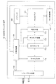
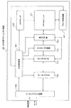
図1に示すように、本発明の実施の形態1に係るNAND型フラッシュメモリ装置100は、メモリセルアレイ101、ロウデコーダ102、カラムデコーダ103、選択回路104、センスアンプ回路105、主制御回路106、ブロック制御回路107、データレジスタ108及びインターフェイス回路109を具備している。
As shown in FIG. 1, the NAND
インターフェイス回路109は、外部機器とデータ及び制御信号(コマンド、トグル信号及びクロック信号など)の送受信を行う。インターフェイス回路109は、外部機器からのデータ及び制御信号を受けて所定の処理をして主制御回路106及びデータレジスタ108に与える。
The
主制御回路106は、インターフェイス回路109からの制御信号に基づいて、ロウデコーダ102、カラムデコーダ103、選択回路104、センスアンプ回路105、ブロック制御回路107及びデータレジスタ108を制御する。
The
主制御回路106は、ロウデコーダ102及びカラムデコーダ103にメモリセルアレイ101のメモリセルに対するアクセス情報を与える。ロウデコーダ102及びカラムデコーダ103は、当該アクセス情報及びデータに基づいてセンアンプ回路105、選択回路104及びブロック制御部107を制御してメモリセルに対してデータの読出、書込又は消去を行う。主制御回路106、ロウデコーダ102、カラムデコーダ103、センアンプ回路105、選択回路104及びブロック制御部107は、メモリセルアレイ101の複数のメモリセルに対しデータの書込及び読出を行う時に複数のワード線及び複数のビット線を選択して電圧を印加するデータ読出書込制御部を構成している。
The
図3に示すように、センスアンプ回路105は、複数のセンスアンプ1051を有し、メモリセルアレイ101のビット線に選択回路104を介して接続され、ビット線にデータを与え、かつ、ビット線の電位を検出してデータキャシュで保持する。主制御回路106は、カラムデコーダ103によって制御されたセンアンプ回路105によりメモリセルから読み出されたデータをデータレジスタ108及びインターフェイス回路109を介して外部機器に与える。選択回路104は、センスアンプ回路105を構成する複数のデータキャシュのうちビット線に接続するデータキャシュの選択を行う。
As shown in FIG. 3, the
次に、本発明の実施の形態1に係るNAND型フラッシュメモリ装置100のメモリセルアレイ101の1例について、図面を参照して詳細に説明する。
Next, an example of the
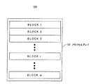
図2は、本発明の実施の形態1に係るメモリセルアレイ101の1例を示すブロック図である。図2に示すように、メモリセルアレイ101は、分割されているm個のブロックBLOCK1、BLOCK2、BLOCK3、・・・、BLOCKi、・・・、BLOCKmを具備している。ここで、「ブロック」とは、データの一括消去の最小単位である。ブロックBLOCK1、BLOCK2、BLOCK3、・・・、BLOCKi、・・・、BLOCKmは、同じ構成を有している。
FIG. 2 is a block diagram showing an example of the
メモリセルアレイ101は、電気的に書き換え可能な複数のメモリセルがマトリクス状に配置され、かつ、複数のNANDメモリセルユニットを有する。複数のワード線及び複数のビット線は、前記複数のメモリセルに接続されている。前記データ読出書込制御部は、前記複数のメモリセルに対しデータの書込、読出及び消去を行う時に前記複数のワード線及び前記複数のビット線を選択して電圧を印加する。
The
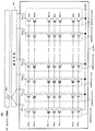
図3は、メモリセルアレイ101の1つのブロックBLOCKiの構成を示す回路図である。図3に示すように、メモリセルアレイ101のブロックBLOCKiは、2×k個のNANDセルユニットe1〜okを具備している。
FIG. 3 is a circuit diagram showing a configuration of one block BLOCKi of the
図3に示すNANDセルユニットe1〜okの各々は、32個のメモリセルMC0〜MC31を有している。メモリセルMC0〜MC31の1つは、代表してメモリセルMCと記される場合もある。メモリセルMC0〜MC31は、直列に接続されている。NANDセルユニットe1〜okの一端部は、選択ゲートトランジスタSGDを介してビット線BLe−1、BLo−1 、BLe−2、BLo−2、・・・、BLe−i、BLo−i、・・・、BLe−k、BLo−kに接続されている。
Each of the NAND cell units e1 to ok shown in FIG. 3 has 32 memory cells MC0 to MC31. One of the memory cells MC0 to MC31 may be represented as a memory cell MC as a representative. Memory cells MC0 to MC31 are connected in series. One ends of the NAND cell units e1 to ok are connected to the bit lines BLe - 1,
選択ゲートトランジスタSGDの制御ゲート電極は、選択ゲート線SGD−iに接続されている。また、NANDセルユニットe1〜okの他端部は、選択ゲートトランジスタSGSを介して共通ソース線CELSRCに接続されている。選択ゲートトランジスタSGSの制御ゲート電極は、選択ゲート線SGS−iに接続されている。 The control gate electrode of the selection gate transistor SGD is connected to the selection gate line SGD - i. Further, the other end portions of the NAND cell units e1 to ok are connected to the common source line CELSRC via the selection gate transistor SGS. The control gate electrode of the selection gate transistor SGS is connected to the selection gate line SGS - i.
メモリセルMC0〜MC31の各々の制御ゲート電極は、ワード線WL(WL0−i〜WL31−i)に接続されている。ビット線BLe−1、BLe−2、・・・、BLe−i、・・・、BLe−kのうちの端から数えて偶数番目のビット線と奇数番目のビット線は、お互いに独立にデータの書き込みと読み出しが行われる。ワード線WLn−iの1つに接続される2×k個のメモリセルMCの偶数番目のビット線に接続されているk個のメモリセルMCに対して同時にデータの書き込みと読み出しが行われる。k個のメモリセルMCの各々は、例えば、2ビット(4値)のデータを記憶する。これらのk個のメモリセルMCは、「ページ」という単位を構成する。
Each of the control gate electrode of the memory cell MC0~MC31 the word lines WL are connected to (WL0 - i - i~WL31). The bit lines BLe - 1,
同様に、ワード線WLn−iの1つに接続される2×k個のメモリセルMCの奇数番目のビット線に接続されているk個のメモリセルMCに対して同時にデータの書き込みと読み出しが行われる。k個のメモリセルMCの各々は、例えば、2ビット(4値)のデータを記憶する。これらのk個のメモリセルMCもまた、「ページ」という単位を構成する。 Similarly, data writing and reading are simultaneously performed on k memory cells MC connected to odd-numbered bit lines of 2 × k memory cells MC connected to one of word lines WLn − i. Done. Each of the k memory cells MC stores, for example, 2-bit (4-value) data. These k memory cells MC also constitute a unit called “page”.
なお、本発明は、図示した本発明の実施の形態1に限定されるものでなく、必要に応じてブロックの数、NANDセルユニットの数、直列メモリセル数、及びメモリセルの個数を変更してもよい。また、本発明の実施の形態1においては、各メモリセルMCが2ビット(4値)のデータを記憶するものである。すなわち、データ読出書込制御部は、各ページのアッパー(上位)ページ及びロウアー(下位)ページに対しデータの書込及び読出を行うことができる。また、データ読出書込制御部は、各偶数ページ及び各奇数ページのアッパー(上位)ページ及びロウアー(下位)ページに対しデータの書込及び読出を行うことができる。 The present invention is not limited to the illustrated first embodiment of the present invention, and the number of blocks, the number of NAND cell units, the number of serial memory cells, and the number of memory cells are changed as necessary. May be. In the first embodiment of the present invention, each memory cell MC stores 2-bit (4-level) data. In other words, the data read / write control unit can write and read data to and from the upper (upper) page and lower (lower) page of each page. The data read / write control unit can write and read data to the upper (upper) page and the lower (lower) page of each even page and each odd page.
センスアンプ回路105は、複数のセンスアンプ1051を具備している。複数のセンスアンプ1051の各々は、選択回路104を介してビット線BLe−1、BLe−2、・・・、BLe−i、・・・、BLe−kあるいは、BLo−1、BLo−2、・・・、BLo−i、・・・、BLo−kから構成される2つのビット線グループのいずれか一方に選択的に接続される。このセンスアンプ1051は、ビット線シールド型のセンスアンプと呼ばれている。
The
選択回路104は、選択情報に基づいて、2つのビット線グループの一方のみを選択してセンスアンプ1051に接続し、かつ、前記2つのビット線グループの他方を非選択としてセンスアンプ1051に接続しない。この場合には、選択回路104は、データの読み出し時には非選択側のビット線を接地することにより隣接のビット線の間の結合ノイズを低減している。また、選択回路104は、プログラム動作においては、非選択側のビット線をVDDにすることにより非選択のメモリセルMCにデータが書き込まれないようにする。
Based on the selection information, the
主制御回路106、ロウデコーダ102、カラムデコーダ103、センアンプ回路105、選択回路104及びブロック制御部107(前記データ読出書込制御部)は、メモリセルアレイ101の複数のメモリセルMCに対しデータの書込、読出及び消去を行う時に選択ブロック内の複数のワード線及び複数のビット線を選択して電圧を印加する。
The
そして、本発明の実施の形態1に係るNAND型フラッシュメモリ装置100においては、主制御回路106、ロウデコーダ102、カラムデコーダ103、センアンプ回路105、選択回路104及びブロック制御部107(前記データ読出書込制御部)は、選択ゲートトランジスタSGD及び選択ゲートトランジスタSGSに隣接するメモリセルMC31、MC0のデータを消去する消去動作時において当該メモリセルMC31、MC0の制御ゲート電極に接続されているワード線WL31−i、WL0−iに印加する消去ベリファイレベルを、当該メモリセルMC31、MC0以外の他の前記メモリセルの制御ゲート電極に接続されている他のワード線に印加する所定の消去電圧レベルより第1及び第2の所定値だけ低く設定する。
In the NAND
このように、前記データ読出書込制御部は、メモリセルMC31、MC0のデータを消去する消去動作時にワード線WL31−i、WL0−iに印加する消去ベリファイレベルを、当該メモリセルMC31、MC0以外の他の前記メモリセルの制御ゲート電極に接続されている他のワード線に印加する所定の消去電圧レベルより第1及び第2の所定値だけ低く設定した状態で、メモリセルMC31、MC0のデータを消去する。
Thus, the data read-write control section, the erasing operation for erasing data of the memory cell MC31,
なお、本発明の実施の形態1は、偶数ページ及び奇数ページの区別を有しない形態で各ページのアッパー(上位)ページ及びロウアー(下位)ページに対しデータの書込及び読出を行う場合にも適用することができる。 The first embodiment of the present invention also applies to the case where data is written to and read from the upper (upper) page and lower (lower) page of each page in a form that does not distinguish between even pages and odd pages. Can be applied.
本発明の実施の形態1によれば、ワード線WL31−i、WL0−iに印加する消去ベリファイレベルを、他のワード線に印加する所定の消去電圧レベルより第1及び第2の所定値だけ低く設定するため、選択ゲートトランジスタSGD及び選択ゲートトランジスタSGSに隣接するメモリセルMC31、MC0の閾値分布が高い側に変化することを防止することができるから、データの誤書込を有効に防止することができる。 According to the first embodiment of the present invention, the erase verify level applied to the word lines WL31 - i and WL0 - i is set to the first and second predetermined values from the predetermined erase voltage level applied to the other word lines. Since the threshold value is set low, it is possible to prevent the threshold distribution of the memory cells MC31 and MC0 adjacent to the selection gate transistor SGD and the selection gate transistor SGS from changing to a higher side, and therefore, erroneous writing of data is effectively prevented. be able to.
(実施の形態2)
次に、本発明の実施の形態2について、図面を参照しながら詳細に説明する。図4は、本発明の実施の形態2に係るNAND型フラッシュメモリ装置の構成を示すブロック図である。本発明の実施の形態2においては、本発明の実施の形態1と同じ構成要素には同じ参照符号が付されてその説明が省略される。
(Embodiment 2)
Next, a second embodiment of the present invention will be described in detail with reference to the drawings. FIG. 4 is a block diagram showing a configuration of the NAND flash memory device according to the second embodiment of the present invention. In the second embodiment of the present invention, the same components as those in the first embodiment of the present invention are denoted by the same reference numerals, and the description thereof is omitted.
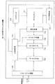
図4に示すように、本発明の実施の形態2に係るNAND型フラッシュメモリ装置200は、本発明の実施の形態1に係るNAND型フラッシュメモリ装置100において主制御回路106に代わりに主制御回路201を具備している。
As shown in FIG. 4, the NAND flash memory device 200 according to the second embodiment of the present invention includes a main control circuit in place of the
本発明の実施の形態2に係るNAND型フラッシュメモリ装置200は、メモリセルアレイ101、ロウデコーダ102、カラムデコーダ103、選択回路104、センスアンプ回路105、主制御回路201、ブロック制御回路107、データレジスタ108及びインターフェイス回路109を具備している。
The NAND flash memory device 200 according to the second embodiment of the present invention includes a
主制御回路201、ロウデコーダ102、カラムデコーダ103、センアンプ回路105、選択回路104及びブロック制御部107は、メモリセルアレイ101の複数のメモリセルに対しデータの書込及び読出を行う時に選択ブロック内の複数のワード線及び複数のビット線を選択して電圧を印加するデータ読出書込制御部を構成している。このデータ読出書込制御部は、ページごとにflag1を有している。このflag1は、各ページ(少なくともWL0、WL31のロウアーページ)が有するbitであり、ロウアーページデータの書き込みを行なわれたか否かを記憶しているbitである。ここで、flag1を有するロウアーページデータの書き込みが行なわれた時にflag1を記憶するセルは1(消去状態)から(書き込まれた状態)0とされる。すなわち、flag1=0である時に、flag1はロウアーページのデータの書き込みを行なわれたことを記憶しているものとする。また、データの書き込み順序は、各ページのロウアーページはアッパーページよりも先に行われ、偶数ページが奇数ページよりも先に行われるものとする。
The
本発明の実施の形態2においては、前記データ読出書込制御部は、選択ゲートトランジスタSGD及び選択ゲートトランジスタSGSに隣接するメモリセルMC31、MC0に対し偶数ページのロウアーページデータを書き込む書込動作時において当該メモリセルMC31、MC0の制御ゲート電極に接続されているワード線WL31−i、WL0−iに印加する書込ベリファイレベルを、当該メモリセルMC31、MC0以外の他の前記メモリセルの制御ゲート電極に接続されている他のワード線に印加する所定の書込電圧レベルより第1及び第2の所定値だけ低く設定する。 In the second embodiment of the present invention, the data read / write control unit performs a write operation of writing even page lower page data to the select gate transistor SGD and the memory cells MC31 and MC0 adjacent to the select gate transistor SGS. The write verify level applied to the word lines WL31 - i, WL0 - i connected to the control gate electrodes of the memory cells MC31, MC0 is set to the control gates of the memory cells other than the memory cells MC31, MC0. The first and second predetermined values are set lower than predetermined write voltage levels applied to other word lines connected to the electrodes.
また、本発明の実施の形態2においては、前記データ読出書込制御部は、選択ゲートトランジスタSGD及び選択ゲートトランジスタSGSに隣接するメモリセルMC31、MC0に対し偶数ページのロウアーページデータを読み出す読出動作時において当該奇数ページのロウアーページのデータが書き込まれていない時に当該メモリセルMC31、MC0の制御ゲート電極に接続されているワード線WL31−i、WL0−iに印加する読出ベリファイレベルを、当該メモリセルMC31、MC0以外の他の前記メモリセルの制御ゲート電極に接続されている他のワード線に印加する所定の読出電圧レベルより第3及び第4の所定値だけ低く設定する。 In the second embodiment of the present invention, the data read / write control unit reads the lower page data of the even pages from the selection gate transistor SGD and the memory cells MC31 and MC0 adjacent to the selection gate transistor SGS. The read verify level applied to the word lines WL31 - i, WL0 - i connected to the control gate electrodes of the memory cells MC31, MC0 when the odd page lower page data is not written is The third and fourth predetermined values are set lower than predetermined read voltage levels applied to other word lines connected to the control gate electrodes of the memory cells other than the cells MC31 and MC0.
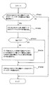
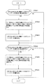
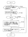
次に、本発明の実施の形態2に係る前記データ読出書込制御部の動作について、図5〜図8に基づいて具体的に説明する。図5は、本発明の実施の形態2に係る前記データ読出書込制御部のメモリセルMC0における偶数ページのロウアーページデータの書込動作の一部を説明するためのフローチャートである。図6は、本発明の実施の形態2に係る前記データ読出書込制御部のメモリセルMC31における偶数ページのロウアーページデータの書込動作の他の一部を説明するためのフローチャートである。図7は、本発明の実施の形態2に係る前記データ読出書込制御部のメモリセルMC0における偶数ページのロウアーページデータの読出動作の一部を説明するためのフローチャートである。図8は、本発明の実施の形態2に係る前記データ読出書込制御部のメモリセルMC31における偶数ページのロウアーページデータの読出動作の一部を説明するためのフローチャートである。 Next, the operation of the data read / write control unit according to the second embodiment of the present invention will be specifically described with reference to FIGS. FIG. 5 is a flowchart for explaining a part of an even page lower page data write operation in memory cell MC0 of data read / write control unit according to the second embodiment of the present invention. FIG. 6 is a flowchart for explaining another part of the write operation of the even page lower page data in the memory cell MC31 of the data read / write control unit according to the second embodiment of the present invention. FIG. 7 is a flowchart for explaining a part of the read operation of the even page lower page data in the memory cell MC0 of the data read / write control unit according to the second embodiment of the present invention. FIG. 8 is a flowchart for explaining a part of the read operation of even page lower page data in memory cell MC31 of the data read / write control unit according to the second embodiment of the present invention.
図5に示すように、ステップST101において、前記データ読出書込制御部は、メモリセルMC0に対し偶数ページのロウアーページデータを書き込む書込動作時であるかを判断する。 As shown in FIG. 5, in step ST101, the data read / write control unit determines whether it is a write operation for writing even page lower page data to the memory cell MC0.
ステップST101においてメモリセルMC0に対し偶数ページのロウアーページデータを書き込む書込動作時である場合に、前記データ読出書込制御部は、ワード線WL0−iに印加する書込ベリファイレベルを、他のワード線(ワード線WL31−iを除く)に印加する書込電圧レベルより第1の所定値だけ低く設定する(ステップST102)。 In step ST101, in the case of a write operation for writing even page lower page data to the memory cell MC0, the data read / write control unit sets the write verify level applied to the word line WL0 - i to another It is set lower by a first predetermined value than the write voltage level applied to the word lines (except word line WL31 - i) (step ST102).
次に、前記データ読出書込制御部は、メモリセルMC0に対し偶数ページのロウアーページデータを書き込む(ステップST103)。 Next, the data read / write controller writes even page lower page data to the memory cell MC0 (step ST103).
図6に示すように、ステップST201において、前記データ読出書込制御部は、メモリセルMC31に対し偶数ページのロウアーページデータを書き込む書込動作時であるかを判断する。 As shown in FIG. 6, in step ST201, the data read / write control unit determines whether it is a write operation for writing even page lower page data to the memory cell MC31.
ステップST201においてメモリセルMC31に対し偶数ページのロウアーページデータを書き込む書込動作時である場合に、前記データ読出書込制御部は、ワード線WL31−iに印加する書込ベリファイレベルを、他のワード線(ワード線WL0−iを除く)に印加する書込電圧レベルより第2の所定値だけ低く設定する(ステップST202)。 In step ST201, when the write operation is performed to write even page lower page data to the memory cell MC31, the data read / write control unit sets the write verify level to be applied to the word line WL31 - i to another level. It is set lower by a second predetermined value than the write voltage level applied to the word lines (excluding word lines WL0 - i) (step ST202).
次に、前記データ読出書込制御部は、メモリセルMC31に対し偶数ページのロウアーページデータを書き込む(ステップST203)。 Next, the data read / write control unit writes even page lower page data to the memory cell MC31 (step ST203).
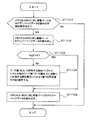
図7に示すように、ステップST301において、前記データ読出書込制御部は、MC0に対し偶数ページのロウアーページデータを読み出す読出動作時であるかを判断する。ステップST301においてMC0の偶数ページのロウアーページデータを読み出す読出動作時である場合に、前記データ読出書込制御部は、メモリセルMC0に対し奇数ページのロウアーページデータの読み出しを行う(ステップST302)。 As shown in FIG. 7, in step ST301, the data read / write control unit determines whether or not it is a read operation for reading even page lower page data from MC0. In the case of the read operation for reading the even page lower page data of MC0 in step ST301, the data read / write control unit reads the odd page lower page data from the memory cell MC0 (step ST302).
次に、前記データ読出書込制御部は、ステップST302のデータの読み出し結果に基づき、メモリセルMC0における奇数ページのロウアーページデータのflag1=0であるかを判断する(ステップST303)。 Next, the data read / write control unit determines whether flag1 = 0 of the odd page lower page data in the memory cell MC0 based on the data read result of step ST302 (step ST303).
ステップST303においてflag1=0でない時に、前記データ読出書込制御部は、ワード線WL0−iに印加する書込ベリファイレベルを、他のワード線(ワード線WL31−iを除く)に印加する書込電圧レベルより第3の所定値だけ低く設定する(ステップST304)。 When flag1 is not 0 in step ST303, the data read / write control unit writes the write verify level applied to the word lines WL0 - i to the other word lines (except for the word lines WL31 - i). It is set lower than the voltage level by a third predetermined value (step ST304).
ステップST303においてflag1=0である時、又は、ステップST304の後に、前記データ読出書込制御部は、メモリセルMC0に対し偶数ページのロウアーページデータを読み出す(ステップST305)。 When flag1 = 0 in step ST303, or after step ST304, the data read / write control unit reads even page lower page data from the memory cell MC0 (step ST305).
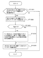
図8に示すように、ステップST401において、前記データ読出書込制御部は、MC31に対し偶数ページのロウアーページデータを読み出す読出動作時であるかを判断する。ステップST401においてMC31の偶数ページのロウアーページデータを読み出す時には、前記データ読出書込制御部は、メモリセルMC31に対し奇数ページのロウアーページデータの読み出しを行う(ステップST402)。 As shown in FIG. 8, in step ST401, the data read / write control unit determines whether or not it is a read operation for reading even page lower page data from the MC 31. When reading the even page lower page data of MC31 in step ST401, the data read / write control unit reads the odd page lower page data from the memory cell MC31 (step ST402).
次に、前記データ読出書込制御部は、ステップST402のデータの読み出し結果に基づき、メモリセルMC31における奇数ページのロウアーページデータのflag1=0であるかを判断する(ステップST403)。 Next, the data read / write control unit determines whether flag1 = 0 of the odd page lower page data in the memory cell MC31 is based on the data read result of step ST402 (step ST403).
ステップST403においてflag1=0でない時に、前記データ読出書込制御部は、ワード線WL31−iに印加する読出ベリファイレベルを、他のワード線(ワード線WL0−iを除く)に印加する読出電圧レベルより第3の所定値だけ低く設定する(ステップST404)。 When flag1 = 0 is not satisfied in step ST403, the data read / write control unit applies a read verify level applied to the word line WL31 - i to a read voltage level applied to other word lines (except for the word line WL0 - i). Further, it is set lower by a third predetermined value (step ST404).
ステップST403においてflag1=0である時、及び、ステップST404の後に、前記データ読出書込制御部は、メモリセルMC31に対し偶数ページのロウアーページデータを読み出す(ステップST405)。 When flag1 = 0 in step ST403 and after step ST404, the data read / write control unit reads even page lower page data from the memory cell MC31 (step ST405).
本発明の実施の形態2によれば、メモリセルMC31、MC0に対し偶数ページのロウアーページデータを書き込む書込動作時にワード線WL31−i、WL0−iに印加する書込ベリファイレベルを他のワード線に印加する所定の書込電圧レベルより第1及び第2の所定値だけ低く設定し、かつ、メモリセルMC31、MC0に対し偶数ページのロウアーページデータを読み出す読出動作時において当該奇数ページのロウアーページのデータが書き込まれていない時にワード線WL31−i、WL0−iに印加する読出ベリファイレベルを他のワード線に印加する所定の読出電圧レベルより第3及び第4の所定値だけ低く設定するため、選択ゲートトランジスタSGD及び選択ゲートトランジスタSGSに隣接するメモリセルMC31、MC0の閾値分布の変化をキャンセルすることができ、データの誤書込によるメモリセルのしきい値分布のシフトをキャンセルすることができる。
According to the second embodiment of the present invention, the memory cell MC31,
(実施の形態3)
次に、本発明の実施の形態3について、図面を参照しながら詳細に説明する。図9は、本発明の実施の形態3に係るNAND型フラッシュメモリ装置の構成を示すブロック図である。本発明の実施の形態3においては、本発明の実施の形態1と同じ構成要素には同じ参照符号が付されてその説明が省略される。
(Embodiment 3)
Next,
図9に示すように、本発明の実施の形態3に係るNAND型フラッシュメモリ装置300は、本発明の実施の形態1に係るNAND型フラッシュメモリ装置100において主制御回路106に代わりに主制御回路301を具備している。
As shown in FIG. 9, the NAND flash memory device 300 according to the third embodiment of the present invention is different from the
本発明の実施の形態3に係るNAND型フラッシュメモリ装置300は、メモリセルアレイ101、ロウデコーダ102、カラムデコーダ103、選択回路104、センスアンプ回路105、主制御回路301、ブロック制御回路107、データレジスタ108及びインターフェイス回路109を具備している。
The NAND flash memory device 300 according to the third embodiment of the present invention includes a
主制御回路301、ロウデコーダ102、カラムデコーダ103、センアンプ回路105、選択回路104及びブロック制御部107は、メモリセルアレイ101の複数のメモリセルに対しデータの書込及び読出を行う時に選択ブロック内の複数のワード線及び複数のビット線を選択して電圧を印加するデータ読出書込制御部を構成している。このデータ読出書込制御部は、ページごとにflag1を有している。
The
本発明の実施の形態3においては、前記データ読出書込制御部は、選択ゲートトランジスタSGD及び選択ゲートトランジスタSGSに隣接するメモリセルMC31、MC0に対し偶数ページのロウアーページデータを読み出す読出動作時において当該奇数ページのロウアーページのデータが書き込まれている時に当該メモリセルMC31、MC0の制御ゲート電極に接続されているワード線WL31−i、WL0−iに印加する読出レベルを、当該メモリセルMC31、MC0以外の他の前記メモリセルの制御ゲート電極に接続されている他のワード線に印加する所定の読出電圧レベルより第1及び第2の所定値だけ高く設定する。 In the third embodiment of the present invention, the data read / write control unit performs a read operation of reading even page lower page data to the select gate transistor SGD and the memory cells MC31 and MC0 adjacent to the select gate transistor SGS. The read level applied to the word lines WL31 - i, WL0 - i connected to the control gate electrodes of the memory cells MC31, MC0 when the odd page lower page data is written is set to the memory cell MC31, The first and second predetermined values are set higher than predetermined read voltage levels applied to other word lines connected to the control gate electrodes of the memory cells other than MC0.
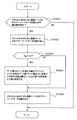
次に、本発明の実施の形態3に係る前記データ読出書込制御部の動作について、図10及び図11に基づいて具体的に説明する。図10は、本発明の実施の形態3に係る前記データ読出書込制御部のメモリセルMC0における偶数ページのロウアーページデータの読出動作の一部を説明するためのフローチャートである。図11は、本発明の実施の形態3に係る前記データ読出書込制御部のメモリセルMC31における偶数ページのロウアーページデータの読出動作の一部を説明するためのフローチャートである。 Next, the operation of the data read / write control unit according to the third embodiment of the present invention will be specifically described based on FIG. 10 and FIG. FIG. 10 is a flowchart for explaining a part of the read operation of the even page lower page data in the memory cell MC0 of the data read / write control unit according to the third embodiment of the present invention. FIG. 11 is a flowchart for explaining a part of the read operation of the even page lower page data in the memory cell MC31 of the data read / write control unit according to the third embodiment of the present invention.
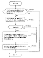
図10に示すように、ステップST501において、前記データ読出書込制御部は、MC0に対し偶数ページのロウアーページデータを読み出す読出動作時であるかを判断する。ステップST501においてMC0の偶数ページのロウアーページデータを読み出す読出動作時である場合に、前記データ読出書込制御部は、メモリセルMC0に対し奇数ページのロウアーページデータの読み出しを行う(ステップST502)。 As shown in FIG. 10, in step ST501, the data read / write control unit determines whether or not it is a read operation for reading even page lower page data from MC0. In step ST501, when the read operation is to read the even page lower page data of MC0, the data read / write control unit reads the odd page lower page data to the memory cell MC0 (step ST502).
次に、前記データ読出書込制御部は、ステップST502のデータの読み出し結果に基づき、メモリセルMC0における奇数ページのロウアーページデータのflag1=0であるかを判断する(ステップST503)。 Next, the data read / write control unit determines whether flag1 = 0 of the odd page lower page data in the memory cell MC0 based on the data read result of step ST502 (step ST503).
ステップST503においてflag1=0である時に、前記データ読出書込制御部は、ワード線WL0−iに印加する読出ベリファイレベルを、他のワード線(ワード線WL31−iを除く)に印加する読出電圧レベルより第1の所定値だけ高く設定する(ステップST504)。 When flag1 = 0 in step ST503, the data read / write control unit applies the read verify level applied to the word lines WL0 - i to the other word lines (excluding the word lines WL31 - i). It is set higher than the level by a first predetermined value (step ST504).
ステップST503においてflag1=0でない時、又は、ステップST504の後に、前記データ読出書込制御部は、メモリセルMC0に対し偶数ページのロウアーページデータを読み出す(ステップST505)。 When flag1 = 0 is not satisfied in step ST503 or after step ST504, the data read / write control unit reads even page lower page data from the memory cell MC0 (step ST505).
図11に示すように、ステップST601において、前記データ読出書込制御部は、MC31に対し偶数ページのロウアーページデータを読み出す読出動作時であるかを判断する。ステップST601においてMC31の偶数ページのロウアーページデータを読み出す読出動作時である場合に、前記データ読出書込制御部は、メモリセルMC31に対し奇数ページのロウアーページデータの読み出しを行う(ステップST602)。 As shown in FIG. 11, in step ST601, the data read / write control unit determines whether or not the MC 31 is in a read operation of reading even page lower page data. In the case of the read operation for reading the even page lower page data of MC31 in step ST601, the data read / write control unit reads the odd page lower page data to the memory cell MC31 (step ST602).
次に、前記データ読出書込制御部は、ステップST601のデータの読み出し結果に基づき、メモリセルMC31における奇数ページのロウアーページデータのflag1=0であるかを判断する(ステップST603)。 Next, the data read / write control unit determines whether flag1 = 0 of the odd page lower page data in the memory cell MC31 is based on the data read result of step ST601 (step ST603).
ステップST603においてflag1=0である時に、前記データ読出書込制御部は、ワード線WL31−iに印加する読出ベリファイレベルを、他のワード線(ワード線WL0−iを除く)に印加する読出電圧レベルより第2の所定値だけ高く設定する(ステップST604)。 When flag1 = 0 in step ST603, the data read / write control unit applies the read verify level applied to the word line WL31 - i to the other word lines (excluding the word lines WL0 - i). It is set higher than the level by a second predetermined value (step ST604).
ステップST603においてflag1=0でない時、及び、ステップST604の後に、前記データ読出書込制御部は、メモリセルMC31に対し偶数ページのロウアーページデータを読み出す(ステップST605)。 When flag1 = 0 is not satisfied in step ST603 and after step ST604, the data read / write control unit reads even page lower page data from the memory cell MC31 (step ST605).
本発明の実施の形態3によれば、メモリセルMC31、MC0に対し偶数ページのロウアーページデータを読み出す読出動作時において当該奇数ページのロウアーページのデータが書き込まれている時にワード線WL31−i、WL0−iに印加する読出ベリファイレベルを他のワード線に印加する所定の読出電圧レベルより第1及び第2の所定値だけ高く設定するため、選択ゲートトランジスタSGD及び選択ゲートトランジスタSGSに隣接するメモリセルMC31、MC0の閾値分布の変化をキャンセルすることができ、データの誤書込によるメモリセルのしきい値分布のシフトをキャンセルすることができる。 According to the third embodiment of the present invention, when the odd page lower page data is written in the read operation of reading the even page lower page data to the memory cells MC31, MC0, the word lines WL31 - i, A memory adjacent to the selection gate transistor SGD and the selection gate transistor SGS in order to set the read verification level applied to WL0 - i higher by a first and second predetermined values than a predetermined read voltage level applied to other word lines. Changes in the threshold distribution of the cells MC31 and MC0 can be canceled, and a shift in the threshold distribution of the memory cell due to erroneous data writing can be canceled.
(実施の形態4)
次に、本発明の実施の形態4について、図面を参照しながら詳細に説明する。図12は、本発明の実施の形態4に係るNAND型フラッシュメモリ装置の構成を示すブロック図である。本発明の実施の形態4においては、本発明の実施の形態1と同じ構成要素には同じ参照符号が付されてその説明が省略される。
(Embodiment 4)
Next, a fourth embodiment of the present invention will be described in detail with reference to the drawings. FIG. 12 is a block diagram showing a configuration of the NAND flash memory device according to the fourth embodiment of the present invention. In the fourth embodiment of the present invention, the same components as those in the first embodiment of the present invention are denoted by the same reference numerals, and the description thereof is omitted.
図12に示すように、本発明の実施の形態4に係るNAND型フラッシュメモリ装置400は、本発明の実施の形態1に係るNAND型フラッシュメモリ装置100において主制御回路106に代わりに主制御回路401を具備している。
As shown in FIG. 12, the NAND flash memory device 400 according to the fourth embodiment of the present invention is different from the
本発明の実施の形態4に係るNAND型フラッシュメモリ装置400は、メモリセルアレイ101、ロウデコーダ102、カラムデコーダ103、選択回路104、センスアンプ回路105、主制御回路401、ブロック制御回路107、データレジスタ108及びインターフェイス回路109を具備している。
The NAND flash memory device 400 according to the fourth embodiment of the present invention includes a
主制御回路401、ロウデコーダ102、カラムデコーダ103、センアンプ回路105、選択回路104及びブロック制御部107は、メモリセルアレイ101の複数のメモリセルに対しデータの書込及び読出を行う時に選択ブロック内の複数のワード線及び複数のビット線を選択して電圧を印加するデータ読出書込制御部を構成している。このデータ読出書込制御部は、ページごとにflag1を有している。また、このデータ読出書込制御部は、ページごとにflag2を有している。このflag2は、各ページ(少なくともWL0、WL31のアッパーページ)が有するbitであり、アッパーページのデータの書き込みを行ったか否かを記憶しているbitである。flag2を有するアッパーページデータの書き込みが行なわれた時にflag2を記憶するメモリセルは1(消去状態)から(書き込まれた状態)0とされる。すなわち、flag2=0である時に、flag2はアッパーページのデータの書き込みを行なわれたことを記憶しているものとする。また、メモリセルの信頼性をケアするために、flag2は、flag1と異なるセルにデータを記憶させることが望ましい。すなわち、flag1およびflag2を記憶するメモリセルは、2値データとしてデータを保持するのが望ましい。flag1およびflag2を同一のメモリセルに記憶(多値の記憶)させても、本発明は同様の効果が得られる。
The
本発明の実施の形態4においては、前記データ読出書込制御部は、選択ゲートトランジスタSGD及び選択ゲートトランジスタSGSに隣接するメモリセルMC31、MC0に対し偶数ページのアッパーページデータ、あるいは奇数ページのロウアーページデータを書き込む書込動作時において当該メモリセルMC31、MC0の制御ゲート電極に接続されているワード線WL31−i、WL0−iに印加する書込ベリファイレベルを、当該メモリセルMC31、MC0以外の他の前記メモリセルの制御ゲート電極に接続されている他のワード線に印加する所定の書込電圧レベルより偶数ページのアッパーページデータに対しては第1及び第2の所定値だけ低く設定し、奇数ページのロウアーページデータに対しては第3及び第4の所定値だけ低く設定する。 In the fourth embodiment of the present invention, the data read / write control unit performs the even page upper page data or the odd page lower page for the memory cells MC31 and MC0 adjacent to the select gate transistor SGD and the select gate transistor SGS. The write verify level applied to the word lines WL31 - i, WL0 - i connected to the control gate electrodes of the memory cells MC31, MC0 during the write operation for writing page data is set to a value other than that for the memory cells MC31, MC0. The upper page data of the even page is set lower than the predetermined write voltage level applied to the other word lines connected to the control gate electrodes of the other memory cells by the first and second predetermined values. 3rd and 4th predetermined values for lower page data of odd pages Set it only lower.
また、本発明の実施の形態4においては、前記データ読出書込制御部は、選択ゲートトランジスタSGD及び選択ゲートトランジスタSGSに隣接するメモリセルMC31、MC0に対し偶数ページのアッパーページデータを読み出す読出動作時において当該奇数ページのアッパーページデータが書き込まれていない時に当該メモリセルMC31、MC0の制御ゲート電極に接続されているワード線WL31−i、WL0−iに印加する読出ベリファイレベルを、当該メモリセルMC31、MC0以外の他の前記メモリセルの制御ゲート電極に接続されている他のワード線に印加する所定の読出電圧レベルより第5及び第6の所定値だけ低く設定する。 In the fourth embodiment of the present invention, the data read / write control unit reads the upper page data of the even page to the select gate transistor SGD and the memory cells MC31 and MC0 adjacent to the select gate transistor SGS. At this time, when the upper page data of the odd page is not written, the read verify level applied to the word lines WL31 - i, WL0 - i connected to the control gate electrodes of the memory cells MC31, MC0 is set to the memory cell. The fifth and sixth predetermined values are set lower than predetermined read voltage levels applied to other word lines connected to the control gate electrodes of the memory cells other than MC31 and MC0.
また、本発明の実施の形態4においては、前記データ読出書込制御部は、選択ゲートトランジスタSGD及び選択ゲートトランジスタSGSに隣接するメモリセルMC31、MC0に対し奇数ページのロウアーページデータを読み出す読出動作時において当該偶数ページのアッパーページデータが書き込まれていない時に当該メモリセルMC31、MC0の制御ゲート電極に接続されているワード線WL31−i、WL0−iに印加する読出ベリファイレベルを、当該メモリセルMC31、MC0以外の他の前記メモリセルの制御ゲート電極に接続されている他のワード線に印加する所定の読出電圧レベルより第7及び第8の所定値だけ低く設定する。 In the fourth embodiment of the present invention, the data read / write control unit reads the odd page lower page data to the memory cells MC31 and MC0 adjacent to the selection gate transistor SGD and the selection gate transistor SGS. At this time, when the even page upper page data is not written, the read verify level applied to the word lines WL31 - i, WL0 - i connected to the control gate electrodes of the memory cells MC31, MC0 is set to the memory cell. It is set lower by a seventh and eighth predetermined values than a predetermined read voltage level applied to other word lines connected to the control gate electrodes of the memory cells other than MC31 and MC0.
次に、本発明の実施の形態4に係る前記データ読出書込制御部の動作について、図13〜図18に基づいて具体的に説明する。図13は、本発明の実施の形態4に係る前記データ読出書込制御部のメモリセルMC0における偶数ページのアッパーページデータ、あるいはメモリセルMC0における奇数ページのロウアーページデータの書込動作の一部を説明するためのフローチャートである。図14は、本発明の実施の形態4係る前記データ読出書込制御部のメモリセルMC31における偶数ページのアッパーページデータ、あるいはメモリセルMC31における奇数ページのロウアーページデータの書込動作の一部を説明するためのフローチャートである。図15は、本発明の実施の形態4に係る前記データ読出書込制御部のメモリセルMC0における偶数ページのアッパーページデータの読出動作の一部を説明するためのフローチャートである。図16は、本発明の実施の形態4係る前記データ読出書込制御部のメモリセルMC31における偶数ページのアッパーページデータの読出動作の一部を説明するためのフローチャートである。図17は、本発明の実施の形態4に係る前記データ読出書込制御部のメモリセルMC0における奇数ページのロウアーページデータの読出動作の一部を説明するためのフローチャートである。図18は、本発明の実施の形態4係る前記データ読出書込制御部のメモリセルMC31における奇数ページのロウアーページデータの読出動作の一部を説明するためのフローチャートである。 Next, the operation of the data read / write control unit according to the fourth embodiment of the present invention will be specifically described with reference to FIGS. FIG. 13 shows a part of the write operation of the even page upper page data in the memory cell MC0 or the odd page lower page data in the memory cell MC0 of the data read / write control unit according to the fourth embodiment of the present invention. It is a flowchart for demonstrating. FIG. 14 shows a part of the write operation of the even page upper page data in the memory cell MC31 or the odd page lower page data in the memory cell MC31 of the data read / write control unit according to the fourth embodiment of the present invention. It is a flowchart for demonstrating. FIG. 15 is a flowchart for explaining a part of the read operation of the even page upper page data in the memory cell MC0 of the data read / write control unit according to the fourth embodiment of the present invention. FIG. 16 is a flowchart for explaining a part of the read operation of the even page upper page data in the memory cell MC31 of the data read / write control unit according to the fourth embodiment of the present invention. FIG. 17 is a flowchart for explaining a part of the read operation of lower page data of odd pages in the memory cell MC0 of the data read / write control unit according to the fourth embodiment of the present invention. FIG. 18 is a flowchart for explaining a part of the read operation of the odd page lower page data in the memory cell MC31 of the data read / write control unit according to the fourth embodiment of the present invention.
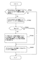
図13に示すように、ステップST701において、前記データ読出書込制御部は、メモリセルMC0に対し偶数ページのアッパーページデータを書き込む書込動作時であるかを判断する。 As shown in FIG. 13, in step ST701, the data read / write control unit determines whether it is a write operation for writing even page upper page data to the memory cell MC0.
ステップST701においてメモリセルMC0における偶数ページのアッパーページデータを書き込む書込動作時である場合に、前記データ読出書込制御部は、ワード線WL0−iに印加する書込ベリファイレベルを、他のワード線(ワード線WL31−iを除く)に印加する書込電圧レベルより第1の所定値だけ低く設定する(ステップST702)。 In step ST701, when it is a write operation to write even page upper page data in the memory cell MC0, the data read / write control unit sets the write verify level to be applied to the word line WL0 - i to another word. It is set lower by a first predetermined value than the write voltage level applied to the line (except for word line WL31 - i) (step ST702).
次に、前記データ読出書込制御部は、メモリセルMC0に対し偶数ページのアッパーページデータを書き込む(ステップST703)。 Next, the data read / write control unit writes even page upper page data to the memory cell MC0 (step ST703).
ステップST701においてメモリセルMC0における偶数ページのアッパーページデータを書き込む書込動作時でない場合、又は、ステップST703の後に、前記データ読出書込制御部は、メモリセルMC0に対し奇数ページのロウアーページデータを書き込む書込動作時であるかを判断する(ステップST704)。 In step ST701, when the write operation is not performed to write the even page upper page data in the memory cell MC0, or after step ST703, the data read / write control unit supplies the odd page lower page data to the memory cell MC0. It is determined whether the writing operation is in progress (step ST704).
ステップST704においてメモリセルMC0に対し奇数ページのロウアーページデータを書き込む書込動作時である場合に、前記データ読出書込制御部は、ワード線WL0−iに印加する書込ベリファイレベルを、他のワード線(ワード線WL31−iを除く)に印加する書込電圧レベルより第3の所定値だけ低く設定する(ステップST705)。 In step ST704, when the write operation for writing the odd page lower page data to the memory cell MC0 is performed, the data read / write control unit sets the write verify level applied to the word line WL0 - i to It is set lower by a third predetermined value than the write voltage level applied to the word lines (excluding word line WL31 - i) (step ST705).
次に、前記データ読出書込制御部は、メモリセルMC0に対し奇数ページのロウアーページデータを書き込む(ステップST706)。 Next, the data read / write controller writes odd page lower page data to the memory cell MC0 (step ST706).
図14に示すように、ステップST801において、前記データ読出書込制御部は、メモリセルMC31に対し偶数ページのアッパーページデータを書き込む書込動作時であるかを判断する。 As shown in FIG. 14, in step ST801, the data read / write control unit determines whether it is a write operation for writing even page upper page data into the memory cell MC31.
ステップST801においてメモリセルMC31における偶数ページのアッパーページデータを書き込む書込動作時である場合に、前記データ読出書込制御部は、ワード線WL31−iに印加する書込ベリファイレベルを、他のワード線(ワード線WL0−iを除く)に印加する書込電圧レベルより第2の所定値だけ低く設定する(ステップST802)。 In step ST801, when it is a write operation to write even page upper page data in the memory cell MC31, the data read / write control unit sets the write verify level to be applied to the word line WL31 - i to another word. It is set lower by a second predetermined value than the write voltage level applied to the lines (excluding word lines WL0 - i) (step ST802).
次に、前記データ読出書込制御部は、メモリセルMC31に対し偶数ページのアッパーページデータを書き込む(ステップST803)。 Next, the data read / write controller writes even page upper page data to the memory cell MC31 (step ST803).
ステップST801においてメモリセルMC31における偶数ページのアッパーページデータを書き込む書込動作時でない場合、又は、ステップST803の後に、前記データ読出書込制御部は、メモリセルMC31に対し奇数ページのロウアーページデータを書き込む書込動作時であるかを判断する(ステップST804)。 In step ST801, when it is not a write operation for writing even page upper page data in the memory cell MC31, or after step ST803, the data read / write control unit supplies the odd page lower page data to the memory cell MC31. It is determined whether the writing operation is in progress (step ST804).
ステップST804においてメモリセルMC31に対し奇数ページのロウアーページデータを書き込む書込動作時である場合に、前記データ読出書込制御部は、ワード線WL31−iに印加する書込ベリファイレベルを、他のワード線(ワード線WL0−iを除く)に印加する書込電圧レベルより第4の所定値だけ低く設定する(ステップST805)。 In step ST804, when the write operation for writing odd page lower page data to the memory cell MC31 is in progress, the data read / write control unit sets the write verify level to be applied to the word line WL31 - i to It is set lower by a fourth predetermined value than the write voltage level applied to the word lines (excluding word lines WL0 - i) (step ST805).
次に、前記データ読出書込制御部は、メモリセルMC31に対し奇数ページのロウアーページデータを書き込む(ステップST806)。 Next, the data read / write controller writes odd page lower page data to the memory cell MC31 (step ST806).
図15に示すように、ステップST901において、前記データ読出書込制御部は、メモリセルMC0に対し偶数ページのアッパーページデータを読み出す読出動作時であるかを判断する。 As shown in FIG. 15, in step ST901, the data read / write control unit determines whether or not it is during a read operation of reading even page upper page data from the memory cell MC0.
ステップST901においてメモリセルMC0に対し偶数ページのアッパーページデータを読み出す読出動作時である場合に、前記データ読出書込制御部は、メモリセルMC0に対し奇数ページのアッパーページデータの読み出しを行う(ステップST902)。 In step ST901, when the read operation is to read even page upper page data from the memory cell MC0, the data read / write control unit reads odd page upper page data from the memory cell MC0 (step ST901). ST902).
次に、前記データ読出書込制御部は、ステップST902のデータの読み出し結果に基づき、メモリセルMC0における奇数ページのアッパーページデータのflag2=0であるかを判断する(ステップST903)。 Next, the data read / write control unit determines whether flag2 = 0 of the odd page upper page data in the memory cell MC0 based on the data read result of step ST902 (step ST903).
ステップST903においてflag2=0でない時に、前記データ読出書込制御部は、ワード線WL0−iに印加する読出ベリファイレベルを、他のワード線(ワード線WL31−iを除く)に印加する読出電圧レベルより第5の所定値だけ低く設定する(ステップST904)。 When flag2 = 0 is not satisfied in step ST903, the data read / write control unit applies a read verify level applied to the word line WL0 - i to a read voltage level applied to other word lines (except for the word line WL31 - i). Is set lower by a fifth predetermined value (step ST904).
ステップST903においてflag2=0である時、及び、ステップST904の後に、前記データ読出書込制御部は、メモリセルMC0に対し偶数ページのアッパーページデータを読み出す(ステップST905)。 When flag2 = 0 in step ST903 and after step ST904, the data read / write control unit reads even page upper page data from the memory cell MC0 (step ST905).
図16に示すように、ステップST1001において、前記データ読出書込制御部は、MC31に対し偶数ページのアッパーページデータを読み出す読出動作時であるかを判断する。 As shown in FIG. 16, in step ST1001, the data read / write control unit determines whether or not the MC 31 is in a read operation for reading even page upper page data.
ステップST1001においてMC31に対し偶数ページのアッパーページデータを読み出す読出動作時である場合に、前記データ読出書込制御部は、メモリセルMC31に対し奇数ページのアッパーページデータの読み出しを行う(ステップST1002)。 In step ST1001, when the read operation is to read even page upper page data from MC31, the data read / write control unit reads odd page upper page data from memory cell MC31 (step ST1002). .
次に、前記データ読出書込制御部は、ステップST1002のデータの読み出し結果に基づき、メモリセルMC31における奇数ページのアッパーページデータのflag2=0であるかを判断する(ステップST1003)。 Next, the data read / write control unit determines whether flag2 = 0 of the odd page upper page data in the memory cell MC31 based on the data read result of step ST1002 (step ST1003).
ステップST1003においてflag2=0でない時に、前記データ読出書込制御部は、ワード線WL31−iに印加する読出ベリファイレベルを、他のワード線(ワード線WL0−iを除く)に印加する読出電圧レベルより第6の所定値だけ低く設定する(ステップST1004)。 When flag2 = 0 is not satisfied in step ST1003, the data read / write control unit applies a read verify level applied to the word line WL31 - i to a read voltage level applied to other word lines (excluding the word lines WL0 - i). Is set lower by a sixth predetermined value (step ST1004).
ステップST1003においてflag2=0である時、又は、ステップST1004の後に、前記データ読出書込制御部は、メモリセルMC31に対し偶数ページのアッパーページデータを読み出す(ステップST1005)。 When flag2 = 0 in step ST1003, or after step ST1004, the data read / write controller reads even page upper page data from the memory cell MC31 (step ST1005).
図17に示すように、ステップST1101において、前記データ読出書込制御部は、MC0に対し奇数ページのロウアーページデータを読み出す読出動作時であるかを判断する。 As shown in FIG. 17, in step ST1101, the data read / write control unit determines whether or not it is a read operation for reading lower page data of odd pages to MC0.
ステップST1101においてMC0に対し奇数ページのロウアーページデータを読み出す読出動作時である場合に、前記データ読出書込制御部は、メモリセルMC0に対し偶数ページのアッパーページデータの読み出しを行う(ステップST1102)。 In step ST1101, when the read operation is to read the odd page lower page data from MC0, the data read / write control unit reads the even page upper page data from the memory cell MC0 (step ST1102). .
次に、前記データ読出書込制御部は、ステップST1102のデータ読み出し結果に基づき、メモリセルMC0における偶数ページのアッパーページデータのflag2=0であるかを判断する(ステップST1103)。 Next, the data read / write control unit determines whether flag2 = 0 of the upper page data of the even page in the memory cell MC0 based on the data read result of step ST1102 (step ST1103).
ステップST1103においてflag2=0でない時に、前記データ読出書込制御部は、ワード線WL0−iに印加する読出ベリファイレベルを、他のワード線(ワード線WL31−iを除く)に印加する読出電圧レベルより第7の所定値だけ低く設定する(ステップST1104)。 When flag2 = 0 is not satisfied in step ST1103, the data read / write control unit applies a read verify level applied to the word line WL0 - i to a read voltage level applied to other word lines (excluding the word line WL31 - i). Is set lower by a seventh predetermined value (step ST1104).
ステップST1103においてflag2=0である時、又は、ステップST1104の後に、前記データ読出書込制御部は、メモリセルMC0に対し奇数ページのロウアーページデータを読み出す(ステップST1105)。 When flag2 = 0 in step ST1103, or after step ST1104, the data read / write control unit reads odd page lower page data from the memory cell MC0 (step ST1105).
図18に示すように、ステップST1201において、前記データ読出書込制御部は、MC31に対し奇数ページのロウアーページデータを読み出す読出動作時であるかを判断する。 As shown in FIG. 18, in step ST1201, the data read / write control unit determines whether or not it is a read operation for reading lower page data of odd pages to the MC 31.
ステップST1201においてMC31に対し奇数ページのロウアーページデータを読み出す読出動作時である場合に、前記データ読出書込制御部は、メモリセルMC31に対し偶数ページのアッパーページデータの読み出しを行う(ステップST1202)。 In step ST1201, when the read operation is to read the odd page lower page data from the MC 31, the data read / write control unit reads the even page upper page data from the memory cell MC31 (step ST1202). .
次に、前記データ読出書込制御部は、ステップST1202のデータの読み出し結果に基づき、メモリセルMC31における偶数ページのアッパーページデータのflag2=0であるかを判断する(ステップST1203)。 Next, the data read / write control unit determines whether flag2 = 0 of the even page upper page data in the memory cell MC31 is based on the data read result of step ST1202 (step ST1203).
ステップST1203においてflag2=0でない時に、前記データ読出書込制御部は、ワード線WL31−iに印加する読出ベリファイレベルを、他のワード線(ワード線WL0−iを除く)に印加する読出電圧レベルより第8の所定値だけ低く設定する(ステップST1204)。 When flag2 = 0 is not satisfied in step ST1203, the data read / write control unit applies a read verify level applied to the word line WL31 - i to a read voltage level applied to other word lines (excluding the word lines WL0 - i). Is set lower by an eighth predetermined value (step ST1204).
ステップST1203においてflag2=0である時、又は、ステップST1204の後に、前記データ読出書込制御部は、メモリセルMC31に対し奇数ページのロウアーページデータを読み出す(ステップST1205)。 When flag2 = 0 in step ST1203, or after step ST1204, the data read / write control unit reads odd page lower page data from the memory cell MC31 (step ST1205).
本発明の実施の形態4によれば、MC31、MC0に対し偶数ページのアッパーページデータ、あるいは奇数ページのロウアーページデータを書き込む書込動作時においてワード線WL31−i、WL0−iに印加する書込ベリファイレベルを他のワード線に印加する所定の書込電圧レベルより偶数ページのアッパーページデータに対しては第1及び第2の所定値だけ低く設定し、奇数ページのロウアーページデータに対しては第3及び第4の所定値だけ低く設定し、メモリセルMC31、MC0に対し偶数ページのアッパーページデータを読み出す読出動作時において当該奇数ページのアッパーページのデータが書き込まれていない時にワード線WL31−i、WL0−iに印加する読出ベリファイレベルを他のワード線に印加する所定の読出電圧レベルより第5及び第6の所定値だけ低く設定し、メモリセルMC31、MC0に対し奇数ページのロウアーページデータを読み出す読出動作時において当該偶数ページのアッパーページのデータが書き込まれていない時にワード線WL31−i、WL0−iに印加する読出ベリファイレベルをワード線に印加する所定の読出電圧レベルより第7及び第8の所定値だけ低く設定するため、選択ゲートトランジスタSGD及び選択ゲートトランジスタSGSに隣接するメモリセルMC31、MC0の閾値分布の変化をキャンすることができ、データの誤書込によるメモリセルのしきい値分布のシフトを有効にキャンセルすることができる。 According to the fourth embodiment of the present invention, the write applied to the word lines WL31 - i and WL0 - i in the write operation for writing the even page upper page data or the odd page lower page data to MC31 and MC0. The built-in verify level is set lower than the predetermined write voltage level applied to other word lines by the first and second predetermined values for the even page upper page data, and for the odd page lower page data. Is set lower by the third and fourth predetermined values, and when the upper page data of the odd page is not written in the read operation of reading the upper page data of the even page from the memory cells MC31 and MC0, the word line WL31. - i, WL0 - applying a read verify level on the other word lines to be applied to the i The upper page data of the even page is written in the read operation for reading the lower page data of the odd page to the memory cells MC31 and MC0, which is set lower than the predetermined read voltage level by the fifth and sixth predetermined values. In order to set the read verify level applied to the word lines WL31 - i and WL0 - i lower by the seventh and eighth predetermined values than the predetermined read voltage level applied to the word lines when there is not, the selection gate transistor SGD and the selection gate Changes in the threshold distribution of the memory cells MC31 and MC0 adjacent to the transistor SGS can be canceled, and a shift in the threshold distribution of the memory cell due to erroneous data writing can be effectively canceled.
(実施の形態5)
次に、本発明の実施の形態5について、図面を参照しながら詳細に説明する。図19は、本発明の実施の形態5に係るNAND型フラッシュメモリ装置の構成を示すブロック図である。本発明の実施の形態5においては、本発明の実施の形態1と同じ構成要素には同じ参照符号が付されてその説明が省略される。
(Embodiment 5)
Next, a fifth embodiment of the present invention will be described in detail with reference to the drawings. FIG. 19 is a block diagram showing a configuration of the NAND flash memory device according to the fifth embodiment of the present invention. In the fifth embodiment of the present invention, the same components as those in the first embodiment of the present invention are denoted by the same reference numerals, and the description thereof is omitted.
図19に示すように、本発明の実施の形態5に係るNAND型フラッシュメモリ装置500は、本発明の実施の形態1に係るNAND型フラッシュメモリ装置100において主制御回路106に代わりに主制御回路501を具備している。
As shown in FIG. 19, the NAND flash memory device 500 according to the fifth embodiment of the present invention is different from the
本発明の実施の形態5に係るNAND型フラッシュメモリ装置500は、メモリセルアレイ101、ロウデコーダ102、カラムデコーダ103、選択回路104、センスアンプ回路105、主制御回路501、ブロック制御回路107、データレジスタ108及びインターフェイス回路109を具備している。
The NAND flash memory device 500 according to the fifth embodiment of the present invention includes a
主制御回路501、ロウデコーダ102、カラムデコーダ103、センアンプ回路105、選択回路104及びブロック制御部107は、メモリセルアレイ101の複数のメモリセルに対しデータの書込及び読出を行う時に選択ブロック内の複数のワード線及び複数のビット線を選択して電圧を印加するデータ読出書込制御部を構成している。このデータ読出書込制御部は、ページごとにflag1を有している。また、このデータ読出書込制御部は、ページごとにflag2を有している。
The
本発明の実施の形態5においては、前記データ読出書込制御部は、選択ゲートトランジスタSGD及び選択ゲートトランジスタSGSに隣接するメモリセルMC31、MC0に対し偶数ページのアッパーページデータを読み出す読出動作時において当該奇数ページのアッパーページデータが書き込まれている時に当該メモリセルMC31、MC0の制御ゲート電極に接続されているワード線WL31−i、WL0−iに印加する読出ベリファイレベルを、当該メモリセルMC31、MC0以外の他の前記メモリセルの制御ゲート電極に接続されている他のワード線に印加する所定の読出電圧レベルより第1及び第2の所定値だけ高く設定する。 In the fifth embodiment of the present invention, the data read / write control unit performs a read operation of reading even page upper page data from the select gate transistor SGD and the memory cells MC31 and MC0 adjacent to the select gate transistor SGS. When the odd page upper page data is written, the read verify level applied to the word lines WL31 - i, WL0 - i connected to the control gate electrodes of the memory cells MC31, MC0 is set to the memory cell MC31, The first and second predetermined values are set higher than predetermined read voltage levels applied to other word lines connected to the control gate electrodes of the memory cells other than MC0.
また、本発明の実施の形態5においては、前記データ読出書込制御部は、メモリセルMC31、MC0に対し奇数ページのロウアーページデータを読み出す読出動作時において偶数ページのアッパーページデータが書き込まれている時に当該メモリセルMC31、MC0の制御ゲート電極に接続されているワード線WL31−i、WL0−iに印加する読出ベリファイレベルを、当該メモリセルMC31、MC0以外の他の前記メモリセルの制御ゲート電極に接続されている他のワード線に印加する所定の読出電圧レベルより第3及び第4の所定値だけ高く設定する。 In the fifth embodiment of the present invention, the data read / write control unit writes even page upper page data to the memory cells MC31 and MC0 during a read operation of reading odd page lower page data. The read verify level applied to the word lines WL31 - i, WL0 - i connected to the control gate electrodes of the memory cells MC31, MC0 is set to the control gates of the memory cells other than the memory cells MC31, MC0. The third and fourth predetermined values are set higher than predetermined read voltage levels applied to other word lines connected to the electrodes.
次に、本発明の実施の形態5に係る前記データ読出書込制御部の動作について、図20〜図23に基づいて具体的に説明する。図20は、本発明の実施の形態5に係る前記データ読出書込制御部のメモリセルMC0における偶数ページのアッパーページデータの読出動作の一部を説明するためのフローチャートである。図21は、本発明の実施の形態5係る前記データ読出書込制御部のメモリセルMC31における偶数ページのアッパーページデータの読出動作の一部を説明するためのフローチャートである。図22は、本発明の実施の形態5に係る前記データ読出書込制御部のメモリセルMC0における奇数ページのロウアーページデータの読出動作の一部を説明するためのフローチャートである。図23は、本発明の実施の形態5係る前記データ読出書込制御部のメモリセルMC31における奇数ページのロウアーページデータの読出動作の他の一部を説明するためのフローチャートである。 Next, the operation of the data read / write control unit according to the fifth embodiment of the present invention will be specifically described with reference to FIGS. FIG. 20 is a flowchart for explaining a part of the read operation of even page upper page data in memory cell MC0 of the data read / write control unit according to the fifth embodiment of the present invention. FIG. 21 is a flowchart for explaining a part of the read operation of the even page upper page data in the memory cell MC31 of the data read / write control unit according to the fifth embodiment of the present invention. FIG. 22 is a flowchart for explaining a part of the read operation of lower page data of odd pages in memory cell MC0 of the data read / write control unit according to the fifth embodiment of the present invention. FIG. 23 is a flowchart for explaining another part of the read operation of the odd page lower page data in the memory cell MC31 of the data read / write control unit according to the fifth embodiment of the present invention.
図20に示すように、ステップST1301において、前記データ読出書込制御部は、メモリセルMC0に対し偶数ページのアッパーページデータを読み出す読出動作時であるかを判断する。 As shown in FIG. 20, in step ST1301, the data read / write control unit determines whether or not it is during a read operation of reading even page upper page data from the memory cell MC0.
ステップST1301においてメモリセルMC0に対し偶数ページのアッパーページデータを読み出す読出動作時である場合に、前記データ読出書込制御部は、メモリセルMC0に対し奇数ページのアッパーページデータの読み出しを行う(ステップST1302)。 In step ST1301, in the read operation for reading the even page upper page data from the memory cell MC0, the data read / write control unit reads the odd page upper page data from the memory cell MC0 (step ST1301). ST1302).
次に、前記データ読出書込制御部は、ステップST1302のデータの読み出し結果に基づき、メモリセルMC0における奇数ページのアッパーページデータflag2=0であるかを判断する(ステップST1303)。 Next, the data read / write control unit determines whether or not the odd page upper page data flag2 = 0 in the memory cell MC0 based on the data read result of step ST1302 (step ST1303).
ステップST1303においてflag2=0である時、前記データ読出書込制御部は、ワード線WL0−iに印加する読出ベリファイレベルを、他のワード線(ワード線WL31−iを除く)に印加する読出電圧レベルより第3の所定値だけ高く設定する(ステップST1304)。 When flag2 = 0 in step ST1303, the data read / write control unit applies the read verify level applied to the word lines WL0 - i to the other word lines (excluding the word lines WL31 - i). It is set higher than the level by a third predetermined value (step ST1304).
ステップST1303においてflag2=0でない時、又は、ステップST1304の後に、前記データ読出書込制御部は、メモリセルMC0に対し偶数ページのアッパーページデータを読み出す(ステップST1305)。 When flag2 = 0 is not satisfied in step ST1303, or after step ST1304, the data read / write controller reads even page upper page data from the memory cell MC0 (step ST1305).
図21に示すように、ステップST1401において、前記データ読出書込制御部は、メモリセルMC31に対し偶数ページのアッパーページデータを読み出す読出動作時であるかを判断する。 As shown in FIG. 21, in step ST1401, the data read / write control unit determines whether or not it is during a read operation of reading even page upper page data from the memory cell MC31.
ステップST1401においてメモリセルMC31に対し偶数ページのアッパーページデータを読み出す読出動作時である場合に、前記データ読出書込制御部は、メモリセルMC31に対し奇数ページのアッパーページデータの読み出しを行う(ステップST1402)。 In step ST1401, when the read operation is to read even page upper page data from the memory cell MC31, the data read / write control unit reads odd page upper page data from the memory cell MC31 (step ST1401). ST1402).
次に、前記データ読出書込制御部は、ステップST1402のデータの読み出し結果に基づき、メモリセルMC31における奇数ページのアッパーページデータのflag2=0であるかを判断する(ステップST1403)。 Next, the data read / write control unit determines whether flag2 = 0 of the odd page upper page data in the memory cell MC31 is based on the data read result of step ST1402 (step ST1403).
ステップST1403においてflag2=0である時、前記データ読出書込制御部は、ワード線WL31−iに印加する読出ベリファイレベルを、他のワード線(ワード線WL0−iを除く)に印加する読出電圧レベルより第4の所定値だけ高く設定する(ステップST1404)。 When flag2 = 0 in step ST1403, the data read / write control unit applies a read verify level applied to the word line WL31 - i to a read voltage applied to other word lines (except for the word line WL0 - i). It is set higher than the level by a fourth predetermined value (step ST1404).
ステップS1403においてflag2=0でない時、又は、ステップST1404の後に、前記データ読出書込制御部は、メモリセルMC31に対し偶数ページのアッパーページデータを読み出す(ステップST1405)。 When flag2 = 0 is not satisfied in step S1403, or after step ST1404, the data read / write control unit reads even page upper page data from the memory cell MC31 (step ST1405).
図22に示すように、ステップST1501において、前記データ読出書込制御部は、メモリセルMC0に対し奇数ページのロウアーページデータを読み出す読出動作時であるかを判断する。 As shown in FIG. 22, in step ST1501, the data read / write control unit determines whether or not it is during a read operation of reading odd page lower page data to the memory cell MC0.
ステップST1501においてメモリセルMC0に対し奇数ページのロウアーページデータを読み出す読出動作時である場合に、前記データ読出書込制御部は、メモリセルMC0に対し偶数ページのアッパーページデータの読み出しを行う(ステップST1502)。 In step ST1501, when the read operation is to read the odd page lower page data from the memory cell MC0, the data read / write control unit reads the even page upper page data from the memory cell MC0 (step ST1501). ST1502).
次に、前記データ読出書込制御部は、ステップST1502のデータの読み出し結果に基づき、メモリセルMC0における偶数ページのアッパーページデータのflag2=0であるかを判断する(ステップST1503)。 Next, the data read / write control unit determines whether flag2 = 0 of the even page upper page data in the memory cell MC0 based on the data read result of step ST1502 (step ST1503).
ステップST1503においてflag2=0である時に、前記データ読出書込制御部は、ワード線WL0−iに印加する読出ベリファイレベルを他のワード線(ワード線WL31−iを除く)に印加する読出電圧レベルより第5の所定値だけ高く設定する(ステップST1504)。 When flag2 = 0 in step ST1503, the data read / write control unit applies the read verify level applied to the word lines WL0 - i to the other word lines (excluding the word lines WL31 - i). Then, it is set higher by a fifth predetermined value (step ST1504).
ステップST1503においてflag2=0でない時、又は、ステップST1504の後に、前記データ読出書込制御部は、メモリセルMC0に対し奇数ページのロウアーページデータを読み出す(ステップST1505)。 When flag2 = 0 is not satisfied in step ST1503, or after step ST1504, the data read / write control unit reads odd page lower page data from the memory cell MC0 (step ST1505).
図23に示すように、ステップST1601において、前記データ読出書込制御部は、メモリセルMC31に対し奇数ページのロウアーページデータを読み出す読出動作時であるかを判断する。 As shown in FIG. 23, in step ST1601, the data read / write control unit determines whether or not it is during a read operation of reading odd page lower page data from the memory cell MC31.
ステップST1601においてメモリセルMC31に対し奇数ページのロウアーページデータを読み出す読出動作時である場合に、前記データ読出書込制御部は、メモリセルMC31に対し偶数ページのアッパーページデータの読み出しを行う(ステップST1602)。 In step ST1601, when the read operation is to read odd page lower page data from the memory cell MC31, the data read / write control unit reads even page upper page data from the memory cell MC31 (step ST1601). ST1602).
次に、前記データ読出書込制御部は、ステップST1602のデータの読み出し結果に基づき、メモリセルMC31における偶数ページのアッパーページデータのflag2=0であるかを判断する(ステップST1603)。 Next, the data read / write control unit determines whether flag2 = 0 of the even page upper page data in the memory cell MC31 based on the data read result of step ST1602 (step ST1603).
ステップST1603においてflag2=0である時に、前記データ読出書込制御部は、ワード線WL31−iに印加する読出ベリファイレベルを、他のワード線(ワード線WL0−iを除く)に印加する読出電圧レベルより第6の所定値だけ高く設定する(ステップST1604)。 When flag2 = 0 in step ST1603, the data read / write control unit applies the read verify level applied to the word line WL31 - i to the other word lines (excluding the word lines WL0 - i). It is set higher than the level by a sixth predetermined value (step ST1604).
ステップST1603においてflag2=0でない時、又は、ステップST1604の後に、前記データ読出書込制御部は、メモリセルMC31に対し奇数ページのロウアーページデータを読み出す(ステップST1605)。 When flag2 = 0 is not satisfied in step ST1603 or after step ST1604, the data read / write control unit reads odd page lower page data from the memory cell MC31 (step ST1605).
本発明の実施の形態5によれば、メモリセルMC31、MC0に対し偶数ページのアッパーページデータを読み出す読出動作時において当該奇数ページのアッパーページデータが書き込まれている時にワード線WL31−i、WL0−iに印加する読出ベリファイレベルを他のワード線に印加する所定の読出電圧レベルより第1及び第2の所定値だけ高く設定し、メモリセルMC31、MC0に対し奇数ページのロウアーページデータを読み出す読出動作時において当該偶数ページのアッパーページデータが書き込まれている時にワード線WL31−i、WL0−iに印加する読出ベリファイレベルを他のワード線に印加する所定の読出電圧レベルより第3及び第4の所定値だけ高く設定するため、選択ゲートトランジスタSGD及び選択ゲートトランジスタSGSに隣接するメモリセルMC31、MC0の閾値分布の変化をキャンセルすることができ、データの誤書込によるメモリセルのしきい値分布のシフトを有効にキャンセルすることができる。
According to the fifth embodiment of the present invention, when the odd page upper page data is written in the read operation of reading the even page upper page data from the memory cells MC31 and MC0, the word lines WL31 - i and WL0 are written. The read verify level applied to i is set higher by the first and second predetermined values than the predetermined read voltage level applied to the other word lines, and the odd page lower page data is read from the memory cells MC31 and MC0. In the read operation, when the upper page data of the even page is being written, the third and third read verify levels applied to the word lines WL31 - i and WL0 - i are higher than predetermined read voltage levels applied to other word lines. 4 to set it higher by a predetermined value of 4, select gate transistors SGD and Memory cell MC31 adjacent-option gate transistor SGS, it is possible to cancel the change in threshold distribution of
なお、本発明の実施の形態1〜実施の形態5において、前記消去ベリファイレベル、前記書込ベリファイレベル及び前記読出ベリファイレベルは、統計的な閾値分布の変化を計測して閾値分布変化分を求め、この閾値分布変化分に基づいて求めることができる。 In the first to fifth embodiments of the present invention, the erase verify level, the write verify level, and the read verify level are obtained by measuring a statistical threshold distribution change to obtain a threshold distribution change amount. The threshold distribution change can be obtained.
次に、前記書込電圧、読出電圧、消去電圧及びベリファイレベルの具体的な一例を説明する。前記書込電圧は20Vであり、書き込まないメモリセルのワード線には10Vの電圧が印加される。4値のデータの前記読出電圧は、1V、2V、3Vであり、読まないメモリセルのワード線には5Vの電圧が印加される。前記読出電圧に対して、それぞれのレベルの書込ベリファイレベルは0.3Vだけ高い。ベリファイレベルを高く又は低くする電圧変化量は0.05V(50mV)である。 Next, specific examples of the write voltage, read voltage, erase voltage, and verify level will be described. The write voltage is 20V, and a voltage of 10V is applied to the word lines of the memory cells not to be written. The read voltage of the quaternary data is 1V, 2V, and 3V, and a voltage of 5V is applied to the word line of the memory cell that is not read. The write verify level of each level is higher than the read voltage by 0.3V. The amount of voltage change for increasing or decreasing the verify level is 0.05 V (50 mV).
100、200、300、400、500 NAND型フラッシュメモリ装置
101 メモリセルアレイ
102 ロウデコーダ
103 カラムデコーダ
104 選択回路
105 センスアンプ回路
106、201、301、401、501 主制御回路
107 ブロック制御回路
108 データレジスタ
109 インターフェイス回路
100, 200, 300, 400, 500 NAND
Claims (5)
前記複数のNANDメモリセルユニットの各々は、
直列に接続されている前記複数のメモリセルと、前記複数のメモリセルの直列接続体の一端部と前記ビット線との間に接続されている第1の選択ゲートトランジスタと、前記複数のメモリセルの直列接続体の他端部とソース線との間に接続されている第2の選択ゲートトランジスタと、を具備し、
前記データ読出書込制御部は、
前記第1の選択ゲートトランジスタあるいは前記第2の選択ゲートトランジスタに隣接する前記メモリセルのデータを消去する消去動作時において当該メモリセルの制御ゲート電極に接続されているワード線に印加する消去ベリファイレベルを、当該メモリセル以外の他の前記メモリセルの制御ゲート電極に接続されている他のワード線に印加する所定の消去電圧レベルより第1及び第2の所定値だけ低く設定することを特徴とするNAND型フラッシュメモリ装置。 A plurality of electrically rewritable memory cells and a memory cell array having a plurality of NAND memory cell units; a plurality of word lines and a plurality of bit lines connected to the plurality of memory cells; A data read / write controller that selects and applies a voltage to the plurality of word lines and the plurality of bit lines when data is written to, read from, and erased from a plurality of memory cells;
Each of the plurality of NAND memory cell units includes:
The plurality of memory cells connected in series, a first select gate transistor connected between one end of the series connection body of the plurality of memory cells and the bit line, and the plurality of memory cells A second select gate transistor connected between the other end of the serial connection body and the source line,
The data read / write controller is
An erase verify level applied to a word line connected to a control gate electrode of the memory cell during an erase operation for erasing data of the memory cell adjacent to the first select gate transistor or the second select gate transistor Is set lower than a predetermined erase voltage level applied to another word line connected to the control gate electrode of the memory cell other than the memory cell by a first and second predetermined values. NAND flash memory device.
前記複数のNANDメモリセルユニットの各々は、
直列に接続されている前記複数のメモリセルと、前記複数のメモリセルの直列接続体の一端部と前記ビット線との間に接続されている第1の選択ゲートトランジスタと、前記複数のメモリセルの直列接続体の他端部とソース線との間に接続されている第2の選択ゲートトランジスタと、を具備し、
前記データ読出書込制御部は、
前記第1の選択ゲートトランジスタあるいは前記第2の選択ゲートトランジスタに隣接する前記メモリセルに対し偶数ページのロウアーページデータを書き込む書込動作時において当該メモリセルの制御ゲート電極に接続されているワード線に印加する書込ベリファイレベルを、当該メモリセル以外の他の前記メモリセルの制御ゲート電極に接続されている他のワード線に印加する所定の書込電圧レベルより第1及び第2の所定値だけ低く設定し、かつ、前記第1の選択ゲートトランジスタあるいは前記第2の選択ゲートトランジスタに隣接する前記メモリセルに対し偶数ページのロウアーページデータを読み出す読出動作時において当該奇数ページのロウアーページのデータが書き込まれていない時に当該メモリセルの制御ゲート電極に接続されているワード線に印加する読出ベリファイレベルを、当該メモリセル以外の他の前記メモリセルの制御ゲート電極に接続されている他のワード線に印加する所定の読出電圧レベルより第3及び第4の所定値だけ低く設定することを特徴とするNAND型フラッシュメモリ装置。 A plurality of electrically rewritable memory cells and a memory cell array having a plurality of NAND memory cell units; a plurality of word lines and a plurality of bit lines connected to the plurality of memory cells; A data read / write controller that selects and applies a voltage to the plurality of word lines and the plurality of bit lines when data is written to, read from, and erased from a plurality of memory cells;
Each of the plurality of NAND memory cell units includes:
The plurality of memory cells connected in series, a first select gate transistor connected between one end of the series connection body of the plurality of memory cells and the bit line, and the plurality of memory cells A second select gate transistor connected between the other end of the serial connection body and the source line,
The data read / write controller is
A word line connected to the control gate electrode of the memory cell during a write operation of writing even page lower page data to the memory cell adjacent to the first select gate transistor or the second select gate transistor The first and second predetermined values from the predetermined write voltage level applied to the other word lines connected to the control gate electrodes of the memory cells other than the memory cell The lower page data of the odd page in the read operation in which the even page lower page data is read from the memory cell adjacent to the first select gate transistor or the second select gate transistor. Is not written to the control gate electrode of the memory cell. The third and fourth read verify levels applied to the word lines that are applied to the other word lines connected to the control gate electrodes of the memory cells other than the memory cell are set to be third and fourth. A NAND flash memory device characterized by being set lower by a predetermined value.
前記複数のNANDメモリセルユニットの各々は、
直列に接続されている前記複数のメモリセルと、前記複数のメモリセルの直列接続体の一端部と前記ビット線との間に接続されている第1の選択ゲートトランジスタと、前記複数のメモリセルの直列接続体の他端部とソース線との間に接続されている第2の選択ゲートトランジスタと、を具備し、
前記データ読出書込制御部は、
前記第1の選択ゲートトランジスタあるいは前記第2の選択ゲートトランジスタに隣接する前記メモリセルに対し偶数ページのロウアーページデータを読み出す読出動作時において当該奇数ページのロウアーページデータが書き込まれている時に当該メモリセルの制御ゲート電極に接続されているワード線に印加する読出ベリファイレベルを、当該メモリセル以外の他の前記メモリセルの制御ゲート電極に接続されている他のワード線に印加する所定の読出電圧レベルより第1及び第2の所定値だけ高く設定することを特徴とするNAND型フラッシュメモリ装置。 A plurality of electrically rewritable memory cells and a memory cell array having a plurality of NAND memory cell units; a plurality of word lines and a plurality of bit lines connected to the plurality of memory cells; A data read / write controller that selects and applies a voltage to the plurality of word lines and the plurality of bit lines when data is written to, read from, and erased from a plurality of memory cells;
Each of the plurality of NAND memory cell units includes:
The plurality of memory cells connected in series, a first select gate transistor connected between one end of the series connection body of the plurality of memory cells and the bit line, and the plurality of memory cells A second select gate transistor connected between the other end of the serial connection body and the source line,
The data read / write controller is
When the lower page data of the odd page is written in the read operation of reading the lower page data of the even page to the memory cell adjacent to the first select gate transistor or the second select gate transistor. A predetermined read voltage applied to another word line connected to the control gate electrode of the memory cell other than the memory cell, as a read verify level applied to the word line connected to the control gate electrode of the cell A NAND flash memory device, wherein the first and second predetermined values are set higher than the level.
前記複数のNANDメモリセルユニットの各々は、
直列に接続されている前記複数のメモリセルと、前記複数のメモリセルの直列接続体の一端部と前記ビット線との間に接続されている第1の選択ゲートトランジスタと、前記複数のメモリセルの直列接続体の他端部とソース線との間に接続されている第2の選択ゲートトランジスタと、を具備し、
前記データ読出書込制御部は、
前記第1の選択ゲートトランジスタあるいは前記第2の選択ゲートトランジスタに隣接する前記メモリセルに対し偶数ページのアッパーページデータあるいは奇数ページのロウアーページデータを書き込む書込動作時において当該メモリセルの制御ゲート電極に接続されているワード線に印加する書込ベリファイレベルを、当該メモリセル以外の他の前記メモリセルの制御ゲート電極に接続されている他のワード線に印加する所定の書込電圧レベルより偶数ページのアッパーページデータに対しては第1及び第2の所定値だけ低く設定し、奇数ページのロウアーページデータに対しては第3および第4の所定値だけ低く設定し、
前記第1の選択ゲートトランジスタあるいは前記第2の選択ゲートトランジスタに隣接する前記メモリセルに対し偶数ページのアッパーページデータを読み出す読出動作時において当該奇数ページのアッパーページデータが書き込まれていない時に当該メモリセルの制御ゲート電極に接続されているワード線に印加する読出ベリファイレベルを、当該メモリセル以外の他の前記メモリセルの制御ゲート電極に接続されている他のワード線に印加する所定の読出電圧レベルより第5及び第6の所定値だけ低く設定し、
前記第1の選択ゲートトランジスタあるいは前記第2の選択ゲートトランジスタに隣接する前記メモリセルに対し奇数ページのロウアーページデータを読み出す読出動作時において当該偶数ページのアッパーページのデータが書き込まれていない時に当該メモリセルの制御ゲート電極に接続されているワード線に印加する読出ベリファイレベルを、当該メモリセル以外の他の前記メモリセルの制御ゲート電極に接続されている他のワード線に印加する所定の読出電圧レベルより第7及び第8の所定値だけ低く設定することを特徴とするNAND型フラッシュメモリ装置。 A plurality of electrically rewritable memory cells and a memory cell array having a plurality of NAND memory cell units; a plurality of word lines and a plurality of bit lines connected to the plurality of memory cells; A data read / write controller that selects and applies a voltage to the plurality of word lines and the plurality of bit lines when data is written to, read from, and erased from a plurality of memory cells;
Each of the plurality of NAND memory cell units includes:
The plurality of memory cells connected in series, a first select gate transistor connected between one end of the series connection body of the plurality of memory cells and the bit line, and the plurality of memory cells A second select gate transistor connected between the other end of the serial connection body and the source line,
The data read / write controller is
Control gate electrode of the memory cell in a write operation for writing even page upper page data or odd page lower page data to the memory cell adjacent to the first select gate transistor or the second select gate transistor The write verify level applied to the word line connected to the memory cell is an even number higher than a predetermined write voltage level applied to another word line connected to the control gate electrode of the memory cell other than the memory cell. Set lower for the upper page data of the page by the first and second predetermined values, set lower for the odd page lower page data by the third and fourth predetermined values,
When the odd page upper page data is not written in the read operation of reading the even page upper page data to the memory cell adjacent to the first select gate transistor or the second select gate transistor. A predetermined read voltage applied to another word line connected to the control gate electrode of the memory cell other than the memory cell, as a read verify level applied to the word line connected to the control gate electrode of the cell Set lower than the level by the fifth and sixth predetermined values,
When the even page upper page data is not written in the read operation of reading the odd page lower page data to the memory cell adjacent to the first select gate transistor or the second select gate transistor. A predetermined read level applied to a word line connected to a control gate electrode of a memory cell other than the memory cell is applied to a read verify level applied to the word line connected to the control gate electrode of the memory cell. A NAND type flash memory device, wherein the NAND type flash memory device is set lower than the voltage level by a seventh and eighth predetermined values.
前記複数のNANDメモリセルユニットの各々は、
直列に接続されている前記複数のメモリセルと、前記複数のメモリセルの直列接続体の一端部と前記ビット線との間に接続されている第1の選択ゲートトランジスタと、前記複数のメモリセルの直列接続体の他端部とソース線との間に接続されている第2の選択ゲートトランジスタと、を具備し、
前記データ読出書込制御部は、
前記第1の選択ゲートトランジスタあるいは前記第2の選択ゲートトランジスタに隣接する前記メモリセルに対し偶数ページのアッパーページデータを読み出す読出動作時において当該奇数ページのアッパーページデータが書き込まれている時に当該メモリセルの制御ゲート電極に接続されているワード線に印加する読出ベリファイレベルを、当該メモリセル以外の他の前記メモリセルの制御ゲート電極に接続されている他のワード線に印加するように所定の読出電圧レベルより第1及び第2の所定値だけ高く設定し、
前記第1の選択ゲートトランジスタあるいは前記第2の選択ゲートトランジスタに隣接する前記メモリセルに対し奇数ページのアッパーページデータを読み出す読出動作時において当該偶数ページのアッパーページデータが書き込まれている時に当該メモリセルの制御ゲート電極に接続されているワード線に印加する読出ベリファイレベルを、当該メモリセル以外の他の前記メモリセルの制御ゲート電極に接続されている他のワード線に印加する所定の読出電圧レベルより第3及び第4の所定値だけ高く設定することを特徴とするNAND型フラッシュメモリ装置。 A plurality of electrically rewritable memory cells and a memory cell array having a plurality of NAND memory cell units; a plurality of word lines and a plurality of bit lines connected to the plurality of memory cells; A data read / write controller that selects and applies a voltage to the plurality of word lines and the plurality of bit lines when data is written to, read from, and erased from a plurality of memory cells;
Each of the plurality of NAND memory cell units includes:
The plurality of memory cells connected in series, a first select gate transistor connected between one end of the series connection body of the plurality of memory cells and the bit line, and the plurality of memory cells A second select gate transistor connected between the other end of the serial connection body and the source line,
The data read / write controller is
When the upper page data of the odd page is written in the read operation for reading the upper page data of the even page to the memory cell adjacent to the first selection gate transistor or the second selection gate transistor, the memory A predetermined read verify level applied to the word line connected to the control gate electrode of the cell is applied to another word line connected to the control gate electrode of the memory cell other than the memory cell. Set higher than the read voltage level by the first and second predetermined values,
When the even page upper page data is written in the read operation of reading the odd page upper page data to the memory cell adjacent to the first select gate transistor or the second select gate transistor. A predetermined read voltage applied to another word line connected to the control gate electrode of the memory cell other than the memory cell, as a read verify level applied to the word line connected to the control gate electrode of the cell A NAND flash memory device, wherein the level is set higher by a third and fourth predetermined values than the level.
Priority Applications (2)
| Application Number | Priority Date | Filing Date | Title |
|---|---|---|---|
| JP2006288414A JP2008108317A (en) | 2006-10-24 | 2006-10-24 | Nand type flash memory device |
| US11/923,211 US7558118B2 (en) | 2006-10-24 | 2007-10-24 | NAND flash memory device |
Applications Claiming Priority (1)
| Application Number | Priority Date | Filing Date | Title |
|---|---|---|---|
| JP2006288414A JP2008108317A (en) | 2006-10-24 | 2006-10-24 | Nand type flash memory device |
Publications (1)
| Publication Number | Publication Date |
|---|---|
| JP2008108317A true JP2008108317A (en) | 2008-05-08 |
Family
ID=39441558
Family Applications (1)
| Application Number | Title | Priority Date | Filing Date |
|---|---|---|---|
| JP2006288414A Pending JP2008108317A (en) | 2006-10-24 | 2006-10-24 | Nand type flash memory device |
Country Status (2)
| Country | Link |
|---|---|
| US (1) | US7558118B2 (en) |
| JP (1) | JP2008108317A (en) |
Cited By (2)
| Publication number | Priority date | Publication date | Assignee | Title |
|---|---|---|---|---|
| US9036411B2 (en) | 2011-06-02 | 2015-05-19 | Kabushiki Kaisha Toshiba | Nonvolatile semiconductor memory device and data erase method thereof |
| US9437307B2 (en) | 2010-09-22 | 2016-09-06 | Kabushiki Kaisha Toshiba | Nonvolatile semiconductor memory device |
Families Citing this family (4)
| Publication number | Priority date | Publication date | Assignee | Title |
|---|---|---|---|---|
| JP4856138B2 (en) * | 2008-09-12 | 2012-01-18 | 株式会社東芝 | Nonvolatile semiconductor memory device |
| JP5259481B2 (en) | 2009-04-14 | 2013-08-07 | 株式会社東芝 | Nonvolatile semiconductor memory device |
| US8565020B2 (en) | 2010-04-14 | 2013-10-22 | Kabushiki Kaisha Toshiba | Semiconductor memory device |
| JP2012119013A (en) | 2010-11-29 | 2012-06-21 | Toshiba Corp | Nonvolatile semiconductor memory device |
Family Cites Families (3)
| Publication number | Priority date | Publication date | Assignee | Title |
|---|---|---|---|---|
| FR2816751A1 (en) * | 2000-11-15 | 2002-05-17 | St Microelectronics Sa | Flash memory erasable by page and method for data storaage, comprising array with counter and sectors, and circuits for reading page address and incrementing counter |
| KR100642187B1 (en) * | 2003-09-08 | 2006-11-10 | 가부시끼가이샤 도시바 | Non-volatile semiconductor memory device, electronic card, and electronic device |
| JP4746326B2 (en) | 2005-01-13 | 2011-08-10 | 株式会社東芝 | Nonvolatile semiconductor memory device |
-
2006
- 2006-10-24 JP JP2006288414A patent/JP2008108317A/en active Pending
-
2007
- 2007-10-24 US US11/923,211 patent/US7558118B2/en active Active
Cited By (3)
| Publication number | Priority date | Publication date | Assignee | Title |
|---|---|---|---|---|
| US9437307B2 (en) | 2010-09-22 | 2016-09-06 | Kabushiki Kaisha Toshiba | Nonvolatile semiconductor memory device |
| US9036411B2 (en) | 2011-06-02 | 2015-05-19 | Kabushiki Kaisha Toshiba | Nonvolatile semiconductor memory device and data erase method thereof |
| US9490019B2 (en) | 2011-06-02 | 2016-11-08 | Kabushiki Kaisha Toshiba | Nonvolatile semiconductor memory device and data erase method thereof |
Also Published As
| Publication number | Publication date |
|---|---|
| US20080247231A1 (en) | 2008-10-09 |
| US7558118B2 (en) | 2009-07-07 |
Similar Documents
| Publication | Publication Date | Title |
|---|---|---|
| JP4907925B2 (en) | Nonvolatile semiconductor memory device | |
| CN110070900B (en) | Three-dimensional flash memory device and data storage device having different dummy word lines | |
| JP4398750B2 (en) | NAND flash memory | |
| JP4660520B2 (en) | Nonvolatile semiconductor memory device and driving method thereof | |
| KR101790632B1 (en) | Semiconductor memory device and scramble method thereof | |
| KR101212387B1 (en) | Method of reading a semiconductor memory device | |
| JP5196965B2 (en) | Nonvolatile semiconductor memory device | |
| JP5619812B2 (en) | Semiconductor memory device | |
| JP2010530112A (en) | Coarse programming in solid state memory | |
| JP2010160873A (en) | Semiconductor storage device and semiconductor storage system | |
| KR20180057260A (en) | Methods of operating nonvolatile memory devices | |
| TWI502593B (en) | Memory device and system with shared support circuitry and the method operating the sames | |
| US20100110789A1 (en) | Memory device biasing method and apparatus | |
| JP2011086364A (en) | Non-volatile semiconductor storage device | |
| JP5336053B2 (en) | Nonvolatile memory device and method of operating the same | |
| JP2008108317A (en) | Nand type flash memory device | |
| US20110199828A1 (en) | Nonvolatile memory device and method of operating same | |
| JP2010134992A (en) | Nonvolatile semiconductor memory unit and method for writing into the same | |
| JP2006164408A (en) | Nonvolatile semiconductor memory device, and data erasure method therefor | |
| JP2009301599A (en) | Non-volatile semiconductor memory device | |
| JP2006080157A (en) | Semiconductor storage device | |
| JP2013161512A (en) | Nonvolatile semiconductor memory device | |
| JP2011181131A (en) | Semiconductor memory device | |
| JP2010108548A (en) | Non volatile semiconductor storage device and its control method | |
| JP2007226897A (en) | Semiconductor integrated circuit device |