JP2008020235A - Defect inspection device and defect inspection method - Google Patents
Defect inspection device and defect inspection method Download PDFInfo
- Publication number
- JP2008020235A JP2008020235A JP2006190256A JP2006190256A JP2008020235A JP 2008020235 A JP2008020235 A JP 2008020235A JP 2006190256 A JP2006190256 A JP 2006190256A JP 2006190256 A JP2006190256 A JP 2006190256A JP 2008020235 A JP2008020235 A JP 2008020235A
- Authority
- JP
- Japan
- Prior art keywords
- image information
- defect
- information
- inspection
- image
- Prior art date
- Legal status (The legal status is an assumption and is not a legal conclusion. Google has not performed a legal analysis and makes no representation as to the accuracy of the status listed.)
- Pending
Links
Images


Abstract
Description
本発明は、LCD(Liquid Crystal Display)及びPDP(Plasma Display Panel)に代表されるFPD(Flat Panel Display)基板や半導体ウェハ等の検査対象物の欠陥検査を行う欠陥検査装置及び欠陥検査方法に関する。 The present invention relates to a defect inspection apparatus and a defect inspection method for inspecting a defect such as an FPD (Flat Panel Display) substrate represented by an LCD (Liquid Crystal Display) and a PDP (Plasma Display Panel) or a semiconductor wafer.
半導体ウェハやFPD基板は数多くの工程を経て製造されている。製造の歩留まりを上げるために、各工程では、次の工程に進めるか否かを判断するための基板検査(欠陥検査)が非常に重要となる。基板検査は、例えばCCDセンサから取得された画像情報のように基板の状態を表す情報を入力して、欠陥の有無、欠陥に関する情報(位置、大きさ、種類)、基板や基板上のある区画(例えば半導体ウェハにおけるダイ、チップ)に関して次工程に進めることの可否等の情報を出力する欠陥検査装置を利用して行われることが多い。 Semiconductor wafers and FPD substrates are manufactured through a number of processes. In order to increase the manufacturing yield, substrate inspection (defect inspection) for determining whether or not to proceed to the next step is very important in each step. For substrate inspection, for example, information indicating the state of the substrate, such as image information acquired from a CCD sensor, is input, the presence / absence of a defect, information about the defect (position, size, type), a certain section on the substrate or the substrate In many cases, the inspection is performed using a defect inspection apparatus that outputs information on whether or not to proceed to the next process (for example, a die or a chip in a semiconductor wafer).
最近は検査対象物の微細化、大型化の傾向が強い。例えば、半導体ウェハの直径は300mmが主流になる一方で、プロセスルールは数十nmと微細化が進んでおり、検出される欠陥の最小分解能はより小さいものが要求されている。また、FPD基板に関しては、ベースとなるガラス基板が縦、横、共に2m以上と大型化が進み、検査する範囲がより広くなっている。 Recently, there is a strong tendency for inspection objects to become finer and larger. For example, while the diameter of a semiconductor wafer is mainly 300 mm, the process rule has been miniaturized to several tens of nanometers, and the minimum resolution of detected defects is required to be smaller. In addition, regarding FPD substrates, the glass substrates that serve as bases are 2 m or more in both vertical and horizontal directions, and the size of the inspection has become wider.
このような状況において、基板検査には、「微細パターンに影響を及ぼす微小の欠陥を検出しなければならない」ことと、「大きな基板に対して、従来のスループットを悪化させない検査をしなければならない」こととが大きな課題となる。検査対象物上の微小な欠陥を検出することは、入力される情報の分解能を従来よりも小さくすることで実現できるが、検査対象物が大きくなると、入力情報が大量になり、検査のスループットが悪化する。高速な処理を行うCPU(又はCPUを搭載したコンピュータ)を検査装置内部に単に導入したとしても、CPU以外の部分の性能に依存するところが大きく、必ずしも高速な処理ができるわけではない。 In such a situation, in the substrate inspection, “a minute defect that affects a fine pattern must be detected” and “a large substrate must be inspected without degrading the conventional throughput. Is a big issue. Detecting minute defects on the inspection object can be realized by reducing the resolution of the input information compared to the conventional method. However, if the inspection object becomes large, the input information becomes large, and the inspection throughput increases. Getting worse. Even if a CPU that performs high-speed processing (or a computer equipped with a CPU) is simply introduced into the inspection apparatus, it depends heavily on the performance of parts other than the CPU and does not necessarily perform high-speed processing.
そこで、大量の入力情報、とりわけ高精細な画像(分解能が小さく、サイズが大きい画像)を入力情報とした場合における高速な欠陥検査方法として、次のような方法が提案されている。特許文献1では、検査対象物である半導体ウェハを撮像して画像情報を取得し、半導体ウェハの区画を表すセルやダイに基づく所定の大きさに画像情報を分割した後、分割した各画像情報を複数のプロセッサで並列処理して検査結果を統合するという方法が提案されている。この方法は、1つの検査対象物に関する画像情報を分割して複数の処理系で検査を行うという、システム的に高速化を図る方法である。
Therefore, the following method has been proposed as a high-speed defect inspection method when a large amount of input information, particularly a high-definition image (an image having a small resolution and a large size) is used as input information. In
また、特許文献2では、検査対象物の画像情報にフーリエ変換を適用して周波数成分を取り出し、欠陥のない場合の参照画像情報の周波数成分と比較して欠陥検出を行う検査方法が提案されている。この方法は、検査対象物の画像情報にある周波数成分を取り出して検査を行うという、入力情報に対する加工によって高速化を図る方法である。
上記の従来技術では、夫々次の問題を抱えている。特許文献1に記載された技術では、画像の分割における重複(オーバラップ)部分の持たせ方や、各分割画像に対する検査処理の方法(並列処理システムの実現や、重複部分で複数生成される検査結果の統合等)に関して高速化のための工夫が必要とされる。また、システムとして並列処理に適したもの(CPU等)が望まれ、実現にはコストが増大することが予想される。
Each of the above conventional techniques has the following problems. In the technique described in
また、特許文献2に記載された技術では、フーリエ変換により得られた周波数成分情報から検出された欠陥について、画像上の位置を知るためには、逆フーリエ変換を行う必要があり、計算上の手間が生じる。これらから、従来技術では、コスト及び検査時の手間の増加を抑制することが大きな課題となる。 Further, in the technique described in Patent Document 2, in order to know the position on the image of the defect detected from the frequency component information obtained by the Fourier transform, it is necessary to perform an inverse Fourier transform. It takes time and effort. For these reasons, in the prior art, it is a big problem to suppress the increase in cost and labor at the time of inspection.
本発明は、上述した課題に鑑みてなされたものであって、コストの増大を抑えて高速に欠陥検査を行うことができる欠陥検査装置及び欠陥検査方法を提供することを目的とする。 The present invention has been made in view of the above-described problems, and an object thereof is to provide a defect inspection apparatus and a defect inspection method capable of performing defect inspection at high speed while suppressing an increase in cost.
本発明は、上記の課題を解決するためになされたもので、検査対象物を撮像して2次元の画像情報を生成する画像生成手段と、前記画像情報に対応した画像よりも画像サイズを縮小した縮小画像情報を前記画像情報から生成する縮小画像生成手段と、前記縮小画像情報を用いて前記検査対象物上の欠陥を抽出する欠陥抽出手段とを備えたことを特徴とする欠陥検査装置である。 The present invention has been made in order to solve the above-described problems. An image generation unit that captures an inspection object and generates two-dimensional image information; and an image size that is smaller than an image corresponding to the image information. A defect inspection apparatus comprising: reduced image generation means for generating reduced image information obtained from the image information; and defect extraction means for extracting defects on the inspection object using the reduced image information. is there.
また、本発明は、検査対象物を撮像して2次元の画像情報を生成するステップと、前記画像情報に対応した画像よりも画像サイズを縮小した縮小画像情報を前記画像情報から生成するステップと、前記縮小画像情報を用いて前記検査対象物上の欠陥を抽出するステップとを備えたことを特徴とする欠陥検査方法である。 Further, the present invention captures an inspection object and generates two-dimensional image information, and generates reduced image information obtained by reducing an image size from an image corresponding to the image information from the image information. And a step of extracting defects on the inspection object using the reduced image information.
本発明によれば、元の画像情報に対応した画像よりも画像サイズを縮小した縮小画像情報を用いて欠陥を抽出するので、コストの増大を抑えて高速に欠陥検査を行うことができるという効果が得られる。 According to the present invention, the defect is extracted using the reduced image information whose image size is reduced as compared with the image corresponding to the original image information. Therefore, it is possible to perform the defect inspection at a high speed while suppressing an increase in cost. Is obtained.
以下、図面を参照し、本発明の実施形態を説明する。検査方法を複雑にせずに高速な欠陥検査を行うには、入力情報のうち、検査に必要な情報だけを取り出して欠陥の検出を行うという方法が望ましい。欠陥の検出については、必ずしも高精細な画像情報の全体を必要とするわけではなく、例えば複数の隣接画素を1画素に変換する(間引いて代表画素に変換する、隣接画素の平均輝度とする等)、又は空間周波数をもとに必要な情報だけを取り出す等によって情報量を削減することで、高速な欠陥検査を実現することができると考えられる。 Hereinafter, embodiments of the present invention will be described with reference to the drawings. In order to perform high-speed defect inspection without complicating the inspection method, it is desirable to detect defects by extracting only information necessary for inspection from input information. Defect detection does not necessarily require the entire high-definition image information. For example, a plurality of adjacent pixels are converted into one pixel (thinned to be converted into a representative pixel, average luminance of adjacent pixels, etc.) It is considered that high-speed defect inspection can be realized by reducing the amount of information by extracting only necessary information based on the spatial frequency.
しかし、単に情報量を削減しただけでは、欠陥自身の情報も失われることにより、欠陥検出の精度が悪化する恐れがあるため、欠陥検出の精度を維持しつつ、情報量を削減することが望ましい。以下の各実施形態では、欠陥検出の精度を維持しつつ、情報量を削減する各種の方法を説明する。 However, it is desirable to reduce the information amount while maintaining the accuracy of the defect detection because the information of the defect itself may be lost if the information amount is simply reduced, thereby deteriorating the accuracy of the defect detection. . In the following embodiments, various methods for reducing the amount of information while maintaining the accuracy of defect detection will be described.
(第1の実施形態)
まず、本発明の第1の実施形態を説明する。本実施形態は、半導体ウェハのフォトリソグラフィ工程における自動マクロ検査を行う検査装置に本発明を適用したものである。フォトリソグラフィ工程は、主にレジストの塗布を行うコータ、パターンの焼付け(露光)を行うステッパ、及び現像を行うデベロッパを使用する工程からなり、回路パターンをレジストに転写する工程である。
(First embodiment)
First, a first embodiment of the present invention will be described. In the present embodiment, the present invention is applied to an inspection apparatus that performs an automatic macro inspection in a photolithography process of a semiconductor wafer. The photolithography process mainly includes a process of using a coater for applying a resist, a stepper for baking (exposure) of a pattern, and a developer for developing, and is a process of transferring a circuit pattern to the resist.
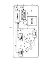
図1は、フォトリソグラフィ工程で回路パターンが転写された半導体ウェハに対してマクロ検査を行う基板検査装置1(欠陥検査装置)の構成を示している。基板検査装置1は、図示しない検査対象の基板(半導体ウェハ)が投入されたところで欠陥検査(欠陥検出、欠陥分類、基板を構成するチップ及び基板全体の良否判定等)を行い、検査結果として生成される検査結果情報を出力する。
FIG. 1 shows a configuration of a substrate inspection apparatus 1 (defect inspection apparatus) that performs a macro inspection on a semiconductor wafer to which a circuit pattern is transferred in a photolithography process. The
マクロ検査を行う際には、まず、基板に対して傾きを持った状態で照明光を当て、その反射光を1次元のラインセンサで受光することで画像情報を得る。具体的には、ステージ等のような基板搬送系又は撮像系を「相対的に」移動させながら、ラインセンサから逐次取得される1次元の画像情報を並べて2次元の「画像情報」を生成する。そして、2次元の画像情報に対して欠陥検査を行う。 When performing a macro inspection, first, illumination light is applied with the substrate tilted, and the reflected light is received by a one-dimensional line sensor to obtain image information. Specifically, two-dimensional “image information” is generated by arranging the one-dimensional image information sequentially acquired from the line sensor while moving the substrate transport system or imaging system such as a stage “relatively”. . Then, defect inspection is performed on the two-dimensional image information.
この欠陥検査は次のような情報伝達によって行われる。装置制御部11は、基板検査装置1の内部制御を行う機能を有しており、まず、検査対象の基板が基板検査装置1に投入される旨の情報を含む制御情報aaを装置制御部11が受け取る。制御情報aaは、例えば半導体ウェハの製造工程全体を管理している製造工程管理装置(図示せず)から出力される。
This defect inspection is performed by the following information transmission. The
装置制御部11は、制御情報aaを受け取ったところで、照明系制御部13、撮像センサ制御部14、及びステージ制御部17に対して、基板投入のための準備を行う指示を出す。装置制御部11は、照明系制御部13とは照明制御情報cc、撮像センサ制御部14とは撮像センサ制御情報dd、ステージ制御部17とはステージ制御情報eeという双方向の情報を取り扱う。これらの各制御部は基板の欠陥検査の準備を行い、「検査準備完了」の旨を示す情報を装置制御部11に送る。
Upon receiving the control information aa, the
各制御部からの「検査準備完了」の通知を受けたところで、装置制御部11は、照明系制御部13、撮像センサ制御部14、及びステージ制御部17に対して、画像情報取得のための処理を行うように指示を出す。具体的には、照明系制御部13が、照明部15に対して、照明情報ffによって照明光量等を指定して基板に照明光を当てるようにする。また、ステージ制御部17が、検査ステージ18に対してステージ駆動情報hhを出力することで、検査対象の基板が搭載された検査ステージ18を、撮像センサ16の画素が並ぶ1次元方向に対して垂直な方向に駆動するようにする。ステージ駆動情報hhには、駆動時の初速度、加速度、及び到達速度等の情報が含まれる。
Upon receiving the notification of “inspection preparation completion” from each control unit, the
そして、撮像センサ制御部14は、撮像情報ggによって撮像センサ16に対して撮像を指示し、1ライン分の画像情報を生成させる。撮像情報ggには、撮像時の露光時間やゲイン、ライン転送のタイミング等の情報が含まれる。撮像センサ16によって取得された1ライン分の画像情報は、ライン画像情報kkとして、本発明の主要部分である画像処理部19に送られる。
Then, the imaging
画像情報の取得が行われる一方で、製造工程/品種情報取得部12は、「検査に必要な情報」として、現在の検査対象に関する情報、例えば製造工程や品種といった情報を含む検査対象情報bbを製造工程管理装置から受け取る。製造工程/品種情報取得部12は、検査対象情報bbを以降の欠陥検査で活用できる情報に変換する処理、例えば品種に関する情報を半導体ウェハの設計情報(ウェハのチップやショットの大きさ、間隔、縦/横方向の配置位置等)に変換する処理を行う。変換された情報は、検査用製造工程/品種情報mmとして、画像処理部19に送られる。
While the image information is acquired, the manufacturing process / product
画像処理部19は、ライン画像情報kkの取得/記憶が完了したことを認識すると、画像記憶制御情報nnとして「画像情報取得完了」の旨の情報を装置制御部11に送る。装置制御部11はその情報を受け取ると、照明系制御部13、撮像センサ制御部14、ステージ制御部17に画像取得完了の旨の制御情報を出力し、画像取得のための動作を完了させる。
When the
そして、装置制御部11は、「画像検査開始」の旨の情報を画像記憶制御情報nnとして画像処理部19に送る。画像処理部19は、後述する処理を行って検査結果情報ppを出力する。検査結果情報ppが製造工程管理装置に送られることで、製造工程管理装置は、検査ステージ18上にある基板の検査が終了したことを認識し、基板の排出等といった検査終了のための処理を基板検査装置1に指示する。
Then, the
次に、図2を参照し、画像処理部19の構成及び動作を説明する。画像取込部21は、ライン画像情報kkの取得/記憶を行い、撮像が完了した(既定されているライン数分の画像情報の取得/記憶を完了した)ところで、「画像情報取得完了」の旨を示す画像記憶制御情報nnを装置制御部11に送る。続いて、「画像検査開始」の旨を示す画像記憶制御情報nnを装置制御部11から受け取ったところで、検査処理が開始される。
Next, the configuration and operation of the
このとき、画像取込部21は各ラインの画像情報を組み合わせて、検査基板に関する2次元の画像情報を生成する。なお、画像取込部21は、ライン画像情報kkに対して、ノイズ除去処理や、明るさを補正するシェーディング補正、幾何学的な歪みを補正するディストーション補正といった、撮像系の補正に関する画像処理も行う。
At this time, the
画像取込部21によって生成された2次元画像情報は、2次元画像情報rrとしてDWT処理部22に送られる。DWT処理部22は、後述する離散ウェーブレット変換(Discrete Wavelet Transform;以下DWT)により、画像のスケール(画像サイズ、言い換えると画像を構成する画素の数)が縮小された縮小スケール画像情報ssを生成して出力する。縮小スケール画像情報ssには、1つの画像を形成する情報に限らず、周波数成分に応じて複数の画像を形成する情報が含まれる。
The 2D image information generated by the
DWT処理部22から出力された縮小スケール画像情報ssは、検査用周波数画像選択部23に送られる。検査用周波数画像選択部23は、画像を構成する縮小スケール画像情報ssに対して、以降の処理を行うか、それともスケールの縮小を再度行うかを判断し、必要な画像情報を選択する。選択の基準については、製造工程/品種情報取得部12から出力される検査用製造工程/品種情報mmの中に、以降の処理を行う対象となる次数(ここではDWT処理により縮小された回数を表す)の周波数成分が1つ以上設定されており、その設定内容に基づいて画像情報が選択される。
The reduced scale image information ss output from the
上記のようにして選択された画像情報は選択画像情報ttとして出力される。なお、選択画像情報ttは1つの画像情報に限らない。また、選択画像情報ttの対象が、以降の処理で再度DWT処理部22に送られる画像情報なのか、又は検査対象となる画像情報なのかを区別できるようにする。以降の処理を表す情報は、スイッチ切替情報uuとして出力される。
The image information selected as described above is output as selected image information tt. The selected image information tt is not limited to one image information. In addition, it is possible to distinguish whether the target of the selected image information tt is image information sent again to the
スイッチ24は、スイッチ切替情報uuを受け取り、選択画像情報ttの送り先を決定する。スイッチ切替情報uuの内容が再度DWT処理部22での処理を指示するものであれば、スイッチ24は、選択画像情報ttを縮小2次元画像情報yyとして再度DWT処理部22に送るように出力先を切り替える。DWT処理部22は、縮小2次元画像情報yyの入力を受けて、縮小2次元画像情報yyに対して再度DWT処理を行う。一方、スイッチ切替情報uuの内容が欠陥検査処理の開始を指示するものであれば、スイッチ24は、選択画像情報ttを検査対象画像情報wwとして欠陥検出部25に送るように出力先を切り替える。
The
欠陥検出部25は、検査対象画像情報wwに対して、欠陥検出処理を行う。欠陥検出部25には、製造工程/品種情報取得部12から出力される検査用製造工程/品種情報mmも入力される。ここで、検査用製造工程/品種情報mmには、検査対象の半導体ウェハに関する設計情報(例えばチップ/ダイの大きさ、隣接するチップ/ダイの間隔、チップ/ダイの個数、複数のチップ/ダイからなるショットの個数、ウェハの直径等)や、事前の検査条件(レシピ)設定時に欠陥検出用に登録された参照用画像情報(欠陥のない検査対象物を撮像した画像の情報)、ウェハを識別するためのID番号等が含まれる。
The
特に、参照用画像情報については、適切な欠陥検出ができるように、検査対象画像情報wwと同じ次数(画像のスケールが同じ)、同じ周波数成分となっている。本実施形態では、参照用画像情報と検査対象画像情報wwとを比較して、異なる箇所を欠陥として検出する公知の方法をとっている。欠陥検出処理の結果は、欠陥検出情報xxとして出力される。欠陥検出情報xxには、検査対象画像情報ww内における欠陥の有無、欠陥が存在する場合の欠陥の画像上の位置、面積、フェレ径(欠陥の外接矩形の幅/高さ)、周囲長(欠陥の輪郭線の長さ)、真円度(欠陥の形状の複雑さを円と比較して表される数値)等が含まれる。 In particular, the reference image information has the same order (same image scale) and the same frequency component as the inspection target image information ww so that appropriate defect detection can be performed. In the present embodiment, a known method is used in which the reference image information and the inspection target image information ww are compared and a different portion is detected as a defect. The result of the defect detection process is output as defect detection information xx. The defect detection information xx includes the presence / absence of a defect in the inspection object image information ww, the position of the defect on the image, the area, the ferret diameter (width / height of the circumscribed rectangle of the defect), the perimeter ( The length of the outline of the defect), the roundness (a numerical value expressed by comparing the complexity of the defect shape with the circle), and the like.
欠陥分類/判定部26は、欠陥検出部25から出力される欠陥検出情報xx、画像取込部21から出力される2次元画像情報rr、及び製造工程/品種情報取得部12から出力される検査用製造工程/品種情報mmの入力を受けて、検出された欠陥の分類、及び検査対象に関する良品/不良品判定を行う。欠陥分類処理では、欠陥検出情報xxに加えて、検査の元画像の情報である2次元画像情報rrが用いられる。即ち、欠陥検出情報xxで欠陥があると該当する箇所について、2次元画像情報rrを用いて、より詳細に分析を行い、的確な分類を行うようにする。
The defect classification /
本実施形態における欠陥分類処理は、分類内容を決めるためのルール(予め記憶されているもの)に基づき、欠陥の特徴量(欠陥検出情報xxが示す特徴量だけでなく、2次元画像情報rrのうち、欠陥に該当する箇所から算出する特徴量も含む)から各ルールの適合度を算出し、適合度が最大となるルールの分類を適用するというものである。このルールは、例えば「キズ」という分類を表す特徴として、欠陥の面積とフェレ径を用い、面積が小さい、且つフェレ径が細長い(一方の径の長さが他方に対して長い)場合に「キズ」であるという内容を数値化したものである。欠陥の面積が小さいほど、且つフェレ径が細長い(縦及び横のフェレ径の比が1に比べて大きく又は小さくなる)ほど、「キズ」の適合度は大きくなる。 The defect classification processing in this embodiment is based on the rule for determining the classification contents (those stored in advance), not only the defect feature amount (not only the feature amount indicated by the defect detection information xx) but also the two-dimensional image information rr. Among them, the matching degree of each rule is calculated from the feature amount calculated from the location corresponding to the defect), and the classification of the rule that maximizes the matching degree is applied. This rule uses, for example, a defect area and a ferret diameter as a feature representing a classification “scratch”, and when the area is small and the ferret diameter is long (one diameter is longer than the other), The content of “scratches” is quantified. The smaller the defect area and the longer the ferret diameter (the ratio of the vertical and horizontal ferret diameters is larger or smaller than 1), the greater the degree of conformity of “scratches”.
分類処理はこの方法にとどまらず、例えば特開2003−168114号公報に開示されている内容(分類処理の内部において、ある欠陥に対して分類種別が確定したものを欠陥情報から除外して分類精度を向上させる方法であり、ファジイ推論を用いて分類ルールを適用している)等のようなものを利用してもよい。決定される分類内容は1つに限らず、適合度に応じて複数存在してもよい。なお、分類内容を決めるためのルールは、検査の内容や基板の経時変化に対応するため、更新(新規ルールの追加、既存ルールの修正、削除)が可能である。 The classification process is not limited to this method. For example, the contents disclosed in Japanese Patent Application Laid-Open No. 2003-168114 (the classification accuracy is determined by excluding those in which the classification type is determined for a certain defect from the defect information. And the like (which applies a classification rule using fuzzy inference) may be used. The number of classification contents to be determined is not limited to one, and a plurality of classification contents may exist depending on the degree of fitness. It should be noted that the rules for determining the classification contents can be updated (adding new rules, modifying or deleting existing rules) in order to cope with the contents of inspection and changes with time of the board.
また、検査対象物に関する良品/不良品判定処理は、欠陥検出情報xxや、直前に決定された分類内容、検査用製造工程/品種情報mmの中に含まれているウェハ設計情報等に基づき、各チップ/ダイに関する良品/不良品の判定、及び検査基板であるウェハとしての良品/不良品の判定を行うものである。 In addition, the non-defective / defective product determination process for the inspection object is based on the defect detection information xx, the classification content determined immediately before, the wafer design information included in the manufacturing process / product information mm for inspection, etc. The non-defective product / defective product for each chip / die is determined, and the non-defective product / defective product as the inspection substrate is determined.
各チップ/ダイに関しては、欠陥の有無に従って、又は欠陥があった場合は特徴量や分類内容等から予め設定された良品/不良品を区別するための条件(閾値等)に従って判定が行われる。条件は、例えばあるチップ/ダイに関して、欠陥面積がチップ/ダイのサイズの20%以上である、又は分類内容がチップ/ダイの機能上致命的なもの(ショットデフォーカス等)である場合にそのチップ/ダイを不良品とする等といったものである。この判定によって、予め設定された検査領域であるチップ/ダイに対する以降の処理の可否が決定される。 Each chip / die is determined according to the presence / absence of a defect, or when there is a defect, according to a condition (threshold value, etc.) for discriminating a good / defective product set in advance from a feature amount, classification content, or the like. The condition is, for example, when the defect area is 20% or more of the chip / die size or the classification content is critical to the function of the chip / die (such as shot defocus). For example, the chip / die is regarded as a defective product. By this determination, whether or not the subsequent processing is possible for the chip / die which is a preset inspection region is determined.
また、ウェハに関しては、各チップ/ダイの判定結果を踏まえ、不良品と判定されたチップ/ダイが、予め設定された条件、例えば全チップ/ダイの10%以上であれば不良品、そうでなければ良品と判定する等のような条件に従って判定が行われる。この判定によって、検査対象物であるウェハに対する以降の処理の可否が決定される。 In addition, regarding the wafer, based on the determination result of each chip / die, if the chip / die determined to be defective is a preset condition, for example, 10% or more of all chips / dies, it is defective. If not, the determination is made according to a condition such as determining a non-defective product. Based on this determination, whether or not a subsequent process can be performed on the wafer that is the inspection object is determined.
図3は、チップ/ダイに関する判定の様子を示している。図3(a)は、検査対象であるウェハ31aを撮像して得たウェハ画像情報31の画像を示しており、チップ/ダイ32が32個配置されている。ウェハ31aの直径は300mmであり、チップ/ダイ32のサイズは縦40mm×横40mmである。
FIG. 3 shows a state of determination regarding the chip / die. FIG. 3A shows an image of
ウェハ31a上には3個の欠陥33a,33b,33cが存在する。このうち、欠陥33aは6個のチップ/ダイに跨っており、それらのうち4個のチップ/ダイの大部分は欠陥で埋められている。前述したチップ/ダイの良品/不良品の判定条件(欠陥面積がチップ/ダイのサイズの20%以上なら不良品)に従うと、大部分が欠陥で埋められている4個のチップ/ダイは不良品として判定される。
There are three
一方、欠陥33aがわずかにかかっているチップ/ダイ、及び欠陥33b,33cがあるチップ/ダイは、欠陥の面積が小さいことから、前述した良品/不良品の判定条件に従うと、良品として判定される。図3(b)のチップ/ダイ判定結果マップ34は各チップ/ダイの良品/不良品の判定結果を示している。チップ/ダイ判定結果マップ34では、各チップ/ダイについて、良品判定が“○”、不良品判定が“×”として示されている。
On the other hand, a chip / die having a
また、チップ/ダイの判定結果を統合することで、ウェハ31aに関する良品/不良品の判定を行うことができる。前述したウェハの良品/不良品の判定条件(全チップ/ダイの10%以上なら不良品)に従うと、32個中4個のチップ/ダイが不良品である、即ち不良品の割合が12.5%であることから、ウェハ31aは不良品として判定される。
Further, by integrating the chip / die determination results, it is possible to determine whether the
欠陥分類/判定部26での欠陥分類/判定処理が終了すると、検査結果情報ppが生成され、欠陥分類/判定部26から出力される。検査結果情報ppには、検査結果に関するあらゆる情報が含まれる。それには、欠陥の特徴に関する欠陥検出情報xxや、分類/判定結果だけでなく、検査時間や検査装置の固有ID、検査用製造工程/品種情報mmから取得されたウェハ識別ID番号(検査された基板(ウェハ)の固有ID)等も含まれる。
When the defect classification / determination process in the defect classification /
図4は、図3のウェハ31aに関する検査結果情報ppの内容のフォーマットを示している。図4では、基板検査に共通した項目として、検査終了時間、検査装置ID、ウェハID、欠陥数、及びウェハ判定結果が設定されている。また、各欠陥に関する情報として、欠陥位置、欠陥面積、欠陥のフェレ径、欠陥の分類内容、分類内容の適合度、欠陥に該当するチップ/ダイの位置(Index)、及びチップ/ダイの判定結果が欠陥数に応じて設定されている。
FIG. 4 shows the format of the contents of the inspection result information pp related to the
ここで、欠陥位置及びチップ/ダイの位置(Index)は夫々、左上を原点とした座標系で示されている。図4のフォーマットの表記では、1行が1個の欠陥に関連する情報としているが、例えば図3の欠陥33aのように、複数のチップ/ダイに跨っている欠陥に関しては、欠陥33aがあるチップ/ダイの位置、及び夫々の判定結果を別の行として表す(一方で重複する情報は出さない)ようにする。また、欠陥33cのように、分類内容が複数(「該当無」という内容の適合度が最も大きい)存在する場合も同様に、夫々の分類内容を別の行として表すようにする。
Here, the defect position and the chip / die position (Index) are shown in a coordinate system with the upper left as the origin. In the notation of the format of FIG. 4, one row is information related to one defect, but there is a
次に、本実施形態による基板検査装置1の詳細な動作手順を説明する。図5は基板検査装置1の内部及び画像処理部19の内部の処理手順を示している。図5が示す処理は、既に基板が基板検査装置1に搬入された状態から、検査の終了した基板が基板検査装置1から搬出される直前までに行われる処理である。
Next, a detailed operation procedure of the
まず、装置制御部11の指示(検査準備指示)により、照明系、撮像系、及びステージが検査可能な状態になる(ステップS11)。照明系、撮像系、及びステージが検査準備完了(検査可能な状態)となったことを受け、装置制御部11は、検査対象となる検査基板を検査ステージ18に配置し、検査ステージ18を平面方向(撮像センサ16の画素が並ぶ1次元方向に対して垂直な方向)に駆動しながら、検査画像情報を取得する制御を行う(ステップS12)。
First, according to an instruction (inspection preparation instruction) from the
検査基板であるウェハ全体の撮像が完了した(画像処理部19に撮像センサ16からの画像情報が送られた)ことが装置制御部11に通知されると、装置制御部11からの指示により、画像取込部21は2次元画像情報rrを生成する(ステップS13)。続いて、DWT処理部22は2次元画像情報rr(又は縮小された縮小2次元画像情報yy)を受け取ってDWT処理を行い、予め指示された周波数成分をもつ1以上の縮小スケール画像情報ssを生成する(ステップS14)。
When the
検査用周波数画像選択部23は縮小スケール画像情報ssを受け取り、その中から、以降の処理で利用する縮小スケール画像情報を選択し、選択画像情報ttとして出力する(ステップS15)。スイッチ24は、選択画像情報ttとして出力された縮小スケール画像情報に関して、欠陥検査の対象であるか否かを調べる(ステップS16)。縮小スケール画像情報が欠陥検査の対象であれば(ステップS16でYesの場合)ステップS18へ、そうでなければ(ステップS16でNoの場合)ステップS17へ夫々進む。
The inspection frequency
ステップS16において、縮小スケール画像情報が欠陥検査の対象でなかった場合、ステップS16での判定対象となった選択画像情報ttに対してDWT処理が適用できるように、スイッチ24は選択画像情報ttを縮小2次元画像情報yyとして設定する(ステップS17)。この後、ステップS14に進み、縮小2次元画像情報yyに対するDWT処理が行われる。
In step S16, if the reduced scale image information is not the object of defect inspection, the
また、ステップS16において、縮小スケール画像情報が欠陥検査の対象であった場合、スイッチ24は、装置制御部11からの指示に従い、縮小スケール画像情報を検査対象画像情報wwとする。欠陥検出部25は、検査対象画像情報wwと同じ次数(DWT処理の実行回数及び縮小スケールが同一)、同じ周波数成分からなる参照画像情報を用いて、検査対象画像情報wwに関する欠陥検出処理を行い、欠陥検出情報xxを生成する(ステップS18)。
In step S16, if the reduced scale image information is a defect inspection target, the
欠陥分類/判定部26は、欠陥検出処理にて検出された欠陥に関して、ステップS18で生成された欠陥検出情報xxと共に元の2次元画像情報rrを用いて欠陥分類処理を行う(ステップS19)。 更に、欠陥分類/判定部26は、欠陥検出情報xxや2次元画像情報rr、及びステップS19で得られた欠陥の特徴量情報や欠陥分類結果等を利用して、チップ/ダイの単位及びウェハの単位に関する良品/不良品の判定処理を行う(ステップS20)。
The defect classification /
良品/不良品の判定処理の終了後、これまで生成された欠陥に関する各種情報(特徴量、分類結果、良品/不良品の判定結果)の他に、検査時間や検査装置のID、検査基板であるウェハのID等の検査情報を加えて、欠陥分類/判定部26は、図4に示すフォーマットに従った検査結果情報ppを生成する(ステップS21)。最後に、欠陥分類/判定部26から検査結果情報ppが出力されて製造工程管理装置に送信され、基板検査の終了処理(基板搬出のための準備等)が行われる(ステップS22)。図5の処理は1枚の検査基板に関するものであり、これを繰り返すことで逐次基板を検査することとなる。
After the non-defective / defective product judgment process, in addition to various information (features, classification results, good / defective product judgment results) related to the defects generated so far, the inspection time, inspection device ID, and inspection board In addition to inspection information such as an ID of a wafer, the defect classification /
次に、DWT処理部22が行う処理の詳細を説明する。DWT処理部22は、離散ウェーブレット変換(DWT)による画像の多重解像度解析を行う。図6は、図3に示したウェハ画像情報31(3個の欠陥が存在するウェハ31aを撮像したもの)を対象とした例を示している。離散ウェーブレット変換による画像の多重解像度解析とは、元の画像情報を、低周波成分画像情報、水平方向の高周波成分画像情報、垂直方向の高周波成分画像情報、対角方向の高周波成分画像情報という、周波数成分の異なる4種類の縮小スケール画像情報に変換する方法である。
Next, details of processing performed by the
生成された縮小スケール画像情報を更に多重解像度解析に適用することが可能である。更に、変換された各周波数成分の縮小スケール画像情報から変換前の画像情報を完全に復元する可逆変換も可能である。多重解像度解析は、画像の次元をそのままにして解像度を変換できることからピラミッドアルゴリズムとも呼ばれ、JPEG2000の画像圧縮技術に利用されている。 The generated reduced scale image information can be further applied to multiresolution analysis. Furthermore, reversible conversion that completely restores image information before conversion from the reduced scale image information of each converted frequency component is also possible. Multi-resolution analysis is also called a pyramid algorithm because it can convert the resolution without changing the dimension of the image, and is used in JPEG 2000 image compression technology.
ウェハ画像情報31に対して、離散ウェーブレット変換による多重解像度解析を行うと、低周波成分の画像情報31-LL1、水平方向の高周波成分の画像情報31-HL1、垂直成分の高周波成分の画像情報31-LH1、対角成分の高周波成分の画像情報31-HH1という4種類の画像情報が生成される。変換前後の画像の様子を図7に示す。変換後の画像はいずれも、画像のスケールに関して、元の画像に対して幅、高さが共に1/2となっており、1次の周波数成分画像と位置づけられる。
When multi-resolution analysis is performed on the
画像情報31-HL1は、水平方向の高周波数成分であるから、水平方向にコントラストの強い箇所が明るくなり、画像情報31-LH1は、垂直方向の高周波数成分であるから、垂直方向にコントラストの強い箇所が明るくなる。一方、画像情報31-HH1は、対角方向の高周波数成分であるから、例えば矩形図形におけるコーナー(角)のような箇所が明るくなる。 Since the image information 31-HL1 is a high frequency component in the horizontal direction, a portion having a strong contrast in the horizontal direction is brightened, and since the image information 31-LH1 is a high frequency component in the vertical direction, the contrast in the vertical direction is high. Strong areas become brighter. On the other hand, since the image information 31-HH1 is a high frequency component in the diagonal direction, for example, a corner (corner) in a rectangular figure becomes bright.
また、低周波成分の画像情報31-LL1に対して、更に離散ウェーブレット変換による多重解像度解析を行うと、2次の周波数成分画像情報として、低周波成分の画像情報31-LL2、水平方向の高周波成分の画像情報31-HL2、垂直成分の高周波成分の画像情報31-LH2、対角成分の高周波成分の画像情報31-HH2という4種類の縮小スケール画像情報が生成される。 Further, when multi-resolution analysis is performed on the low-frequency component image information 31-LL1 by discrete wavelet transform, the low-frequency component image information 31-LL2 and the horizontal high-frequency component are obtained as secondary frequency component image information. Four types of reduced scale image information are generated: component image information 31-HL2, vertical high-frequency component image information 31-LH2, and diagonal high-frequency component image information 31-HH2.
これらはいずれも、画像のスケールに関して、低周波成分の画像情報31-LL1に対して幅、高さが共に1/2、即ち元の画像に対して幅、高さが共に1/4となる。このとき、低周波成分の画像情報31-LL2では、ウェハ31aの右下に存在する欠陥33bや欠陥33c(元の画像に対して面積が極めて小さい欠陥)の情報が失われ、それらの欠陥を検出できない可能性が出てくる。しかし、水平方向の高周波成分の画像情報31-HL2及び垂直成分の高周波成分の画像情報31-LH2では、それらの欠陥は、検出できる状態で残る可能性が高い。
Both of these are 1/2 in width and height with respect to the image information 31-LL1 of the low frequency component in terms of the image scale, that is, both the width and height are 1/4 with respect to the original image. . At this time, in the image information 31-LL2 of the low frequency component, information on the
図8は、上述した多重解像度解析により生成された周波数成分ごとの縮小スケール画像情報を利用した画像比較による欠陥検出例を示している。ここでは、欠陥検出に用いる参照画像情報41も、事前の検査条件(レシピ)設定において、上述した方法に基づいて、縮小スケール画像情報として生成されている。即ち、1次の周波数成分画像を欠陥検出に用いる場合には、参照画像情報として低周波成分の画像情報41-LL1、水平方向の高周波成分の画像情報41-HL1、垂直成分の高周波成分の画像情報41-LH1、対角成分の高周波成分の画像情報41-HH1という4種類の縮小スケール画像情報のうち1つ以上が保持されることになる。
FIG. 8 shows an example of defect detection by image comparison using reduced scale image information for each frequency component generated by the multiresolution analysis described above. Here, the
ウェハ画像情報31に対しても、参照画像情報と同じ次数の周波数成分画像(画像情報31-LL1,31-HL1,31-LH1,31-HH1)が生成される。そして、参照画像情報との位置合わせ(マッチング)が行われた後、参照画像情報と同一の周波数成分をもつ画像同士が比較される。すると、欠陥検出結果として、低周波成分の画像情報51-LL1、水平方向の高周波成分の画像情報51-HL1、垂直成分の高周波成分の画像情報51-LH1、対角成分の高周波成分の画像情報51-HH1という4種類の結果が得られる(実際には参照画像情報として保持している周波数成分に関して得られる)。全ての周波数成分を利用すると、処理時間は元の画像同士の比較とさほど変わらないが、例えば水平と垂直の高周波成分について調べる、又は1次の低周波成分から2次の周波数成分を生成して用いる等とすれば、欠陥検出の処理時間を大幅に削減することが可能である。
Also for the
図8に示すように、欠陥31aと同様に欠陥33bや欠陥33cも検出可能である。しかし、欠陥33cよりも更に微小な欠陥の場合、低周波成分では検出できないことも十分考えられる。また、図6に示した2次の周波数成分を利用しようとすると、低周波成分では欠陥31cが見られないことから、欠陥を見落とす可能性がある。一方、高周波成分では欠陥全体というより、欠陥と思われる箇所の「輪郭」を検出することになる。これは、2次の周波数成分を利用する場合でも同様である。
As shown in FIG. 8, the
ここに本実施形態の特徴として、欠陥検出については、できるだけ少ない情報を用いることで「欠陥として疑いのありそうな箇所」を見つけることに徹し、欠陥の検出された箇所については、元の画像情報を利用して、「本当に欠陥なのか?欠陥だとしたらどういった特徴をもち、どの種類になるのか?」を詳細に調べるようにしている。特徴量の算出や分類という処理は、欠陥が存在するときに行われるものであるが、欠陥検出は全ての検査対象物に対して実行されるため、この時間を短縮することが検査時間のスループットに反映される。 Here, as a feature of the present embodiment, with regard to defect detection, by using as little information as possible, it is devoted to finding a “possibly suspected defect”, and for the detected defect, the original image information Is used to investigate in detail, "What is it really a defect? If it is a defect, what are the characteristics and what type?" The process of calculating and classifying feature amounts is performed when a defect exists, but defect detection is performed for all inspection objects, so reducing this time can reduce the inspection time throughput. It is reflected in.
上述したように、本実施形態では、離散ウェーブレット変換に基づく多重解像度解析を利用し、元の画像情報に対応した画像よりも画像サイズ(画像のスケール)を縮小した縮小スケール画像情報を生成する。そして、縮小スケール画像情報と比較対象の参照用の縮小スケール画像情報の比較によって欠陥検出を行うことにより、元の2次元画像情報に対して欠陥検査を行う場合に比べ、検査時間を削減し、高速に欠陥検査を行うことができる。また、分解能の小さい高精細な画像情報を用いた欠陥検査であっても、コストを要する複雑なシステム構成が不要であり、コストの増大を抑えることができる。 As described above, in the present embodiment, reduced-scale image information in which the image size (image scale) is reduced as compared with the image corresponding to the original image information is generated by using multiresolution analysis based on discrete wavelet transform. Then, by performing defect detection by comparing the reduced scale image information with the reference reduced scale image information for comparison, the inspection time can be reduced as compared with the case of performing defect inspection on the original two-dimensional image information, Defect inspection can be performed at high speed. In addition, even for defect inspection using high-definition image information with low resolution, a complicated system configuration that requires cost is unnecessary, and an increase in cost can be suppressed.
また、2次元画像情報の周波数成分に着目して複数の縮小スケール画像情報を生成するため、例えば異物やキズといった高周波成分の強い欠陥に関する情報と、膜のムラといった低周波成分の強い欠陥に関する情報とを、それぞれ別々の縮小スケール画像情報として得ることができる。更に、縮小スケール画像情報が周波数成分に依存したものであることから、元の2次元画像情報を用いて欠陥検査を行う場合と同等の「質」(=欠陥検出能力)を維持することができる。 In addition, in order to generate a plurality of reduced scale image information by paying attention to the frequency component of the two-dimensional image information, for example, information on a defect having a high frequency component such as a foreign object or a scratch, and information on a defect having a strong low frequency component such as film unevenness Can be obtained as separate reduced-scale image information. Furthermore, since the reduced scale image information depends on the frequency component, the “quality” (= defect detection capability) equivalent to that when performing defect inspection using the original two-dimensional image information can be maintained. .
また、多重解像度解析は、本実施形態で説明した離散ウェーブレット変換に代表される解析方法であり、画像情報を高周波成分と低周波成分に分解し、得られた高周波成分又は低周波成分を更に高周波成分と低周波成分に分解するというように、情報を高周波成分と低周波成分に分解する処理を繰返し行うものである。これにより、高周波成分及び低周波成分の観点で分割された縮小スケール画像情報を得ることができる。また、繰り返して周波数成分の分解が可能であることから、スケールがより縮小された縮小スケール画像情報を得ることができ、検査時間をより削減することができる。 The multi-resolution analysis is an analysis method represented by the discrete wavelet transform described in the present embodiment. The image information is decomposed into a high-frequency component and a low-frequency component, and the obtained high-frequency component or low-frequency component is further converted into a high-frequency component. A process of resolving information into a high frequency component and a low frequency component is repeatedly performed, such as decomposing into a component and a low frequency component. Thereby, the reduced scale image information divided | segmented from the viewpoint of the high frequency component and the low frequency component can be obtained. Further, since the frequency component can be repeatedly decomposed, it is possible to obtain reduced scale image information with a further reduced scale, thereby further reducing the inspection time.
また、本実施形態では、欠陥検査で利用する検査対象物の縮小スケール画像情報と同一の方法で参照画像情報(欠陥のない検査対象物を撮像したもの)が生成され、両者の解像度が同一になる。これによって、スケールが縮小された状態であっても、元の画像情報を利用したときと同等の欠陥検出精度及び確度を維持した欠陥検査を行うことができる。 Further, in the present embodiment, reference image information (captured inspection object having no defect) is generated by the same method as the reduced scale image information of the inspection object used in defect inspection, and the resolution of both is the same. Become. As a result, even when the scale is reduced, it is possible to perform a defect inspection that maintains the same defect detection accuracy and accuracy as when the original image information was used.
また、欠陥検査で検出された欠陥に関する特徴量や、欠陥がどういったものかを表す分類結果、検査領域及び検査対象物に関する良否判定結果を検査結果情報とすることで、詳細な欠陥検査を行うことができる。 In addition, detailed defect inspection can be performed by making the inspection result information the feature amount related to the defect detected in the defect inspection, the classification result indicating what the defect is, and the pass / fail judgment result regarding the inspection area and inspection object. It can be carried out.
また、本実施形態では、DWT処理部22の1回のDWT処理により、4種類の縮小スケール画像情報が生成される。欠陥検出部25が、検査対象物上の欠陥を抽出する処理を、各々の縮小スケール画像情報に対して個別に行う場合には、周波数成分別に生成された各縮小スケール画像情報を用いて欠陥検査を行うことにより、キズや異物といった高周波成分の欠陥に関する検査と、膜ムラのような低周波成分の欠陥に関する検査とを別々の処理系で行うことができ、縮小スケール画像情報がもつ周波数成分の情報に特化した検査結果情報を得ることができる。
In the present embodiment, four types of reduced scale image information are generated by one DWT process of the
(第2の実施形態)
次に、本発明の第2の実施形態を説明する。以下、第1の実施形態と異なる箇所のみを記述する。図9は、本実施形態による基板検査装置1内の画像処理部19の構成を示している。第1の実施形態(図2)と異なる箇所は、DWT処理部22に代わって濃淡モフォロジー処理部61を設けていることである。
(Second Embodiment)
Next, a second embodiment of the present invention will be described. Hereinafter, only different points from the first embodiment will be described. FIG. 9 shows the configuration of the
濃淡モフォロジー処理部61は、2次元画像情報rrに対して、後述する濃淡モフォロジー処理を行い、処理結果を検査対象画像情報wwとして出力する。2次元画像情報rrと共に入力される検査用製造工程/品種情報mmには、予め検査条件として設定された、モフォロジー演算に関する設定(膨張/収縮の演算回数、処理後に出力すべき情報等)が含まれる。
The light and shade
以下、本実施形態における濃淡モフォロジー処理を説明する。図10は、1次元の画像情報を対象とした濃淡モフォロジー処理を表しており、図10(a)の原画像情報が明暗の情報を持つ。例えば、モフォロジー演算におけるフィルタのサイズを3画素とすると、Dilation(膨張)は各画素に関してフィルタ内の3画素の中で最大輝度に置換する演算であり、Erosion(収縮)は同様にフィルタ内の3画素の中で最小輝度に置換する演算である。 Hereinafter, the light and shade morphology process in this embodiment will be described. FIG. 10 shows a light and shade morphology process for one-dimensional image information, and the original image information in FIG. 10A has light and dark information. For example, if the size of the filter in the morphological operation is 3 pixels, Dilation is an operation that replaces each pixel with the maximum luminance among the 3 pixels in the filter, and Erosion is similarly 3 in the filter. This is an operation for replacing the pixel with the minimum luminance.
モフォロジー演算を繰り返すことで、膨張/収縮の効果が大きくなる。例えばモフォロジー演算回数を3回とした場合、図10(a)に対するDilation(膨張)演算の結果は図10(b)のようになり、明部の情報が広がると同時に暗部の情報が消失する。同様にErosion(収縮)演算の結果は図10(c)のようになり、暗部の情報が広がると同時に明部の情報が消失する。 By repeating the morphological operation, the effect of expansion / contraction increases. For example, when the number of morphological operations is 3, the result of the Dilation operation with respect to FIG. 10A is as shown in FIG. 10B, and the information in the dark portion disappears at the same time as the bright portion information spreads. Similarly, the result of the erosion (shrinkage) calculation is as shown in FIG. 10C, and the information on the dark part spreads and the information on the bright part disappears.
図10(a)〜(c)の情報に対して、1/2に縮小するスケール変換を行うと、夫々図10(d)〜(f)のようになる。図10(a)の情報は図10(d)のようになり、明部・暗部ともに情報がスケールの縮小によって消失してしまう。一方、図10(b)の情報は図10(e)のようになり、明部が維持された情報となる。また、図10(c)の情報は図10(f)のようになり、暗部が維持された情報となる。即ち、図10(e)、図10(f)の情報を用いることで、元の画像のコントラストを維持した縮小スケール画像情報を生成することができる。 When the scale conversion for reducing the information of FIGS. 10A to 10C to 1/2 is performed, the information is as shown in FIGS. 10D to 10F, respectively. The information in FIG. 10 (a) is as shown in FIG. 10 (d), and the information disappears due to the reduction in scale in both the bright and dark portions. On the other hand, the information in FIG. 10B is as shown in FIG. 10E, and is information in which the bright portion is maintained. Further, the information in FIG. 10C is as shown in FIG. 10F, and is information in which the dark part is maintained. That is, by using the information shown in FIGS. 10E and 10F, it is possible to generate reduced scale image information that maintains the contrast of the original image.
図11〜図13は、ウェハを撮像して得た2次元画像情報(ウェハ画像情報)に図10と同様の演算を適用したものである。図11(a)の画像情報に対して、1/2に縮小するスケール変換を行うと、図11(b)のようになる。図11(a)と図11(b)を比較すると、白欠陥65aは辛うじて残っているが、小さな黒欠陥65bは消失してしまっている。
11 to 13 are obtained by applying the same calculation as in FIG. 10 to two-dimensional image information (wafer image information) obtained by imaging a wafer. When the scale conversion for reducing the image information of FIG. 11A to 1/2 is performed, the image information is as shown in FIG. Comparing FIG. 11 (a) and FIG. 11 (b), the
一方、図12(a)の画像情報(図11(a)の画像情報に対してDilation(膨張)演算を行ったもの)に対して、1/2に縮小するスケール変換を行うと、図12(b)のようになり、白欠陥66aは、図11(b)の白欠陥65aに比べて十分な大きさを維持している。また、図13(a)の画像情報(図11(a)の画像情報に対してErosion(収縮)演算を行ったもの)に対して、1/2に縮小するスケール変換を行うと、図13(b)のようになり、図11(b)では消失してしまった小さな黒欠陥67bが維持されている。図12(b)と図13(b)の画像情報を用いることで、元の画像情報(図11(a))に比べて情報量を1/2に削減しつつ、コントラストを元の画像と同じ状態に維持できる。
On the other hand, when scale conversion which reduces to 1/2 is performed on the image information in FIG. 12A (the image information in FIG. 11A subjected to Dilation operation), FIG. As shown in FIG. 11B, the
次に、本実施形態による基板検査装置1の詳細な動作手順を説明する。図14は、本実施形態による基板検査装置1の内部及び画像処理部19の内部の処理手順を示している。ステップS31〜S33及びステップS37〜S40は、図5に示したステップS11〜S13及びステップS19〜S22と同等であるので、それらのステップの説明を省略する。
Next, a detailed operation procedure of the
濃淡モフォロジー処理部61は、画像取込部21で生成された2次元画像情報rrに対して、検査用製造工程/品種情報mmで設定されている繰返し回数だけ濃淡モフォロジー演算を行い、中間情報を生成する(ステップS34)。中間情報とは、図12(a)に示すDilation演算結果の情報や、図13(a)に示すErosion演算結果の情報等である。
The light and shade
続いて、濃淡モフォロジー処理部61は、中間情報から、欠陥検査対象となる縮小スケール画像情報を生成し、これを検査対象画像情報wwとして出力する(ステップS35)。欠陥検出部25は、濃淡モフォロジー処理部61から出力された検査対象画像情報wwに対して、装置制御部11からの指示に従って、チップ/ダイ単位の比較に基づく欠陥検出処理を行い、欠陥検出情報xxを生成する(ステップS36)。他の処理は前述した通りである。
Subsequently, the light and shade
なお、図14では、予め設定された繰返し回数だけ濃淡モフォロジー演算が繰り返されて生成された1つの検査対象画像情報wwが欠陥検査の対象となるが、濃淡モフォロジー演算の繰返し回数が異なる複数の検査対象画像情報wwが生成されるようにし、それらが欠陥検査の対象となるようにしてもよい。 In FIG. 14, one inspection target image information ww generated by repeating the density morphological operation for a preset number of repetitions is a target for defect inspection, but a plurality of inspections with different numbers of repetitions of the density morphological operation are performed. The target image information ww may be generated and may be a target for defect inspection.
ここで、チップ/ダイ単位の比較に基づく欠陥検出例を図15に示す。ウェハ画像情報71に対して、検査単位となる検査用チップ/ダイ情報72が生成される。検査用チップ/ダイ情報72は、ウェハ設計情報に基づいてウェハ画像情報71から生成されたものであり、ウェハ画像情報71にある複数のチップ/ダイ領域を取り出し、これらを平均化したチップ/ダイ領域(平均輝度、分散輝度からなる領域)を検査用チップ/ダイ情報72としている。その際、ウェハ画像情報71には欠陥が含まれることが考えられるので、複数のチップ/ダイ領域の平均輝度だけでなく分散輝度も用いるようにする。
Here, FIG. 15 shows an example of defect detection based on chip / die unit comparison. For the
濃淡モフォロジー処理部61によって、ウェハ画像情報71に対して濃淡モフォロジー処理と1/2縮小スケール変換が行われ、欠陥検査用の画像情報(Dilation画像情報73a、Erosion画像情報73b)が生成される。その後、ウェハ上のチップ/ダイだけを検査領域とするように、検査領域の設定(ウェハ設計情報から位置合わせによってチップ/ダイ領域を設定する)が行われ、検査領域画像情報(Dilation画像情報74a、Erosion画像情報74b)が生成される。
The density
生成された検査領域画像情報に対して、自身のチップ/ダイ領域から検査用チップ/ダイ情報72が生成され、欠陥検出部25によって、検査用チップ/ダイ情報72と検査領域画像情報をチップ/ダイ単位で比較する欠陥検出処理が行われ、欠陥検出結果情報75a,75bが生成される。ここで、Dilationからの欠陥検出結果情報75aではウェハ画像情報71の白欠陥76aを白欠陥77aとして、Erosionからの欠陥検出結果情報75bではウェハ画像情報71の微小の黒欠陥76bを黒欠陥77bとして夫々適切に検出できる。
With respect to the generated inspection area image information, inspection chip / die
上述したように、本実施形態では、濃淡モフォロジー演算を利用して、スケールを縮小しても元の2次元画像情報の周波数成分を維持した情報を生成し、これを縮小することで縮小スケール画像情報を生成する。これにより、通常の縮小化(隣接画素の平均化等)では消失するような微小な欠陥が残るような縮小スケール画像情報が得られる。 As described above, in the present embodiment, the reduced-scale image is generated by generating the information that maintains the frequency component of the original two-dimensional image information even if the scale is reduced by using the density morphological operation, and reducing the generated information. Generate information. As a result, reduced scale image information is obtained in which minute defects that remain in normal reduction (such as averaging of adjacent pixels) remain.
この縮小スケール画像情報を用いて欠陥検出を行うことで、元の2次元画像情報に対して欠陥検査を行う場合に比べ、コストの増大を抑えて高速に欠陥検査を行うことができる。また、縮小スケール画像情報が周波数成分に依存したものであることから、元の2次元画像情報を用いて欠陥検査を行う場合と同等の「質」(=欠陥検出能力)を維持することができる。更に、ウェハ自身のチップ/ダイ比較によって欠陥検出を行うことで、参照用の情報を別途用意する必要がない。 By performing defect detection using the reduced-scale image information, it is possible to perform defect inspection at a high speed while suppressing an increase in cost compared to the case of performing defect inspection on the original two-dimensional image information. Further, since the reduced scale image information depends on the frequency component, the “quality” (= defect detection capability) equivalent to the case where defect inspection is performed using the original two-dimensional image information can be maintained. . Furthermore, it is not necessary to separately prepare reference information by performing defect detection by chip / die comparison of the wafer itself.
(第3の実施形態)
次に、本発明の第3の実施形態を説明する。以下、第1、第2の実施形態と異なる箇所のみを記述する。図16は、本実施形態による基板検査装置1内の画像処理部19の構成を示している。第1の実施形態(図2)と異なる箇所は、DWT処理部22に代わって、ブロック分割部81、ブロック対応画素情報決定部82、及びスイッチ83を設けていることである。
(Third embodiment)
Next, a third embodiment of the present invention will be described. Hereinafter, only portions different from the first and second embodiments will be described. FIG. 16 shows the configuration of the
ブロック分割部81は、2次元画像情報rrに対して、後述する複数のブロックへの分割処理を行い、処理結果をブロック分割画像情報zzとして出力する。ブロック対応画素情報決定部82は、ブロック分割画像情報zzが示す各ブロックの対応画素情報を決定し、結果を検査対象候補画像情報aaaとして出力する。検査対象候補画像情報aaaに対応した画像の1画素がブロック分割画像情報zzの1ブロックに対応しており、各画素の輝度は、ブロック内の画素の輝度の平均値に基づいて決定される。
The
スイッチ83は、検査対象候補画像情報aaaを検査対象画像情報wwとして出力するか否か、それとも縮小2次元画像情報yyとして出力して再度ブロック分割部81の処理を行うか否かの判断を、検査用製造工程/品種情報mmに含まれるスイッチ切替情報から判断する。本実施形態では、スイッチ83が、検査対象画像情報wwの出力の有無の判断と、再度ブロック分割部81で処理するための縮小2次元画像情報yyの出力の有無の判断とを独立して行えるようにする。即ち、複数の縮小スケールが異なる画像情報を検査対象とする。
The
以下、図17及び図18を参照し、ブロック分割処理を説明する。ここでは、1つの画像情報に関して、夫々隣接する2×2画素を1つのブロックとして定義し、その2×2画素の輝度情報から、ブロックを1画素として定義する場合の輝度情報を算出する。即ち、2×2画素のブロックを1画素とした画像は、元の画像に対してスケールが縦、横、共に1/2となった縮小画像となる。 Hereinafter, the block division process will be described with reference to FIGS. 17 and 18. Here, with respect to one piece of image information, 2 × 2 pixels adjacent to each other are defined as one block, and the luminance information when the block is defined as one pixel is calculated from the luminance information of the 2 × 2 pixels. That is, an image with a 2 × 2 pixel block as one pixel is a reduced image whose scale is halved both vertically and horizontally with respect to the original image.
ここで、2×2のブロック画像から輝度情報を決定する際、図17(a)に示すように、4画素の平均輝度をブロック対応画素の輝度情報として置換する演算(一般的な平均化)では、例えば1画素や2画素分の大きさしかない微小の欠陥に関しては、周りとの違いがわからなくなる(=欠陥として認識できなくなる)レベルになることが予想される。一方、図17(b)に示すように、4画素の輝度の平均との差が最大となる画素の輝度情報をブロック対応画素の輝度情報として置換する演算では、局所的にコントラストが大きい箇所について、コントラストをそのまま残すようにするため、図17(a)の方法では消失するような微小欠陥も残したまま縮小画像を生成することが可能である。 Here, when determining the luminance information from the 2 × 2 block image, as shown in FIG. 17A, an operation for replacing the average luminance of the four pixels with the luminance information of the block corresponding pixel (general averaging) Then, it is expected that, for example, a minute defect having a size of only one pixel or two pixels will be at a level where the difference from the surroundings is not understood (= cannot be recognized as a defect). On the other hand, as shown in FIG. 17B, in the operation of replacing the luminance information of the pixel having the largest difference from the average of the luminance of the four pixels as the luminance information of the block corresponding pixel, a portion where the contrast is locally high In order to leave the contrast as it is, it is possible to generate a reduced image while leaving a minute defect that disappears in the method of FIG.
即ち、複数画素の平均輝度をそのまま縮小スケール画像情報の画素の輝度に決定すれば、高周波成分が弱くなった(逆に低周波成分は維持された)縮小スケール画像情報が得られる。一方で、平均輝度とブロック内の画素の輝度との分散を見れば、微小欠陥の高周波成分が含まれているブロックでは分散が大きくなる。この点に着目すれば、高周波成分の情報を持つように画素を決定することができ、高周波成分が維持された縮小スケール画像情報を得ることができる。 That is, if the average luminance of a plurality of pixels is determined as the luminance of the pixels of the reduced scale image information as it is, reduced scale image information in which the high frequency component is weakened (in contrast, the low frequency component is maintained) can be obtained. On the other hand, if the variance between the average luminance and the luminance of the pixels in the block is observed, the variance increases in the block containing the high-frequency component of the minute defect. If attention is paid to this point, the pixel can be determined so as to have the information of the high frequency component, and the reduced scale image information in which the high frequency component is maintained can be obtained.
これを実際の検査画像として、図18(a)に示す2次元画像情報に適用してみると、図17(a)の平均化演算により得られる図18(b)の画像は全体的にボケ気味の画像となり、図18(a)内の微小の黒欠陥91は平均化の影響で消失してしまう。一方で図17(b)の演算により得られる図18(c)の画像は、元の画像のコントラストが維持されたものとなり、結果として図18(a)内の微小の黒欠陥91も残り、平均化に比べて、より欠陥検出に適した縮小画像を得ることができる。
When this is applied to the two-dimensional image information shown in FIG. 18A as an actual inspection image, the image of FIG. 18B obtained by the averaging operation of FIG. 17A is totally blurred. The image becomes a slight image, and the minute
次に、本実施形態による基板検査装置1の詳細な動作手順を説明する。図19は、本実施形態による基板検査装置1の内部及び画像処理部19の内部の処理手順を示している。ステップS41〜S43及びステップS49〜S52は、図5に示したステップS11〜S13及びステップS19〜S22と同等であり、ステップS48は図14のステップS36と同等であるので、それらのステップの説明を省略する。
Next, a detailed operation procedure of the
ブロック分割部81は、検査用製造工程/品種情報mmで設定されているブロック分割処理の設定情報(ブロックサイズ、繰返し回数等)に基づいて、画像取込部21で生成された2次元画像情報rrのブロック分割を行い、ブロック分割画像情報zzを生成する(ステップS44)。ブロック対応画素情報決定部82は、各ブロックに関して平均輝度を算出し、その算出結果を用いて、ブロックに対応する画素の輝度情報を前述の方法にて決定する処理を行い、検査対象候補画像情報aaaを出力する(ステップS45)。
The
スイッチ83は、検査対象候補画像情報aaaについて、縮小2次元画像情報yyとして再度ブロック分割部81での処理を行う指示があるか否かを調べる(ステップS46)。再度ブロック分割部81での処理を行う指示があれば(ステップS46でYesの場合)ステップS47へ、そうでなければ(ステップS46でNoの場合)ステップS48へ夫々進む。
The
ステップS46で、再度ブロック分割部81での処理を行う指示があった場合、スイッチ83は、ステップS45で出力された検査対象候補画像情報aaaに対してブロック分割処理が適用できるように、検査対象候補画像情報aaaを縮小2次元画像情報yyとして設定する(ステップS47)。この後、ステップS44に進み、縮小2次元画像情報yyに対するブロック分割処理が行われる。一方、ステップS46において、再度ブロック分割部81での処理を行う指示がなかった場合は、スイッチ83は検査対象候補画像情報aaaを検査対象画像情報wwとして設定する。他の処理は前述した通りである。
In step S46, when there is an instruction to perform the process again in the
なお、図19では、ステップS44〜S45の繰返し回数に応じて画像のスケールが異なる複数の検査対象候補画像情報aaaを生成することが可能であり、それらのいずれもを欠陥検査の対象とすることが可能である。 In FIG. 19, it is possible to generate a plurality of inspection target candidate image information aaa having different image scales according to the number of repetitions of steps S44 to S45, and any of them can be a defect inspection target. Is possible.
上述したように、本実施形態では、2次元画像をブロックに分割する際に、ブロック内の平均輝度を利用して、コントラストが維持できるような輝度情報をブロックの輝度情報とする。これにより、局所的なコントラスト(=微小欠陥)を消失することのない縮小スケール画像情報が得られる。 As described above, in the present embodiment, when dividing a two-dimensional image into blocks, luminance information that can maintain contrast using the average luminance in the block is used as luminance information of the block. Thereby, the reduced scale image information without losing the local contrast (= small defect) can be obtained.
この縮小スケール画像情報を用いて欠陥検出を行うことで、元の2次元画像情報に対して欠陥検査を行う場合に比べ、コストの増大を抑えて高速に欠陥検査を行うことができる。また、縮小スケール画像情報が周波数成分に依存したものであることから、元の2次元画像情報を用いて欠陥検査を行う場合と同等の「質」(=欠陥検出能力)を維持することができる。 By performing defect detection using the reduced-scale image information, it is possible to perform defect inspection at a high speed while suppressing an increase in cost compared to the case of performing defect inspection on the original two-dimensional image information. Further, since the reduced scale image information depends on the frequency component, the “quality” (= defect detection capability) equivalent to the case where defect inspection is performed using the original two-dimensional image information can be maintained. .
以上、図面を参照して本発明の実施形態について詳述してきたが、具体的な構成はこれらの実施形態に限られるものではなく、本発明の要旨を逸脱しない範囲の設計変更等も含まれる。例えば、基板の検査方式をマクロ検査としているが、マクロ検査に限定されることはなく、顕微鏡を使ったミクロ検査、特に高解像度や高精細の画像を用いたミクロ検査等の検査にも適用することができる。また、基板として半導体ウェハを用いているが、FPD基板に対しても同様に適用することができる。 As described above, the embodiments of the present invention have been described in detail with reference to the drawings. However, the specific configuration is not limited to these embodiments, and includes design changes and the like without departing from the gist of the present invention. . For example, although the substrate inspection method is macro inspection, it is not limited to macro inspection, and it is also applicable to inspection such as micro inspection using a microscope, especially micro inspection using high resolution and high definition images. be able to. Further, although a semiconductor wafer is used as a substrate, the present invention can be similarly applied to an FPD substrate.
1・・・基板検査装置、11・・・装置制御部、12・・・製造工程/品種情報取得部、13・・・照明系制御部、14・・・撮像センサ制御部、15・・・照明部、16・・・撮像センサ(画像生成手段)、17・・・ステージ制御部、18・・・検査ステージ、19・・・画像処理部、21・・・画像取込部(画像生成手段)、22・・・DWT処理部(縮小画像生成手段)、23・・・検査用周波数画像選択部、24,83・・・スイッチ、25・・・欠陥検出部(欠陥抽出手段)、26・・・欠陥分類/判定部(欠陥抽出手段)、61・・・濃淡モフォロジー処理部、81・・・ブロック分割部、82・・・ブロック対応画素情報決定部
DESCRIPTION OF
Claims (11)
前記画像情報に対応した画像よりも画像サイズを縮小した縮小画像情報を前記画像情報から生成する縮小画像生成手段と、
前記縮小画像情報を用いて前記検査対象物上の欠陥を抽出する欠陥抽出手段と、
を備えたことを特徴とする欠陥検査装置。 Image generating means for imaging a test object and generating two-dimensional image information;
Reduced image generation means for generating, from the image information, reduced image information in which the image size is reduced from the image corresponding to the image information;
Defect extraction means for extracting defects on the inspection object using the reduced image information;
A defect inspection apparatus comprising:
前記画像情報に対応した画像よりも画像サイズを縮小した縮小画像情報を前記画像情報から生成するステップと、
前記縮小画像情報を用いて前記検査対象物上の欠陥を抽出するステップと、
を備えたことを特徴とする欠陥検査方法。
Imaging a test object to generate two-dimensional image information;
Generating reduced image information with a reduced image size from the image information than the image corresponding to the image information;
Extracting defects on the inspection object using the reduced image information;
A defect inspection method comprising:
Priority Applications (1)
| Application Number | Priority Date | Filing Date | Title |
|---|---|---|---|
| JP2006190256A JP2008020235A (en) | 2006-07-11 | 2006-07-11 | Defect inspection device and defect inspection method |
Applications Claiming Priority (1)
| Application Number | Priority Date | Filing Date | Title |
|---|---|---|---|
| JP2006190256A JP2008020235A (en) | 2006-07-11 | 2006-07-11 | Defect inspection device and defect inspection method |
Publications (2)
| Publication Number | Publication Date |
|---|---|
| JP2008020235A true JP2008020235A (en) | 2008-01-31 |
| JP2008020235A5 JP2008020235A5 (en) | 2009-08-27 |
Family
ID=39076294
Family Applications (1)
| Application Number | Title | Priority Date | Filing Date |
|---|---|---|---|
| JP2006190256A Pending JP2008020235A (en) | 2006-07-11 | 2006-07-11 | Defect inspection device and defect inspection method |
Country Status (1)
| Country | Link |
|---|---|
| JP (1) | JP2008020235A (en) |
Cited By (9)
| Publication number | Priority date | Publication date | Assignee | Title |
|---|---|---|---|---|
| WO2012169423A1 (en) * | 2011-06-07 | 2012-12-13 | シャープ株式会社 | Pattern inspection device and pattern inspection method |
| JP2015059855A (en) * | 2013-09-19 | 2015-03-30 | セントラル硝子株式会社 | Defect inspection method and defect inspection device |
| WO2016092783A1 (en) * | 2014-12-12 | 2016-06-16 | Canon Kabushiki Kaisha | Information processing apparatus, method for processing information, discriminator generating apparatus, method for generating discriminator, and program |
| JP2016115331A (en) * | 2014-12-12 | 2016-06-23 | キヤノン株式会社 | Identifier generator, identifier generation method, quality determination apparatus, quality determination method and program |
| JP2017220497A (en) * | 2016-06-03 | 2017-12-14 | 株式会社ニューフレアテクノロジー | Inspection method |
| CN108335287A (en) * | 2017-01-18 | 2018-07-27 | 株式会社理光 | Information processing unit and information processing method |
| JPWO2020246012A1 (en) * | 2019-06-06 | 2020-12-10 | ||
| CN113688828A (en) * | 2021-07-23 | 2021-11-23 | 山东云海国创云计算装备产业创新中心有限公司 | Bad element identification method and related device |
| KR20220031114A (en) | 2019-08-23 | 2022-03-11 | 주식회사 히타치하이테크 | Defect Inspection Method, Defect Inspection Apparatus |
Citations (5)
| Publication number | Priority date | Publication date | Assignee | Title |
|---|---|---|---|---|
| JPH0486956A (en) * | 1990-07-31 | 1992-03-19 | Nippon Seiko Kk | Pattern inspecting device |
| JPH0894536A (en) * | 1994-09-29 | 1996-04-12 | Olympus Optical Co Ltd | Device for identifying kind of defect and process management system |
| JPH10160632A (en) * | 1996-10-04 | 1998-06-19 | Advantest Corp | Image processing method |
| JP2000003449A (en) * | 1998-04-14 | 2000-01-07 | Matsushita Joho System Kk | Image consistency judging device |
| JP2006258713A (en) * | 2005-03-18 | 2006-09-28 | Seiko Epson Corp | Method and apparatus for detecting stain defect |
-
2006
- 2006-07-11 JP JP2006190256A patent/JP2008020235A/en active Pending
Patent Citations (5)
| Publication number | Priority date | Publication date | Assignee | Title |
|---|---|---|---|---|
| JPH0486956A (en) * | 1990-07-31 | 1992-03-19 | Nippon Seiko Kk | Pattern inspecting device |
| JPH0894536A (en) * | 1994-09-29 | 1996-04-12 | Olympus Optical Co Ltd | Device for identifying kind of defect and process management system |
| JPH10160632A (en) * | 1996-10-04 | 1998-06-19 | Advantest Corp | Image processing method |
| JP2000003449A (en) * | 1998-04-14 | 2000-01-07 | Matsushita Joho System Kk | Image consistency judging device |
| JP2006258713A (en) * | 2005-03-18 | 2006-09-28 | Seiko Epson Corp | Method and apparatus for detecting stain defect |
Cited By (13)
| Publication number | Priority date | Publication date | Assignee | Title |
|---|---|---|---|---|
| WO2012169423A1 (en) * | 2011-06-07 | 2012-12-13 | シャープ株式会社 | Pattern inspection device and pattern inspection method |
| JP2015059855A (en) * | 2013-09-19 | 2015-03-30 | セントラル硝子株式会社 | Defect inspection method and defect inspection device |
| WO2016092783A1 (en) * | 2014-12-12 | 2016-06-16 | Canon Kabushiki Kaisha | Information processing apparatus, method for processing information, discriminator generating apparatus, method for generating discriminator, and program |
| JP2016115331A (en) * | 2014-12-12 | 2016-06-23 | キヤノン株式会社 | Identifier generator, identifier generation method, quality determination apparatus, quality determination method and program |
| JP2017220497A (en) * | 2016-06-03 | 2017-12-14 | 株式会社ニューフレアテクノロジー | Inspection method |
| US10685432B2 (en) | 2017-01-18 | 2020-06-16 | Ricoh Company, Ltd. | Information processing apparatus configured to determine whether an abnormality is present based on an integrated score, information processing method and recording medium |
| CN108335287A (en) * | 2017-01-18 | 2018-07-27 | 株式会社理光 | Information processing unit and information processing method |
| JPWO2020246012A1 (en) * | 2019-06-06 | 2020-12-10 | ||
| WO2020246012A1 (en) * | 2019-06-06 | 2020-12-10 | 日本電信電話株式会社 | Image processing device, conversion device, image processing method, conversion method, and program |
| JP7332941B2 (en) | 2019-06-06 | 2023-08-24 | 日本電信電話株式会社 | Image processing device, conversion device, image processing method, conversion method, and program |
| KR20220031114A (en) | 2019-08-23 | 2022-03-11 | 주식회사 히타치하이테크 | Defect Inspection Method, Defect Inspection Apparatus |
| CN113688828A (en) * | 2021-07-23 | 2021-11-23 | 山东云海国创云计算装备产业创新中心有限公司 | Bad element identification method and related device |
| CN113688828B (en) * | 2021-07-23 | 2023-09-29 | 山东云海国创云计算装备产业创新中心有限公司 | Bad element identification method and related device |
Similar Documents
| Publication | Publication Date | Title |
|---|---|---|
| JP2008020235A (en) | Defect inspection device and defect inspection method | |
| JP4095860B2 (en) | Defect inspection method and apparatus | |
| JP5275017B2 (en) | Defect inspection method and apparatus | |
| JP4997351B2 (en) | Pattern inspection apparatus and method | |
| KR100954703B1 (en) | Method and system for detecting defects | |
| JP4323475B2 (en) | Sample inspection apparatus, sample inspection method, and program | |
| JP2008145226A (en) | Apparatus and method for defect inspection | |
| JP5202110B2 (en) | Pattern shape evaluation method, pattern shape evaluation device, pattern shape evaluation data generation device, and semiconductor shape evaluation system using the same | |
| JP2008203034A (en) | Defect detection device and method | |
| KR102449376B1 (en) | Reduction of noise caused by registration and design perimeters in die introspection | |
| JP2010520622A (en) | Method for accurately identifying the edge of an inspection area for an array area formed on a wafer, and a method for binning detected defects in an array area formed on a wafer | |
| IL189010A (en) | Advanced cell-to-cell inspection | |
| JP2010164487A (en) | Defect inspecting apparatus and defect inspecting method | |
| KR20140044395A (en) | Defect observation method and defect observation device | |
| JP5364528B2 (en) | Pattern matching method, pattern matching program, electronic computer, electronic device inspection device | |
| JP2003085558A (en) | Method of pattern inspection and inspection device | |
| JP2012251785A (en) | Inspection device and inspection method | |
| US7756318B2 (en) | Pattern inspection apparatus and method with local critical dimension error detectability | |
| JP2011008482A (en) | Defect detection method, defect detection device and defect detection program | |
| JP5502569B2 (en) | Scanning electron microscope | |
| JP2009097928A (en) | Defect inspecting device and defect inspection method | |
| JP5178781B2 (en) | Sensor output data correction device and sensor output data correction method | |
| JP2009097959A (en) | Defect detecting device and defect detection method | |
| JP2002310937A (en) | Method and apparatus for inspection of defect | |
| JP4629086B2 (en) | Image defect inspection method and image defect inspection apparatus |
Legal Events
| Date | Code | Title | Description |
|---|---|---|---|
| A521 | Written amendment |
Free format text: JAPANESE INTERMEDIATE CODE: A523 Effective date: 20090709 |
|
| A621 | Written request for application examination |
Free format text: JAPANESE INTERMEDIATE CODE: A621 Effective date: 20090709 |
|
| A977 | Report on retrieval |
Free format text: JAPANESE INTERMEDIATE CODE: A971007 Effective date: 20110803 |
|
| A131 | Notification of reasons for refusal |
Free format text: JAPANESE INTERMEDIATE CODE: A131 Effective date: 20110830 |
|
| A521 | Written amendment |
Free format text: JAPANESE INTERMEDIATE CODE: A821 Effective date: 20111028 Free format text: JAPANESE INTERMEDIATE CODE: A523 Effective date: 20111028 |
|
| A131 | Notification of reasons for refusal |
Free format text: JAPANESE INTERMEDIATE CODE: A131 Effective date: 20120306 |
|
| A02 | Decision of refusal |
Free format text: JAPANESE INTERMEDIATE CODE: A02 Effective date: 20130702 |