JP2008009823A - Test clock circuit automatic insertion method and program - Google Patents
Test clock circuit automatic insertion method and program Download PDFInfo
- Publication number
- JP2008009823A JP2008009823A JP2006180996A JP2006180996A JP2008009823A JP 2008009823 A JP2008009823 A JP 2008009823A JP 2006180996 A JP2006180996 A JP 2006180996A JP 2006180996 A JP2006180996 A JP 2006180996A JP 2008009823 A JP2008009823 A JP 2008009823A
- Authority
- JP
- Japan
- Prior art keywords
- clock
- setting location
- selector
- test
- program
- Prior art date
- Legal status (The legal status is an assumption and is not a legal conclusion. Google has not performed a legal analysis and makes no representation as to the accuracy of the status listed.)
- Withdrawn
Links
Images
Abstract
【課題】論理合成後のLSIに遅延故障の検出が可能なテスト回路を自動挿入することができ、テスト容易化設計工数の低減化を図ることができるテストクロック回路自動挿入方法を提供する。
【解決手段】論理合成後テスト容易化設計前のLSIのネットリスト7と、STAタイミング制約情報8と、クロックグループ情報9を入力し(S1)、論理合成後のLSIのSTAでのクロック設定箇所にテストクロック供給可能なテストクロック回路を挿入し(S2)、システムモード時に論理0または論理1に設定される0/1ケース設定箇所の論理値を外部から制御することができる0/1制御回路を挿入し(S3)、テスト容易化設計回路合成を行う(S4)。
【選択図】図2Provided is a test clock circuit automatic insertion method capable of automatically inserting a test circuit capable of detecting a delay fault into an LSI after logic synthesis and capable of reducing the number of design steps for ease of test design.
An LSI netlist, STA timing constraint information 8, and clock group information 9 are input after logic synthesis and design for testability (S1), and the clock setting location in the STA of the LSI after logic synthesis A test clock circuit capable of supplying a test clock is inserted into the circuit (S2), and the 0/1 control circuit can control the logic value of the 0/1 case setting location set to logic 0 or 1 in the system mode from the outside Is inserted (S3), and a testability design circuit synthesis is performed (S4).
[Selection] Figure 2
Description
本発明は、論理合成後の半導体集積回路(以下、LSIという)についてテスト容易化設計の一種類であるテストクロック設計を行う場合に使用して好適なテストクロック回路自動挿入方法及びプログラムに関する。 The present invention relates to a test clock circuit automatic insertion method and a program suitable for use in performing test clock design, which is one type of testability design, for a semiconductor integrated circuit (hereinafter referred to as LSI) after logic synthesis.
論理合成後のLSIについてテストクロック設計を行う場合において、縮退故障(短絡や断線などで、回路を構成している素子の入力端子または出力端子などが論理0または論理1に固定されてしまう故障)のみを検出することを目的とする場合には、LSIがシステムモード(実使用時の動作モード)時に周波数の異なる複数のクロックを使用するものである場合であっても、これら複数のクロックの周波数を考慮する必要がなく、低速のスキャンクロックを全フリップフロップに供給するようにテストクロック回路を挿入すれば足りる。
When designing a test clock for an LSI after logic synthesis, a stuck-at fault (failure in which the input terminal or output terminal of an element constituting the circuit is fixed to
しかしながら、近年のLSIの高速化に伴い、遅延故障(何らかの理由で、回路の遅延が仕様に収まらなくなる故障)の割合が高くなり、縮退故障の検出だけでなく、遅延故障の検出が必要となっている。遅延故障を検出しようとする場合には、システムモード時のクロックの周波数を考慮する必要があり、このため、LSIがシステムモード時に周波数の異なる複数のクロックを使用するものであり、かつ、LSIに許容されているテストクロック端子数がシステムモード時のクロック数よりも少ない場合には、システムモード時のクロックをテストクロック端子数にグループ化することが必要となる。
ところで、LSI設計工程では、論理設計者とテスト容易化設計者とが同一人で無い場合が多く、テスト容易化設計者は、論理設計者による論理合成後のLSIについて遅延故障の検出を可能とするテストクロック設計を行う場合において、前述のようにLSIがシステムモード時に周波数の異なる複数のクロックを使用するものであり、かつ、LSIに許容されているテストクロック端子数がシステムモード時のクロック数よりも少ない場合には、システムモード時のクロックをテストクロック端子数にグループ化することが必要となるので、LSIのシステムモード時のクロック構造を完全に理解する必要がある。 By the way, in the LSI design process, the logic designer and the testability designer are often not the same person, and the testability designer can detect a delay fault in the LSI after logic synthesis by the logic designer. When designing a test clock, the LSI uses a plurality of clocks having different frequencies in the system mode as described above, and the number of test clock terminals allowed in the LSI is the number of clocks in the system mode. If the number is less than that, it is necessary to group the clocks in the system mode into the number of test clock terminals, so that it is necessary to fully understand the clock structure in the LSI system mode.
しかしながら、LSIの大規模化に伴い、LSIのシステムモード時のクロック構造が極めて複雑になってきていることから、テスト容易化設計者がLSIのシステムモード時のクロック構造を完全に理解することは困難となっており、このため、テスト容易化設計者がLSIのシステムモード時のクロック構造を調べることによるテスト容易化設計工数の増大が問題となっている。 However, as LSIs become larger in scale, the clock structure in LSI system mode has become extremely complex, so it is impossible for a testability designer to fully understand the clock structure in LSI system mode. For this reason, an increase in the number of testability design man-hours caused by the testability designer examining the clock structure in the LSI system mode is a problem.
本発明は、かかる点に鑑み、論理合成後のLSIに遅延故障の検出が可能なテストクロック回路を自動挿入することができ、テスト容易化設計工数の低減化を図ることができるテストクロック回路自動挿入方法及びプログラムを提供することを目的とする。 In view of this point, the present invention can automatically insert a test clock circuit capable of detecting a delay fault into an LSI after logic synthesis, and can automatically reduce the number of design steps for testability. An object is to provide an insertion method and a program.
本発明のテストクロック回路自動挿入方法は、コンピュータにより、論理合成後のLSIの静的タイミング解析(以下、STA[Static Timing Analysis]という)でのクロック設定箇所を抽出し、該クロック設定箇所にテストクロック供給可能なテストクロック回路を挿入するテストクロック回路挿入工程を含むものである。 According to the test clock circuit automatic insertion method of the present invention, a clock setting point in static timing analysis (hereinafter referred to as STA [Static Timing Analysis]) of an LSI after logic synthesis is extracted by a computer, and a test is performed at the clock setting point. A test clock circuit inserting step of inserting a test clock circuit capable of supplying a clock is included.
前記テストクロック回路挿入工程は、クロック設定箇所抽出プログラムにより、前記LSIから前記クロック設定箇所を抽出するクロック設定箇所抽出工程と、セレクタ挿入プログラムにより、前記クロック設定箇所にテストクロック供給可能なセレクタを挿入するセレクタ挿入工程と、ネット結線プログラムにより、前記セレクタの所定の入力端子にテストクロック端子を接続し、前記セレクタのセレクト制御端子にテストモード制御信号を接続するネット結線工程を含むものとすることができる。 The test clock circuit insertion step includes a clock setting location extraction step for extracting the clock setting location from the LSI by a clock setting location extraction program, and a selector capable of supplying a test clock to the clock setting location by a selector insertion program. And a net connection step of connecting a test clock terminal to a predetermined input terminal of the selector and connecting a test mode control signal to a select control terminal of the selector.
この場合、前記セレクタ挿入工程は、前記クロック設定箇所がセル端子の場合には、該セル端子に前記セレクタを挿入し、前記クロック設定箇所がモジュールポートの場合には、該モジュールポートの直前のセルの出力端子にセレクタを挿入する工程とすることができる。 In this case, when the clock setting location is a cell terminal, the selector insertion step inserts the selector into the cell terminal, and when the clock setting location is a module port, the cell immediately before the module port is inserted. The step of inserting a selector into the output terminal can be used.
また、本発明のテストクロック回路自動挿入方法には、コンピュータにより、システムモード時に論理0または論理1に設定される0/1ケース(case)設定箇所を抽出し、該0/1ケース設定箇所の論理値を外部から制御することができる0/1制御回路を挿入する0/1制御回路挿入工程を含めることができる。
In the test clock circuit automatic insertion method of the present invention, a 0/1 case setting location that is set to
この場合、前記0/1制御回路挿入工程は、0/1ケース設定箇所抽出プログラムにより、前記0/1ケース設定箇所を抽出する0/1ケース設定箇所抽出工程と、前記セレクタ挿入プログラムにより、前記0/1ケース設定箇所がセルの入力端子の場合には、該セルの入力側にセレクタを挿入し、前記0/1ケース設定箇所がセルの出力端子の場合には、該セルの出力側にセレクタを挿入し、前記0/1ケース設定箇所がセルの入力端子でもなく、セルの出力端子でもない場合には、セルの出力端子を探索し、該探索したセルの出力側にセレクタを挿入する工程を含むものとすることができる。 In this case, the 0/1 control circuit insertion step includes the 0/1 case setting location extraction step for extracting the 0/1 case setting location by the 0/1 case setting location extraction program, and the selector insertion program to When the 0/1 case setting location is the cell input terminal, a selector is inserted on the cell input side, and when the 0/1 case setting location is the cell output terminal, the selector is inserted on the cell output side. If a selector is inserted and the 0/1 case setting location is neither a cell input terminal nor a cell output terminal, the cell output terminal is searched and the selector is inserted on the output side of the searched cell. It can include a process.
本発明のテストクロック回路自動挿入プログラムは、論理合成後のLSIのSTAでのクロック設定箇所を抽出し、該クロック設定箇所にテストクロック供給可能なテストクロック回路を挿入するテストクロック回路挿入工程をコンピュータに実行させるものである。 The test clock circuit automatic insertion program of the present invention extracts a clock setting location in the STA of the LSI after logic synthesis and inserts a test clock circuit insertion step for inserting a test clock circuit capable of supplying a test clock into the clock setting location. To be executed.
本発明のテストクロック回路自動挿入プログラムは、前記クロック設定箇所を抽出するクロック設定箇所抽出工程を前記コンピュータに実行させるクロック設定箇所抽出プログラムと、前記クロック設定箇所にテストクロック供給可能なセレクタを挿入するセレクタ挿入工程を前記コンピュータに実行させるセレクタ挿入プログラムと、前記セレクタの所定の入力端子にテストクロック端子を接続し、前記セレクタのセレクト制御端子にテストモード制御信号を接続するネット結線工程を前記コンピュータに実行させるネット結線プログラムを含むものとすることができる。 The test clock circuit automatic insertion program of the present invention inserts a clock setting location extraction program for causing the computer to execute a clock setting location extraction step for extracting the clock setting location, and a selector capable of supplying a test clock at the clock setting location. The computer includes a selector insertion program for causing the computer to execute a selector insertion step, and a net connection step for connecting a test clock terminal to a predetermined input terminal of the selector and connecting a test mode control signal to the select control terminal of the selector. It may include a net connection program to be executed.
この場合、前記クロック設定箇所がセル端子であるか否かの判定を行う端子判定工程を前記コンピュータに実行させる端子判定プログラムを含むものとし、前記セレクタ挿入プログラムは、前記クロック設定箇所がセル端子の場合には、該セル端子に前記セレクタを挿入し、前記クロック設定箇所がモジュールポートの場合には、該モジュールポートの直前のセルの出力端子にセレクタを挿入するものとすることができる。 In this case, a terminal determination program for causing the computer to execute a terminal determination step for determining whether or not the clock setting location is a cell terminal is included, and the selector insertion program includes a case where the clock setting location is a cell terminal. Alternatively, the selector may be inserted into the cell terminal, and when the clock setting location is a module port, the selector may be inserted into the output terminal of the cell immediately before the module port.
また、本発明のテストクロック回路自動挿入プログラムには、システムモード時に論理0または論理1に設定される0/1ケース設定箇所を抽出し、該0/1ケース設定箇所の論理値を外部から制御することができる0/1制御回路を挿入する0/1制御回路挿入工程を前記コンピュータに実行させる0/1制御回路挿入プログラムを含めることができる。
Also, in the test clock circuit automatic insertion program of the present invention, the 0/1 case setting location set to
この場合、前記0/1制御回路挿入プログラムには、0/1ケース設定箇所を抽出する0/1ケース設定箇所抽出工程を前記コンピュータに実行させる0/1ケース設定箇所抽出プログラムと、前記0/1ケース設定箇所がセルの入力端子の場合には、該セルの入力側にセレクタを挿入し、前記0/1ケース設定箇所がセルの出力端子の場合には、該セルの出力側にセレクタを挿入し、前記0/1ケース設定箇所がセルの入力端子でもなく、セルの出力端子でもない場合には、セルの出力端子を探索し、該探索したセルの出力側にセレクタを挿入する工程を前記コンピュータに実行させるセレクタ挿入プログラムを含めることができる。 In this case, the 0/1 control circuit insertion program includes a 0/1 case setting location extraction program for causing the computer to execute a 0/1 case setting location extraction process for extracting a 0/1 case setting location, and the 0 / When the case setting location is the cell input terminal, a selector is inserted on the cell input side, and when the 0/1 case setting location is the cell output terminal, the selector is inserted on the cell output side. And inserting the selector on the output side of the searched cell when the 0/1 case setting location is neither the cell input terminal nor the cell output terminal. A selector insertion program to be executed by the computer can be included.
本発明のテストクロック回路自動挿入方法によれば、コンピュータにより、論理合成後のLSIのSTAでのクロック設定箇所を抽出し、該クロック設定箇所にテストクロック供給可能なテストクロック回路を挿入するテストクロック回路挿入工程が実行されるので、論理合成後のLSIに遅延故障の検出が可能なテストクロック回路を自動挿入することができ、テスト容易化設計工数の低減化を図ることができる。 According to the test clock circuit automatic insertion method of the present invention, a test clock is extracted by a computer by extracting a clock setting location in an STA of an LSI after logic synthesis and inserting a test clock circuit capable of supplying a test clock to the clock setting location. Since the circuit insertion process is executed, a test clock circuit capable of detecting a delay fault can be automatically inserted into the logic-synthesized LSI, and the design effort for testability can be reduced.
本発明のテストクロック回路自動挿入プログラムによれば、論理合成後のLSIのSTAでのクロック設定箇所を抽出し、該クロック設定箇所にテストクロック供給可能なテストクロック回路を挿入するテストクロック回路挿入工程をコンピュータに実行させることができるので、論理合成後のLSIに遅延故障の検出が可能なテストクロック回路を自動挿入することができ、テスト容易化設計工数の低減化を図ることができる。 According to the test clock circuit automatic insertion program of the present invention, a test clock circuit insertion step of extracting a clock setting location in an STA of an LSI after logic synthesis and inserting a test clock circuit capable of supplying a test clock to the clock setting location Therefore, it is possible to automatically insert a test clock circuit capable of detecting a delay fault into the LSI after logic synthesis, and to reduce the design effort for testability.
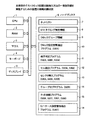
図1は本発明のテストクロック回路自動挿入方法の一実施形態を実施するための装置の概略的構成図である。この装置は、コンピュータからなり、CPU(central processing unit)1、RAM(random access memory)2、マウス3、キーボード4、ディスプレイ5及びハードディスク6等を備えている。
FIG. 1 is a schematic configuration diagram of an apparatus for carrying out an embodiment of a test clock circuit automatic insertion method of the present invention. This apparatus is composed of a computer and includes a central processing unit (CPU) 1, a random access memory (RAM) 2, a
ハードディスク6には、本発明のテストクロック回路自動挿入方法の一実施形態の実施に必要なデータ及びプログラム(本発明のテストクロック回路自動挿入プログラムの一実施形態)が格納され、論理合成後のLSIへのテストクロック回路及び0/1制御回路の自動挿入時には、これらデータ及びプログラムは、ハードディスク6からRAM2に転送される。
The hard disk 6 stores data and a program (one embodiment of the test clock circuit automatic insertion program of the present invention) necessary for carrying out one embodiment of the test clock circuit automatic insertion method of the present invention. These data and programs are transferred from the hard disk 6 to the
本発明のテストクロック回路自動挿入方法の一実施形態の実施に必要なデータとしては、論理合成後テスト容易化設計前のLSIのネットリスト7、STAタイミング制約情報8、及び、システムモード時の周波数の異なる複数のクロックをテストクロック端子数にグループ化するためのクロックグループ情報9がハードディスク6に格納される。
The data necessary for carrying out an embodiment of the test clock circuit automatic insertion method of the present invention includes
また、本発明のテストクロック回路自動挿入方法の一実施形態の実施に必要なプログラムとしては、クロック設定箇所抽出プログラム10、端子判定プログラム11、セル抽出プログラム12、セレクタ挿入プログラム13、グループ化プログラム14、ネット結線プログラム15及び0/1ケース設定箇所抽出プログラム16がハードディスク6に格納される。
The programs necessary for carrying out the test clock circuit automatic insertion method of the present invention include a clock setting
クロック設定箇所抽出プログラム10は、論理合成後テスト容易化設計前のLSIのネットリスト7からSTAでのクロック設定箇所を抽出するプログラムであり、後述するステップS201で使用するものである。
The clock setting
端子判定プログラム11は、クロック設定箇所抽出プログラム10により抽出したSTAでのクロック設定箇所がセル端子であるか否かの判定や、0/1ケース設定箇所抽出プログラム16により抽出した0/1ケース設定箇所がセルの入力端子であるか否かの判定や、セルの出力端子であるか否かの判定を行うプログラムであり、後述するステップS202、S302、S304で使用するものである。
The
セル抽出プログラム12は、クロック設定箇所抽出プログラム10により抽出したSTAでのクロック設定箇所がセルの上位階層のモジュールポートである場合におけるモジュールポートの直前のセルの出力端子の探索や、0/1ケース設定箇所抽出プログラム16により抽出した0/1ケース設定箇所がセルの入力端子でもなく、セルの出力端子でもない場合におけるセルの出力端子の探索を行うプログラムであり、後述するステップS204、S306に使用するものである。
The
セレクタ挿入プログラム13は、クロック設定箇所抽出プログラム10により抽出したクロック設定箇所であるセル端子へのセレクタの挿入や、セル抽出プログラム12により探索したセルの出力端子へのセレクタの挿入や、0/1ケース設定箇所抽出プログラム16により抽出した0/1ケース設定箇所がセルの入力端子である場合におけるセルの入力側へのセレクタの挿入や、0/1ケース設定箇所がセルの出力端子である場合におけるセルの出力側へのセレクタの挿入や、0/1ケース設定箇所がセルの入力端子でもなく、セルの出力端子でもない場合において、セル抽出プログラム12により抽出したセルの出力側へのセレクタの挿入を行うプログラムであり、後述するステップS203、S303、S305に使用するものである。
The
グループ化プログラム14は、セレクタ挿入プログラム13により挿入したセレクタを同一周波数のテストクロックを供給するセレクタごとにグループ化するプログラムであり、後述するステップS205で使用するものである。
The
ネット結線プログラム15は、セレクタ挿入プログラム13により挿入したテストクロック回路を構成するセレクタへのテストクロック端子及びテストモード制御信号の接続や、0/1制御回路を構成するセレクタの入力端子のうち、テストモード時に選択される入力端子の論理0または論理1へのクリップや、同セレクタへのテストモード制御信号の接続を行うプログラムであり、後述するステップS206、S207、S307、S308で使用するものである。
The
0/1ケース設定箇所抽出プログラム16は、論理合成後テスト容易化設計前のLSIのネットリスト7から0/1ケース設定箇所を抽出するプログラムであり、後述するステップS301で使用するものである。なお、本発明のテストクロック回路自動挿入プログラムに含まれる0/1制御回路挿入プログラムは、端子判定プログラム11、セル抽出プログラム12、セレクタ挿入プログラム13、ネット結線プログラム15及び0/1ケース設定個所抽出プログラムを含むものである。
The 0/1 case setting
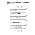
図2は本発明のテストクロック回路自動挿入方法の一実施形態を示すフローチャートである。すなわち、本発明のテストクロック回路自動挿入方法の一実施形態を実施する場合には、まず、論理合成後テスト容易化設計前のLSIのネットリスト7、STAタイミング制約情報8及びクロックグループ情報9をハードディスク6からRAM2に入力する(ステップS1)。
FIG. 2 is a flowchart showing an embodiment of the test clock circuit automatic insertion method of the present invention. That is, when one embodiment of the test clock circuit automatic insertion method of the present invention is implemented, first, the
次に、論理合成後のLSIのSTAでのクロック設定箇所にテストクロック供給可能なテストクロック回路を挿入し(ステップS2)、システムモード時に論理0または論理1に設定される0/1ケース設定箇所の論理値を外部から制御することができる0/1制御回路を挿入し(ステップS3)、テスト容易化設計回路合成を行う(ステップS4)。
Next, a test clock circuit capable of supplying a test clock is inserted into the clock setting location of the LSI STA after logic synthesis (step S2), and the 0/1 case setting location set to
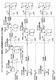
図3はステップS2でのテストクロック回路挿入処理結果例を具体的に示す回路図であり、実線で示す回路部分は、論理合成後テスト容易化設計前のネットリスト7が示すLSIの回路状態の一部分を示し、破線で示す回路部分は、本発明のテストクロック回路自動挿入方法の一実施形態で挿入したテストクロック回路を示している。図3中、20はPLL、21、22は入力セル、23〜25はテストクロック端子、26〜28はフリップフロップからなる2分周器、29はゲーティングクロックセルからなる2分周器、30〜39はテスト時にシフトレジスタを構成するフリップフロップである。
FIG. 3 is a circuit diagram specifically showing an example of the result of the test clock circuit insertion process in step S2. The circuit portion indicated by the solid line indicates the circuit state of the LSI indicated by the
また、40〜46はSTAでのクロック設定箇所であり、40は100MHzのクロックCLK100が設定されるクロック設定箇所、41は50MHzのクロックCLK50が設定されるクロック設定箇所、42は25MHzのクロックCLK25が設定されるクロック設定箇所、43は80MHzのクロックCLK80が設定されるクロック設定箇所、44は40MHzのクロックCLK40が設定されるクロック設定箇所、45は60MHzのクロックCLK60が設定されるクロック設定箇所、46は30MHzのクロックCLK30が設定されるクロック設定箇所、47〜53はテストクロック回路を構成するセレクタである。
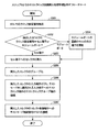
図4はステップS2でのテストクロック回路挿入処理手順を示すフローチャートである。すなわち、論理合成後テスト容易化設計前のLSIにテストクロック回路を挿入する場合には、まず、クロック設定箇所抽出プログラム10により、論理合成後テスト容易化設計前のLSIのネットリスト7からSTAでのクロック設定箇所を抽出する(ステップS201)。図3の例では、STAでのクロック設定箇所40〜46が抽出されることになる。
FIG. 4 is a flowchart showing a test clock circuit insertion processing procedure in step S2. That is, when a test clock circuit is inserted into an LSI after logic synthesis and before design for testability, the clock setting
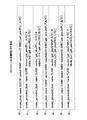
なお、STAクロックは、例えば、図5に示すように定義され、STAタイミング制約情報8中に含まれる。この例では、記述60は、「クロックCLK100は、1周期を10000ピコ秒とし、t=0で立ち上がり、t=5000ピコ秒で立ち下がり、PLL20(PLL_A)の出力端子(X)に設定されるもの」であることを示している。
For example, the STA clock is defined as shown in FIG. 5 and included in the STA
記述61は、「クロックCLK50は、PLL20(PLL_A)の出力端子(X)をソースとし、2分周器26(REG_A)の出力端子(Q)に設定されるもの」であることを示している。記述62は、「クロックCLK25は、PLL20(PLL_A)の出力端子(X)をソースとし、4分周したものであり、2分周器27(REG_B)の出力端子(Q)に設定されるもの」であることを示している。
The
記述63は、「クロックCLK80は、1周期を12500ピコ秒とし、t=0で立ち上がり、t=6259ピコ秒で立ち下がり、入力セル21(INPUT_A)の出力端子(X)に設定されるもの」であることを示している。記述64は、「クロックCLK40は、入力セル21(INPUT_A)の出力端子(X)をソースとし、2分周器28(REG_C)の出力端子(Q)に設定されるもの」であることを示している。
記述65は、「クロックCLK60は、1周期を16600ピコ秒とし、t=0で立ち上がり、t=8300ピコ秒で立ち下がり、入力セル22(INPUT_B)の出力端子(X)に設定されるもの」であることを示している。記述66は、「クロックCLK30は、入力セル22(INPUT_B)の出力端子(X)をソースとし、2分周器29(GCB_A)の出力端子(GCLK)に設定されるもの」であることを示している。
前述のステップS201の後、抽出したSTAでのクロック設定箇所がセル端子であるかモジュールポートであるかを端子判定プログラム11により判定する(ステップS202)。判定の結果、抽出したSTAでのクロック設定箇所がセル端子である場合には、抽出したSTAでのクロック設定箇所であるセル端子にセレクタ挿入プログラム13によりセレクタを挿入する(ステップS203)。
After the aforementioned step S201, the
図3の例では、STAでのクロック設定箇所40〜46は、全てセル端子であるから、クロック設定箇所40〜46にセレクタ47〜53が挿入される。なお、セレクタ47〜53は、テストモード制御信号XTST=“0”の場合には、システムモード時のクロックを選択し、テストモード制御信号XTST=“1”の場合には、テストクロックを選択するものとして挿入される。
In the example of FIG. 3, since the
また、前述のステップS202での判定の結果、抽出したSTAでのクロック設定箇所がモジュールポートである場合には、STAでのクロック設定箇所として抽出したモジュールポートの直前のセルの出力端子をセル抽出プログラム12により探索し(ステップS204)、探索したセルの出力端子にセレクタ挿入プログラム13によりセレクタを挿入する(ステップS203)。
If the result of determination in step S202 is that the clock setting location in the extracted STA is a module port, the cell output is extracted from the output terminal of the cell immediately before the module port extracted as the clock setting location in the STA. A search is performed by the program 12 (step S204), and a selector is inserted by the
次に、クロックグループ情報9及びグループ化プログラム14により、ステップS203で挿入したセレクタを同一のテストクロックを与えるセレクタ毎のグループにグループ化する(ステップS205)。
Next, according to the
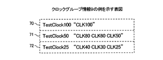
図6はクロックグループ情報9の例を示す表図である。この例の場合には、記述70は、「クロックCLK100は、テストクロックTestClock100のグループにグループ化される」ことを示し、記述71は、「クロックCLK80、CLK60、CLK50は、テストクロックTestClock50のグループにグループ化される」ことを示し、記述72は、「クロックCLK40、CLK30、CLK25は、テストクロックTestClock25のグループにグループ化される」ことを示している。
FIG. 6 is a table showing an example of the
したがって、図3の例の場合には、セレクタ47は、テストクロックTestClock100のグループにグループ化され、セレクタ48〜50は、テストクロックTestClock50のグループにグループ化され、セレクタ51〜53は、テストクロックTestClock25のグループにグループ化されることになる。
Therefore, in the example of FIG. 3, the
次に、挿入されたセレクタの入力端子のうち、テストモード時に選択される入力端子にネット結線プログラム15によりテストクロック端子をグループごとに接続し(ステップS206)、更に、挿入されたセレクタのセレクト制御端子にネット結線プログラム15によりテストモード制御信号XTSTを接続する(ステップS207)。 Next, among the input terminals of the inserted selector, the test clock terminals are connected to the input terminals selected in the test mode for each group by the net connection program 15 (step S206), and the select control of the inserted selector is performed. The test mode control signal XTST is connected to the terminal by the net connection program 15 (step S207).
図3の例では、セレクタ47の入力端子のうち、テストモード制御信号XTST=“1”の場合に選択される入力端子にテストクロック端子23が接続され、セレクタ48〜50の入力端子のうち、テストモード制御信号XTST=“1”の場合に選択される入力端子にテストクロック端子24が接続され、セレクタ51〜53の入力端子のうち、テストモード制御信号XTST=“1”の場合に選択される入力端子にテストクロック端子25が接続され、更に、セレクタ47〜53のセレクト制御端子にはテストモード制御信号XTSTが接続される。
In the example of FIG. 3, the
この結果、テストモード時には、システムモード時に100MHzのクロックCLK100が与えられるフリップフロップ(フリップフロップ30等)には、テストクロックTestClock100として、100MHzのスキャンクロックが供給される。 As a result, in the test mode, a 100 MHz scan clock is supplied as a test clock TestClock 100 to a flip-flop (such as the flip-flop 30) to which a 100 MHz clock CLK100 is applied in the system mode.
また、システムモード時に80MHzのクロックCLK80が与えられるフリップフロップ(フリップフロップ34等)、システムモード時に60MHzのクロックCLK60が与えられるフリップフロップ(フリップフロップ37等)、及び、システムモード時に50MHzのクロックCLK50が与えられるフリップフロップ(フリップフロップ31等)には、テストクロックTestClock50として、50MHzのスキャンクロックが供給される。
Also, a flip-flop (such as flip-flop 34) to which an 80 MHz clock CLK80 is applied in the system mode, a flip-flop (such as flip-flop 37) to which a 60 MHz clock CLK60 is applied in the system mode, and a 50 MHz clock CLK50 in the system mode. A 50 MHz scan clock is supplied as a
また、システムモード時に40MHzのクロックCLK40が与えられるフリップフロップ(フリップフロップ35、36等)、システムモード時に30MHzのクロックCLK30が与えられるフリップフロップ(フリップフロップ38、39等)、及び、システムモード時に25MHzのクロックCLK25が与えられるフリップフロップ(フリップフロップ32、33等)には、テストクロックTestClock25として、25MHzのスキャンクロックが供給される。
Also, flip-flops (flip-
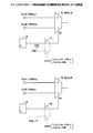
図7はステップS3での0/1制御回路挿入処理結果例を具体的に示す回路図であり、実線で示す回路部分は、論理合成後テスト容易化設計前のLSIのネットリスト7が示す回路状態の一部分を示し、破線で示す部分は、本発明のテストクロック回路自動挿入方法の一実施形態で挿入された0/1制御回路を示している。
FIG. 7 is a circuit diagram specifically showing an example of the result of the 0/1 control circuit insertion process in step S3. The circuit portion shown by the solid line is the circuit shown by the
図7中、75は50MHzのクロックCLKAまたは100MHzのクロックCLKBを選択するセレクタであり、セレクト制御端子S0のレベル=“0”の場合にはクロックCLKAを選択し、セレクト制御端子S0のレベル=“1”の場合にはクロックCLKBを選択するものである。76はセレクタ75のセレクト制御端子S0にセレクト制御信号を与えるフリップフロップ、77は0/1制御回路を構成するセレクタである。
In FIG. 7,
また、78は100MHzのクロックCLKCまたは50MHzのクロックCLKDを選択するセレクタであり、セレクト制御端子S0のレベル=“0”の場合にはクロックCLKCを選択し、セレクト制御端子S0のレベル=“1”の場合にはクロックCLKDを選択するものである。79はセレクタ78のセレクト制御端子S0にセレクト制御信号を与えるフリップフロップ、80は0/1制御回路を構成するセレクタである。
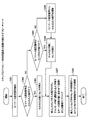
図8はステップS3での0/1制御回路挿入処理手順を示すフローチャートである。すなわち、0/1制御回路を挿入する場合には、まず、0/1ケース設定箇所抽出プログラム16により、論理合成後テスト容易化設計前のLSIのネットリスト7から0/1ケース設定箇所を抽出する(ステップS301)。図7の例では、0/1ケース設定箇所としてセレクタ75、78のセレクト制御端子S0が抽出される。
FIG. 8 is a flowchart showing the 0/1 control circuit insertion processing procedure in step S3. That is, when the 0/1 control circuit is inserted, first, the 0/1 case setting
次に、抽出した0/1ケース設定箇所がセルの入力端子か否かを端子判定プログラム11により判定する(ステップS302)。判定の結果、抽出した0/1ケース設定箇所がセルの入力端子の場合(ステップS302でYESの場合)には、セレクタ挿入プログラム13により、セルの入力側にセレクタを挿入する(ステップS303)。
Next, it is determined by the
図7の例では、セレクタ75のセレクト制御端子S0側にセレクタ77が挿入され、セレクタ78のセレクト制御端子S0側にセレクタ80が挿入される。セレクタ77は、テストモード制御信号XTST=“0”の場合にはフリップフロップ76の出力を選択し、セレクタ80は、テストモード制御信号XTST=“0”の場合にはフリップフロップ79の出力を選択するように挿入される。
In the example of FIG. 7, a
これに対して、抽出した0/1ケース設定箇所がセルの入力端子でない場合(ステップS302でNOの場合)には、抽出した0/1ケース設定箇所がセルの出力端子であるか否かを端子判定プログラム11により判定する(ステップS304)。判定の結果、抽出した0/1ケース設定箇所がセルの出力端子の場合(ステップS304でYESの場合)には、セルの出力側にセレクタを挿入する(ステップS305)。 On the other hand, if the extracted 0/1 case setting location is not the cell input terminal (NO in step S302), it is determined whether or not the extracted 0/1 case setting location is the cell output terminal. This is determined by the terminal determination program 11 (step S304). As a result of the determination, if the extracted 0/1 case setting location is the cell output terminal (YES in step S304), a selector is inserted on the cell output side (step S305).
また、ステップS304での判定の結果、抽出した0/1ケース設定箇所がセルの出力端子でない場合(ステップS304でNOの場合)には、セル抽出プログラム12により、抽出した0/1ケース設定箇所からセルの出力端子を探索し(ステップS306)、探索したセルの出力側にセレクタ挿入プログラム13によりセレクタを挿入する(ステップS305)。
If the extracted 0/1 case setting location is not an output terminal of the cell as a result of the determination in step S304 (NO in step S304), the
次に、挿入したセレクタの入力端子のうち、テストモード時に選択される入力端子をケース設定の値にあわせて論理0または論理1にネット結線プログラム15によりクリップし(ステップS307)、更に、挿入したセレクタのセレクト制御端子にテストモード制御信号をネット結線プログラム15により接続する(ステップS308)。
Next, among the input terminals of the inserted selector, the input terminal selected in the test mode is clipped to the
図7の例では、セレクタ77は、テストモード制御信号XTST=“1”の場合に選択される入力端子が論理1にクリップされ、セレクト制御端子にテストモード制御信号XTSTが接続される。セレクタ80は、テストモード制御信号XTST=“1”の場合に選択される入力端子が論理0にクリップされ、セレクト制御端子にテストモード制御信号XTSTが接続される。
In the example of FIG. 7, in the
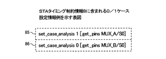
図9はSTAタイミング制約情報8に含まれる0/1ケース設定情報例を示す表図であり、記述85は、「セレクタ75(MUX_A)のセレクト制御端子(S0)には論理1が設定される」ことを示している。記述86は、「セレクタ78(MUX_B)のセレクト制御端子(S0)には論理0が設定される」ことを示している。
FIG. 9 is a table showing an example of 0/1 case setting information included in the STA
以上のように、本発明のテストクロック回路自動挿入方法の一実施形態では、クロック設定箇所抽出プログラム10によるSTAでのクロック設定箇所の抽出(ステップS201)と、端子判定プログラム11、セル抽出プログラム12及びセレクタ挿入プログラム13によるクロック設定箇所にテストクロック供給可能なテストクロック回路を構成するセレクタの挿入(ステップS202〜S204)と、グループ化プログラム14によるテストクロック回路を構成するセレクタのグループ化(ステップS205)と、ネット結線プログラム15によるテストクロック回路を構成するセレクタへのテストクロック端子及びテストモード制御信号XTSTの接続(ステップS206、S207)が実行される。
As described above, in one embodiment of the test clock circuit automatic insertion method of the present invention, the clock setting
さらに、0/1ケース設定箇所抽出プログラム16による0/1ケース設定箇所の抽出(ステップS301)と、端子判定プログラム11、セル抽出プログラム12及びセレクタ挿入プログラム13によるセルの入力側または出力側への0/1制御回路を構成するセレクタの挿入(ステップS302〜S306)と、ネット結線プログラム15による0/1制御回路を構成するセレクタの所定の入力端子の論理0または論理1へのクリップと、0/1制御回路を構成するセレクタのセレクト制御端子へのテストモード制御信号XTSTの接続(ステップS307、S308)が実行される。
Further, the 0/1 case setting
すなわち、本発明のテストクロック回路自動挿入方法の一実施形態によれば、本発明のテストクロック回路自動挿入プログラムの一実施形態を使用し、コンピュータにより、論理合成後のLSIのSTAでのクロック設定箇所を抽出し、該クロック設定箇所にテストクロック供給可能なテストクロック回路を挿入するテストクロック回路挿入工程が実行されるので、論理合成後のLSIに遅延故障の検出が可能なテストクロック回路及び0/1制御回路を自動挿入することができる。したがって、テスト容易化設計工数の低減化を図ることができる。 That is, according to one embodiment of the test clock circuit automatic insertion method of the present invention, the clock setting in the STA of the LSI after logic synthesis is performed by the computer using one embodiment of the test clock circuit automatic insertion program of the present invention. A test clock circuit insertion step is performed for extracting a location and inserting a test clock circuit capable of supplying a test clock to the location where the clock is set. Therefore, a test clock circuit capable of detecting a delay fault in the LSI after logic synthesis and 0 / 1 Control circuit can be automatically inserted. Therefore, it is possible to reduce the man-hours for design for testability.
ここで、本発明を整理すると、本発明には、少なくとも、以下のテストクロック回路自動挿入方法及びプログラムが含まれる。 Here, to summarize the present invention, the present invention includes at least the following test clock circuit automatic insertion method and program.
(付記1)コンピュータにより、論理合成後のLSIのSTAでのクロック設定箇所を抽出し、該クロック設定箇所にテストクロック供給可能なテストクロック回路を挿入するテストクロック回路挿入工程を含むことを特徴とするテストクロック回路自動挿入方法。 (Additional remark 1) It is characterized by including the test clock circuit insertion process which extracts the clock setting location in STA of LSI after logic synthesis by computer, and inserts the test clock circuit which can supply a test clock to this clock setting location Automatic test clock circuit insertion method.
(付記2)前記テストクロック回路挿入工程は、クロック設定箇所抽出プログラムにより、前記LSIから前記クロック設定箇所を抽出するクロック設定箇所抽出工程と、セレクタ挿入プログラムにより、前記クロック設定箇所にテストクロック供給可能なセレクタを挿入するセレクタ挿入工程と、ネット結線プログラムにより、前記セレクタの所定の入力端子にテストクロック端子を接続し、前記セレクタのセレクト制御端子にテストモード制御信号を接続するネット結線工程を含むことを特徴とする付記1記載のテストクロック回路自動挿入方法。
(Supplementary Note 2) The test clock circuit insertion step can supply a test clock to the clock setting location by a clock setting location extraction step for extracting the clock setting location from the LSI by a clock setting location extraction program and a selector insertion program. A selector insertion step of inserting a correct selector, and a net connection step of connecting a test clock terminal to a predetermined input terminal of the selector and connecting a test mode control signal to the select control terminal of the selector by a net connection program. The test clock circuit automatic insertion method according to
(付記3)前記セレクタ挿入工程は、前記クロック設定箇所がセル端子の場合には、該セル端子に前記セレクタを挿入し、前記クロック設定箇所がモジュールポートの場合には、該モジュールポートの直前のセルの出力端子にセレクタを挿入する工程であることを特徴とする付記2記載のテストクロック回路自動挿入方法。
(Supplementary Note 3) In the selector insertion step, when the clock setting location is a cell terminal, the selector is inserted into the cell terminal, and when the clock setting location is a module port, The test clock circuit automatic insertion method according to
(付記4)前記コンピュータにより、システムモード時に論理0または論理1に設定される0/1ケース設定箇所を抽出し、該0/1ケース設定箇所の論理値を外部から制御することができる0/1制御回路を挿入する0/1制御回路挿入工程を含むことを特徴とする付記1、2または3記載のテストクロック回路自動挿入方法。
(Supplementary Note 4) The computer can extract the 0/1 case setting location set to
(付記5)前記0/1制御回路挿入工程は、0/1ケース設定箇所抽出プログラムにより、前記0/1ケース設定箇所を抽出する0/1ケース設定箇所抽出工程と、前記セレクタ挿入プログラムにより、前記0/1ケース設定箇所がセルの入力端子の場合には、該セルの入力側にセレクタを挿入し、前記0/1ケース設定箇所がセルの出力端子の場合には、該セルの出力側にセレクタを挿入し、前記0/1ケース設定箇所がセルの入力端子でもなく、セルの出力端子でもない場合には、セルの出力端子を探索し、該探索したセルの出力側にセレクタを挿入する工程を含むことを特徴とする付記4記載のテストクロック回路自動挿入方法。 (Supplementary Note 5) The 0/1 control circuit insertion step is performed by a 0/1 case setting location extraction program that extracts the 0/1 case setting location by a 0/1 case setting location extraction program, and a selector insertion program. When the 0/1 case setting location is the cell input terminal, a selector is inserted on the cell input side, and when the 0/1 case setting location is the cell output terminal, the cell output side If the 0/1 case setting location is neither the cell input terminal nor the cell output terminal, the cell output terminal is searched and the selector is inserted on the output side of the searched cell. The method for automatically inserting a test clock circuit according to appendix 4, characterized by comprising the step of:
(付記6)論理合成後のLSIのSTAでのクロック設定箇所を抽出し、該クロック設定箇所にテストクロック供給可能なテストクロック回路を挿入するテストクロック回路挿入工程をコンピュータに実行させることを特徴とするテストクロック回路自動挿入プログラム。 (Additional remark 6) It is characterized by having a computer execute a test clock circuit insertion step of extracting a clock setting location in an STA of an LSI after logic synthesis and inserting a test clock circuit capable of supplying a test clock to the clock setting location. Test clock circuit automatic insertion program.
(付記7)前記クロック設定箇所を抽出するクロック設定箇所抽出工程を前記コンピュータに実行させるクロック設定箇所抽出プログラムと、前記クロック設定箇所にテストクロック供給可能なセレクタを挿入するセレクタ挿入工程を前記コンピュータに実行させるセレクタ挿入プログラムと、前記セレクタの所定の入力端子にテストクロック端子を接続し、前記セレクタのセレクト制御端子にテストモード制御信号を接続するネット結線工程を前記コンピュータに実行させるネット結線プログラムを含むことを特徴とする付記6記載のテストクロック回路自動挿入プログラム。 (Supplementary note 7) A clock setting location extraction program for causing the computer to execute a clock setting location extraction process for extracting the clock setting location, and a selector insertion step for inserting a selector capable of supplying a test clock to the clock setting location in the computer A selector insertion program to be executed, and a net connection program for causing the computer to execute a net connection step of connecting a test clock terminal to a predetermined input terminal of the selector and connecting a test mode control signal to a select control terminal of the selector The test clock circuit automatic insertion program according to appendix 6, characterized in that:
(付記8)前記クロック設定箇所がセル端子であるか否かの判定を行う端子判定工程を前記コンピュータに実行させる端子判定プログラムを含み、前記セレクタ挿入プログラムは、前記クロック設定箇所がセル端子の場合には、該セル端子に前記セレクタを挿入し、前記クロック設定箇所がモジュールポートの場合には、該モジュールポートの直前のセルの出力端子にセレクタを挿入するものであることを特徴とする付記7記載のテストクロック回路自動挿入プログラム。 (Supplementary Note 8) A terminal determination program for causing the computer to execute a terminal determination step for determining whether or not the clock setting location is a cell terminal, wherein the selector insertion program includes the case where the clock setting location is a cell terminal In the above, the selector is inserted into the cell terminal, and when the clock setting location is a module port, the selector is inserted into the output terminal of the cell immediately before the module port. The test clock circuit automatic insertion program described.
(付記9)システムモード時に論理0または論理1に設定される0/1ケース設定箇所を抽出し、該0/1ケース設定箇所の論理値を外部から制御することができる0/1制御回路を挿入する0/1制御回路挿入工程を前記コンピュータに実行させる0/1制御回路挿入プログラムを含むことを特徴とする付記6、7または8記載のテストクロック回路自動挿入プログラム。
(Supplementary Note 9) A 0/1 control circuit capable of extracting a 0/1 case setting location set to
(付記10)前記0/1制御回路挿入プログラムには、前記0/1ケース設定箇所を抽出する0/1ケース設定箇所抽出工程を前記コンピュータに実行させる0/1ケース設定箇所抽出プログラムと、前記0/1ケース設定箇所がセルの入力端子の場合には、該セルの入力側にセレクタを挿入し、前記0/1ケース設定箇所がセルの出力端子の場合には、該セルの出力側にセレクタを挿入し、前記0/1ケース設定箇所がセルの入力端子でもなく、セルの出力端子でもない場合には、セルの出力端子を探索し、該探索したセルの出力側にセレクタを挿入する工程を前記コンピュータに実行させるセレクタ挿入プログラムを含むことを特徴とする付記9記載のテストクロック回路自動挿入プログラム。
(Supplementary Note 10) The 0/1 control circuit insertion program includes a 0/1 case setting location extraction program for causing the computer to execute a 0/1 case setting location extraction process for extracting the 0/1 case setting location, When the 0/1 case setting location is the cell input terminal, a selector is inserted on the cell input side, and when the 0/1 case setting location is the cell output terminal, the selector is inserted on the cell output side. If a selector is inserted and the 0/1 case setting location is neither a cell input terminal nor a cell output terminal, the cell output terminal is searched and the selector is inserted on the output side of the searched cell. The program for automatically inserting a test clock circuit according to
1…CPU
2…RAM
3…マウス
4…キーボード
5…ディスプレイ
6…ハードディスク
7…ネットリスト
8…STAタイミング制約情報
9…クロックグループ情報
10…クロック設定箇所抽出プログラム
11…端子判定プログラム
12…セル抽出プログラム
13…セレクタ挿入プログラム
14…グループ化プログラム
15…ネット結線プログラム
16…0/1ケース設定箇所抽出プログラム
20…PLL
21、22…入力セル
23〜25…テストクロック端子
26〜29…2分周器
30〜39…フリップフロップ
40〜46…STAでのクロック設定箇所
47〜53…セレクタ
75…セレクタ
76…フリップフロップ
77、78…セレクタ
79…フリップフロップ
80…セレクタ
1 ... CPU
2 ... RAM
DESCRIPTION OF
21, 22 ...
Claims (5)
前記クロック設定箇所にテストクロック供給可能なセレクタを挿入するセレクタ挿入工程を前記コンピュータに実行させるセレクタ挿入プログラムと、
前記セレクタの所定の入力端子にテストクロック端子を接続し、前記セレクタのセレクト制御端子にテストモード制御信号を接続するネット結線工程を前記コンピュータに実行させるネット結線プログラムを含むことを特徴とする請求項2記載のテストクロック回路自動挿入プログラム。 A clock setting location extraction program for causing the computer to execute a clock setting location extraction process for extracting the clock setting location;
A selector insertion program for causing the computer to execute a selector insertion step of inserting a selector capable of supplying a test clock at the clock setting location;
A network connection program for causing the computer to execute a network connection process for connecting a test clock terminal to a predetermined input terminal of the selector and connecting a test mode control signal to a select control terminal of the selector. 2. A test clock circuit automatic insertion program according to 2.
前記セレクタ挿入プログラムは、前記クロック設定箇所がセル端子の場合には、該セル端子に前記セレクタを挿入し、前記クロック設定箇所がモジュールポートの場合には、該モジュールポートの直前のセルの出力端子にセレクタを挿入するものであることを特徴とする請求項3記載のテストクロック回路自動挿入プログラム。 A terminal determination program for causing the computer to execute a terminal determination step of determining whether or not the clock setting location is a cell terminal;
The selector insertion program inserts the selector into the cell terminal when the clock setting location is a cell terminal, and outputs the output terminal of the cell immediately before the module port when the clock setting location is a module port. 4. The test clock circuit automatic insertion program according to claim 3, wherein a selector is inserted into the test clock circuit.
A 0/1 control circuit that can extract a 0/1 case setting location that is set to logic 0 or 1 in the system mode and can control the logic value of the 0/1 case setting location from the outside is inserted. 5. The test clock circuit automatic insertion program according to claim 2, further comprising a 0/1 control circuit insertion program for causing the computer to execute a 1 control circuit insertion step.
Priority Applications (1)
| Application Number | Priority Date | Filing Date | Title |
|---|---|---|---|
| JP2006180996A JP2008009823A (en) | 2006-06-30 | 2006-06-30 | Test clock circuit automatic insertion method and program |
Applications Claiming Priority (1)
| Application Number | Priority Date | Filing Date | Title |
|---|---|---|---|
| JP2006180996A JP2008009823A (en) | 2006-06-30 | 2006-06-30 | Test clock circuit automatic insertion method and program |
Publications (1)
| Publication Number | Publication Date |
|---|---|
| JP2008009823A true JP2008009823A (en) | 2008-01-17 |
Family
ID=39067953
Family Applications (1)
| Application Number | Title | Priority Date | Filing Date |
|---|---|---|---|
| JP2006180996A Withdrawn JP2008009823A (en) | 2006-06-30 | 2006-06-30 | Test clock circuit automatic insertion method and program |
Country Status (1)
| Country | Link |
|---|---|
| JP (1) | JP2008009823A (en) |
-
2006
- 2006-06-30 JP JP2006180996A patent/JP2008009823A/en not_active Withdrawn
Similar Documents
| Publication | Publication Date | Title |
|---|---|---|
| US8819507B2 (en) | Field programmable gate arrays with built-in self test mechanisms | |
| US11216607B2 (en) | Double glitch capture mode power integrity analysis | |
| US12572727B2 (en) | Static timing analysis method and static timing analysis system | |
| US9449127B1 (en) | System for verifying timing constraints of IC design | |
| US20150227410A1 (en) | Hardware state data logger for silicon debug | |
| CN117907812B (en) | Circuit detection method and device, electronic device, storage medium, and program product | |
| US8042074B2 (en) | Circuit design device, circuit design program, and circuit design method | |
| US8799731B2 (en) | Clock control for reducing timing exceptions in scan testing of an integrated circuit | |
| US10963613B1 (en) | Partial reconfiguration of integrated circuits using shell representation of platform design with extended routing region | |
| CN114880975B (en) | A method, system, device, and medium for generating a hardware Trojan. | |
| US9280623B2 (en) | Signal selection apparatus and system, and circuit emulator and method and program | |
| US7945882B2 (en) | Asynchronous circuit logical verification method, logical verification apparatus, and computer readable storage medium | |
| US20090288046A1 (en) | Circuit design processes | |
| US20170356959A1 (en) | Implementing decreased scan data interdependence for compressed patterns in on product multiple input signature register (opmisr) through scan skewing | |
| US20050223345A1 (en) | Circuit design assistant system, circuit design method, and program product for circuit design | |
| US7962875B2 (en) | Method, apparatus and program for designing circuits | |
| US20080148209A1 (en) | Method of designing semiconductor integrated circuit using test point insertion adjustable to delay time | |
| Lin et al. | Speed binning with high-quality structural patterns from functional timing analysis (FTA) | |
| US10416232B1 (en) | Timing optimizations in circuit designs using opposite clock edge triggered flip-flops | |
| US7086015B2 (en) | Method of optimizing RTL code for multiplex structures | |
| US8468407B2 (en) | Method for creating test clock domain during integrated circuit design, and associated computer readable medium | |
| JP2002073712A (en) | Circuit generation device, circuit generation method, and CAD design device | |
| Pomeranz et al. | Forward-Looking Reverse Order Fault Simulation for $ n $-Detection Test Sets | |
| JP2012003684A (en) | Circuit design device, circuit design program and circuit design method | |
| JP2007226686A (en) | Critical path estimation program, estimation apparatus, estimation method, and integrated circuit design program. |
Legal Events
| Date | Code | Title | Description |
|---|---|---|---|
| A711 | Notification of change in applicant |
Free format text: JAPANESE INTERMEDIATE CODE: A712 Effective date: 20080730 |
|
| A621 | Written request for application examination |
Free format text: JAPANESE INTERMEDIATE CODE: A621 Effective date: 20090302 |
|
| A761 | Written withdrawal of application |
Free format text: JAPANESE INTERMEDIATE CODE: A761 Effective date: 20101126 |