JP2007534062A - Barcode scanner with linear automatic gain control (AGC), modulation transfer function detector, and selectable noise filter - Google Patents
Barcode scanner with linear automatic gain control (AGC), modulation transfer function detector, and selectable noise filter Download PDFInfo
- Publication number
- JP2007534062A JP2007534062A JP2007508380A JP2007508380A JP2007534062A JP 2007534062 A JP2007534062 A JP 2007534062A JP 2007508380 A JP2007508380 A JP 2007508380A JP 2007508380 A JP2007508380 A JP 2007508380A JP 2007534062 A JP2007534062 A JP 2007534062A
- Authority
- JP
- Japan
- Prior art keywords
- analog signal
- frequency portion
- gain element
- frequency
- amplitude
- Prior art date
- Legal status (The legal status is an assumption and is not a legal conclusion. Google has not performed a legal analysis and makes no representation as to the accuracy of the status listed.)
- Pending
Links
Images


Classifications
-
- G—PHYSICS
- G06—COMPUTING; CALCULATING OR COUNTING
- G06K—GRAPHICAL DATA READING; PRESENTATION OF DATA; RECORD CARRIERS; HANDLING RECORD CARRIERS
- G06K7/00—Methods or arrangements for sensing record carriers, e.g. for reading patterns
- G06K7/10—Methods or arrangements for sensing record carriers, e.g. for reading patterns by electromagnetic radiation, e.g. optical sensing; by corpuscular radiation
- G06K7/10544—Methods or arrangements for sensing record carriers, e.g. for reading patterns by electromagnetic radiation, e.g. optical sensing; by corpuscular radiation by scanning of the records by radiation in the optical part of the electromagnetic spectrum
- G06K7/10821—Methods or arrangements for sensing record carriers, e.g. for reading patterns by electromagnetic radiation, e.g. optical sensing; by corpuscular radiation by scanning of the records by radiation in the optical part of the electromagnetic spectrum further details of bar or optical code scanning devices
- G06K7/10851—Circuits for pulse shaping, amplifying, eliminating noise signals, checking the function of the sensing device
Abstract
本発明の諸実施形態によれば、バーコードを表すアナログ信号の利得が、制御ループを使用して制御されるバーコード・スキャナ・プラットフォームが提供される。諸実施形態では、MTF検出器が、アナログ信号の低周波数部分(幅広い諸要素、つまり光学焦点が合っていない諸要素)を表す値(例えば、DC)、およびアナログ信号の高周波数部分(狭い諸要素、つまり光学焦点が合っている諸要素)を表す第2の値(例えば、DC)を生成する。プロセッサは、第1の値および第2の値、ならびに基準振幅を使用して、利得IE信号を算出する。プロセッサは、利得信号をAGC回路に供給し、回路は、整合JFETを使用して、その利得信号に対する線形応答を供給する。雑音フィルタが、第1の値、第2の値、および/またはバーコード・スキャナ・プラットフォーム読み取り率に基づいて有効にされる、または無効にされることが可能である。 In accordance with embodiments of the present invention, a bar code scanner platform is provided in which the gain of an analog signal representing a bar code is controlled using a control loop. In embodiments, the MTF detector has a value (eg, DC) that represents a low frequency portion of the analog signal (wide elements, ie, elements that are not optically focused), and a high frequency portion of the analog signal (narrow portions). A second value (e.g., DC) representing the element, i.e., elements in optical focus, is generated. The processor calculates the gain IE signal using the first and second values and the reference amplitude. The processor provides a gain signal to the AGC circuit, which uses a matching JFET to provide a linear response to the gain signal. The noise filter can be enabled or disabled based on the first value, the second value, and / or the barcode scanner platform reading rate.
Description
本発明の諸実施形態は、バーコード・スキャナに関し、特に、バーコード・スキャナにおける信号調整に関する。 Embodiments of the invention relate to bar code scanners, and more particularly to signal conditioning in bar code scanners.
バーコードは、消費財を識別することを含む多くの用途を有する。商人は、商品にバーコードを付け、例えば、レジでバーコードを走査して、その特定の商品の価格を明らかにする。図1は、バーコード走査プラットフォーム100の高レベルのブロック図である。プラットフォーム100は、光信号105を発するスキャナ104を使用して走査されるバーコード102を含む。変調された光信号107が、バーコード102から反射され、光検出器−入力段106が、変調された光信号107を、バーコード102を表すアナログ信号108に変換する。信号コンディショナ110が、そのアナログ信号108を処理して、バーコード102を表すデジタル信号112を生成する。
Bar codes have many uses, including identifying consumer goods. The merchant attaches a barcode to the item and scans the barcode at the cash register, for example, to reveal the price of that particular item. FIG. 1 is a high level block diagram of a
例示的なバーコード102は、異なるコントラストと異なる幅の一連のバー120と、スペース122を含む。バー120とスペース122の特定の配置と幅が、コードを形成し、そのコードが復号化されて、プラットフォーム100のユーザに意味のある情報を提供する。
The
図示される実施形態では、バー120はスペース122より暗い。バー120は、スペース122より暗いため、バー120は、スペース122よりも吸収率が高く、反射率が低い。その結果、バー120は、アナログ信号108において負のピークを生じさせ、スペースは、アナログ信号108において正のピークを生じさせる。
In the illustrated embodiment, the bar 120 is darker than the space 122. Since the bar 120 is darker than the space 122, the bar 120 has higher absorptance and lower reflectance than the space 122. As a result, the bar 120 produces a negative peak in the
光信号105は、一般に、バーコードを走査する焦点が合わせられた光学「スポット」であり、スポットのサイズは、バーコード102の読み取りに影響を与える。例えば、光学スポット・サイズが、最小のバー120、または最小のスペース122より小さい場合、光信号105は、光学「焦点」の範囲内にあると言われ、アナログ信号108は、バーコード102のかなり良好な表現である。「焦点が合わせられた」信号の1つの特性は、最も狭いバー120Aと最も狭いスペース122Bに関するアナログ信号108における正のピークと負のピークが、より幅広いバー120Cとより幅広いスペース122Cの場合と同一の振幅であることである。
The
走査レーザ104が、光学焦点から引き離されるにつれ(例えば、バーコード102からより遠く、またはバーコード120により近く)、光学スポット・サイズは、より大きくなる。より大きい光学スポットでは、光信号105のエネルギーが、隣接する複数のバー120と複数のスペース122にわたって分散されて、利用できるエネルギーのすべてを吸収する特定の1つのバー120が無いか、または利用できるエネルギーの全てを反射する特定の1つのスペースが無くなる。その結果、最も狭いバー(例えば、120A、120D)と最も狭いスペース(例えば、122B)に関する負のピークと正のピークが、より幅広いバー120Cや幅広いスペース122Cの場合よりも小さい振幅を有する。
As the
バーコード走査プラットフォームと焦点ポイントの1つの特性は、ときとして、狭いバーと狭いスペースに関連するアナログ信号108の部分の振幅が、より幅広いバーとより幅広いスペースに関連するアナログ信号108の部分の振幅とは異なる(例えば、より小さい)ことである。これは、光学スポット・サイズが、最も狭いバーと最も狭いスペースより大きい場合によくある。狭いバーと狭いスペースに関連するアナログ信号108の部分の振幅と、幅広いバーと幅広いスペースに関連するアナログ信号108の部分の振幅との比は、「変調伝達関数」またはMTFと呼ばれ、アナログ信号108の特性を記述するのに使用される。例えば、MTFが、100パーセント(100%)より小さい場合、アナログ信号108が、バーコード102を表すデジタル信号に正確に分解されるのは困難である可能性がある。
One characteristic of the bar code scanning platform and the focal point is that sometimes the amplitude of the portion of the
バーコード走査プラットフォームの別の特性は、光学スポット・サイズが、非常に小さくなるにつれ(例えば、焦点ポイントで)、光信号105のエネルギーが、バーコード102を担持する材料(例えば、紙繊維、木の削り屑、金属ピット、グレインなど)上により集中することである。繊維、グレイン、ピットなど自体が、光信号105のエネルギーを吸収および/または反射することを始め、「ペーパ・ノイズ」と一般に呼ばれるものを生じさせる。ペーパ・ノイズは、アナログ信号108の信号対雑音比(SNR)を低下させる傾向がある。また、その他の雑音も、プラットフォームに導入される可能性がある。アナログ信号108のSNRが低下すると、アナログ信号108が、バーコード102を表すデジタル信号に正確に分解されるのが困難であろう。
Another characteristic of the bar code scanning platform is that as the optical spot size becomes very small (eg, at the focal point), the energy of the
バーコード走査プラットフォームのさらに別の特性は、アナログ信号108が、バーコード102を表すデジタル信号に正確に分解されるために、一定の振幅を保持しなければならないことである。自動利得制御回路が、従来、振幅を一定に保つのに使用されていた。しかし、多くの既知の自動利得制御技術は複雑な制御式や高価格の回路を要求する。
Yet another property of the barcode scanning platform is that the
図面では、同様の符号が、一般に、同一の要素、機能的に類似した要素、および/または構造的に均等の要素を示す。要素が最初に出現する図面は、符号の左端の数字によって示される。 In the drawings, like reference numbers generally indicate identical, functionally similar, and / or structurally equivalent elements. The drawing in which an element first appears is indicated by the leftmost digit (s) in the reference number.
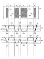
図2は、本発明の実施形態による、バーコード102を表すアナログ信号202、203とそのアナログ信号202、203に関する基準振幅204(例えば、ピーク、ピーク幅)に関連して、バーコード102に対する信号202、203の関係を表すグラフである。図示される実施形態では、アナログ信号202は、負のピーク群220(例えば、220A、220B、220C、220D)と正のピーク群222(例えば、222A、222B、222C)とを含む、変調された信号である。負のピーク群220は、バー120を表し、正のピーク群222は、スペース122を表す。アナログ信号203は、負のピーク群230(例えば、230A、230B、230C、230D)と正のピーク群232(例えば、232A、232B、232C)とを含む、変調された信号である。負のピーク群230は、バー120を表し、正のピーク群232は、スペース122を表す。図示される実施形態では、アナログ信号203は、およそ100パーセント(100%)の変調伝達関数を有し、アナログ信号202は、100パーセント(100%)より低い変調伝達関数を有する。
FIG. 2 illustrates a signal for a
バー120Aは、バー120D(例えば、1×要素幅)と同一の幅であり、バー120B(例えば、2×要素幅)より狭い。バー120D、120Bは、バー120C(3×要素幅)より狭い。スペース122B(例えば、1×要素幅)は、スペース122A(例えば、3×要素幅)とスペース122C(例えば、やはり3×要素幅)より狭い。
The
例示的なアナログ信号203では、ピーク群230とピーク群232のすべてが、基準振幅204とほぼ等しい振幅を有する。ピーク群230とピーク232群のすべては、ほぼ同一の振幅を有する(例えば、変調伝達関数が、100パーセント(100%)にほぼ等しいために)。ピーク群230とピーク群232の一部のピークは、異なる要素サイズ(例えば、1×、2×、3×)からもたらされる、互いに異なる周期(例えば、基本周波数)を有する。
In the exemplary
図示される実施形態では、アナログ信号203において、ピーク230A、230D、232Bの周期は、ピーク230B、230C、232A、232Cの周期より短い。ピーク230A、230B、230D、232Bの周期はすべて、ピーク230C、232A、232Cの周期より短い。例示的なアナログ信号203は、100パーセント(100%)にほぼ等しい変調伝達関数を有し、したがって、バーコード102要素120、122のサイズの違いに関わらず、さらに、そのため、関連するピークの周期の違いに関わらず、正のピーク群232と負のピーク群230は、ほぼ等しい振幅を有する。
In the illustrated embodiment, in the
例示的なアナログ信号202では、ピーク群220とピーク群222の一部のピークは、基準振幅204とは異なる振幅を有する。ピーク群220とピーク群222の一部のピークは、互いに異なる振幅を有する(例えば、変調伝達関数が、光学スポット焦点および/または電子帯域幅に起因して、100パーセント未満(<100%)であるために)。ピーク群220とピーク群222の一部のピークは、異なる要素サイズ(例えば、1×、2×、3×)からもたらされる、互いに異なる周期(例えば、基準周波数)を有する。
In the exemplary
例示的なアナログ信号202では、ピーク220A、220D、222Bの周期は、ピーク220Bの周期より短い。ピーク220A、220B、220D、222Bの周期は、ピーク220C、222A、222Cの周期より短い。
In the exemplary
図3は、本発明の実施形態による信号コンディショナ300の高レベルのブロック図であり、コンディショナ300は、ピーク群230とピーク群232、およびピーク群220とピーク群222の一部のピーク、またはすべてのピークを増幅する、または減衰させる制御ループである。また、信号コンディショナ300は、アナログ信号202/203から雑音を選択的に濾波して除くこともできる。
FIG. 3 is a high level block diagram of a
図示される実施形態における信号コンディショナ300は、デジタイザ306に出力が結合された自動利得制御回路(AGC)回路304を含む。デジタイザ306の出力は、プロセッサ308に結合される。変調伝達関数(MTF)検出器310が、アナログ信号202/203の一部分をタップするように結合される。選択可能な雑音フィルタ312が、AGC回路304の入力とプロセッサ308に結合される。
The
AGC回路304は、入力に線形応答を与えることができ、したがって、アナログ信号202/203を増幅する、または減衰させる。本発明の諸実施形態によるAGC回路304の実施は、図4および図5に関連して以下により詳細に説明する。
The
デジタイザ306が、アナログ信号202/203を受信し、その信号202/203を、バーコード102を表すデジタル信号314(例えば、方形波)に変換する。一実施形態では、デジタイザ306の性能は、アナログ信号202/203が、基準振幅204の範囲内にある場合に、最適である。デジタイザ306を実施するのに適した回路は、知られている。
A
MTF検出器310が、アナログ信号202/203の少なくとも1つの低周波数部分のピーク振幅と、アナログ信号202/203の少なくとも1つの高周波数部分のピーク振幅を検出する。MTF検出器310は、Gain Low信号を生成し、この信号は、一実施形態では、アナログ信号202/203における低周波数ピークを表す直流(DC)レベルである。また、MTF検出器は、Gain High信号も生成し、この信号は、一実施形態では、アナログ信号202/203における高周波数ピークを表すDCレベルである。もちろん、Gain Low信号とGain High信号は、アナログ信号202/203における低周波数ピークと高周波数ピークをそれぞれ表す任意の適切な信号でよい。本発明の諸実施形態によるMTF検出器310の実施は、図6に関連して以下により詳細に説明する。
選択可能な雑音フィルタ312が、AGC回路304の入力に結合されて、アナログ信号202/203の雑音を減衰させ、かつ/または信号対雑音比(SNR)を向上させることが可能である。本発明の諸実施形態による選択可能な雑音フィルタ312の実施は、図5と図7に関連して以下により詳細に説明する。
A
本発明の諸実施形態では、プロセッサ308は、デジタル信号314を復号化することができ、Gain High信号とGain Low信号を測定して、デジタル値に変換し、デジタル値を測定し、デジタル値を基準振幅204と比較し、アナログ信号202/203が増幅されるべきか、または減衰させられるべきか、またはそのままであるべきかを判定する。本明細書の説明を読んだ後、本発明の諸実施形態によるプロセッサ308をどのように実施するかは、当業者には明白となろう。
In embodiments of the present invention, the
図4は、本発明の実施形態による信号コンディショナ300によって実施されるプロセス400を示す流れ図である。プロセス400のオペレーションは、本発明の諸実施形態を理解するのに最も役立つ形で順に実行される複数の別々のブロックとして説明される。しかし、それらのオペレーションが説明される順序は、それらのオペレーションが、必然的に順序依存であること、またはオペレーションが、ブロックが提示される順序で実施されるべきことを意味するものと解釈されてはならない。
FIG. 4 is a flow diagram illustrating a
もちろん、プロセス400は、単に例示的なプロセスであり、他のプロセスを使用して、本発明の諸実施形態を実施してもよい。マシン可読命令を担持するマシンアクセス可能な媒体を使用して、マシン(例えば、プロセッサ)がプロセス400を実行するようにさせてもよい。
Of course,
ブロック402で、AGC回路304が、光検出器と入力段106からアナログ信号202/203を受け取り、そのアナログ信号202/203に、基準振幅204に基づいて利得または減衰を与える。一実施形態では、プロセッサ308は、基準振幅204を表す利得信号をAGC回路304に供給し、回路304は、その利得信号を、アナログ信号202/203を増幅するため、または減衰させるための基準として使用する。
At
ブロック404で、MTF検出器310が、アナログ信号202/203の一部分をタップし、アナログ信号202/203の少なくとも1つの低周波数部分のピーク振幅を検出し、アナログ信号202/203の少なくとも1つの高周波数部分のピーク振幅を検出する。
At
ブロック406で、プロセッサ308が、基準振幅204、Gain High信号とGain Low信号に関連するアルゴリズムに基づいて新たな利得信号を選択し、その新たな利得信号をAGC回路304に加える。一実施形態では、プロセッサ308は、Gain High信号が、Gain Low信号および基準振幅204と比べて不釣合いに小さいと判定する。その実施形態では、新たな利得信号によって、アナログ信号202/203を増幅することを行うよう、AGC回路304に通知する。その際、そのような増幅により、Gain Low信号が、基準振幅204を超えるようになるかどうかに関わらない。
At
代替の実施形態では、Gain Low信号は、Gain High信号とほぼ等しいが、アナログ信号202/203は、基準振幅204未満である。その実施形態では、新たな利得信号は、アナログ信号202/203を増幅して、その信号202/203を基準振幅204の範囲内にするよう、AGC回路304に知らせる。もちろん、他の振幅スキームや減衰スキームも可能であり、本明細書の説明を読んだ後、Gain High値、Gain Low値、基準振幅204値の様々な組合せのために、本発明の諸実施形態をどのように実施するかは、当業者には直ちに認識されよう。
In an alternative embodiment, the Gain Low signal is approximately equal to the Gain High signal, but the
ブロック408で、AGC回路304が、アナログ信号202/203を増幅する、または減衰させるための基準として新たな利得信号を使用する。
At
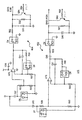
図5は、本発明の実施形態によるAGC回路304の概略図である。図示される実施形態では、AGC回路308は、キャパシタC4(0.1μF)、C10(0.1μF)、C15(39pF)、C17(0.1μF)、C21(12pF)、C22(30μF)、C24(580pF)、C30(100pF)、演算増幅器U3A(非反転)、演算増幅器U4(反転)、トランジスタQ4(補償接合電界効果トランジスタ(JFET))、トランジスタQ7(電圧制御抵抗器の役割をする利得JFET)、抵抗器R4(24Ω)、R8(5.1Ω)、R19(24Ω)、R21(10KΩ)、R24(24Ω)、R26(10KΩ)、R28(4.7KΩ)、R32(20KΩ)、R35(100KΩ)、R39(100KΩ)、R41(100KΩ)、R43(100KΩ)、R46(8.2KΩ)、R47(10KΩ)を含む。
FIG. 5 is a schematic diagram of an
C21は、雑音をロールオフし、増幅器U3Aに信号安定性を与える高周波数補償フィルタを構成する。C22、R24は、U4とFET Q7に関するバイアス電圧が、相互に作用して、アナログ信号202/203に関する不適切なDC出力オフセットと非対称性をもたらすのを低減させる低周波数DCブロッキング・フィルタを構成する。R19とC10およびR4とC4は、U3Aのための電源(例えば、5ボルト)フィルタである。R26とJFET Q7の等価抵抗により、U3Aの利得が決まる。JFET Q4とQ7は、整合トランジスタである。R41、R43、C24は、メイン利得JFET Q7のためのバイアス素子である。R35、R39、C17は、調整JFET Q4のための同様のバイアス素子である。R21、R28は、Q7によって見られる、Q4に対する同様のインピーダンスを提供する。U4は、Q7、Q4のゲートを駆動し、プロセッサ308からのアナログ信号で制御される。R47、R46、C30は、所望される正確なJFETゲート制御のための利得調整を可能にする。
C21 constitutes a high frequency compensation filter that rolls off noise and provides signal stability to amplifier U3A. C22, R24 form a low frequency DC blocking filter that reduces the bias voltage on U4 and FET Q7 interacting to cause inappropriate DC output offset and asymmetry on
プロセッサ308からの利得信号はU4を制御する。U4は、利得信号をバッファリングして、JFET Q7とJFET Q4を駆動する。JFET Q4は、U4の正のフィードバック・パスにある。プロセッサ308からの利得信号に基づき、U4は、JFET Q7にゲート電圧を出力し、JFET Q7は、JFET Q7の特性曲線に従って応答して、等価抵抗をもたらす。U4は、JFET Q4にもゲート電圧を出力し、JFET Q4も、JFET Q4の特性曲線に従って応答して、調整応答をU4に戻す。
The gain signal from
JFET Q4は、JFET Q7と同様のインピーダンスによって駆動され、負荷がかけられており、JFET Q4は、U4の調整フィードバック・パスにあるため、AGC回路304からの出力は、非常に広いダイナミック・レンジにわたって線形であることが可能である(これにより、非常に幅広い範囲の読み取り距離、例えば、バーコード102に近い読み取り距離と、バーコード102から遠く離れた読み取り距離とすることができる)。実施するのに、複雑な制御式を要求し、しばしば、予測利得調整を制限する既知の他の回路とは異なり、本発明の諸実施形態に従って実施されるAGC回路304は、安価な整合JFETを使用して、利得信号入力に対する応答を線形化する。その結果、プロセッサ308からの利得信号に対するAGC回路304の応答は、予測され、決定論的である。
JFET Q4 is driven and loaded with the same impedance as JFET Q7, and because JFET Q4 is in the regulated feedback path of U4, the output from the
AGC回路304が、アナログ信号202/203を減衰させることが可能な代替の実施形態では、AGC回路304は、R8のすぐ後に結合されたJFET Q7を含む。その実施形態では、JFET Q7ドレインが、アースに結合され、U3Aのプラス入力に分圧電圧を供給する、R8とJFET Q7の等価抵抗の間における電圧分圧器を形成する。
In an alternative embodiment where the
本発明のさらに別の実施形態では、AGC回路304は、1つだけのJFET Q7を含み、この実施形態では、回路304の非線形応答(例えば、応答曲線)がプロセッサ308によってマップされる。マップされた値は、格納され(例えば、ルックアップ・テーブルの中に)、プロセッサ308は、マップされた値を使用して、同一の予測利得調整を生成する。
In yet another embodiment of the invention, the
本発明の諸実施形態は、JFETであるQ4とQ7に関連して説明されているが、本発明の諸実施形態は、そのように限定されない。例えば、Q4および/またはQ7は、バイポーラ接合トランジスタ(BJT)、MOSFET、真空管、ガリウム・ヒ素(GaAs)FET、ヘテロ接合バイポーラ接合トランジスタ(HBJT)などを含むが、以上には限定されない、任意の適切な利得素子であることが可能である。本明細書の説明を読んだ後、本発明の他の様々な実施形態におけるQ4とQ7をどのように実施するかは、当業者には明白となろう。 Although embodiments of the present invention have been described in connection with JFETs Q4 and Q7, embodiments of the present invention are not so limited. For example, Q4 and / or Q7 may include any suitable, but not limited to, bipolar junction transistor (BJT), MOSFET, vacuum tube, gallium arsenide (GaAs) FET, heterojunction bipolar junction transistor (HBJT), etc. It is possible to be a simple gain element. After reading the description herein, it will be clear to those skilled in the art how to implement Q4 and Q7 in other various embodiments of the present invention.
図4を再び参照する。ブロック404において、MTF検出器310が、アナログ信号202/203の一部分をタップし、アナログ信号202/203の少なくとも1つの周波数部分(例えば、低周波数)のピーク振幅を検出し、アナログ信号202/203の少なくとも1つの他の周波数部分(例えば、高周波数)のピーク振幅を検出することを思い起こされたい。図6は、本発明の実施形態によるMTF検出器310の概略図である。図示される実施形態では、MTF検出器310は、2つの周波数検出回路602、604を含む。一実施形態では、周波数検出回路602は、およそ2、3百キロヘルツから、およそ5、6百キロヘルツまでのレンジにおけるアナログ信号202/203内の高い方の周波数を検出する。別の実施形態では、周波数検出回路604は、およそ数十キロヘルツから、およそ2、3百キロヘルツまでのレンジにおけるアナログ信号202/203内の低い方の周波数を検出する。
Reference is again made to FIG. At
もちろん、本発明の諸実施形態は、バーコードを表すアナログ信号内の2つだけの、または以上の特定の2つだけの周波数範囲を検出することに限定されない。例えば、いくつかの異なる周波数範囲が検出され、プロセッサ308に供給されてもよい(例えば、1つの周波数範囲が、別の周波数範囲内にあってもよい)。本明細書の説明を読んだ後、さらなる他の周波数範囲に関して本発明の諸実施形態をどのように実施するかは、当業者には直ちに認識されよう。 Of course, embodiments of the present invention are not limited to detecting only two or only two particular frequency ranges in an analog signal representing a barcode. For example, several different frequency ranges may be detected and provided to the processor 308 (eg, one frequency range may be within another frequency range). After reading the description herein, one of ordinary skill in the art will immediately recognize how to implement embodiments of the present invention for still other frequency ranges.
図示される実施形態では、周波数検出回路604は、キャパシタC37(580pF)、C38(0.1μF)、C39(200pF)、C41(8.2pF)、ダイオードD4、D5、D6、増幅器U7A、トランジスタQ8A、抵抗器R51(10KΩ)、R52(100KΩ)、R53(120KΩ)、R54(330Ω)、R55(1KΩ)、R56(10KΩ)、R57(1KΩ)を含む。タップされたアナログ信号202/203は、C37とD5を介して周波数検出回路604に入る。C37、D5は、アナログ信号202/203をアースに整流する。C37、R51、R55は、周波数検出回路604のための信号負荷分離とローエンド・カットオフ周波数を提供する。U7Aは、アナログ信号202/203を増幅する。U7A、D4、D6の組合せは、周波数検出回路604の帯域幅の範囲内に入る、アナログ信号202/203におけるピーク振幅を検出する。
In the illustrated embodiment, the
C39とR53は、ホールド時定数を与え、周波数検出回路604の帯域幅の範囲内にあるアナログ信号202/203の諸部分のピーク値に基づく電荷を生じさせる。C39の電荷は、プロセッサ308に送られるGain Low信号である。プロセッサ308は、R54を介してQ8Aのベース上に信号を供給して、C39上の電荷をクリアし、これにより、新たな利得信号が、AGC回路304に送られた後、Gain Low信号をリセットする。
C39 and R53 provide a hold time constant and generate charge based on peak values of portions of the
図示される実施形態では、周波数検出回路602は、キャパシタC43(68pF)、C45(0.015μF)、C46(200pF)、C47(8.2pF)、ダイオードD7、D8、D9、増幅器U7B、トランジスタQ8B、抵抗器R58(10KΩ)、R59(100Ω)、R60(1KΩ)、R61(200KΩ)、R62(330Ω)、R63(10KΩ)、R64(510Ω)を含む。タップされたアナログ信号202/203は、C43とD7を介して周波数検出回路602に入る。C43とD7は、アナログ信号202/203をアースに整流する。C43、R58、R60は、周波数検出回路602のための信号負荷分離とローエンド・カットオフ周波数を提供する。U7Aは、アナログ信号202/203を増幅する。C45とR59は、周波数検出回路602のためのさらなるローエンド・カットオフ周波数を提供する。U7B、D8、D9の組合せは、周波数検出器回路602の帯域幅の範囲内に入る、アナログ信号202/203におけるピーク振幅を検出する。
In the illustrated embodiment, the
C46とR61は、ホールド時定数を与え、周波数検出回路602の帯域幅の範囲内にあるアナログ信号202/203の諸部分のピーク値に基づく電荷を生じさせる。C46の電荷は、プロセッサ308に送られるGain High信号である。プロセッサ308は、R62を介してQ8Bのベース上に信号を供給して、C46上の電荷をクリアし、これにより、新たな利得信号が、AGC回路304に送られた後、Gain High信号をリセットする。
C46 and R61 provide a hold time constant and generate charge based on the peak values of portions of the
図7は、本発明の実施形態による選択可能な雑音フィルタ312を実施するためのプロセス700を示す流れ図である。プロセス700のオペレーションは、本発明の諸実施形態を理解するのに最も役立つ形で順に実行される複数の別々のブロックとして説明される。しかし、それらのオペレーションが説明される順序は、それらのオペレーションが、必然的に順序依存であること、またはオペレーションが、ブロックが提示される順序で実施されるべきことを意味するものと解釈されてはならない。
FIG. 7 is a flow diagram illustrating a
もちろん、プロセス700は、単に例示的なプロセスであり、他のプロセスを使用して、本発明の諸実施形態を実施してもよい。マシン可読命令を担持するマシンアクセス可能な媒体を使用して、マシン(例えば、プロセッサ)がプロセス700を実行するようにしてもよい。一実施形態では、ユーザは、プロセス700を手動で実施することができる。
Of course,
ブロック702で、プロセッサ308が、Gain Low信号がGain High信号とほぼ等しいと判定する。
At
ブロック704で、プロセッサ308は、新たな利得信号をAGC回路304に印加し、この利得信号は、基準振幅204の範囲内にアナログ信号202/203を(持って行くように)増幅する/減衰させる/保持するよう、AGC回路304に通知する。
At
ブロック706で、プロセッサ308は、選択可能な雑音フィルタ312が、ONであるか、またはOFFであるかを判定する。
At
選択可能な雑音フィルタ312がOFFである場合、ブロック708で、プロセッサ308は、プラットフォーム100に関する読み取り率が、所定の値未満(例えば、およそ100パーセント未満(<100%))であるかどうかを判定する。本明細書で使用される読み取り率は、試行された読み取りの回数当たりの、アナログ信号202/203の復号化の成功の回数として定義される(例えば、10回の試行された読み取りのうち10回の復号化の成功は、100パーセントの読み取り率である)。読み取り率が、所定の値未満である場合、プロセッサ308は、選択可能な雑音フィルタ312をONにする。
If the
ブロック712で、プロセッサ308は、読み取り率が増加したか、または低下したかを判定する。読み取り率が低下した場合、ブロック714で、プロセッサ308は、選択可能な雑音フィルタ312をOFFにする。読み取り率が増加した場合、ブロック716で、プロセッサ308は、選択可能な雑音フィルタ312をONのままとする。
At
ブロック706で、選択可能な雑音フィルタ312がONであるとプロセッサ308が判定した場合、プロセス700は、ブロック712に進んで、読み取り率が増加しているか、または低下しているかを判定する。
If, at
ブロック708で、読み取り率が所定の値未満ではないとプロセッサ308が判定した場合、プロセスは、ブロック714に進み、プロセッサ308は、選択可能な雑音フィルタ312をOFFのままにする。
If, at
図5を再び参照すると、選択可能な雑音フィルタ312の概略図が示されている。図示される実施形態では、雑音フィルタ312は、抵抗器R32、R42(1KΩ)、キャパシタC15、金属酸化物半導体電界効果トランジスタ(MOSFET)Q5を含む。R32、R42、C15、MOSFET Q5は、既存の抵抗器R8と組み合わさって機能して、雑音フィルタ312を形成し、フィルタ312は、アナログ信号202/203内の選択されたレンジの周波数が通過することを許す一方で、望ましくないペーパ周波数と雑音周波数が通過するのを阻止する。
Referring again to FIG. 5, a schematic diagram of a
図示される実施形態では、MOSFET Q5は、信号コンディショナ300内の回路から雑音フィルタ312を選択する、または選択解除するようにプロセッサ308によって制御されるスイッチである。R42は、プルダウン・レジスタである。R8、C15、およびR32により、フィルタの周波数ポイントおよび減衰率が決まる。プロセッサ308からの信号が、MOSFET Q5をONにするのに十分である場合、選択可能な雑音フィルタ312は、フィルタ312の帯域内の雑音を濾波して除く。一実施形態では、選択可能な雑音フィルタ312は、アナログ信号202/203上の雑音240を濾波して除く。
In the illustrated embodiment, MOSFET Q5 is a switch that is controlled by
代替の実施形態では、Q5は、信号コンディショナ300内の回路から雑音フィルタ312を選択する、または選択解除するようにプロセッサ308によって制御されるJFETスイッチである。その実施形態では、Q5は、雑音フィルタ312の極によって定義されるレンジの周波数にわたる、あるレンジの減衰レベルを提供することができる。
In an alternative embodiment, Q5 is a JFET switch that is controlled by the
本発明の諸実施形態は、特定の周波数と特定の帯域幅を使用して説明されてきたが、本明細書の説明を読んだ後には、異なるフィルタ・カットオフ・ポイントを使用して、本発明の諸実施形態をどのように実施するかが明白となろう。さらに、特定のフィルタ・プロファイルは、能動増幅フィルタ、受動フィルタ、および/またはデジタル処理フィルタなどの、他の技術を使用して実現することができる。 While embodiments of the present invention have been described using specific frequencies and specific bandwidths, after reading the description herein, different filter cutoff points may be used to It will be clear how to implement the embodiments of the invention. Furthermore, specific filter profiles can be realized using other techniques, such as active amplification filters, passive filters, and / or digital processing filters.
本発明の諸実施形態は、ハードウェア、ソフトウェア、またはハードウェアとソフトウェアの組合せを使用して実施されることが可能である。ソフトウェアを使用する実装では、ソフトウェアは、マシンアクセス可能な媒体に格納されてもよい。 Embodiments of the present invention can be implemented using hardware, software, or a combination of hardware and software. In implementations that use software, the software may be stored on a machine-accessible medium.
マシンアクセス可能な媒体には、マシン(例えば、コンピュータ、ネットワーク・デバイス、パーソナル・デジタル・アシスタント、製造ツール、1つまたは複数のプロセッサのセットを有する任意のデバイス、その他)がアクセスすることが可能な形態で情報を提供する(すなわち、格納し、かつ/または伝送する)任意の機構が含まれる。例えば、マシンアクセス可能な媒体には、書き込み可能な媒体と書き込み可能でない媒体(例えば、読取り専用メモリ(ROM)、ランダム・アクセス・メモリ(RAM)、磁気ディスク記憶媒体、光記憶媒体、フラッシュ・メモリ・デバイス、その他)ならびに電気形態、光形態、音響形態、またはその他の形態の伝搬される信号(例えば、搬送波、赤外線信号、デジタル信号、その他)が含まれる。 Machine-accessible media can be accessed by machines (eg, computers, network devices, personal digital assistants, manufacturing tools, any device with a set of one or more processors, etc.) Any mechanism that provides (ie, stores and / or transmits) information in a form is included. For example, machine accessible media includes writable and non-writable media (eg, read only memory (ROM), random access memory (RAM), magnetic disk storage media, optical storage media, flash memory). Devices, etc.) as well as propagated signals (eg, carrier waves, infrared signals, digital signals, etc.) in electrical, optical, acoustic, or other form.
以上の説明では、特定のプロセス、材料、およびデバイスなどの、多数の特定の詳細が、本発明の諸実施形態の徹底的な理解をもたらすように提示された。しかし、本発明の諸実施形態は、それらの特定の詳細の1つまたは複数を伴わずに、または他の方法、コンポーネント、その他を使用して実施されることも可能であることが、当業者には認識されよう。その他、周知の構造、または周知のオペレーションは、以上の説明の理解を不明瞭にするのを回避するため、詳細に図示すること、または説明することはしていない。 In the above description, numerous specific details, such as specific processes, materials, and devices, have been presented to provide a thorough understanding of embodiments of the present invention. However, it will be appreciated by those skilled in the art that embodiments of the invention may be practiced without one or more of those specific details, or using other methods, components, etc. Will be recognized. In other instances, well-known structures or well-known operations have not been shown or described in detail to avoid obscuring the understanding of the above description.
本明細書全体における「一実施形態」または「実施形態」への言及は、ある実施形態に関連して説明される特定の特徴、構造、プロセス、ブロック、または特性が、本発明の少なくとも1つの実施形態に含まれることを意味する。このため、本明細書全体の様々な箇所における「一実施形態では」または「ある実施形態では」という句の出現は、それらの句がすべて同一の実施形態を指すことを必ずしも意味しない。特定の特徴、構造、または特性は、1つまたは複数の実施形態において任意の適切な形で組み合わせられることが可能である。 Reference throughout this specification to “one embodiment” or “an embodiment” means that a particular feature, structure, process, block, or characteristic described in connection with an embodiment is at least one of the present invention. It is meant to be included in the embodiment. Thus, the appearance of the phrases “in one embodiment” or “in an embodiment” in various places throughout this specification does not necessarily mean that the phrases all refer to the same embodiment. Particular features, structures, or characteristics may be combined in any suitable manner in one or more embodiments.
添付の特許請求の範囲において使用される用語は、本発明の諸実施形態を、明細書および特許請求の範囲において開示される特定の諸実施形態に限定するものと解釈されてはならない。むしろ、本発明の諸実施形態の範囲は、特許請求の範囲の解釈の確立されている諸原則に準じて解釈されるべき、添付の特許請求の範囲によって完全に確定されるべきである。 The terms used in the following claims should not be construed to limit the embodiments of the invention to the specific embodiments disclosed in the specification and the claims. Rather, the scope of embodiments of the invention should be determined entirely by the appended claims, which are to be construed in accordance with established principles of claim interpretation.
Claims (145)
前記アナログ信号の第1の周波数部分の振幅を測定するステップと、
前記アナログ信号の第2の周波数部分の振幅を測定するステップを含む方法。 Giving an analog signal representing a barcode a gain based on a predetermined amplitude for the analog signal;
Measuring the amplitude of a first frequency portion of the analog signal;
Measuring the amplitude of the second frequency portion of the analog signal.
読み取り率が所定の値未満であると判定するステップと、
前記読み取り率が前記所定の値未満であることに応答して、前記雑音フィルタをONにするステップとをさらに含む請求項8に記載の方法。 Determining that the noise filter is OFF;
Determining that the reading rate is less than a predetermined value;
9. The method of claim 8, further comprising turning on the noise filter in response to the read rate being less than the predetermined value.
前記増加した読み取り率に応答して、前記雑音フィルタをONのままにするステップとをさらに含む請求項10に記載の方法。 Determining that the reading rate has increased;
11. The method of claim 10, further comprising: turning on the noise filter in response to the increased reading rate.
前記低下した読み取り率に応答して、前記雑音フィルタをOFFにするステップとをさらに含む請求項10に記載の方法。 Determining that the reading rate has decreased;
11. The method of claim 10, further comprising turning off the noise filter in response to the reduced read rate.
前記第1の利得要素および前記第2の利得要素を使用して、前記利得信号に対する線形応答を生成するステップと、
前記アナログ信号を、演算増幅器のプラス入力に印加するステップと、
前記利得信号に対する前記線形応答を、前記演算増幅器のマイナス入力に印加するステップとを含む方法。 Receiving, at a first gain element and a second gain element, a gain signal based on a predetermined amplitude for an analog signal representing a bar code, and matching the first gain element to the second gain element;
Generating a linear response to the gain signal using the first gain element and the second gain element;
Applying the analog signal to a positive input of an operational amplifier;
Applying the linear response to the gain signal to the negative input of the operational amplifier.
前記アナログ信号の第2の周波数部分の振幅を表す第2の値を生成するステップとを含む方法。 Generating a first value representative of the amplitude of the first frequency portion of the analog signal representing the barcode;
Generating a second value representative of the amplitude of the second frequency portion of the analog signal.
前記利得信号を受け取る、前記第1の利得要素にマッチした第2の利得要素であって、前記第1の利得要素と前記第2の利得要素の組合せは、前記利得信号に対する線形応答を生成する利得要素と、
前記利得信号に対する前記線形応答を与える回路とを含む装置。 A first gain element for receiving a gain signal based on a predetermined amplitude with respect to an analog signal representing a bar code;
A second gain element matched to the first gain element for receiving the gain signal, wherein the combination of the first gain element and the second gain element generates a linear response to the gain signal A gain element;
A circuit providing the linear response to the gain signal.
前記アナログ信号に対する前記第1の値、前記第2の値、および/または所定の振幅に基づいて利得信号を算出し、前記利得信号を利得制御回路に印加し、前記利得制御回路が、前記利得信号に対する線形応答である利得を前記アナログ信号に与えるプロセッサとを含む装置。 A modulation transfer function detector that generates a first value representing a first frequency portion of the analog signal representing a bar code and a second value representing a second frequency portion of the analog signal;
A gain signal is calculated based on the first value, the second value, and / or a predetermined amplitude with respect to the analog signal, the gain signal is applied to a gain control circuit, and the gain control circuit And a processor for providing the analog signal with a gain that is a linear response to the signal.
前記利得要素応答のマップを使用して、前記利得信号に対する線形応答を生成するステップと、
前記アナログ信号を、演算増幅器のプラス入力に印加するステップと、
前記利得信号に対する前記線形応答を、前記演算増幅器のマイナス入力に印加するステップとを含む方法。 Receiving, at a gain element having a response, a gain signal based on a predetermined amplitude with respect to an analog signal representing the barcode;
Generating a linear response to the gain signal using the map of gain element responses;
Applying the analog signal to a positive input of an operational amplifier;
Applying the linear response to the gain signal to the negative input of the operational amplifier.
前記利得要素応答との組合せが、前記利得信号に対する線形応答を生成する前記利得要素応答のマップと、
前記線形応答を前記第1のアナログ信号に適用して、第2のアナログ信号を生成する回路とを含む装置。 A gain element having a response for receiving a gain signal based on a predetermined amplitude for a first analog signal representing a bar code;
A map of the gain element responses, wherein the combination with the gain element responses produces a linear response to the gain signal;
Applying the linear response to the first analog signal to generate a second analog signal.
雑音フィルタがOFFであると判定するステップと、
読み取り率が所定の値未満であると判定するステップと、
前記読み取り率が前記所定の値未満であることに応答して、前記雑音フィルタをONにするステップとを含む方法。 Determining that the amplitude of the first frequency portion of the analog signal representing the barcode is approximately equal to the amplitude of the second frequency portion of the analog signal;
Determining that the noise filter is OFF;
Determining that the reading rate is less than a predetermined value;
Turning on the noise filter in response to the read rate being less than the predetermined value.
前記増加した読み取り率に応答して、前記雑音フィルタをONのままにするステップとをさらに含む請求項57に記載の方法。 Determining that the reading rate has increased;
58. The method of claim 57, further comprising: turning on the noise filter in response to the increased reading rate.
前記低下した読み取り率に応答して、前記雑音フィルタをOFFにするステップとをさらに含む請求項57に記載の方法。 Determining that the reading rate has decreased;
58. The method of claim 57, further comprising turning off the noise filter in response to the reduced read rate.
前記線形応答を前記第1のアナログ信号に適用して、第2のアナログ信号を生成する回路と、
前記第2のアナログ信号の第1の周波数部分の振幅を測定し、前記第2のアナログ信号の第2の周波数部分の振幅を測定する回路と、
前記第1の周波数部分の前記振幅が、前記第2の周波数部分の前記振幅とほぼ等しいと判定して、雑音フィルタがOFFであると判定し、読み取り率が所定の値未満であると判定し、前記読み取り率が前記所定の値未満であることに応答して、前記雑音フィルタをONにする論理とを含む装置。 A first gain element and a second gain element matched to the first gain element to generate a linear response to a gain signal based on a predetermined amplitude for a first analog signal representing a barcode;
Applying the linear response to the first analog signal to generate a second analog signal;
A circuit for measuring an amplitude of a first frequency portion of the second analog signal and measuring an amplitude of a second frequency portion of the second analog signal;
It is determined that the amplitude of the first frequency portion is substantially equal to the amplitude of the second frequency portion, a noise filter is determined to be OFF, and a reading rate is determined to be less than a predetermined value. , Logic to turn on the noise filter in response to the read rate being less than the predetermined value.
前記利得要素との組合せが、バーコードを表す第1のアナログ信号に関する所定の振幅に基づく利得信号に対する線形応答を生成する前記利得要素応答のマップと、
前記線形応答を前記第1のアナログ信号に適用して、第2のアナログ信号を生成する回路と、
前記第2のアナログ信号の第1の周波数部分の振幅を測定し、前記第2のアナログ信号の第2の周波数部分の振幅を測定する論理と、
前記第1の周波数部分の前記振幅が、前記第2の周波数部分の前記振幅とほぼ等しいと判定して、雑音フィルタがOFFであると判定し、読み取り率が所定の値未満であると判定し、前記読み取り率が前記所定の値未満であることに応答して、前記雑音フィルタをONにする論理とを含む装置。 A gain element having a response;
A map of the gain element response, wherein the combination with the gain element generates a linear response to a gain signal based on a predetermined amplitude for a first analog signal representing a barcode;
Applying the linear response to the first analog signal to generate a second analog signal;
Logic to measure an amplitude of a first frequency portion of the second analog signal and to measure an amplitude of a second frequency portion of the second analog signal;
It is determined that the amplitude of the first frequency portion is substantially equal to the amplitude of the second frequency portion, a noise filter is determined to be OFF, and a reading rate is determined to be less than a predetermined value. , Logic to turn on the noise filter in response to the read rate being less than the predetermined value.
前記第1の周波数部分の前記振幅が、前記第2の周波数部分の前記振幅とほぼ等しいと判定して、雑音フィルタがOFFであると判定し、読み取り率が所定の値未満であると判定し、前記読み取り率が前記所定の値未満であることに応答して、前記雑音フィルタをONにする論理とを含む装置。 An analog signal representing a barcode is provided with a first gain based on a predetermined amplitude with respect to the analog signal, the amplitude of the first frequency portion of the analog signal is measured, and the second frequency portion of the analog signal is measured. Logic to measure amplitude;
It is determined that the amplitude of the first frequency portion is substantially equal to the amplitude of the second frequency portion, a noise filter is determined to be OFF, and a reading rate is determined to be less than a predetermined value. , Logic to turn on the noise filter in response to the read rate being less than the predetermined value.
前記線形応答を前記第1のアナログ信号に適用して、第2のアナログ信号を生成する回路と、
前記第2のアナログ信号の少なくとも一部分の第1の周波数部分の振幅を測定し、前記第2のアナログ信号の少なくとも一部分の第2の周波数部分の振幅を測定する論理とを含む装置。 A first gain element and a second gain element matched to the first gain element to generate a linear response to a gain signal based on a predetermined amplitude for a first analog signal representing a barcode;
Applying the linear response to the first analog signal to generate a second analog signal;
And logic for measuring an amplitude of a first frequency portion of at least a portion of the second analog signal and measuring an amplitude of a second frequency portion of at least a portion of the second analog signal.
前記線形応答を前記第1のアナログ信号に適用して、第2のアナログ信号を生成する回路と、
前記第2のアナログ信号の第1の周波数部分の振幅が、前記第2のアナログ信号の第2の周波数部分の振幅とほぼ等しいと判定し、雑音フィルタがOFFであると判定し、読み取り率が所定の値未満であると判定し、前記読み取り率が前記所定の値未満であることに応答して、前記雑音フィルタをONにする論理とを含む装置。 A first gain element and a second gain element matched to the first gain element to generate a linear response to a gain signal based on a predetermined amplitude for a first analog signal representing a barcode;
Applying the linear response to the first analog signal to generate a second analog signal;
It is determined that the amplitude of the first frequency portion of the second analog signal is substantially equal to the amplitude of the second frequency portion of the second analog signal, it is determined that the noise filter is OFF, and the reading rate is An apparatus for determining that the noise rate is less than a predetermined value and turning on the noise filter in response to the reading rate being less than the predetermined value.
前記利得要素との組合せが、バーコードを表す第1のアナログ信号に関する所定の振幅に基づく利得信号に対する線形応答を生成する前記利得要素応答のマップと、
前記線形応答を前記第1のアナログ信号に適用して、第2のアナログ信号を生成する回路と、
前記第2のアナログ信号の少なくとも一部分の第1の周波数部分の振幅を測定し、前記第2のアナログ信号の少なくとも一部分の第2の周波数部分の振幅を測定する論理とを含む装置。 A gain element having a response;
A map of the gain element response, wherein the combination with the gain element generates a linear response to a gain signal based on a predetermined amplitude for a first analog signal representing a barcode;
Applying the linear response to the first analog signal to generate a second analog signal;
And logic for measuring an amplitude of a first frequency portion of at least a portion of the second analog signal and measuring an amplitude of a second frequency portion of at least a portion of the second analog signal.
前記利得要素との組合せが、バーコードを表す第1のアナログ信号に関する所定の振幅に基づく利得信号に対する線形応答を生成する前記利得要素応答のマップと、
前記線形応答を前記第1のアナログ信号に適用して、第2のアナログ信号を生成する回路と、
前記第2のアナログ信号の第1の周波数部分の振幅が、前記第2のアナログ信号の第2の周波数部分の振幅とほぼ等しいと判定し、雑音フィルタがOFFであると判定し、読み取り率が所定の値未満であると判定し、前記読み取り率が前記所定の値未満であることに応答して、前記雑音フィルタをONにする論理とを含む装置。 A gain element having a response;
A map of the gain element response, wherein the combination with the gain element generates a linear response to a gain signal based on a predetermined amplitude for a first analog signal representing a barcode;
Applying the linear response to the first analog signal to generate a second analog signal;
It is determined that the amplitude of the first frequency portion of the second analog signal is substantially equal to the amplitude of the second frequency portion of the second analog signal, it is determined that the noise filter is OFF, and the reading rate is An apparatus for determining that the noise rate is less than a predetermined value and turning on the noise filter in response to the reading rate being less than the predetermined value.
Applications Claiming Priority (2)
| Application Number | Priority Date | Filing Date | Title |
|---|---|---|---|
| US10/825,944 US7216811B2 (en) | 2004-04-16 | 2004-04-16 | Barcode scanner with linear automatic gain control (AGC), modulation transfer function detector, and selectable noise filter |
| PCT/US2005/011226 WO2005106768A2 (en) | 2004-04-16 | 2005-04-04 | Barcode scanner with linear automatic gain control (agc), modulation transfer function detector, and selectable noise filter |
Related Child Applications (1)
| Application Number | Title | Priority Date | Filing Date |
|---|---|---|---|
| JP2010159473A Division JP2010267293A (en) | 2004-04-16 | 2010-07-14 | Method and apparatus for adjusting signal in bar code scanner |
Publications (2)
| Publication Number | Publication Date |
|---|---|
| JP2007534062A true JP2007534062A (en) | 2007-11-22 |
| JP2007534062A5 JP2007534062A5 (en) | 2008-05-22 |
Family
ID=35095275
Family Applications (2)
| Application Number | Title | Priority Date | Filing Date |
|---|---|---|---|
| JP2007508380A Pending JP2007534062A (en) | 2004-04-16 | 2005-04-04 | Barcode scanner with linear automatic gain control (AGC), modulation transfer function detector, and selectable noise filter |
| JP2010159473A Pending JP2010267293A (en) | 2004-04-16 | 2010-07-14 | Method and apparatus for adjusting signal in bar code scanner |
Family Applications After (1)
| Application Number | Title | Priority Date | Filing Date |
|---|---|---|---|
| JP2010159473A Pending JP2010267293A (en) | 2004-04-16 | 2010-07-14 | Method and apparatus for adjusting signal in bar code scanner |
Country Status (6)
| Country | Link |
|---|---|
| US (4) | US7216811B2 (en) |
| EP (2) | EP1741046B1 (en) |
| JP (2) | JP2007534062A (en) |
| KR (2) | KR101107033B1 (en) |
| CN (3) | CN101124587B (en) |
| WO (1) | WO2005106768A2 (en) |
Families Citing this family (15)
| Publication number | Priority date | Publication date | Assignee | Title |
|---|---|---|---|---|
| US7216811B2 (en) * | 2004-04-16 | 2007-05-15 | Microscan Systems Incorporated | Barcode scanner with linear automatic gain control (AGC), modulation transfer function detector, and selectable noise filter |
| US8136721B2 (en) * | 2006-05-12 | 2012-03-20 | International Business Machines Corporation | Enhanced check code line image capture for improved OCR |
| US8820645B2 (en) * | 2007-09-28 | 2014-09-02 | Symbol Technologies, Inc. | Method and system for optimizing system settings of a laser scanner control system |
| US20100219246A1 (en) * | 2007-11-08 | 2010-09-02 | Optoelectronics Co. Ltd. | Signal processing for light beam sensing |
| WO2009061319A1 (en) * | 2007-11-08 | 2009-05-14 | Optoelectronics Co., Ltd. | Signal processing for light beam sensing |
| US8622302B2 (en) | 2009-03-17 | 2014-01-07 | Datalogic ADC, Inc. | Systems and methods for compensating for fixed pattern noise |
| US8950678B2 (en) | 2010-11-17 | 2015-02-10 | Hand Held Products, Inc. | Barcode reader with edge detection enhancement |
| US8983833B2 (en) * | 2011-01-24 | 2015-03-17 | Continental Automotive Systems, Inc. | Method and apparatus for masking wind noise |
| DE102011085833B4 (en) * | 2011-11-07 | 2016-03-31 | Photonic Sense GmbH | Composition for stabilizing silicon particles in aqueous media and their use |
| US9465967B2 (en) | 2012-11-14 | 2016-10-11 | Hand Held Products, Inc. | Apparatus comprising light sensing assemblies with range assisted gain control |
| TW201531951A (en) * | 2014-02-07 | 2015-08-16 | Cipherlad Co Ltd | A method for dynamically switchable reading barcode |
| CN104182714B (en) * | 2014-08-22 | 2017-05-10 | 深圳市兴通物联科技有限公司 | Method for correcting signal distortion and laser barcode scanning platform |
| WO2018013177A1 (en) * | 2016-07-14 | 2018-01-18 | Zebrasci, Inc. | Method of tracking and tracing syringes in the pharmaceutical industry |
| TWI609331B (en) * | 2016-11-22 | 2017-12-21 | 陳叁豪 | A multi-spectral digital watermark image and manufacturing method therefor |
| CN107066909B (en) * | 2016-12-29 | 2019-11-12 | 西安中颖电子有限公司 | A kind of method and module that periodicity bar code signal is reinforced |
Citations (6)
| Publication number | Priority date | Publication date | Assignee | Title |
|---|---|---|---|---|
| JPH06208644A (en) * | 1990-12-28 | 1994-07-26 | Symbol Technol Inc | Automatic gain control circuit |
| JPH1063768A (en) * | 1996-08-20 | 1998-03-06 | Pentel Kk | Bar code image detector |
| JPH11134429A (en) * | 1997-10-27 | 1999-05-21 | Denso Corp | Second-dimensional code reader |
| JP2000163504A (en) * | 1998-11-27 | 2000-06-16 | Olympus Optical Co Ltd | Symbol information reader |
| JP2001060244A (en) * | 1999-08-23 | 2001-03-06 | Denso Corp | Bar code reader |
| JP2004015671A (en) * | 2002-06-10 | 2004-01-15 | Optoelectronics Co Ltd | Signal detection processing circuit |
Family Cites Families (35)
| Publication number | Priority date | Publication date | Assignee | Title |
|---|---|---|---|---|
| GB1575098A (en) * | 1977-06-15 | 1980-09-17 | Communications Patents Ltd | Method for measuring crossview between channels in a wired television broadcasting system |
| US4740675A (en) | 1986-04-10 | 1988-04-26 | Hewlett-Packard Company | Digital bar code slot reader with threshold comparison of the differentiated bar code signal |
| JP2581047B2 (en) * | 1986-10-24 | 1997-02-12 | ヤマハ株式会社 | Tone signal generation method |
| US5705800A (en) * | 1996-03-05 | 1998-01-06 | Symbol Technologies, Inc. | Laser scanner system for controlling the optical scanning of bar codes |
| US4963756A (en) | 1989-10-13 | 1990-10-16 | Hewlett-Packard Company | Focused line identifier for a bar code reader |
| US5140146A (en) | 1989-11-20 | 1992-08-18 | Symbol Technologies, Inc. | Bar code symbol reader with modulation enhancement |
| US5126545A (en) * | 1990-01-16 | 1992-06-30 | Symbol Technologies, Inc. | Portable laser scanning system having a motor drive with no DC windings |
| US5608200A (en) | 1990-09-28 | 1997-03-04 | Symbol Technologies, Inc. | Method of collecting and adjusting bar code data from a laser bar code reader |
| US5270875A (en) * | 1990-11-13 | 1993-12-14 | Colorado Memory Systems, Inc. | Programmable filter/equalizer for duel speed and density magnetic recording devices |
| US5200597A (en) * | 1991-02-07 | 1993-04-06 | Psc, Inc. | Digitally controlled system for scanning and reading bar codes |
| CA2056272C (en) * | 1991-06-14 | 2001-10-16 | Patrick Salatto, Jr. | Combined range laser scanner |
| US5504318A (en) | 1991-09-13 | 1996-04-02 | Symbol Technologies, Inc. | Analog waveform decoder using peak locations |
| US5734152A (en) | 1995-05-31 | 1998-03-31 | Symbol Technologies, Inc. | Optical scanners and signal processors therefor |
| US5461223A (en) | 1992-10-09 | 1995-10-24 | Eastman Kodak Company | Bar code detecting circuitry |
| US5371361A (en) * | 1993-02-01 | 1994-12-06 | Spectra-Physics Scanning Systems, Inc. | Optical processing system |
| US5602376A (en) * | 1993-05-07 | 1997-02-11 | Psc Inc. | Hand-mounted optical scanner system |
| DE4414449C2 (en) * | 1994-04-26 | 1996-03-14 | Leuze Electronic Gmbh & Co | Optoelectronic device for recognizing contrast marks |
| US5777309A (en) | 1995-10-30 | 1998-07-07 | Intermec Corporation | Method and apparatus for locating and decoding machine-readable symbols |
| US6422467B2 (en) * | 1995-12-18 | 2002-07-23 | Metrologic Instruments, Inc. | Reading system a variable pass-band |
| US5633488A (en) | 1995-12-19 | 1997-05-27 | Webscan, Inc. | Method and apparatus to enable the high speed evaluation of bar code indicia |
| US6036091A (en) | 1995-12-19 | 2000-03-14 | Webscan, Inc. | Method and apparatus supporting high speed evaluation of bar code indicia |
| US5852286A (en) * | 1996-03-20 | 1998-12-22 | Psc, Inc. | Method and apparatus for reducing bandwidth limited noise in bar code scanner |
| US5760403A (en) | 1996-04-18 | 1998-06-02 | Loral Fairchild Corp. | High modulation transfer function CCD X-ray image sensor apparatus and method |
| US6388768B2 (en) * | 1996-04-22 | 2002-05-14 | Minolta Co., Ltd. | Image forming apparatus which excels in reproducibility of colors, fine lines and gradations even in a copy made from a copied image |
| US5969325A (en) | 1996-06-03 | 1999-10-19 | Accu-Sort Systems, Inc. | High speed image acquisition system and method of processing and decoding barcode symbol |
| US6497366B1 (en) * | 1997-12-31 | 2002-12-24 | Ncr Corporation | Methods and apparatus for dual channel video recovery in bar code scanners |
| US6502751B1 (en) * | 2000-04-26 | 2003-01-07 | Ncr Corporation | Methods and apparatus for dual thresholding in processing of barcode signals |
| EP1217571B2 (en) * | 2000-12-21 | 2014-03-12 | Datalogic IP TECH S.r.l. | Method and device for focusing an electrical signal representative of an optical code |
| CN2461080Y (en) * | 2001-01-15 | 2001-11-21 | 吴美燕 | Signal processing device for laser bar code scanning machine |
| EP1478966B1 (en) * | 2002-02-27 | 2007-11-14 | CDM Optics, Incorporated | Optimized image processing for wavefront coded imaging systems |
| JP2003308476A (en) * | 2002-04-12 | 2003-10-31 | Toshiba Corp | Bar code reader |
| US20030215791A1 (en) | 2002-05-20 | 2003-11-20 | Applied Spectral Imaging Ltd. | Method of and system for multiplexed analysis by spectral imaging |
| WO2004090581A2 (en) * | 2003-03-31 | 2004-10-21 | Cdm Optics, Inc. | Systems and methods for minimizing aberrating effects in imaging systems |
| US7216811B2 (en) | 2004-04-16 | 2007-05-15 | Microscan Systems Incorporated | Barcode scanner with linear automatic gain control (AGC), modulation transfer function detector, and selectable noise filter |
| US7291856B2 (en) * | 2005-04-28 | 2007-11-06 | Honeywell International Inc. | Sensor and methods for measuring select components in moving sheet products |
-
2004
- 2004-04-16 US US10/825,944 patent/US7216811B2/en active Active
-
2005
- 2005-04-04 CN CN2005800191883A patent/CN101124587B/en not_active Expired - Fee Related
- 2005-04-04 EP EP20050731262 patent/EP1741046B1/en not_active Not-in-force
- 2005-04-04 CN CN200910149238XA patent/CN101645132B/en not_active Expired - Fee Related
- 2005-04-04 KR KR1020117003681A patent/KR101107033B1/en not_active IP Right Cessation
- 2005-04-04 EP EP09166874.9A patent/EP2112618B1/en not_active Not-in-force
- 2005-04-04 JP JP2007508380A patent/JP2007534062A/en active Pending
- 2005-04-04 WO PCT/US2005/011226 patent/WO2005106768A2/en active Application Filing
- 2005-04-04 CN CN200910149239.4A patent/CN101976327B/en not_active Expired - Fee Related
-
2006
- 2006-11-15 KR KR1020067023936A patent/KR101098322B1/en not_active IP Right Cessation
-
2007
- 2007-02-22 US US11/710,195 patent/US20070170260A1/en not_active Abandoned
- 2007-02-22 US US11/709,969 patent/US7743993B2/en active Active
- 2007-04-24 US US11/789,758 patent/US7832644B2/en active Active
-
2010
- 2010-07-14 JP JP2010159473A patent/JP2010267293A/en active Pending
Patent Citations (6)
| Publication number | Priority date | Publication date | Assignee | Title |
|---|---|---|---|---|
| JPH06208644A (en) * | 1990-12-28 | 1994-07-26 | Symbol Technol Inc | Automatic gain control circuit |
| JPH1063768A (en) * | 1996-08-20 | 1998-03-06 | Pentel Kk | Bar code image detector |
| JPH11134429A (en) * | 1997-10-27 | 1999-05-21 | Denso Corp | Second-dimensional code reader |
| JP2000163504A (en) * | 1998-11-27 | 2000-06-16 | Olympus Optical Co Ltd | Symbol information reader |
| JP2001060244A (en) * | 1999-08-23 | 2001-03-06 | Denso Corp | Bar code reader |
| JP2004015671A (en) * | 2002-06-10 | 2004-01-15 | Optoelectronics Co Ltd | Signal detection processing circuit |
Also Published As
| Publication number | Publication date |
|---|---|
| KR20070004098A (en) | 2007-01-05 |
| US7743993B2 (en) | 2010-06-29 |
| EP1741046A2 (en) | 2007-01-10 |
| US20070158426A1 (en) | 2007-07-12 |
| US7216811B2 (en) | 2007-05-15 |
| US20050230480A1 (en) | 2005-10-20 |
| US20070215707A1 (en) | 2007-09-20 |
| JP2010267293A (en) | 2010-11-25 |
| CN101645132B (en) | 2013-04-24 |
| WO2005106768A2 (en) | 2005-11-10 |
| EP2112618A3 (en) | 2011-08-24 |
| CN101976327B (en) | 2014-10-15 |
| KR101107033B1 (en) | 2012-01-25 |
| EP1741046B1 (en) | 2015-05-20 |
| EP2112618B1 (en) | 2015-04-01 |
| US20070170260A1 (en) | 2007-07-26 |
| CN101124587B (en) | 2012-03-21 |
| CN101124587A (en) | 2008-02-13 |
| KR101098322B1 (en) | 2011-12-26 |
| KR20110026526A (en) | 2011-03-15 |
| EP2112618A2 (en) | 2009-10-28 |
| US7832644B2 (en) | 2010-11-16 |
| CN101645132A (en) | 2010-02-10 |
| WO2005106768A3 (en) | 2007-04-19 |
| EP1741046A4 (en) | 2009-05-27 |
| CN101976327A (en) | 2011-02-16 |
Similar Documents
| Publication | Publication Date | Title |
|---|---|---|
| JP2007534062A (en) | Barcode scanner with linear automatic gain control (AGC), modulation transfer function detector, and selectable noise filter | |
| US5461223A (en) | Bar code detecting circuitry | |
| US7207492B2 (en) | Laser scanning bar code symbol reader employing variable passband filter structures having frequency response characteristics controlled by time-measurement of laser-scanned bar code symbol elements | |
| JP2008507760A (en) | Electro-optic reader with improved performance in high intensity ambient light | |
| US5682028A (en) | Circuitry for bar code scanners | |
| US6616040B1 (en) | Analog scan data signal processor employing a time-domain substrate noise filter for non-linearly processing analog scan data signals and reducing substrate noise signal levels therein prior to first derivative signal generation and processing operations carried out within said analog scan data signal processor | |
| JP3765856B2 (en) | Current-voltage conversion circuit and photoelectric conversion device | |
| US5600118A (en) | Binarizing circuit and bar-code reader using such | |
| US6572018B1 (en) | Method of and apparatus for processing analog scan data signals derived by scanning bar code symbols using a laser beam, wherein a real-time bar code element detector is used to control the detection of zero-crossings occurring in the second derivative of said analog scan data signals | |
| JP2748721B2 (en) | Barcode reader | |
| JP3341026B2 (en) | Barcode reader | |
| JP4142352B2 (en) | Module for optical information reader | |
| KR920007310B1 (en) | Optical signal automatic gain control apparatus for bar code laser scanner | |
| JP4453706B2 (en) | Photodetector | |
| JPH06276036A (en) | Light signal input type amplifying circuit | |
| JP2006101110A (en) | Current-voltage conversion circuit and optical pickup device using it | |
| JPS61265684A (en) | Bar code reader | |
| JPH052656A (en) | Optical information reader |
Legal Events
| Date | Code | Title | Description |
|---|---|---|---|
| A521 | Written amendment |
Free format text: JAPANESE INTERMEDIATE CODE: A523 Effective date: 20080402 |
|
| A621 | Written request for application examination |
Free format text: JAPANESE INTERMEDIATE CODE: A621 Effective date: 20080402 |
|
| A977 | Report on retrieval |
Free format text: JAPANESE INTERMEDIATE CODE: A971007 Effective date: 20100210 |
|
| A131 | Notification of reasons for refusal |
Free format text: JAPANESE INTERMEDIATE CODE: A131 Effective date: 20100420 |
|
| A521 | Written amendment |
Free format text: JAPANESE INTERMEDIATE CODE: A523 Effective date: 20100714 |
|
| A02 | Decision of refusal |
Free format text: JAPANESE INTERMEDIATE CODE: A02 Effective date: 20100831 |