JP2007516869A - Method and apparatus for microcontact printing - Google Patents
Method and apparatus for microcontact printing Download PDFInfo
- Publication number
- JP2007516869A JP2007516869A JP2006545865A JP2006545865A JP2007516869A JP 2007516869 A JP2007516869 A JP 2007516869A JP 2006545865 A JP2006545865 A JP 2006545865A JP 2006545865 A JP2006545865 A JP 2006545865A JP 2007516869 A JP2007516869 A JP 2007516869A
- Authority
- JP
- Japan
- Prior art keywords
- pattern
- substrate
- creating
- support member
- stamp
- Prior art date
- Legal status (The legal status is an assumption and is not a legal conclusion. Google has not performed a legal analysis and makes no representation as to the accuracy of the status listed.)
- Pending
Links
Images


Classifications
-
- B—PERFORMING OPERATIONS; TRANSPORTING
- B41—PRINTING; LINING MACHINES; TYPEWRITERS; STAMPS
- B41F—PRINTING MACHINES OR PRESSES
- B41F17/00—Printing apparatus or machines of special types or for particular purposes, not otherwise provided for
-
- G—PHYSICS
- G03—PHOTOGRAPHY; CINEMATOGRAPHY; ANALOGOUS TECHNIQUES USING WAVES OTHER THAN OPTICAL WAVES; ELECTROGRAPHY; HOLOGRAPHY
- G03F—PHOTOMECHANICAL PRODUCTION OF TEXTURED OR PATTERNED SURFACES, e.g. FOR PRINTING, FOR PROCESSING OF SEMICONDUCTOR DEVICES; MATERIALS THEREFOR; ORIGINALS THEREFOR; APPARATUS SPECIALLY ADAPTED THEREFOR
- G03F7/00—Photomechanical, e.g. photolithographic, production of textured or patterned surfaces, e.g. printing surfaces; Materials therefor, e.g. comprising photoresists; Apparatus specially adapted therefor
- G03F7/0002—Lithographic processes using patterning methods other than those involving the exposure to radiation, e.g. by stamping
-
- B—PERFORMING OPERATIONS; TRANSPORTING
- B41—PRINTING; LINING MACHINES; TYPEWRITERS; STAMPS
- B41F—PRINTING MACHINES OR PRESSES
- B41F17/00—Printing apparatus or machines of special types or for particular purposes, not otherwise provided for
- B41F17/006—Printing apparatus or machines of special types or for particular purposes, not otherwise provided for for printing on curved surfaces not otherwise provided for
-
- B—PERFORMING OPERATIONS; TRANSPORTING
- B41—PRINTING; LINING MACHINES; TYPEWRITERS; STAMPS
- B41K—STAMPS; STAMPING OR NUMBERING APPARATUS OR DEVICES
- B41K1/00—Portable hand-operated devices without means for supporting or locating the articles to be stamped, i.e. hand stamps; Inking devices or other accessories therefor
- B41K1/26—Portable hand-operated devices without means for supporting or locating the articles to be stamped, i.e. hand stamps; Inking devices or other accessories therefor with stamping surfaces adapted for application to non-flat surfaces
- B41K1/28—Portable hand-operated devices without means for supporting or locating the articles to be stamped, i.e. hand stamps; Inking devices or other accessories therefor with stamping surfaces adapted for application to non-flat surfaces flexible
-
- B—PERFORMING OPERATIONS; TRANSPORTING
- B82—NANOTECHNOLOGY
- B82Y—SPECIFIC USES OR APPLICATIONS OF NANOSTRUCTURES; MEASUREMENT OR ANALYSIS OF NANOSTRUCTURES; MANUFACTURE OR TREATMENT OF NANOSTRUCTURES
- B82Y10/00—Nanotechnology for information processing, storage or transmission, e.g. quantum computing or single electron logic
-
- B—PERFORMING OPERATIONS; TRANSPORTING
- B82—NANOTECHNOLOGY
- B82Y—SPECIFIC USES OR APPLICATIONS OF NANOSTRUCTURES; MEASUREMENT OR ANALYSIS OF NANOSTRUCTURES; MANUFACTURE OR TREATMENT OF NANOSTRUCTURES
- B82Y40/00—Manufacture or treatment of nanostructures
Abstract
本発明は基板の表面上にパターンを作成するための装置を提供する。上記装置には、第1および第2の反対側の末端およびその中を延びている流体流路を有する硬質管構造のような硬質支持部材が含まれる。印刷スタンプを硬質支持部材の反対側の末端の一方に取り付ける。上記印刷スタンプは、あらかじめ選択されたパターンの1種以上の材料により被覆された外側表面を有する柔軟な隔膜部を有する。流体流路を通って柔軟な隔膜部の内側表面と連絡している空気加圧装置を使用して、柔軟な隔膜部に外側にバイアスをかけ、基板の表面と緊密かつ実質的に均一に接触させて、あらかじめ選択されたパターンを上記表面に転移させる。硬質管状支持体は、スタンプの基板表面に対する位置決めを制御するためのロボット位置決め装置に取り付けられる。 The present invention provides an apparatus for creating a pattern on a surface of a substrate. The apparatus includes a rigid support member such as a rigid tube structure having first and second opposite ends and a fluid flow path extending therethrough. A printing stamp is attached to one of the opposite ends of the rigid support member. The printing stamp has a flexible diaphragm having an outer surface coated with one or more materials of a preselected pattern. Using an air pressurization device that communicates with the inner surface of the flexible diaphragm through the fluid flow path, biases the flexible diaphragm outward and provides intimate and substantially uniform contact with the surface of the substrate A preselected pattern is transferred to the surface. The rigid tubular support is attached to a robot positioning device for controlling the positioning of the stamp relative to the substrate surface.
Description
本発明は、種々の基板にマイクロパターンを作成する方法および装置に関する。 The present invention relates to a method and apparatus for creating micro patterns on various substrates.
マイクロコンタクトプリンティングは、凸部パターンを有する弾性体のスタンプを用いることにより表面に構造をパターニングする技術である。上記スタンプにパターン化する材料をインク付けした後、上記表面と接触させると、インクの転移は上記表面と接触する凸部の領域のみで起こる。 Micro contact printing is a technique for patterning a structure on a surface by using an elastic stamp having a convex pattern. When the material to be patterned is applied to the stamp and then brought into contact with the surface, the ink transfer occurs only in the region of the convex portion in contact with the surface.
最近のマイクロコンタクトプリンティングの方法はいくつかの問題点を有する。一つの主要な問題は、スタンプ表面のパターン要素と基板との間の信頼性のある接触を達成する必要性である。転移される「インク」は本質的に分子の単層であるので、スタンプ(典型的にはポリジメチルシロキサン(PDMS)などのポリマーからできている)を基板と緊密に接触させることが不可欠である。これは多くの方法により達成することができる。スタンプ表面を基板を少し超えた名目上の位置まで持っていくことにより、スタンプ表面および基板の位置の不可避の不正確さに関わらず、緊密な接触の達成が保証される。しかしながら、この方法は、非常に精密な位置の制御が必要とされるか、あるいは、スタンプを圧縮することによりスタンプの凸状の高くなった形状の間の領域と基板の間で接触が起こる可能性を含む、容認できない程度のパターンの歪みが生じるかのいずれかの欠点を有する。形状のサイズは5ミクロンのオーダーであることから、生じる困難を理解することができるであろう。 Recent microcontact printing methods have several problems. One major problem is the need to achieve reliable contact between the pattern elements on the stamp surface and the substrate. Since the transferred “ink” is essentially a monolayer of molecules, it is essential that the stamp (typically made of a polymer such as polydimethylsiloxane (PDMS)) is in intimate contact with the substrate. . This can be achieved in a number of ways. By bringing the stamp surface to a nominal position slightly beyond the substrate, close contact is ensured regardless of the inevitable inaccuracies in the position of the stamp surface and the substrate. However, this method requires very precise position control or contact can occur between the area between the raised features of the stamp and the substrate by compressing the stamp. Or any of the disadvantages of unacceptable pattern distortions. Since the size of the shape is on the order of 5 microns, the difficulties that arise can be understood.
問題に対するより洗練されたアプローチは、スタンプが基板に触れる時の接触力を制御する、または測定および制御することである。この制御を達成するために多くの方法を採用することができる。十分に広い範囲の直線的な移動に対して本質的に均一な接触力を確立するために、バネまたは同様の装置を動作制御装置の中に挿入してもよい。あるいは、空気圧または油圧連結器を同じ末端に使用するか、直接力を測定して動力装置を制御するためのフィードバックとして使用してもよい。 A more sophisticated approach to the problem is to control or measure and control the contact force when the stamp touches the substrate. Many methods can be employed to achieve this control. A spring or similar device may be inserted into the motion control device in order to establish an essentially uniform contact force for a sufficiently wide range of linear movement. Alternatively, a pneumatic or hydraulic coupler may be used at the same end, or may be used as feedback to measure the force directly and control the power plant.
これらの方法により、要求される動作制御の正確さが減少するという接触の問題が軽減される。しかしながら、いくつかの欠点が存在する。バネの搭載という単純な仕組は、摩擦による接触力の変化または機械的構成要素の変化をもたらす。適正な力の決定もまた、バネにおける前張力の注意深い調節またはバネ要素の取り替えを必要とする時間のかかるプロセスである。 These methods alleviate the contact problem of reducing the required motion control accuracy. However, there are some drawbacks. The simple mechanism of spring loading results in a change in contact force due to friction or a change in mechanical components. Determining the proper force is also a time consuming process that requires careful adjustment of the pre-tension in the spring or replacement of the spring element.
空気圧または油圧連結器の使用により、必要な調節が容易になるが、依然として摩擦および制御の問題が存在する。動作制御装置への力のフィードバックにより、機械的な変化を本質的に補正する迅速で制御可能な調節が可能になるが、パターン化システムの費用がかなり高くなる。最も重要なことは、これらすべてのアプローチはスタンプと基板の平面に垂直な軸における位置の誤差を補正するものの、それらはいずれも角度の偏位を補正するものではない。スタンプが最初に平行でない形で基板に接触すると、接触力を適用し続けることにより、最初に接触した領域に部分的に大きいスタンプの圧縮が生じる。パターン化する領域全体の緊密な接触を確保するのに十分な力を適用した場合には、この最初の接触部分におけるスタンプ要素の過度の圧縮およびそれに続くパターンのゆがみが生じ得る。 Although the use of pneumatic or hydraulic couplings facilitates the necessary adjustments, there are still friction and control issues. Force feedback to the motion controller allows for quick and controllable adjustment that inherently compensates for mechanical changes, but adds considerable cost to the patterning system. Most importantly, all these approaches correct for positional errors in an axis perpendicular to the plane of the stamp and substrate, but none of them corrects for angular deviation. If the stamp first contacts the substrate in a non-parallel manner, continuing to apply the contact force results in partial compression of the stamp in the area of initial contact. If sufficient force is applied to ensure intimate contact of the entire patterning area, over-compression of the stamp element at this initial contact portion and subsequent pattern distortion may occur.
動作制御装置、スタンプおよび基板の注意深い設計、ならびに高度に精密な部品の選択により、上記の多くの問題は回避または軽減される。しかしながら、このレベルの精密さを達成するには費用がかかり、高いレベルのメンテナンスを必要とするシステムとなる可能性がある。多くの応用において、これらの条件は受け入れられるものであるが、大量生産の状況、または特に複数の場所での製造が必要な場合には、より低い費用、より堅固な方法が望ましい。 Many of the above problems are avoided or mitigated by careful design of motion control devices, stamps and substrates, and selection of highly precise components. However, achieving this level of precision is expensive and can result in a system that requires a high level of maintenance. In many applications, these conditions are acceptable, but lower cost, more robust methods are desirable in high-volume production situations, or particularly when manufacturing in multiple locations is required.
発明の概要
本発明は、
第1および第2の反対側の末端ならびにそれらを通って伸びている流体流路を有する硬質支持部材;
上記硬質支持部材の第1の反対側の末端に取り付けられた印刷スタンプであって、上記印刷スタンプは柔軟な隔膜部である部分を有し、上記柔軟な隔膜部は1種以上の材料によりあらかじめ選択されたパターンに被覆された外側表面を有するもの;および
柔軟な隔膜部に外向きにバイアスをかけて、これを基板の表面と緊密かつ実質的に均一に接触させ、1種以上の材料のあらかじめ選択されたパターンを上記表面上に転移させるための、液体流路を通して柔軟な隔膜部の内側表面と連絡しているバイアス手段
を含む基板の表面にパターンを作成するための装置を提供する。
SUMMARY OF THE INVENTION
A rigid support member having first and second opposite ends and a fluid flow path extending therethrough;
A printing stamp attached to the first opposite end of the rigid support member, wherein the printing stamp has a portion that is a flexible diaphragm portion, and the flexible diaphragm portion is preliminarily made of one or more materials. Having an outer surface coated with a selected pattern; and biasing the flexible diaphragm portion outwardly so that it is in intimate and substantially uniform contact with the surface of the substrate and is made of one or more materials An apparatus is provided for creating a pattern on a surface of a substrate including biasing means in communication with an inner surface of a flexible diaphragm through a liquid flow path for transferring a preselected pattern onto the surface.
発明の詳細な説明
本発明は、スタンプおよび基板の比較的粗い位置決めしか必要でないにもかかわらず、表面パターン要素を有するスタンプと基板との間の高度に均一な接触を実現する。図1は、パターンを印刷される基板12と組み合わせた、全体として10で示される支持体および位置決め構造を含むスタンプ全体の断面図である。スタンプ10には硬質構造支持体および位置決め部材14が含まれ、図1に示される円柱管状部材は好ましい実施形態であるが、部材14は本質的に円柱状の管である必要はないと理解される。管部材14の一方の末端には、基板12の上側表面18にパターンを転移するのに使用されるポリジメチルシロキサン(PDMS)のマイクロコンタクトプリンティングスタンプ16が位置する。
DETAILED DESCRIPTION OF THE INVENTION The present invention provides a highly uniform contact between a stamp having surface pattern elements and a substrate, although only a relatively coarse positioning of the stamp and substrate is required. FIG. 1 is a cross-sectional view of the entire stamp including a support and positioning structure, indicated generally at 10, in combination with a
PDMSマイクロコンタクトプリンティングスタンプ16には、管状部材14の末端を覆って取り付けられた、垂直方向の移動をおこなうことが可能な程度に薄い隔膜部20が含まれる。スタンプの典型的な大きさは、約0.2mmの厚さおよびおよそ2mmの隔膜直径を有する隔膜部20を含むものである。これらの大きさは限定的なものではなく、適用法および成形スタンプ16が作られている材料(図1に示されるPDMSは例示のみを目的とする)に応じて異なる。たとえば、スタンプを作るための使用することができる他の物質には、他のシリコーンポリマー、エポキシポリマー、アクリレートポリマー、ポリオレフィン、ブチルまたはニトリルゴムなどの他の弾性ポリマーが含まれる。ポリマー材料は天然ゴムまたは合成ゴムのいずれであってもよい。
The PDMS
下記の表Iに、印刷スタンプを作ることができる弾性ポリマーの非限定的なリストを一般名および略語と共に示す。表Iに挙げられた材料は、例示のみを目的とするものであって、完全なリストではない。

一実施形態では、スタンプは、シリコンまたはアクリルなどの硬質材料により作られた凹凸構造を有するマスターを用いて弾性ポリマーを注型することにより作ることができる。ポリマーを加熱硬化させた後、マスターから分離して、マスターと反転した凸部を有するスタンプを製造する。このようにして、スタンプにパターンを施してあらかじめ選択された表面凸部パターンを与えた後、それを上記材料により均一に被覆する。次に、スタンプをパターン化する材料を含む綿に浸すことにより、またはパターン化する材料を含有する溶液を滴下することによりインク付けする。スタンプをすすいで、またはすすがずに、気流に当てて乾燥した後、基板の表面と接触させて、パターンを作っている材料の転移をおこなう。 In one embodiment, the stamp can be made by casting an elastic polymer with a master having a relief structure made of a hard material such as silicon or acrylic. After the polymer is heat-cured, it is separated from the master to produce a stamp having convex portions that are inverted from the master. In this way, after applying a pattern to the stamp to give a preselected surface convex pattern, it is uniformly coated with the material. The stamp is then inked by dipping in cotton containing the material to be patterned, or by dropping a solution containing the material to be patterned. The stamp is rinsed or rinsed, exposed to an air current, dried, and then brought into contact with the surface of the substrate to cause the patterning material to be transferred.
当業者はスタンプ上にパターンを作成するために他の方法を用いてもよいことを理解するであろう。たとえば、スタンプの別の実施形態では、パターンを有するスタンプパッドを使用する別のインク付け法によりパターンを作って置かれた材料を有する平らなスタンプを使用してもよい。転移させる材料(または“インク”)は、ほとんどあらゆる材料であってよく、小分子、ポリマー、生体材料、粒子、タンパク質、DNA、RNA等を含む。 Those skilled in the art will appreciate that other methods may be used to create the pattern on the stamp. For example, another embodiment of a stamp may use a flat stamp with material placed in a pattern by another inking method using a stamp pad with a pattern. The material to be transferred (or “ink”) can be almost any material, including small molecules, polymers, biomaterials, particles, proteins, DNA, RNA, and the like.
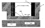
このようにして、あらかじめ選択されたまたは所望のパターン要素がPDMS成形スタンプ16の薄い隔膜部の外側表面に作られる。成形は、動作制御および空気圧の適切な手段に正しい位置で取り付けることができるように構成された構造と一体となって形成される。柔軟な隔膜部20は、たとえば管部材14の反対側の末端に適用された空気圧により容易に移動可能な程度に薄い。スタンプ16が、図1または2aに示されるように、隣接した位置に隔膜部20が基板12の表面18の近くに隣接するように位置する場合、管部材14の導管22を通して隔膜部20に気体の圧力を適用すると、隔膜が上記表面に向かって外側に移動し、図2bに示すように基板12の表面18と接触する。
In this way, a preselected or desired pattern element is created on the outer surface of the thin diaphragm portion of the
図3は、基板表面18と接触している外側にバイアスをかけられた隔膜20の拡大した詳細図である。薄膜部分20は基板の表面に非常に近接(〜0.001”)させなければならない。管14の内側におよそ60 psiの正の圧力をかけて、薄いポリマーフィルム部分20を風船のように膨らませる。この風船効果により、薄いポリマーフィルムのパターン化された/インクを付けた表面20はその膨らませていない位置と基板の表面の間の間隙を閉じることができる。柔軟性のある薄膜部分20は基板12の表面18と緊密に接触し、それにより被検体特異的受容体のパターンを基板の表面上に堆積する。パターン転移の前に薄膜部分20を基板12の表面18の非常に近くに持って来ることにより、基板と接触させるために非常に大きい伸長は必要ないので、パターンがゆがむことがない。そのため、接触が達成された後、隔膜部20により基板表面18に加えられた力は、接触領域全体に渡って本質的に均一である。この方法により線上および角度の両方の変位を調整することができる。この方法によりいくらかのパターンの歪みが生じるが、隔膜と基板の間の間隙が隔膜部20の直径と比較して小さければ、この歪みは小さく、したがって多くの応用において許容し得るものであり、また比較的予測可能である。スタンプを押すプロセスが完了した後に、圧力を解除するか、図4に示されるように、薄膜部分20を基板12の表面18から分離するために管の内部に負圧を適用するかのいずれかをおこなう。
FIG. 3 is an enlarged detail view of the outwardly
上記の大きさおよび圧力は単に例示であって、限定的な条件であると解釈される意味ではないことは当業者に理解されるであろう。60 psiよりもかなり低いまたは高い接触力および初期接近を使用してもよい。たとえば、スタンプと基板の初期接近の好ましい非限定的な範囲は、約0.0005”〜約0.005”であり、使用される好ましい非限定的な圧力の範囲は5 psi〜100 psi以上である。 Those skilled in the art will appreciate that the above magnitudes and pressures are merely exemplary and are not meant to be construed as limiting conditions. Much lower or higher contact force and initial approach than 60 psi may be used. For example, a preferred non-limiting range for the initial approach of the stamp and substrate is about 0.0005 "to about 0.005", and a preferred non-limiting pressure range used is 5 psi to 100 psi or more.
本発明のスタンプ装置を用いて作成されるパターンは、規則正しい等間隔の平行な線であってもよいし、または同時係属の米国特許出願番号09/814,161および10/242,778(これら両方の全体を参照により本明細書に組み入れる)において論じられるようなより複雑なパターンであってもよい。 The pattern created using the stamp device of the present invention may be regularly spaced parallel lines or co-pending US patent application Ser. Nos. 09 / 814,161 and 10 / 242,778 (see both in their entirety). May be more complex patterns as discussed in the present specification.
本発明のマイクロコンタクトプリンティングスタンプ10には、非常に厳格な大きさおよび位置の制御を必要としないという利点、および容易に制御され、繰り返し可能な、パターンの要素への接触力が得られるという利点がある。スタンプ表面のパターン要素の基板に対する回転方向の位置決定は、鍵となる基準の形を用いて、または当業者には明白な他の方法により決められる。角度および軸上の距離の許容性は、Tecan Genesis RSPまたはBeckman FX Laboratory Workstationなどの標準的な実験室用ロボット流体操作装置を含む容易に入手できる動作制御装置の使用が可能な程度に緩和されたものである。これにより、既成部品から、または比較的安価な注文の設備の設計および製造により、容易に組み立てることができる低コストのシステムが可能になる。
The
上記の構造のさらに別の利点は、回転方向および印刷される表面のx-y平面においてスタンプを正確に位置合わせする能力である。しばしば、特に回折光学素子センサーを使用する場合に上記の位置合わせは非常に重要である。硬質支持部材を基準とする印刷スタンプがない場合には、スタンプを基板に対して位置合わせし、そろえるための唯一の有効な方法は、パターン認識によるもの、または視覚的な顕微鏡の使用などの他の光学的手段によるものである。このような手段を使用した場合、接触面への視覚的アクセスを可能にする装置を作らなくてはならず、スタンプを回転および平行移動するために正確で調節可能な機械的手段を使用しなければならない。これらの要求のために、必要な装置にかかる費用が増大し、また、基板の形状のタイプが可視化および装置に接近することができるものに限定される可能性がある。 Yet another advantage of the above structure is the ability to accurately align the stamp in the direction of rotation and the xy plane of the printed surface. Often, the above alignment is very important, especially when using diffractive optical element sensors. In the absence of a printed stamp referenced to a rigid support member, the only effective method for aligning and aligning the stamp with the substrate is by pattern recognition or other such as using a visual microscope. This is due to optical means. If such means are used, a device must be made that allows visual access to the contact surface, and accurate and adjustable mechanical means must be used to rotate and translate the stamp. I must. These requirements increase the cost of the required equipment and may limit the type of substrate shape to one that can be visualized and accessed to the equipment.
本発明において、印刷スタンプは硬質支持部材の一方の末端に取り付けられる。この硬質支持部材は、種々の正確な物理的特性を有するように製造される。印刷スタンプを作成するプロセス中に、上記の硬質支持部材の物理的特性は、上記の部材とパターン形状を有するマスターとの間の正確な照合を確立するために使用される。固定具は基板を支持し、それを硬質支持部材に正確に照合するために使用される。硬質支持部材および固定具の粗い組み立てにより、印刷スタンプは、印刷スタンプの表面が基板の表面に平行になるように、またパターンの形状が基板に回転方向で照合するように、基板に非常に近接した位置に置かれる。 In the present invention, the printing stamp is attached to one end of the rigid support member. This rigid support member is manufactured to have a variety of precise physical properties. During the process of creating a print stamp, the physical properties of the rigid support member are used to establish an accurate match between the member and a master having a pattern shape. The fixture is used to support the substrate and accurately match it to the rigid support member. Due to the rough assembly of the rigid support members and fixtures, the printing stamp is very close to the substrate so that the surface of the printing stamp is parallel to the surface of the substrate and the shape of the pattern matches the rotation direction of the substrate. Placed in the position.
隔膜20および支持構造14をより精巧に設計することによりパターンの小さい歪みさえも最小化または排除することができることが当業者に理解されるであろう。たとえば、パターン領域の外側の周辺領域の隔膜の厚みを小さくすることにより、周辺領域がより大きい程度まで膨らんで要求される移動に対応するので、パターン領域の歪みが減少する。あるいは、同じ結果を得るためにパターン領域を厚くすることもできる。Marsh-Bellofram社により採用されているものと同様の回転隔膜設計を取り入れることにより、基本的にパターン領域のすべての歪みを排除することが可能になる。
It will be appreciated by those skilled in the art that even a small distortion of the pattern can be minimized or eliminated by more elaborately designing the
本発明の別の利点は、低コストの使い捨ての器具への適合が容易である点である。不可欠の隔膜20を有するPDMSスタンプ16は、公知の技術を用いて支持体14の周りにインサート成型されてもよい。この組み立ては、位置に関する許容誤差の要求が緩和されるために可能となる。図3を参照すると、標準的または修正された実験室用ロボット流体操作装置と共に使用するのに適した、硬質支持構造14および弾力のある柔軟なスタンプ16を含むスタンプ集合体30の列を使用することができる。支持構造14は、好ましくは好適な特性を有する多くのポリマーを射出成形したものであるが、金属などの他の材料もまた使用できると理解される。
Another advantage of the present invention is that it is easy to adapt to low cost disposable instruments. The
本発明のパターン堆積システム(PDS)は、基板の表面上にパターンを堆積するための標準化された方法を有利に提供する。それは、かなりの堆積圧力、温度、湿度、動作速度、スタンプシーケンス、および位置パラメーターの名目上の変位を最小化する。それは容易に運搬できる装置を提供する。 The pattern deposition system (PDS) of the present invention advantageously provides a standardized method for depositing patterns on the surface of a substrate. It minimizes the nominal displacement of significant deposition pressure, temperature, humidity, operating speed, stamp sequence, and position parameters. It provides an easily transportable device.
本明細書において、「含む」という用語は、包含するが制限がなく、排他的ではないと解釈される。特に、請求の範囲を含む本明細書において使用される場合、「含む」およびその変形は特定された特徴、段階または構成要素が含まれることを意味する。この用語は他の特徴、段階または構成要素の存在を排除するとは解釈されない。 As used herein, the term “comprising” is to be interpreted as being inclusive but not limiting and exclusive. In particular, as used in this specification, including the claims, "includes" and variations thereof mean that the specified features, steps or components are included. This term is not to be interpreted as excluding the presence of other features, steps or components.
前記の本発明の好ましい実施形態の説明は本発明の原理を説明するために提供されたものであり、例示された特定の実施形態に発明を限定するものではない。本発明の範囲は、特許請求の範囲およびそれと同等のものに包含されるすべての実施形態により定義されることが意図されている。 The foregoing description of the preferred embodiment of the invention has been provided to illustrate the principles of the invention and is not intended to limit the invention to the particular embodiment illustrated. It is intended that the scope of the invention be defined by all embodiments encompassed by the claims and their equivalents.
上記の説明は、添付した図面を参照して、本発明のマイクロコンタクトプリンティングの方法および装置について、例としての目的のみで提供するものである。 The foregoing description provides, by way of example only, the microcontact printing method and apparatus of the present invention with reference to the accompanying drawings.
図2bは、加圧されたハウジングの内部を有するハウジングの末端に取り付けられたポリマースタンプの横断面図である。
Claims (18)
上記硬質支持部材の第1の反対側の末端に取り付けられた印刷スタンプであって、上記印刷スタンプは柔軟な隔膜部である部分を有し、上記柔軟な隔膜部は1種以上の材料によりあらかじめ選択されたパターンに被覆された外側表面を有するもの;および
柔軟な隔膜部に外側にバイアスをかけてこれを基板の表面と緊密かつ実質的に均一に接触させ、1種以上の材料のあらかじめ選択されたパターンを上記表面上に転移させるための、流体流路を通じて柔軟な隔膜部の内側表面と連絡しているバイアス手段
を含む、基板の表面にパターンを作成するための装置。 A rigid support member having first and second opposite ends and a fluid flow path extending therethrough;
A printing stamp attached to the first opposite end of the rigid support member, wherein the printing stamp has a portion that is a flexible diaphragm portion, and the flexible diaphragm portion is preliminarily made of one or more materials. Having an outer surface coated with a selected pattern; and pre-selecting one or more materials by biasing the flexible diaphragm portion outward to bring it into intimate and substantially uniform contact with the surface of the substrate An apparatus for creating a pattern on the surface of a substrate, comprising biasing means in fluid communication with the inner surface of the flexible diaphragm through the fluid flow path for transferring the patterned pattern onto the surface.
Applications Claiming Priority (2)
| Application Number | Priority Date | Filing Date | Title |
|---|---|---|---|
| US10/744,949 US6981445B2 (en) | 2003-12-24 | 2003-12-24 | Method and apparatus for micro-contact printing |
| PCT/CA2004/002175 WO2005061237A1 (en) | 2003-12-24 | 2004-12-22 | Method and apparatus for micro-contact printing |
Publications (2)
| Publication Number | Publication Date |
|---|---|
| JP2007516869A true JP2007516869A (en) | 2007-06-28 |
| JP2007516869A5 JP2007516869A5 (en) | 2007-10-25 |
Family
ID=34700532
Family Applications (1)
| Application Number | Title | Priority Date | Filing Date |
|---|---|---|---|
| JP2006545865A Pending JP2007516869A (en) | 2003-12-24 | 2004-12-22 | Method and apparatus for microcontact printing |
Country Status (8)
| Country | Link |
|---|---|
| US (1) | US6981445B2 (en) |
| EP (1) | EP1701849A1 (en) |
| JP (1) | JP2007516869A (en) |
| KR (1) | KR101198500B1 (en) |
| CN (1) | CN100540320C (en) |
| CA (1) | CA2541239C (en) |
| MX (1) | MXPA06007383A (en) |
| WO (1) | WO2005061237A1 (en) |
Families Citing this family (27)
| Publication number | Priority date | Publication date | Assignee | Title |
|---|---|---|---|---|
| US6939120B1 (en) * | 2002-09-12 | 2005-09-06 | Komag, Inc. | Disk alignment apparatus and method for patterned media production |
| US7114448B2 (en) * | 2003-11-06 | 2006-10-03 | Palo Alto Research Center, Incorporated | Method for large-area patterning dissolved polymers by making use of an active stamp |
| ATE396048T1 (en) * | 2004-12-10 | 2008-06-15 | Essilor Int | STAMP FOR APPLYING A MOTIF, METHOD FOR PRODUCING STAMPS AND METHOD FOR PRODUCING AN OBJECT USING THIS STAMP |
| US7491423B1 (en) | 2005-05-02 | 2009-02-17 | Sandia Corporation | Directed spatial organization of zinc oxide nanostructures |
| PL1890887T3 (en) * | 2005-05-03 | 2016-04-29 | Koninklijke Philips Nv | Method and device for transferring a pattern from a stamp to a substrate |
| JP4449949B2 (en) * | 2006-07-18 | 2010-04-14 | セイコーエプソン株式会社 | Surface energy difference bank forming method, pattern forming method, bank structure, electronic circuit, electronic device, electronic apparatus, and stamp |
| US20080083484A1 (en) * | 2006-09-28 | 2008-04-10 | Graciela Beatriz Blanchet | Method to form a pattern of functional material on a substrate |
| EP2092340B1 (en) | 2006-10-18 | 2014-07-09 | Axela Inc. | Measuring multiple analytes over a broad range of concentrations using optical diffraction |
| WO2008115530A2 (en) * | 2007-03-20 | 2008-09-25 | Nano Terra Inc. | Polymer composition for preparing electronic devices by microcontact printing processes and products prepared by the processes |
| DE112008001634A5 (en) * | 2007-06-21 | 2010-04-01 | GeSIM Gesellschaft für Silizium-Mikrosysteme mbH | Method and device for transfer of micro- or nanostructures by contact stamping |
| US20090025595A1 (en) * | 2007-07-25 | 2009-01-29 | Nano Terra Inc. | Contact Printing Method Using an Elastomeric Stamp Having a Variable Surface Area and Variable Shape |
| EP2217694A4 (en) | 2007-11-13 | 2011-08-31 | Univ California | Processes for rapid microfabrication using thermoplastics and devices thereof |
| US8338189B2 (en) | 2008-03-05 | 2012-12-25 | Axela Inc. | Detection of biomarkers and biomarker complexes |
| US20110052549A1 (en) * | 2009-08-27 | 2011-03-03 | The Regents Of The University Of California | Cell culture device to differentiate stem cells in a specific orientation |
| KR101790367B1 (en) | 2009-12-22 | 2017-10-25 | 쓰리엠 이노베이티브 프로퍼티즈 컴파니 | Apparatus and method for microcontact printing using a pressurized roller |
| GB201009621D0 (en) | 2010-06-09 | 2010-07-21 | Laja Materials Ltd | Stamping apparatus |
| US8449285B2 (en) * | 2011-01-21 | 2013-05-28 | Hepregen Corporation | Systems and methods for micro-contact stamping |
| KR101967015B1 (en) * | 2011-09-16 | 2019-04-08 | 쓰리엠 이노베이티브 프로퍼티즈 캄파니 | Method and apparatus for applying a stamp for micro-contact printing to a stamping roll |
| US9149958B2 (en) | 2011-11-14 | 2015-10-06 | Massachusetts Institute Of Technology | Stamp for microcontact printing |
| US9266260B2 (en) | 2011-12-20 | 2016-02-23 | Massachusetts Institute Of Technology | Precision continuous stamp casting method for roll-based soft lithography |
| CN102616031B (en) * | 2012-03-29 | 2014-01-29 | 浙江大学 | Magnetic force controlled ink permeating type micro-contact printing device |
| KR101955335B1 (en) | 2012-11-14 | 2019-03-07 | 삼성전자주식회사 | Stamp structure and transfer method using the same |
| US9434150B2 (en) * | 2014-07-20 | 2016-09-06 | X-Celeprint Limited | Apparatus and methods for micro-transfer-printing |
| CN107215111B (en) * | 2017-06-14 | 2023-03-28 | 浙江大学 | Magnetic control transfer seal and magnetic control transfer printing method |
| KR102094005B1 (en) * | 2018-05-29 | 2020-03-27 | 한밭대학교 산학협력단 | Micro-contact printing system using roll to roll process |
| US10748793B1 (en) | 2019-02-13 | 2020-08-18 | X Display Company Technology Limited | Printing component arrays with different orientations |
| CN113433062B (en) * | 2021-06-15 | 2022-07-08 | 清华大学 | Method and device for testing joint force between stamp unit and sample |
Citations (1)
| Publication number | Priority date | Publication date | Assignee | Title |
|---|---|---|---|---|
| JPS5389503A (en) * | 1977-01-17 | 1978-08-07 | Honda Motor Co Ltd | Method of and device for printing on curved surface |
Family Cites Families (13)
| Publication number | Priority date | Publication date | Assignee | Title |
|---|---|---|---|---|
| US3756165A (en) | 1972-05-22 | 1973-09-04 | Interpace Corp | Method for printing on ceramic tableware |
| US5512131A (en) | 1993-10-04 | 1996-04-30 | President And Fellows Of Harvard College | Formation of microstamped patterns on surfaces and derivative articles |
| US6180239B1 (en) | 1993-10-04 | 2001-01-30 | President And Fellows Of Harvard College | Microcontact printing on surfaces and derivative articles |
| US5669303A (en) | 1996-03-04 | 1997-09-23 | Motorola | Apparatus and method for stamping a surface |
| US5731152A (en) * | 1996-05-13 | 1998-03-24 | Motorola, Inc. | Methods and systems for biological reagent placement |
| US5937758A (en) * | 1997-11-26 | 1999-08-17 | Motorola, Inc. | Micro-contact printing stamp |
| US5947027A (en) | 1998-09-08 | 1999-09-07 | Motorola, Inc. | Printing apparatus with inflatable means for advancing a substrate towards the stamping surface |
| US6221579B1 (en) * | 1998-12-11 | 2001-04-24 | Kimberly-Clark Worldwide, Inc. | Patterned binding of functionalized microspheres for optical diffraction-based biosensors |
| EP1297387A2 (en) | 2000-06-30 | 2003-04-02 | President And Fellows of Harvard College | Electric microcontact printing method and apparatus |
| AU2001284896A1 (en) * | 2000-08-14 | 2002-02-25 | Surface Logix, Inc. | Deformable stamp for patterning three-dimensional surfaces |
| US20020130444A1 (en) | 2001-03-15 | 2002-09-19 | Gareth Hougham | Post cure hardening of siloxane stamps for microcontact printing |
| US7338613B2 (en) | 2001-09-10 | 2008-03-04 | Surface Logix, Inc. | System and process for automated microcontact printing |
| WO2003065120A2 (en) | 2002-01-11 | 2003-08-07 | Massachusetts Institute Of Technology | Microcontact printing |
-
2003
- 2003-12-24 US US10/744,949 patent/US6981445B2/en not_active Expired - Fee Related
-
2004
- 2004-12-22 WO PCT/CA2004/002175 patent/WO2005061237A1/en active Application Filing
- 2004-12-22 EP EP04802350A patent/EP1701849A1/en not_active Withdrawn
- 2004-12-22 CA CA002541239A patent/CA2541239C/en not_active Expired - Fee Related
- 2004-12-22 KR KR1020067014463A patent/KR101198500B1/en not_active IP Right Cessation
- 2004-12-22 MX MXPA06007383A patent/MXPA06007383A/en active IP Right Grant
- 2004-12-22 CN CNB2004800387574A patent/CN100540320C/en not_active Expired - Fee Related
- 2004-12-22 JP JP2006545865A patent/JP2007516869A/en active Pending
Patent Citations (1)
| Publication number | Priority date | Publication date | Assignee | Title |
|---|---|---|---|---|
| JPS5389503A (en) * | 1977-01-17 | 1978-08-07 | Honda Motor Co Ltd | Method of and device for printing on curved surface |
Also Published As
| Publication number | Publication date |
|---|---|
| CN100540320C (en) | 2009-09-16 |
| CN1898091A (en) | 2007-01-17 |
| CA2541239C (en) | 2009-06-09 |
| KR20070019969A (en) | 2007-02-16 |
| US6981445B2 (en) | 2006-01-03 |
| MXPA06007383A (en) | 2007-01-26 |
| WO2005061237A1 (en) | 2005-07-07 |
| US20050139103A1 (en) | 2005-06-30 |
| CA2541239A1 (en) | 2005-07-07 |
| EP1701849A1 (en) | 2006-09-20 |
| KR101198500B1 (en) | 2012-11-06 |
Similar Documents
| Publication | Publication Date | Title |
|---|---|---|
| JP2007516869A (en) | Method and apparatus for microcontact printing | |
| JP2007516869A5 (en) | ||
| JP3958344B2 (en) | Imprint apparatus, imprint method, and chip manufacturing method | |
| US9440254B2 (en) | Method and apparatus for applying a sheet to a substrate | |
| EP1497102B1 (en) | Device and method for transferring a pattern to a substrate | |
| US7830498B2 (en) | Hydraulic-facilitated contact lithography apparatus, system and method | |
| KR20080059547A (en) | Contact lithography apparatus, system and method | |
| US20120193832A1 (en) | Holding apparatus, imprint apparatus and article manufacturing method using same | |
| JP6497839B2 (en) | Imprint apparatus and article manufacturing method | |
| CN109952537B (en) | Positioning a substrate in an imprint lithography process | |
| JP6391709B2 (en) | Method and apparatus for embossing nanostructures | |
| JP4640512B2 (en) | Pattern forming apparatus and method | |
| US20230229076A1 (en) | Method and device for producing micro- and/or nanostructures | |
| JP7419516B2 (en) | Apparatus and method for embossing micropatterns and/or nanopatterns | |
| JP2016021443A (en) | Imprint device and article manufacturing method | |
| JP5224930B2 (en) | Transfer device | |
| JP2007320113A (en) | Equipment and method for forming pattern | |
| SE524563C2 (en) | Micro or nanostructures transferring device for lithography, has two stamping plates that are bendable towards each other while being secured to each other at respective holding areas |
Legal Events
| Date | Code | Title | Description |
|---|---|---|---|
| A521 | Written amendment |
Free format text: JAPANESE INTERMEDIATE CODE: A523 Effective date: 20070904 |
|
| A621 | Written request for application examination |
Free format text: JAPANESE INTERMEDIATE CODE: A621 Effective date: 20070904 |
|
| A131 | Notification of reasons for refusal |
Free format text: JAPANESE INTERMEDIATE CODE: A131 Effective date: 20110104 |
|
| A02 | Decision of refusal |
Free format text: JAPANESE INTERMEDIATE CODE: A02 Effective date: 20111213 |