JP2007513381A - Light source using a plurality of LEDs and method of assembling the light source - Google Patents
Light source using a plurality of LEDs and method of assembling the light source Download PDFInfo
- Publication number
- JP2007513381A JP2007513381A JP2006542584A JP2006542584A JP2007513381A JP 2007513381 A JP2007513381 A JP 2007513381A JP 2006542584 A JP2006542584 A JP 2006542584A JP 2006542584 A JP2006542584 A JP 2006542584A JP 2007513381 A JP2007513381 A JP 2007513381A
- Authority
- JP
- Japan
- Prior art keywords
- light
- layer
- led
- phosphor
- light source
- Prior art date
- Legal status (The legal status is an assumption and is not a legal conclusion. Google has not performed a legal analysis and makes no representation as to the accuracy of the status listed.)
- Withdrawn
Links
Images


Classifications
-
- G—PHYSICS
- G02—OPTICS
- G02B—OPTICAL ELEMENTS, SYSTEMS OR APPARATUS
- G02B6/00—Light guides; Structural details of arrangements comprising light guides and other optical elements, e.g. couplings
- G02B6/24—Coupling light guides
- G02B6/42—Coupling light guides with opto-electronic elements
-
- G—PHYSICS
- G02—OPTICS
- G02B—OPTICAL ELEMENTS, SYSTEMS OR APPARATUS
- G02B6/00—Light guides; Structural details of arrangements comprising light guides and other optical elements, e.g. couplings
- G02B6/24—Coupling light guides
- G02B6/42—Coupling light guides with opto-electronic elements
- G02B6/4201—Packages, e.g. shape, construction, internal or external details
- G02B6/4249—Packages, e.g. shape, construction, internal or external details comprising arrays of active devices and fibres
-
- F—MECHANICAL ENGINEERING; LIGHTING; HEATING; WEAPONS; BLASTING
- F21—LIGHTING
- F21K—NON-ELECTRIC LIGHT SOURCES USING LUMINESCENCE; LIGHT SOURCES USING ELECTROCHEMILUMINESCENCE; LIGHT SOURCES USING CHARGES OF COMBUSTIBLE MATERIAL; LIGHT SOURCES USING SEMICONDUCTOR DEVICES AS LIGHT-GENERATING ELEMENTS; LIGHT SOURCES NOT OTHERWISE PROVIDED FOR
- F21K9/00—Light sources using semiconductor devices as light-generating elements, e.g. using light-emitting diodes [LED] or lasers
- F21K9/60—Optical arrangements integrated in the light source, e.g. for improving the colour rendering index or the light extraction
- F21K9/68—Details of reflectors forming part of the light source
-
- G—PHYSICS
- G02—OPTICS
- G02B—OPTICAL ELEMENTS, SYSTEMS OR APPARATUS
- G02B6/00—Light guides; Structural details of arrangements comprising light guides and other optical elements, e.g. couplings
- G02B6/24—Coupling light guides
- G02B6/42—Coupling light guides with opto-electronic elements
- G02B6/4201—Packages, e.g. shape, construction, internal or external details
- G02B6/4204—Packages, e.g. shape, construction, internal or external details the coupling comprising intermediate optical elements, e.g. lenses, holograms
- G02B6/4214—Packages, e.g. shape, construction, internal or external details the coupling comprising intermediate optical elements, e.g. lenses, holograms the intermediate optical element having redirecting reflective means, e.g. mirrors, prisms for deflecting the radiation from horizontal to down- or upward direction toward a device
-
- G—PHYSICS
- G02—OPTICS
- G02B—OPTICAL ELEMENTS, SYSTEMS OR APPARATUS
- G02B6/00—Light guides; Structural details of arrangements comprising light guides and other optical elements, e.g. couplings
- G02B6/24—Coupling light guides
- G02B6/42—Coupling light guides with opto-electronic elements
- G02B6/43—Arrangements comprising a plurality of opto-electronic elements and associated optical interconnections
-
- G—PHYSICS
- G02—OPTICS
- G02B—OPTICAL ELEMENTS, SYSTEMS OR APPARATUS
- G02B6/00—Light guides; Structural details of arrangements comprising light guides and other optical elements, e.g. couplings
- G02B6/24—Coupling light guides
- G02B6/36—Mechanical coupling means
- G02B6/3628—Mechanical coupling means for mounting fibres to supporting carriers
- G02B6/3632—Mechanical coupling means for mounting fibres to supporting carriers characterised by the cross-sectional shape of the mechanical coupling means
- G02B6/3644—Mechanical coupling means for mounting fibres to supporting carriers characterised by the cross-sectional shape of the mechanical coupling means the coupling means being through-holes or wall apertures
-
- G—PHYSICS
- G02—OPTICS
- G02B—OPTICAL ELEMENTS, SYSTEMS OR APPARATUS
- G02B6/00—Light guides; Structural details of arrangements comprising light guides and other optical elements, e.g. couplings
- G02B6/24—Coupling light guides
- G02B6/36—Mechanical coupling means
- G02B6/3628—Mechanical coupling means for mounting fibres to supporting carriers
- G02B6/3664—2D cross sectional arrangements of the fibres
- G02B6/3672—2D cross sectional arrangements of the fibres with fibres arranged in a regular matrix array
-
- G—PHYSICS
- G02—OPTICS
- G02B—OPTICAL ELEMENTS, SYSTEMS OR APPARATUS
- G02B6/00—Light guides; Structural details of arrangements comprising light guides and other optical elements, e.g. couplings
- G02B6/24—Coupling light guides
- G02B6/42—Coupling light guides with opto-electronic elements
- G02B6/4298—Coupling light guides with opto-electronic elements coupling with non-coherent light sources and/or radiation detectors, e.g. lamps, incandescent bulbs, scintillation chambers
Abstract
光源は、複数の発光ダイオード(LED)(102、206、306、626)を用いて形成される。LEDによって発せられた光に対して透過性である材料の第1の層(220、320)は、複数のLEDの上に配置される。光は、材料の第1の層を通って、LEDから第1の層の他方の側の上に配置される蛍光体層(218、318)に伝搬する。光は、広帯域の白色光を生成するために、蛍光体で変換される。材料の第1の層(220、320)は、変換された光の波長で反射してもよく、LED(106、206、306、626)に向かって戻るように伝搬する変換光は前方方向に反射される。蛍光体材料は、第1の層(220、320)上のパッチとして形成されてもよい。反射結合器などの結合器(210、310、604)のアレイは、各LED(102、206、306、626)によって生成された波長変換光をそれぞれの光ファイバ(106)に結合するために用いられてもよい。 The light source is formed using a plurality of light emitting diodes (LEDs) (102, 206, 306, 626). A first layer (220, 320) of material that is transparent to the light emitted by the LEDs is disposed over the plurality of LEDs. Light propagates through the first layer of material from the LED to the phosphor layer (218, 318) disposed on the other side of the first layer. The light is converted with a phosphor to produce broadband white light. The first layer of material (220, 320) may reflect at the wavelength of the converted light, and the converted light propagating back toward the LEDs (106, 206, 306, 626) will be forward. Reflected. The phosphor material may be formed as a patch on the first layer (220, 320). An array of couplers (210, 310, 604), such as reflective couplers, is used to couple the wavelength converted light generated by each LED (102, 206, 306, 626) to a respective optical fiber (106). May be.
Description
本発明は、光学系に関し、さらに詳細には複数の光源の利用に基づく照射システムに適用可能である。 The present invention relates to an optical system, and more particularly to an illumination system based on the use of a plurality of light sources.
照射システムは、種々の用途に用いられる。住宅、医療、歯科および産業用途では、光を利用することが必要な場合が多い。同様に、航空機、船舶および自動車の用途では、高強度の照射ビームを必要とすることが多い。従来の照明システムは、電気によって出力されるフィラメントまたはアーク灯を用いてきた。これらの照明システムは、生成された照射光をビームとして向けるために、合焦レンズおよび/または反射面を備えることがよくある。しかし、スイミングプールの照明などの一定の用途において、最終的な光出力を電気的接触が望ましくない環境に配置する必要がある場合がある。自動車の前照灯などの他の用途では、光源を露出された損傷を受けやすい位置からより安全な位置に移動するという要望がある。また、さらに別の用途では、物理的空間の制限、接近可能性または設計などの考慮事項から、最終的な照射が必要される場所とは異なる位置に光源を配置することが必要となる場合がある。 Irradiation systems are used for various applications. In residential, medical, dental and industrial applications, it is often necessary to use light. Similarly, aircraft, marine and automotive applications often require high intensity illumination beams. Conventional lighting systems have used filaments or arc lamps that are output by electricity. These illumination systems often include a focusing lens and / or a reflective surface to direct the generated illumination light as a beam. However, in certain applications, such as swimming pool lighting, the final light output may need to be placed in an environment where electrical contact is undesirable. In other applications, such as automotive headlamps, there is a desire to move the light source from an exposed, vulnerable location to a safer location. In yet another application, considerations such as physical space limitations, accessibility, or design may require that the light source be located at a location different from where final illumination is required. is there.
これらの必要性の一部に対して、光導波路を用いて光源からの光を所望の照射点まで案内する照射システムが開発されている。1つの現行の手法は、1つの明るい光源または共に集められて1つの照射源を形成する一連の光源のいずれかを用いることである。そのような光源によって発せられた光は、合焦光学素子を用いて、1つまたは複数の光源から離れた位置に光を伝送する大口径プラスチックファイバなどの1つの光導波路に向けられる。さらに別の手法では、単一ファイバを個別の光ファイバの束に置き換えてもよい。 In response to some of these needs, an irradiation system has been developed that guides light from a light source to a desired irradiation point using an optical waveguide. One current approach is to use either one bright light source or a series of light sources that are gathered together to form one illumination source. The light emitted by such a light source is directed to a single optical waveguide, such as a large diameter plastic fiber, that transmits the light away from the one or more light sources using focusing optics. In yet another approach, a single fiber may be replaced with a bundle of individual optical fibers.
現行の方法は、場合によっては生成された光の約70%が失われるため、非効率的である。多重ファイバシステムでは、これらの損失は、束になったファイバ間の暗い間隙空間およびファイバ束に光を向ける非効率性に起因する恐れがある。単一のファイバシステムでは、明るい照明用途に必要な光の量を捕捉するほど十分に大きな直径を有する単一ファイバは重くなりすぎ、経路指定および小さな半径に曲げることに対する自由度が失われる。 Current methods are inefficient because in some cases about 70% of the generated light is lost. In multi-fiber systems, these losses can be due to the dark gap space between the bundled fibers and the inefficiency of directing light to the fiber bundle. In a single fiber system, a single fiber with a sufficiently large diameter to capture the amount of light required for bright lighting applications becomes too heavy and loses the freedom to route and bend to a small radius.
一部の光生成システムは、光源としてレーザを用い、可干渉の光出力を活かしている。しかし、レーザ光源は通常は単一の出力色を生成するのに対し、照射システムは通常は、より広帯域の白色光源を必要とする。さらに、レーザダイオードは一般に、非対称のビーム形状を有する光を生成するため、光ファイバへの効率的な結合を達成するために、光学ビーム整形素子を多数使用することが必要である。さらに、一部のレーザダイオードは、動作中に生成する熱のために、厳密な温度制御を必要とすることから(たとえば、熱電冷却器などを用いる必要がある)、利用にはコストが嵩む。 Some light generation systems use a laser as a light source and take advantage of coherent light output. However, while laser light sources typically produce a single output color, illumination systems typically require a broader white light source. In addition, laser diodes generally produce light having an asymmetric beam shape, and so it is necessary to use a number of optical beam shaping elements to achieve efficient coupling to the optical fiber. In addition, some laser diodes require strict temperature control due to the heat generated during operation (eg, it is necessary to use a thermoelectric cooler or the like), which is expensive to use.
したがって、効率的かつ廉価で光を生成し、遠隔照射に用いることができる光源に関する継続的需要が依然としてある。 Thus, there remains a continuing need for light sources that can generate light efficiently and inexpensively and that can be used for remote illumination.
本発明の1つの特定の実施形態は、LED光を発することができる発光ダイオード(LED)ダイおよびそれぞれのLEDダイからの光を結合するための光結合器を備える光源に関する。蛍光体パッチは、LEDダイと光結合器との間に配置され、それぞれのLEDダイから光結合器に伝搬するLED光の少なくとも一部を変換する。中間層が、LEDダイと蛍光体パッチとの間に配置される。中間層は、LED光を透過し、蛍光体パッチで変換される光を反射する。中間層は、LEDダイに面する第1の側および結合器に面する第2の側を有する。蛍光体パッチは、中間層の第2の側に配置される。LED光は、青色光または紫外光であってもよい。 One particular embodiment of the present invention relates to a light source comprising a light emitting diode (LED) die capable of emitting LED light and an optical combiner for combining light from each LED die. The phosphor patch is disposed between the LED die and the optical coupler and converts at least a portion of the LED light propagating from the respective LED die to the optical coupler. An intermediate layer is disposed between the LED die and the phosphor patch. The intermediate layer transmits LED light and reflects light converted by the phosphor patch. The intermediate layer has a first side facing the LED die and a second side facing the coupler. The phosphor patch is disposed on the second side of the intermediate layer. The LED light may be blue light or ultraviolet light.
本発明の別の実施形態は、LED光を生成するための2つ以上の発光ダイオード(LED)ダイと、LEDダイからの光を結合するための2つ以上のそれぞれの結合器と、を含んで成る光源に関する。中間層が、LEDダイと結合器との間に配置される。中間層は、LED光に対して実質的に透明である。蛍光体層が、中間層と結合器との間で、中間層の上に配置され、LED光の少なくとも一部を変換された波長の光に変換する。 Another embodiment of the present invention includes two or more light emitting diode (LED) dies for generating LED light, and two or more respective couplers for combining light from the LED dies. It is related with the light source which consists of. An intermediate layer is disposed between the LED die and the coupler. The intermediate layer is substantially transparent to the LED light. A phosphor layer is disposed on the intermediate layer between the intermediate layer and the coupler and converts at least a portion of the LED light into converted wavelength light.
本発明の別の実施形態は、LED光を発することができる複数の発光ダイオード(LED)ダイと、LEDダイの上方に配置された第1の層と、を含んで成る光源に関する。第1の層は、LED光に対して実質的に透明である。LED光は、第1の層の中を第1の層の第1の側から第1の層の第2の側まで伝搬する。蛍光体層は、第1の層の第2の側の上に配置される。 Another embodiment of the invention is directed to a light source comprising a plurality of light emitting diode (LED) dies capable of emitting LED light and a first layer disposed above the LED dies. The first layer is substantially transparent to LED light. The LED light propagates in the first layer from the first side of the first layer to the second side of the first layer. The phosphor layer is disposed on the second side of the first layer.
本発明の別の実施形態は、光源を組み立てる方法に関する。この方法は、LED光を発することができる複数の発光ダイオード(LED)ダイを提供するステップを含む。蛍光体の層は第1の層の上に配置され、第1の層はLED光に対して実質的に透明である。第1の層および蛍光体の層はLEDダイの上方に位置決めされ、LED光は第1の層を通ってLEDダイから蛍光体の層に伝搬する。 Another embodiment of the invention relates to a method for assembling a light source. The method includes providing a plurality of light emitting diode (LED) dies that can emit LED light. The phosphor layer is disposed on the first layer, and the first layer is substantially transparent to the LED light. The first layer and the phosphor layer are positioned above the LED die, and the LED light propagates from the LED die to the phosphor layer through the first layer.
本発明の上記の概要は、本発明のそれぞれの示された実施形態またはすべての実装例を説明することを目的としていない。図面および以下の詳細な説明は、これらの実施形態をさらに詳細に具体化している。 The above summary of the present invention is not intended to describe each illustrated embodiment or every implementation of the present invention. The drawings and the following detailed description embody these embodiments in more detail.
本発明は、添付図面と共に、本発明の種々の実施形態に関する以下の詳細な説明を検討すれば、より完全に理解されるであろう。 The invention will be more fully understood upon consideration of the following detailed description of various embodiments of the invention in conjunction with the accompanying drawings.
本発明は種々の変更および代替形態に適用可能であるが、その詳細が図に一例として示され、詳細に説明される。しかし、記載された特定の実施形態に本発明を限定するわけではないことを理解すべきである。逆に言えば、添付の特許請求の範囲によって規定されるように、本発明の精神および範囲に包含されるすべての変更、代替および変形を包含するものとする。 While the invention is amenable to various modifications and alternative forms, specifics thereof have been shown by way of example in the drawings and will be described in detail. However, it should be understood that the invention is not limited to the specific embodiments described. On the contrary, it is intended to cover all modifications, alternatives, and variations encompassed within the spirit and scope of the invention as defined by the appended claims.
本発明は、光学系に適用可能であり、さらに詳細には、1つ以上の発光ダイオード(LED)の使用に基づく照射システムおよびそのようなシステムの製造方法に適用可能である。 The present invention is applicable to optical systems, and more particularly to illumination systems based on the use of one or more light emitting diodes (LEDs) and methods of manufacturing such systems.
より高い出力パワーを有するLEDがさらに容易に利用可能となりつつあり、白色光によるLED照射用の新たな用途を開拓している。高パワーLEDを用いて対応しうる用途の中には、投影およびディスプレイシステムにおける光源、マシンビジョンシステムおよびカメラ/ビデオ用途およびさらに自動車の前照灯など遠距離照明システムにおける照射源としての使用が挙げられる。LEDを用いて白色光を生成するために、異なる手法を用いてもよい。1つの手法は、異なる波長で光を発するLEDの組み合わせを用いることである。別の手法は、短波長、たとえばスペクトルの青色または近紫外(UV)部分で光を生成するLEDを用い、短波長光を可視スペクトルにおける他の波長に変換することである。結果として生じる光は、可視スペクトルの大部分に及び、本願明細書では広帯域光と呼ばれる。スペクトルの青色またはUV部分で光を発するLEDは、窒化ガリウム、炭化ケイ素または青色光またはUV光の生成に適したバンドギャップを有する他の半導体材料に基づいていてもよい。 LEDs with higher output power are becoming more readily available, pioneering new applications for LED illumination with white light. Among the applications that can be addressed using high power LEDs are use as light sources in projection and display systems, machine vision systems and camera / video applications, and also as illumination sources in long-distance lighting systems such as automotive headlamps. It is done. Different approaches may be used to generate white light using an LED. One approach is to use a combination of LEDs that emit light at different wavelengths. Another approach is to use LEDs that generate light at short wavelengths, such as the blue or near ultraviolet (UV) portion of the spectrum, and convert short wavelength light to other wavelengths in the visible spectrum. The resulting light spans the majority of the visible spectrum and is referred to herein as broadband light. LEDs that emit light in the blue or UV portion of the spectrum may be based on gallium nitride, silicon carbide, or other semiconductor materials having a band gap suitable for the generation of blue or UV light.
白色光は、人間の目における赤色センサ、緑色センサおよび青色センサを刺激する光であり、通常の観察者が「白色」とみなす外観を生じる。そのような白色光は、赤色(「温白色光」と一般に呼ばれる)に偏っているか、青色(「冷白色光」と一般に呼ばれる)に偏っていてもよい。そのような光は、100までの演色指数を有することができる。 White light is light that stimulates the red, green, and blue sensors in the human eye and produces an appearance that a normal observer considers to be “white”. Such white light may be biased red (commonly referred to as “warm white light”) or blue (commonly referred to as “cold white light”). Such light can have a color rendering index of up to 100.
より短い波長の光をより長い波長の光に変換するために用いられる材料は、本願明細書では「蛍光体」と呼ばれる。蛍光体は、より長い波長の光を生成するための異なる機構、たとえば、蛍光または燐光を用いてもよい。蛍光体は、無機、有機またはその両方の組み合わせであってもよい。無機蛍光体の例としては、ガーネット、ケイ酸塩および他のセラミックスが挙げられる。ガーネット蛍光体の具体的な例は、ガドリニウムをドープしたセリウム活性化イットリウムアルミニウムガーネット(Ce:YAG)である。他の蛍光種、たとえば、サマリウム、プラセオジムなどの希土類ドーパントを用いてもよい。有機蛍光体の例としては、有機蛍光材料、たとえば有機染料、顔料などが挙げられる。 The material used to convert shorter wavelength light into longer wavelength light is referred to herein as a “phosphor”. Phosphors may use different mechanisms for generating longer wavelength light, such as fluorescence or phosphorescence. The phosphor may be inorganic, organic or a combination of both. Examples of inorganic phosphors include garnet, silicate and other ceramics. A specific example of a garnet phosphor is cerium activated yttrium aluminum garnet (Ce: YAG) doped with gadolinium. Other fluorescent species, for example, rare earth dopants such as samarium and praseodymium may be used. Examples of organic phosphors include organic phosphor materials such as organic dyes and pigments.
蛍光体材料は一般に、約300nm〜約450nmの範囲の励起波長および可視波長範囲の発光波長を有する。狭い発光波長帯を有する蛍光体材料の場合には、蛍光体材料の混合物、たとえば、赤色発光蛍光体、緑色発光蛍光体および青色発光蛍光体からなる混合物を用いて配合し、視認者が視認した場合に、所望のカラーバランスを達成できる。より広い発光帯を有する蛍光体材料は、より高い演色指数を有する蛍光体混合物に適している。蛍光体は、高速放射遅延速度を有するものであることが望ましい。 The phosphor material generally has an excitation wavelength in the range of about 300 nm to about 450 nm and an emission wavelength in the visible wavelength range. In the case of a phosphor material having a narrow emission wavelength band, a mixture of phosphor materials, for example, a mixture of a red light-emitting phosphor, a green light-emitting phosphor, and a blue light-emitting phosphor is blended and visually recognized In some cases, the desired color balance can be achieved. A phosphor material having a broader emission band is suitable for a phosphor mixture having a higher color rendering index. It is desirable that the phosphor has a high radiation delay rate.
蛍光体配合物は、所望の面に適用することができるエポキシ、接着剤またはポリマーマトリックスなどの結合剤に分散される約1ミクロン〜約25ミクロンの範囲のサイズを有する蛍光体粒子を含んでもよい。約300nm〜約450nmの範囲の光をより長い波長に変換する蛍光体は、たとえば、英国エセックス(Essex,England)のホスファー・テクノロジー・リミティッド(Phosphor Technology Ltd.)から入手可能である。300〜470nmの放射線の下で高い安定性を有する材料が好ましく、特に無機蛍光体が好ましい。 The phosphor formulation may include phosphor particles having a size in the range of about 1 micron to about 25 microns dispersed in a binder such as an epoxy, adhesive or polymer matrix that can be applied to the desired surface. . Phosphors that convert light in the range of about 300 nm to about 450 nm into longer wavelengths are available, for example, from Phosphor Technology Ltd. of Essex, England. A material having high stability under a radiation of 300 to 470 nm is preferable, and an inorganic phosphor is particularly preferable.
蛍光体は、青色光を緑色光、黄色光および/または赤色光に変換するために用いられてもよいため、青色LEDは、青色光を蛍光体で生成される光に加えることによって、広帯域光または「白色」光を生成するために用いられることができることを十分に認識されよう。また、UV LEDは、蛍光体が青色光、緑色光、黄色光および/または赤色光に変換する光を生成することができるため、UV LEDを用いて広帯域光を生成することができる。 Because phosphors may be used to convert blue light into green light, yellow light and / or red light, blue LEDs add broadband light by adding blue light to the light generated by the phosphor. Or it will be appreciated that it can be used to generate "white" light. Moreover, since UV LED can produce | generate the light which a fluorescent substance converts into blue light, green light, yellow light, and / or red light, it can produce | generate broadband light using UV LED.
LEDは一般に、広範囲の角度にわたって光を発することから、光学設計者にとっての課題の一つは、LEDから発せられた光を集光し、可能な限り効率的により長い波長に変換することを確実にすることである。一部の用途では、広帯域光が光ファイバなどの光導波路に向けられることから、広帯域光を遠隔照射に用いてもよい。光学設計者にとって他の課題は、結果として生じる広帯域光が対象物、たとえば光ファイバの入力面に効率的に向けられることを確実にすることである。 Since LEDs typically emit light over a wide range of angles, one challenge for optical designers is to ensure that the light emitted from the LED is collected and converted to a longer wavelength as efficiently as possible. Is to do. In some applications, broadband light may be used for remote illumination because broadband light is directed to an optical waveguide such as an optical fiber. Another challenge for optical designers is to ensure that the resulting broadband light is efficiently directed at an object, eg, the input surface of an optical fiber.
複数のLEDを備えた光源を用いる光照射システム100の実施例は、図1に示される分解立体図に概略的に示される。システム100は、整合アレイ中のそれぞれの反射結合器104によってそれぞれの光ファイバ106に光学的に結合された複数のLED102を備える。ファイバ106は集めて、光を1つ以上の照射装置110に搬送する1つ以上の束108にまとめられてもよい。ファイバ106は、多モード光ファイバであってもよい。LED102および反射結合器104はハウジング112に収容されてもよく、ファイバ106はファイバ実装板114を用いてそれぞれの結合器104およびLED102に近い空間アレイに保持されてもよい。システム100は、LED102に電力を供給するために結合された電源116を備えていてもよい。
An example of a
複数のLED光源200の一部の実施形態の断面が、図2に概略的に示されている。光源200は、ヒートシンクとして用いられてもよい基部202を備える。熱伝導層204を用いて、LED206のアレイと基部202との間の熱結合を形成してもよい。LED206は、チップ(「ダイ」とも呼ばれる)として設けられてもよい。結合器シート208は、LED206からそれぞれの光ファイバ214のアレイに光212を結合するたとえば反射結合器などの結合器210のアレイを収容する。LED206は、それぞれの結合器210によってそれぞれのファイバ214に光学的に結合される。
A cross section of some embodiments of the plurality of LED
ファイバ214は、ファイバ板216によって反射結合器210のアレイに対して、所定の位置に保持されてもよい。ファイバ214の出力端をまとめて、照射用の光源として用いてもよい。結合器シート208は、反射結合器210を形成するために、中を通るアパーチャを備えるように成形されてもよい。反射結合器の反射面は、異なる手法を用いて、たとえば、金属被覆または誘電薄膜塗装によって形成されてもよい。LEDから光ファイバに光を結合するための反射結合器の使用については、「REFLECTIVE LIGHT COUPLER」という名称の米国特許出願第10/726,244号明細書、「ILLUMINATION SYSTEM USING A PLURALITY OF LIGHT SOURCES」という名称の米国特許出願第10/726,222号明細書(米国特許出願公開第2004−0149998−A1号明細書)および2002年12月2日に出願された米国特許仮出願第60/430,230号明細書にさらに詳細に説明されている。
LED206によって生成される光212の少なくとも一部の色は、可視スペクトルのより広帯域に及ぶように、1つ以上の異なる色に変換されてもよい。たとえば、LED206が青色光またはUV光を生成する場合には、蛍光体を用いて、スペクトルの可視領域の他の色帯、たとえば緑色、黄色および/または赤色の光を生成してもよい。蛍光体は、LED206の上部に含まれてもよく、ファイバへの入口に設けられてもよく、または他の場所に設けられてもよい。示された実施形態において、蛍光体のパッチ218は、LED206と結合器シート208との間にある中間層220の上に配置される。一部の実施形態において、中間層220は、結合器シート208の入力側に当接していてもよいため、蛍光体パッチ218は反射結合器210のアパーチャに適合する。
At least some of the colors of the light 212 generated by the
反射結合器210は、空気で満たされてもよく、または光学エポキシなどの空気より屈折率の高い光透過性材料を含んでもよい。光透過性材料の使用により、蛍光体パッチ218の面におけるフレネル反射損失を低減し、したがって、多くの波長に変換された光を蛍光体パッチ218からファイバ214に結合することを可能にしてもよい。
The
蛍光体パッチに結合するLEDの拡大図が、図3に概略的に示される。LED306は、封入剤330、たとえばポリマーコーティングの中に埋設されるダイであってもよい。反射体332は、LED306の少なくとも部品の周囲に配置され、光を反射結合器310に向かって反射してもよい。反射体332は、たとえば、金属反射体、多層誘電反射体または多層光学ポリマーフィルム反射体であってもよい。導体334は、LEDダイ306に電流を印加するために、LEDダイ306の上部と接触していてもよい。一般に、電流経路は、LEDダイの底面から他の導体へと通過する。
An enlarged view of the LED coupled to the phosphor patch is shown schematically in FIG. The
LEDダイ306からの光312は、中間層320を通って蛍光体パッチ318に至る。蛍光体パッチ318は、入射光312の一部を入射光312より長い波長の光313に変換する。この図および次の図では、LEDによって直接発せられる光312は実線を用い、入射光312から蛍光体318の中で生成される波長変換光313は破線を用いて示される。
1つ以上の異なる反射層は、蛍光体パッチ318による効率波長変換を向上するために用いられてもよい。たとえば、中間層320は、LEDダイ306によって発せられる光312を透過してもよいが、蛍光体パッチ318の中で生成されるより長い波長の光313を反射してもよい。そのような中間層は、本願明細書では「半透過中間層320」と呼ばれる。半透過中間層320の使用は、図4Aを参照して記載される。図4Aは、蛍光体/反射体積層410が半透過中間層320の上方に蛍光体の層318を備える。半透過中間層320は、LEDによって発せられる光を透過するが、より長い波長の光を反射する。LEDからの光412aの一部は、波長変換されることなく、蛍光体層318を透過してもよい。LEDからの光412bの一部は、蛍光体層318の中で波長変換を受け、蛍光体層318から透過される波長変換光413bを生成する。LEDからの光412cの一部は、蛍光体層318の中で波長変換を受け、LEDに向かって略戻る方向に内部伝搬する波長変換光413cを生成する。半透過中間層320は波長変換光413cを反射するため、波長変換光413cは前方方向に反射される。したがって、波長変換光を反射する半透過中間層320は、所望の前方方向に伝搬する波長変換光を生成する効率を増大するために用いられてもよい。
One or more different reflective layers may be used to improve efficient wavelength conversion by the
半透過中間層320は、波長変換光を反射するために、異なるタイプの反射体を用いてもよい。たとえば、層320は、光透過性基板および誘電反射体積層を含んでいてもよい。別の実施例において、層320は、屈折率が交互となる値を有するポリマー層の積層から形成される多層光学ポリマーフィルム(MOF)反射体を含んでいてもよい。そのような反射体については、たとえば、米国特許第5,882,774号明細書および第5,808,794号明細書、それぞれ2003年1月27日に出願された米国特許仮出願第60/443,235号明細書、第60/443,274号明細書および第60/443,232号明細書および2003年12月2日に出願された以下の特許、「Phosphor Based Light Sources Having a Polymeric Long Pass Reflector」という名称の米国特許出願第10/726,997号明細書(米国特許出願公開第2004−0145913−A1号明細書)および「Phosphor Based Light Sources Having a Non−Planar Long Pass Reflector」という名称の米国特許出願第10/727,072号明細書(米国特許出願公開第2004−0144987−A1号明細書)にさらに記載されている。
The transflective
図5は、半透過中間層としてのMOF反射体を有する蛍光体(曲線502)と、非反射性中間層を有する同蛍光体(曲線504)とをLED照射することによって生成された光のスペクトルを比較するグラフを示す。青色光を発するLEDは、約450nmでピークとなった。蛍光体は、ジョージア州リチアスプリングス(Lithia Springs,Georgia)のホスファー・テクノロジー・コーポレーション(Phosphor Technology Corp.)から入手可能なタイプA蛍光体材料であり、約525nm〜約625nmの範囲にわたる広帯域光を生成した。MOF半透過中間層の使用は、500nmより大きな波長の変換光の量を著しく増大する。 FIG. 5 shows a spectrum of light generated by LED irradiation of a phosphor having a MOF reflector as a transflective intermediate layer (curve 502) and the same phosphor having a non-reflective intermediate layer (curve 504). The graph which compares is shown. The LED emitting blue light peaked at about 450 nm. The phosphor is a Type A phosphor material available from Phosphor Technology Corp. of Lithia Springs, Georgia, which produces broadband light ranging from about 525 nm to about 625 nm. did. The use of a MOF transflective interlayer significantly increases the amount of converted light with a wavelength greater than 500 nm.
波長変換効率をさらに増大するために、第2の反射体層322を蛍光体パッチ318の上方に任意に配置してもよい。第2の反射体322層は一般に、LED波長の光を反射し、変換された波長の光を透過する。これについて、ここで図4Bを参照して説明される。反射体/蛍光体積層420は、半透過中間層320と第2の反射体322との間に配置される蛍光体層318を含む。LEDから入射する光422aの一部は、反射体/蛍光体積層420を透過してもよい。LEDからの他の光422bは、蛍光体層318の中で前方方向に第2の反射体322を通過する変換光423bに変換される。LEDからの一部の光422cは、蛍光体層318を通過し、第2の反射体層322によって蛍光体層318に戻るように反射される。反射光422cは、前方方向に第2の反射体層322を通過する変換光423cに変換される。
In order to further increase the wavelength conversion efficiency, the
一部の光は、反射層320および322の両方を利用する。たとえば、LEDからの光422dは、半透過中間層320および蛍光体層318を通過し、第2の反射体層322によって蛍光体層318に戻るように反射される。反射光422dは、蛍光体層318で変換光423dを生成する。変換光は、半透過中間層320から反射され、前方方向に第2の反射体322を抜け出るように向けられる。したがって、広帯域光がLEDから生成される効率を増大するために、蛍光体層318の上および下にある波長選択反射体を用いてもよい。
Some light utilizes both
積層体410および420の異なる特性、たとえば中間層および第2の反射体の反射率および蛍光体密度および厚さを調整して前方方向に透過される光の色における所望のバランスを生成してもよい。たとえば、青色光が積層体410に入射した場合には、積層体を直接通過する青色光の量は、どれだけの青色光が蛍光体層318の中でより長い波長に変換されるかに部分的に左右される。言い換えれば、これは蛍光体層318の蛍光体密度および厚さに左右される。また、前方方向に透過される変換光の量は、どれだけの変換光が蛍光体層318で生成されるか、およびどれだけの変換光が半透過中間層320によって反射されるかに左右される。したがって、積層体に存在する蛍光体および/または半透過中間層の反射率の調整により、設計者は、変換光および青色光の相対的な量を調整することができ、したがって所望のカラーバランスを達成することができる。第2の反射体層322の使用は、どれだけの青色光が積層体420を透過し、どれだけの光が蛍光体変換によって生成されるかを調整するために選択されうる別の変数を提供する。
Different properties of the
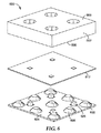
本発明は、複数のLEDを用いる光源に関する。LEDは、規則的なアレイに設けられてもよい。2×2アレイについて以下の説明では記載されるが、本発明は他の数のLEDおよび他のサイズのアレイを包含することを意図としていることは十分に認識されよう。図6は、複数のLED光源600の分解立体図を示す概略図を示す。図7Aおよび図7Bにさらに詳細に示したような反射結合器シート602は、シート602を通過するアパーチャで形成される反射結合器604のアレイを備える。下面606における反射結合器604の入力は、LEDおよび蛍光体パッチの幾何構成に適合して整形されてもよく、上面608における反射結合器604の出力は、光ファイバへの入力に適合して整形されてもよい。反射結合器シート602は、反射結合器が形成されるアパーチャを備えた一個部品として成形されてもよい。次に、アパーチャの側壁に、反射性コーティング、たとえばアルミニウムコーティングを設けて反射結合器604を形成してもよい。
The present invention relates to a light source using a plurality of LEDs. The LEDs may be provided in a regular array. Although described in the following description for a 2 × 2 array, it will be appreciated that the present invention is intended to encompass other numbers of LEDs and other sized arrays. FIG. 6 shows a schematic diagram illustrating an exploded view of a plurality of LED
中間層612を含む中間構成部材が、図8にさらに詳細に示されている。中間層612は、一方の側に複数の蛍光体パッチ614を備える。蛍光体パッチ614は、所望の形状および厚さで中間層612に配置されてもよく、反射結合器シートの反射結合器604のパターンと類似のパターンを形成してもよい。中間層612は、半透過性であってもよく、半透過性でなくてもよい。
The intermediate component including the
蛍光体パッチ614は、異なる方法で構成されてもよい。たとえば、パッチ614は中間層612の面に硬化または設置される結合剤の中に配置される蛍光体粒子を収容してもよい。蛍光体粒子は、上述のように、任意の適切なタイプの蛍光体材料、たとえば無機蛍光体または有機蛍光体から形成されてもよい。適切な結合剤材料としては、ニュージャージー州のノーランド・プロダクツ・インコーポレィテッド(Norland Products Inc.,New Jersey)の「ノア81(NOA81)」などの光透過性光学接着剤などが挙げられる。
The
蛍光体パッチ614は、異なる方法を用いて中間層612の上に配置されてもよい。たとえば、蛍光体パッチ614は、シルクスクリーン法などのスクリーン印刷法を用いて、中間層612の上に印刷されてもよい。中間層612の上に蛍光体パッチ614を配置するために用いてもよい他の手法としては、リソグラフィー法、成形法、噴射法などが挙げられる。リソグラフィー法の一実施例は、フォトリソグラフィー法である。成形法の一例は、パッチの位置に対応する凹部を有する圧盤を設けることである。凹部は蛍光体含有材料で充填され、次に圧盤が中間層の面に対して押圧される。噴射法の実施例は、インクジェット印刷である。蛍光体パッチ614は、必要に応じて、印刷後に中間層612の上で硬化されてもよい。
The
LEDサブアセンブリ622は、その表面に実装されるLED626と電流のやりとりを行う導体を保持するためのフレキシブル回路を用いて形成される基板624を備えうる。たとえば、フレキシブル回路は、関連出願である2003年12月2日に出願された「ILLUMINATION ASSEMBLY」という名称の米国特許出願第10/727,220号明細書および米国特許第5,227,008号明細書にさらに記載されるような回路である。
The
LED626は裸のダイとして設けられてもよく、またはダイは封入されていてもよい。LEDサブアセンブリ622はまた、基板624と中間層612との間にLED626用の空間を設けるために、スタンドオフ628を設けてもよい。スタンドオフは、少なくともLED626と同じ高さであってもよく、LED626より高くてもよい。LED626が上部ワイヤボンドを有する場合には、スタンドオフはLED626の上部にあるワイヤボンド用の余地も提供してもよい。ワイヤボンドは、基板624の上面の導体に接続されてもよい。スタンドオフの異なる形状および構造を用いてもよい。たとえば、スタンドオフ628は、図示されているように先細りであってもよく、または平行な側面であってもよい。スタンドオフ628は、円形断面であってもよく、または異なる形状をとってもよい。また、スタンドオフ628は、示されているものとは異なるパターンで、基板624の上に位置決めされてもよい。あるいは、スタンドオフは、蛍光体パッチ614に対向する側でフィルム612の上に位置決めされてもよい。スタンドオフは、蛍光体パッチおよび/または結合器に対するLEDの横方向の配置を支援するために、対向する面の凹部と嵌合してもよい。
The
複数のLED光源の製造方法は、以下の通りである。一旦、反射結合器シート602が完成して、中間層612に蛍光体パッチ614が設けられると、シート602および中間層612は共に接合される。蛍光体パッチ614は、それぞれの反射結合器604のアパーチャに対して位置合わせを行い、実際にはたとえば図2および図3に示されているように、反射結合器604のアパーチャまで延在してもよい。中間層612および結合器シート602は、任意の適切な技術を用いて接合されてもよい。たとえば、中間層612および結合器シート602は、エポキシを用いて共に接合されてもよい。図9に示された反射結合器シート602および中間層612を備え、接合されたサブアセンブリ902は、比較的剛性であってもよいため、次の組み立てステップにおけるサブアセンブリ902の処理を容易にする。
The manufacturing method of a some LED light source is as follows. Once the
サブアセンブリ902は、次にLEDサブアセンブリ622に接合されてもよい。種々の異なる方法を用いて、これを行うことができる。たとえば、エポキシの領域をスタンドオフ628に塗布し、サブアセンブリをスタンドオフ628の上のエポキシに装着してもよい。別の手法において、エポキシなどの過剰な封入剤をLED626の上に加えてもよい。
Subassembly 902 may then be joined to
異なる技術を用いて、蛍光体パッチ614および反射結合器604に対するLED626の横方向の配置を達成してもよい。1つの手法は、LED626を照射し、結合器シート602を透過する光を監視することである。結合器シート602を透過する光の量が最大となるとき、LED626とサブアセンブリとの間の好ましい配置が達成される。
Different techniques may be used to achieve lateral placement of
図10に概略的に示されているように、シール1004、たとえばエポキシのビードが、組み立てられた光源1002の周囲に設けられ、層612と層622との間の空間に埃、塵などが入らないようにしてもよい。シール1004はまた、層612と層622との間の空間を完全に満たしてもよい。
As schematically shown in FIG. 10, a
組み立てられた光源1002は、青色LEDまたはUV LEDのアレイを用いて指向性の白色光を生成する。光ファイバは、反射結合器シート602にあるそれぞれの開口部に結合されるため、照射用の所望の位置に光を誘導することが可能である。
The assembled
光源1002は、短波長LEDから効率的に向けられる白色または広帯域の光源のコスト効率のよい組み立てを可能にする。複数のLEDを覆う大きなシートにおける中間層の使用により、LED自体に蛍光体材料を直接印刷する複雑な工程を回避し、シートを蛍光体パッチに適合する小さな領域に切断する必要性を回避する。さらに、中間層に反射特性を与えて、波長変換効率を増大させてもよい。また、隣接するLED間の中間層の過剰な材料のコストを低減することから、中間層の添加が光源に用いられる材料のコストを実質的に増大させることにはならない。したがって、中間層は、低コストを維持し、光源の組み立てを簡素化する。さらに、接合ステップおよび配置ステップは、LEDの上部にワイヤボンドなどの関連領域にあまり応力を与えることなく、剛性かつ封入されるアセンブリを生じることになる。
The
本発明は、上述の特定の実施例に限定されるものと考えるべきではなく、添付の特許請求の範囲に完全に記載されているように、本発明のすべての態様を包含するものと考えるべきである。本発明を適用可能であると考えられる種々の変更、等価な方法、ならびに種々の構造は、本願明細書を検討すれば、本発明に関係する当業者には容易に明白となるであろう。特許請求の範囲は、そのような変更および装置を包含することを意図している。 The present invention should not be construed as limited to the particular embodiments described above, but should be construed as encompassing all aspects of the invention as fully set forth in the appended claims. It is. Various modifications, equivalent methods, and various structures that may be applicable to the present invention will be readily apparent to those of skill in the art to which the present invention relates upon review of this specification. The claims are intended to cover such modifications and devices.
Claims (39)
それぞれのLEDダイからの光を結合するための光結合器と、
前記LEDダイと前記光結合器との間に配置され、それぞれのLEDダイから前記光結合器に伝搬する前記LED光の少なくとも一部を変換する蛍光体パッチと、
前記LEDダイと前記蛍光体パッチとの間に配置された中間層であって、前記LED光を透過し、前記蛍光体パッチで変換される光を反射し、前記LEDダイに面する第1の側および前記結合器に面する第2の側を有する中間層と、を含んで成る、前記蛍光体パッチは前記中間層の前記第2の側の上に配置された光源。 A light emitting diode (LED) die capable of emitting LED light;
An optical coupler for combining light from each LED die;
A phosphor patch disposed between the LED die and the optical coupler and converting at least a portion of the LED light propagating from the respective LED die to the optical coupler;
A first intermediate layer disposed between the LED die and the phosphor patch, which transmits the LED light, reflects light converted by the phosphor patch, and faces the LED die; An intermediate layer having a side and a second side facing the coupler, wherein the phosphor patch is disposed on the second side of the intermediate layer.
前記LEDダイからの光を結合するための2つ以上のそれぞれの結合器と、
前記LEDダイと前記結合器との間に配置され、LED光に対して実質的に透明である中間層と、
前記中間層と前記結合器との間で、前記中間層の上に配置され、前記LED光の少なくとも一部を変換波長の光に変換するための蛍光体層と、を含んで成る光源。 Two or more light emitting diode (LED) dies for generating LED light;
Two or more respective couplers for coupling light from the LED die;
An intermediate layer disposed between the LED die and the coupler and substantially transparent to LED light;
A light source comprising a phosphor layer disposed on the intermediate layer and converting at least part of the LED light into light having a conversion wavelength between the intermediate layer and the coupler.
前記LEDダイの上方に配置され、LED光に対して実質的に透明である第1の層であって、前記LED光が前記第1の層の中を前記第1の層の第1の側から前記第1の層の第2の側に伝搬する第1の層と、
前記第1の層の前記第2の側の上に配置された蛍光体層と、を含んで成る光源。 A plurality of light emitting diode (LED) dies capable of emitting LED light;
A first layer disposed above the LED die and substantially transparent to LED light, wherein the LED light passes through the first layer on a first side of the first layer. A first layer propagating from the first layer to the second side of the first layer;
A phosphor layer disposed on the second side of the first layer.
第1の層の上に蛍光体の層を配置するステップであって、前記第1の層はLED光に対して実質的に透明であるステップと、
前記LEDダイの上に前記第1の層および前記蛍光体の層を位置決めし、LED光が前記第1の層の中を前記LEDダイから前記蛍光体の層に向かって通過するようにするステップと、を含む光源の組み立て方法。 Providing a plurality of light emitting diode (LED) dies capable of emitting LED light;
Disposing a layer of phosphor on the first layer, wherein the first layer is substantially transparent to LED light;
Positioning the first layer and the phosphor layer on the LED die and allowing LED light to pass through the first layer from the LED die toward the phosphor layer. And a method of assembling the light source.
Applications Claiming Priority (2)
| Application Number | Priority Date | Filing Date | Title |
|---|---|---|---|
| US10/726,248 US20050116635A1 (en) | 2003-12-02 | 2003-12-02 | Multiple LED source and method for assembling same |
| PCT/US2004/036679 WO2005062098A1 (en) | 2003-12-02 | 2004-11-03 | Light source using a plurality of leds, and method of assembling the same |
Publications (2)
| Publication Number | Publication Date |
|---|---|
| JP2007513381A true JP2007513381A (en) | 2007-05-24 |
| JP2007513381A5 JP2007513381A5 (en) | 2007-12-20 |
Family
ID=34620478
Family Applications (1)
| Application Number | Title | Priority Date | Filing Date |
|---|---|---|---|
| JP2006542584A Withdrawn JP2007513381A (en) | 2003-12-02 | 2004-11-03 | Light source using a plurality of LEDs and method of assembling the light source |
Country Status (7)
| Country | Link |
|---|---|
| US (1) | US20050116635A1 (en) |
| EP (1) | EP1690120A1 (en) |
| JP (1) | JP2007513381A (en) |
| KR (1) | KR20060113981A (en) |
| CN (1) | CN1902519A (en) |
| TW (1) | TW200529472A (en) |
| WO (1) | WO2005062098A1 (en) |
Cited By (3)
| Publication number | Priority date | Publication date | Assignee | Title |
|---|---|---|---|---|
| JP2009224277A (en) * | 2008-03-18 | 2009-10-01 | Yamaguchi Univ | Indoor lighting device |
| JP2010537249A (en) * | 2007-08-21 | 2010-12-02 | ワイエルエックス,リミテッド | Optical coupler for light emitting devices with enhanced output brightness |
| JP2011048371A (en) * | 2009-08-28 | 2011-03-10 | General Electric Co <Ge> | Apparatus for coupling between light emitting diode and light guide |
Families Citing this family (56)
| Publication number | Priority date | Publication date | Assignee | Title |
|---|---|---|---|---|
| CN100383573C (en) * | 2002-12-02 | 2008-04-23 | 3M创新有限公司 | Illumination system using a plurality of light sources |
| WO2004068603A2 (en) * | 2003-01-27 | 2004-08-12 | 3M Innovative Properties Company | Phosphor based light source component and method of making |
| US7520635B2 (en) * | 2003-07-02 | 2009-04-21 | S.C. Johnson & Son, Inc. | Structures for color changing light devices |
| EP2803898B1 (en) * | 2004-05-05 | 2020-08-19 | Rensselaer Polytechnic Institute | A light-emitting apparatus |
| US7837348B2 (en) * | 2004-05-05 | 2010-11-23 | Rensselaer Polytechnic Institute | Lighting system using multiple colored light emitting sources and diffuser element |
| US7204630B2 (en) * | 2004-06-30 | 2007-04-17 | 3M Innovative Properties Company | Phosphor based illumination system having a plurality of light guides and an interference reflector |
| US7204631B2 (en) * | 2004-06-30 | 2007-04-17 | 3M Innovative Properties Company | Phosphor based illumination system having a plurality of light guides and an interference reflector |
| US7182498B2 (en) * | 2004-06-30 | 2007-02-27 | 3M Innovative Properties Company | Phosphor based illumination system having a plurality of light guides and an interference reflector |
| US7255469B2 (en) * | 2004-06-30 | 2007-08-14 | 3M Innovative Properties Company | Phosphor based illumination system having a light guide and an interference reflector |
| US7213958B2 (en) * | 2004-06-30 | 2007-05-08 | 3M Innovative Properties Company | Phosphor based illumination system having light guide and an interference reflector |
| CN101014295A (en) * | 2004-07-02 | 2007-08-08 | 底斯柯斯牙齿印模公司 | Curing light device having a reflector |
| KR100668609B1 (en) * | 2004-09-24 | 2007-01-16 | 엘지전자 주식회사 | Device of White Light Source |
| KR101266130B1 (en) * | 2005-06-23 | 2013-05-27 | 렌슬러 폴리테크닉 인스티튜트 | Package design for producing white light with short-wavelength leds and down-conversion materials |
| EP1902247A2 (en) * | 2005-07-12 | 2008-03-26 | Magna International Inc | Semiconductor light engine for automotive lighting |
| US7560742B2 (en) * | 2005-11-28 | 2009-07-14 | Magna International Inc. | Semiconductor-based lighting systems and lighting system components for automotive use |
| US20090008655A1 (en) * | 2006-01-31 | 2009-01-08 | Koninklijke Philips Electronics N.V. | White Light Source |
| US7846391B2 (en) | 2006-05-22 | 2010-12-07 | Lumencor, Inc. | Bioanalytical instrumentation using a light source subsystem |
| US7703942B2 (en) * | 2006-08-31 | 2010-04-27 | Rensselaer Polytechnic Institute | High-efficient light engines using light emitting diodes |
| US7889421B2 (en) | 2006-11-17 | 2011-02-15 | Rensselaer Polytechnic Institute | High-power white LEDs and manufacturing method thereof |
| CN101680804B (en) * | 2007-04-03 | 2012-01-11 | 武藤工业株式会社 | Spectrophotometer and method |
| US7709811B2 (en) * | 2007-07-03 | 2010-05-04 | Conner Arlie R | Light emitting diode illumination system |
| TW200903851A (en) * | 2007-07-10 | 2009-01-16 | Univ Nat Central | Phosphor package of light emitting diodes |
| KR101134996B1 (en) * | 2007-07-26 | 2012-04-09 | 파나소닉 주식회사 | Led lighting device |
| US7547114B2 (en) | 2007-07-30 | 2009-06-16 | Ylx Corp. | Multicolor illumination device using moving plate with wavelength conversion materials |
| US8098375B2 (en) | 2007-08-06 | 2012-01-17 | Lumencor, Inc. | Light emitting diode illumination system |
| US7863635B2 (en) | 2007-08-07 | 2011-01-04 | Cree, Inc. | Semiconductor light emitting devices with applied wavelength conversion materials |
| DE102008012316B4 (en) * | 2007-09-28 | 2023-02-02 | OSRAM Opto Semiconductors Gesellschaft mit beschränkter Haftung | Semiconductor light source with a primary radiation source and a luminescence conversion element |
| US20090108269A1 (en) * | 2007-10-26 | 2009-04-30 | Led Lighting Fixtures, Inc. | Illumination device having one or more lumiphors, and methods of fabricating same |
| WO2009117834A1 (en) | 2008-03-26 | 2009-10-01 | Magna International Inc. | Fog lamp and the like employing semiconductor light sources |
| CA2664963A1 (en) * | 2008-05-01 | 2009-11-01 | Magna International Inc. | Hotspot cutoff d-optic |
| EP2332128A4 (en) * | 2008-07-18 | 2014-02-19 | Isaac S Daniel | System and method for countering terrorsm by monitoring containers over international seas |
| US20100127299A1 (en) * | 2008-11-25 | 2010-05-27 | Cooper Technologies Company | Actively Cooled LED Lighting System and Method for Making the Same |
| US8242462B2 (en) | 2009-01-23 | 2012-08-14 | Lumencor, Inc. | Lighting design of high quality biomedical devices |
| US8921876B2 (en) | 2009-06-02 | 2014-12-30 | Cree, Inc. | Lighting devices with discrete lumiphor-bearing regions within or on a surface of remote elements |
| KR20120090064A (en) * | 2009-09-15 | 2012-08-16 | 쓰리엠 이노베이티브 프로퍼티즈 컴파니 | Led projector and method |
| JP2014503117A (en) * | 2010-12-29 | 2014-02-06 | スリーエム イノベイティブ プロパティズ カンパニー | Remote phosphor LED device with broadband output and controllable color |
| US8912562B2 (en) | 2010-12-29 | 2014-12-16 | 3M Innovative Properties Company | Remote phosphor LED constructions |
| US8389957B2 (en) | 2011-01-14 | 2013-03-05 | Lumencor, Inc. | System and method for metered dosage illumination in a bioanalysis or other system |
| US8466436B2 (en) | 2011-01-14 | 2013-06-18 | Lumencor, Inc. | System and method for metered dosage illumination in a bioanalysis or other system |
| US8967846B2 (en) | 2012-01-20 | 2015-03-03 | Lumencor, Inc. | Solid state continuous white light source |
| US20130279149A1 (en) * | 2012-04-19 | 2013-10-24 | Sumitronics Taiwan Co., Ltd. | Led light bulb |
| US9217561B2 (en) | 2012-06-15 | 2015-12-22 | Lumencor, Inc. | Solid state light source for photocuring |
| JP6140730B2 (en) * | 2012-12-10 | 2017-05-31 | 株式会社エルム | Method for creating phosphor layer |
| US10788678B2 (en) | 2013-05-17 | 2020-09-29 | Excelitas Canada, Inc. | High brightness solid state illumination system for fluorescence imaging and analysis |
| US9158080B2 (en) * | 2013-08-23 | 2015-10-13 | Corning Incorporated | Light-coupling apparatus and methods for light-diffusing optical fibers |
| CN110890449B (en) * | 2014-01-09 | 2023-11-07 | 亮锐控股有限公司 | Light emitting device with reflective sidewalls |
| JP6680868B2 (en) | 2015-08-17 | 2020-04-15 | インフィニット アースロスコピー インコーポレーテッド, リミテッド | light source |
| WO2017087448A1 (en) | 2015-11-16 | 2017-05-26 | Infinite Arthroscopy Inc, Limited | Wireless medical imaging system |
| US20180114870A1 (en) * | 2016-10-23 | 2018-04-26 | Nanya Technology Corporation | Optical package structure |
| CA3053471C (en) | 2017-02-15 | 2022-05-10 | Infinite Arthroscopy, Inc. Limited | Wireless medical imaging system comprising a head unit and a light cable that comprises an integrated light source |
| CN109656085B (en) * | 2017-10-10 | 2020-12-01 | 深圳市绎立锐光科技开发有限公司 | Light emitting device and automobile lighting device using same |
| US11063245B2 (en) | 2018-12-14 | 2021-07-13 | Lg Display Co., Ltd. | Display apparatus |
| US11342311B2 (en) * | 2019-03-18 | 2022-05-24 | Intematix Corporation | LED-filaments and LED-filament lamps utilizing manganese-activated fluoride red photoluminescence material |
| TR202006149A2 (en) * | 2020-03-11 | 2020-12-21 | Rd Global Arastirma Gelistirme Saglik Ilac Insaat Yatirimlari Sanayi Ve Ticaret Anonim Sirketi | ULTRAVIOLE AND LASER (RED BEAM, GREEN BEAM) RAY TREATMENT |
| USD938584S1 (en) | 2020-03-30 | 2021-12-14 | Lazurite Holdings Llc | Hand piece |
| USD972176S1 (en) | 2020-08-06 | 2022-12-06 | Lazurite Holdings Llc | Light source |
Family Cites Families (98)
| Publication number | Priority date | Publication date | Assignee | Title |
|---|---|---|---|---|
| US692190A (en) * | 1901-09-03 | 1902-01-28 | J H Thies | Disk plow. |
| US3825335A (en) * | 1973-01-04 | 1974-07-23 | Polaroid Corp | Variable color photographic lighting system |
| US3902059A (en) * | 1974-02-15 | 1975-08-26 | Esquire Inc | Light reflector system |
| US4254453A (en) * | 1978-08-25 | 1981-03-03 | General Instrument Corporation | Alpha-numeric display array and method of manufacture |
| DE3069386D1 (en) * | 1979-12-22 | 1984-11-08 | Lucas Ind Plc | Motor vehicle lamp reflector |
| JPS6019564A (en) * | 1983-07-13 | 1985-01-31 | Fuji Photo Film Co Ltd | Side printer |
| US4755918A (en) * | 1987-04-06 | 1988-07-05 | Lumitex, Inc. | Reflector system |
| US4914731A (en) * | 1987-08-12 | 1990-04-03 | Chen Shen Yuan | Quickly formed light emitting diode display and a method for forming the same |
| US4897771A (en) * | 1987-11-24 | 1990-01-30 | Lumitex, Inc. | Reflector and light system |
| US5146248A (en) * | 1987-12-23 | 1992-09-08 | North American Philips Corporation | Light valve projection system with improved illumination |
| US5140248A (en) * | 1987-12-23 | 1992-08-18 | Allen-Bradley Company, Inc. | Open loop motor control with both voltage and current regulation |
| US4964025A (en) * | 1988-10-05 | 1990-10-16 | Hewlett-Packard Company | Nonimaging light source |
| US5155336A (en) * | 1990-01-19 | 1992-10-13 | Applied Materials, Inc. | Rapid thermal heating apparatus and method |
| US5227008A (en) * | 1992-01-23 | 1993-07-13 | Minnesota Mining And Manufacturing Company | Method for making flexible circuits |
| DE4301716C2 (en) * | 1992-02-04 | 1999-08-12 | Hitachi Ltd | Projection exposure device and method |
| US5299222A (en) * | 1992-03-11 | 1994-03-29 | Lightwave Electronics | Multiple diode laser stack for pumping a solid-state laser |
| US5301090A (en) * | 1992-03-16 | 1994-04-05 | Aharon Z. Hed | Luminaire |
| US5337325A (en) * | 1992-05-04 | 1994-08-09 | Photon Imaging Corp | Semiconductor, light-emitting devices |
| US5293437A (en) * | 1992-06-03 | 1994-03-08 | Visual Optics, Inc. | Fiber optic display with direct driven optical fibers |
| US5317484A (en) * | 1993-02-01 | 1994-05-31 | General Electric Company | Collection optics for high brightness discharge light source |
| US5810469A (en) * | 1993-03-26 | 1998-09-22 | Weinreich; Steve | Combination light concentrating and collimating device and light fixture and display screen employing the same |
| US5534718A (en) * | 1993-04-12 | 1996-07-09 | Hsi-Huang Lin | LED package structure of LED display |
| US5420768A (en) * | 1993-09-13 | 1995-05-30 | Kennedy; John | Portable led photocuring device |
| DE4341234C2 (en) * | 1993-12-03 | 2002-09-12 | Bosch Gmbh Robert | Lighting device for vehicles |
| US5882774A (en) * | 1993-12-21 | 1999-03-16 | Minnesota Mining And Manufacturing Company | Optical film |
| DE4429913C1 (en) * | 1994-08-23 | 1996-03-21 | Fraunhofer Ges Forschung | Device and method for plating |
| DE4430778C2 (en) * | 1994-08-30 | 2000-01-27 | Sick Ag | Tube |
| US5713654A (en) * | 1994-09-28 | 1998-02-03 | Sdl, Inc. | Addressable laser vehicle lights |
| US5611017A (en) * | 1995-06-01 | 1997-03-11 | Minnesota Mining And Manufacturing Co. | Fiber optic ribbon cable with pre-installed locations for subsequent connectorization |
| US5629996A (en) * | 1995-11-29 | 1997-05-13 | Physical Optics Corporation | Universal remote lighting system with nonimaging total internal reflection beam transformer |
| US6239868B1 (en) * | 1996-01-02 | 2001-05-29 | Lj Laboratories, L.L.C. | Apparatus and method for measuring optical characteristics of an object |
| US5661839A (en) * | 1996-03-22 | 1997-08-26 | The University Of British Columbia | Light guide employing multilayer optical film |
| US6045240A (en) * | 1996-06-27 | 2000-04-04 | Relume Corporation | LED lamp assembly with means to conduct heat away from the LEDS |
| US5816694A (en) * | 1996-06-28 | 1998-10-06 | General Electric Company | Square distribution reflector |
| FI103074B (en) * | 1996-07-17 | 1999-04-15 | Valtion Teknillinen | spectrometer |
| US6608332B2 (en) * | 1996-07-29 | 2003-08-19 | Nichia Kagaku Kogyo Kabushiki Kaisha | Light emitting device and display |
| US5808794A (en) * | 1996-07-31 | 1998-09-15 | Weber; Michael F. | Reflective polarizers having extended red band edge for controlled off axis color |
| US5709463A (en) * | 1996-08-13 | 1998-01-20 | Delco Electronics Corporation | Backlighting for bright liquid crystal display |
| US5727108A (en) * | 1996-09-30 | 1998-03-10 | Troy Investments, Inc. | High efficiency compound parabolic concentrators and optical fiber powered spot luminaire |
| US6104446A (en) * | 1996-12-18 | 2000-08-15 | Blankenbecler; Richard | Color separation optical plate for use with LCD panels |
| US6587573B1 (en) * | 2000-03-20 | 2003-07-01 | Gentex Corporation | System for controlling exterior vehicle lights |
| JPH10319871A (en) * | 1997-05-19 | 1998-12-04 | Kouha:Kk | Led display device |
| US6952504B2 (en) * | 2001-12-21 | 2005-10-04 | Neophotonics Corporation | Three dimensional engineering of planar optical structures |
| US5967653A (en) * | 1997-08-06 | 1999-10-19 | Miller; Jack V. | Light projector with parabolic transition format coupler |
| US6340824B1 (en) * | 1997-09-01 | 2002-01-22 | Kabushiki Kaisha Toshiba | Semiconductor light emitting device including a fluorescent material |
| US5909037A (en) * | 1998-01-12 | 1999-06-01 | Hewlett-Packard Company | Bi-level injection molded leadframe |
| US6200134B1 (en) * | 1998-01-20 | 2001-03-13 | Kerr Corporation | Apparatus and method for curing materials with radiation |
| DE69916344T2 (en) * | 1998-01-23 | 2005-05-12 | Océ-Technologies B.V. | Pizoelectric actuator for inkjet printhead |
| US6290382B1 (en) * | 1998-08-17 | 2001-09-18 | Ppt Vision, Inc. | Fiber bundle combiner and led illumination system and method |
| US5959316A (en) * | 1998-09-01 | 1999-09-28 | Hewlett-Packard Company | Multiple encapsulation of phosphor-LED devices |
| WO2000036336A1 (en) * | 1998-12-17 | 2000-06-22 | Koninklijke Philips Electronics N.V. | Light engine |
| US6414801B1 (en) * | 1999-01-14 | 2002-07-02 | Truck-Lite Co., Inc. | Catadioptric light emitting diode assembly |
| EP1031326A1 (en) * | 1999-02-05 | 2000-08-30 | Jean-Michel Decaudin | Device for photo-activation of photosensitive composite materials especially in dentistry |
| US6172810B1 (en) * | 1999-02-26 | 2001-01-09 | 3M Innovative Properties Company | Retroreflective articles having polymer multilayer reflective coatings |
| US6556734B1 (en) * | 1999-04-19 | 2003-04-29 | Gemfire Corporation | Electrical connection scheme for optical devices |
| US6193392B1 (en) * | 1999-05-27 | 2001-02-27 | Pervaiz Lodhie | Led array with a multi-directional, multi-functional light reflector |
| TW493054B (en) * | 1999-06-25 | 2002-07-01 | Koninkl Philips Electronics Nv | Vehicle headlamp and a vehicle |
| US6504301B1 (en) * | 1999-09-03 | 2003-01-07 | Lumileds Lighting, U.S., Llc | Non-incandescent lightbulb package using light emitting diodes |
| JP4517271B2 (en) * | 1999-09-10 | 2010-08-04 | 株式会社ニコン | Exposure apparatus equipped with a laser device |
| DE69910390T2 (en) * | 1999-10-15 | 2004-07-22 | Automotive Lighting Italia S.P.A., Venaria Reale | Lighting device for motor vehicles with a strongly discontinuous reflector surface |
| US6784982B1 (en) * | 1999-11-04 | 2004-08-31 | Regents Of The University Of Minnesota | Direct mapping of DNA chips to detector arrays |
| US6350041B1 (en) * | 1999-12-03 | 2002-02-26 | Cree Lighting Company | High output radial dispersing lamp using a solid state light source |
| DE10006738C2 (en) * | 2000-02-15 | 2002-01-17 | Osram Opto Semiconductors Gmbh | Light-emitting component with improved light decoupling and method for its production |
| US6625351B2 (en) * | 2000-02-17 | 2003-09-23 | Microfab Technologies, Inc. | Ink-jet printing of collimating microlenses onto optical fibers |
| US6224216B1 (en) * | 2000-02-18 | 2001-05-01 | Infocus Corporation | System and method employing LED light sources for a projection display |
| JP4406490B2 (en) * | 2000-03-14 | 2010-01-27 | 株式会社朝日ラバー | Light emitting diode |
| US6603258B1 (en) * | 2000-04-24 | 2003-08-05 | Lumileds Lighting, U.S. Llc | Light emitting diode device that emits white light |
| US6570186B1 (en) * | 2000-05-10 | 2003-05-27 | Toyoda Gosei Co., Ltd. | Light emitting device using group III nitride compound semiconductor |
| DE10033502A1 (en) * | 2000-07-10 | 2002-01-31 | Osram Opto Semiconductors Gmbh | Optoelectronic module, process for its production and its use |
| US6527411B1 (en) * | 2000-08-01 | 2003-03-04 | Visteon Corporation | Collimating lamp |
| US6614103B1 (en) * | 2000-09-01 | 2003-09-02 | General Electric Company | Plastic packaging of LED arrays |
| DE10051159C2 (en) * | 2000-10-16 | 2002-09-19 | Osram Opto Semiconductors Gmbh | LED module, e.g. White light source |
| AT410266B (en) * | 2000-12-28 | 2003-03-25 | Tridonic Optoelectronics Gmbh | LIGHT SOURCE WITH A LIGHT-EMITTING ELEMENT |
| DE10065624C2 (en) * | 2000-12-29 | 2002-11-14 | Hans Kragl | Coupling arrangement for optically coupling an optical waveguide to an electro-optical or opto-electrical semiconductor converter |
| TW490863B (en) * | 2001-02-12 | 2002-06-11 | Arima Optoelectronics Corp | Manufacturing method of LED with uniform color temperature |
| US6541800B2 (en) * | 2001-02-22 | 2003-04-01 | Weldon Technologies, Inc. | High power LED |
| US20020126479A1 (en) * | 2001-03-08 | 2002-09-12 | Ball Semiconductor, Inc. | High power incoherent light source with laser array |
| CN1212676C (en) * | 2001-04-12 | 2005-07-27 | 松下电工株式会社 | Light source device using LED, and method of producing same |
| JP3962219B2 (en) * | 2001-04-26 | 2007-08-22 | 貴志 山田 | Phototherapy device using polarized light |
| DE10127542C2 (en) * | 2001-05-31 | 2003-06-18 | Infineon Technologies Ag | Coupling arrangement for optically coupling a light guide to a light receiver |
| US6777870B2 (en) * | 2001-06-29 | 2004-08-17 | Intel Corporation | Array of thermally conductive elements in an oled display |
| EP1416219B1 (en) * | 2001-08-09 | 2016-06-22 | Everlight Electronics Co., Ltd | Led illuminator and card type led illuminating light source |
| US6921920B2 (en) * | 2001-08-31 | 2005-07-26 | Smith & Nephew, Inc. | Solid-state light source |
| US20030068113A1 (en) * | 2001-09-12 | 2003-04-10 | Siegfried Janz | Method for polarization birefringence compensation in a waveguide demultiplexer using a compensator with a high refractive index capping layer. |
| JP4067801B2 (en) * | 2001-09-18 | 2008-03-26 | 松下電器産業株式会社 | Lighting device |
| US20030057421A1 (en) * | 2001-09-27 | 2003-03-27 | Tzer-Perng Chen | High flux light emitting diode having flip-chip type light emitting diode chip with a transparent substrate |
| US7144248B2 (en) * | 2001-10-18 | 2006-12-05 | Irwin Dean S | Device for oral UV photo-therapy |
| US20030091277A1 (en) * | 2001-11-15 | 2003-05-15 | Wenhui Mei | Flattened laser scanning system |
| US6560038B1 (en) * | 2001-12-10 | 2003-05-06 | Teledyne Lighting And Display Products, Inc. | Light extraction from LEDs with light pipes |
| US6928226B2 (en) * | 2002-03-14 | 2005-08-09 | Corning Incorporated | Fiber and lens grippers, optical devices and methods of manufacture |
| US7095922B2 (en) * | 2002-03-26 | 2006-08-22 | Ngk Insulators, Ltd. | Lensed fiber array and production method thereof |
| JP3707688B2 (en) * | 2002-05-31 | 2005-10-19 | スタンレー電気株式会社 | Light emitting device and manufacturing method thereof |
| US7029277B2 (en) * | 2002-10-17 | 2006-04-18 | Coltene / Whaledent Inc. | Curing light with engineered spectrum and power compressor guide |
| US20040164325A1 (en) * | 2003-01-09 | 2004-08-26 | Con-Trol-Cure, Inc. | UV curing for ink jet printer |
| US7211299B2 (en) * | 2003-01-09 | 2007-05-01 | Con-Trol-Cure, Inc. | UV curing method and apparatus |
| US20040159900A1 (en) * | 2003-01-27 | 2004-08-19 | 3M Innovative Properties Company | Phosphor based light sources having front illumination |
| US6950454B2 (en) * | 2003-03-24 | 2005-09-27 | Eastman Kodak Company | Electronic imaging system using organic laser array illuminating an area light valve |
| US7300164B2 (en) * | 2004-08-26 | 2007-11-27 | Hewlett-Packard Development Company, L.P. | Morphing light guide |
-
2003
- 2003-12-02 US US10/726,248 patent/US20050116635A1/en not_active Abandoned
-
2004
- 2004-11-03 JP JP2006542584A patent/JP2007513381A/en not_active Withdrawn
- 2004-11-03 EP EP04820738A patent/EP1690120A1/en not_active Withdrawn
- 2004-11-03 CN CNA2004800392905A patent/CN1902519A/en active Pending
- 2004-11-03 KR KR1020067013168A patent/KR20060113981A/en not_active Application Discontinuation
- 2004-11-03 WO PCT/US2004/036679 patent/WO2005062098A1/en not_active Application Discontinuation
- 2004-11-18 TW TW093135483A patent/TW200529472A/en unknown
Cited By (3)
| Publication number | Priority date | Publication date | Assignee | Title |
|---|---|---|---|---|
| JP2010537249A (en) * | 2007-08-21 | 2010-12-02 | ワイエルエックス,リミテッド | Optical coupler for light emitting devices with enhanced output brightness |
| JP2009224277A (en) * | 2008-03-18 | 2009-10-01 | Yamaguchi Univ | Indoor lighting device |
| JP2011048371A (en) * | 2009-08-28 | 2011-03-10 | General Electric Co <Ge> | Apparatus for coupling between light emitting diode and light guide |
Also Published As
| Publication number | Publication date |
|---|---|
| KR20060113981A (en) | 2006-11-03 |
| WO2005062098A1 (en) | 2005-07-07 |
| TW200529472A (en) | 2005-09-01 |
| EP1690120A1 (en) | 2006-08-16 |
| CN1902519A (en) | 2007-01-24 |
| US20050116635A1 (en) | 2005-06-02 |
Similar Documents
| Publication | Publication Date | Title |
|---|---|---|
| JP2007513381A (en) | Light source using a plurality of LEDs and method of assembling the light source | |
| TWI390266B (en) | Illumination system,vehicle headlight,projection system,light fixture,sign,display and method of providing illumination | |
| US7329887B2 (en) | Solid state light device | |
| KR101318582B1 (en) | Phosphor based illumination system having a long pass reflector and method of making same | |
| US7213958B2 (en) | Phosphor based illumination system having light guide and an interference reflector | |
| US7204631B2 (en) | Phosphor based illumination system having a plurality of light guides and an interference reflector | |
| US7163327B2 (en) | Illumination system using a plurality of light sources | |
| US7182498B2 (en) | Phosphor based illumination system having a plurality of light guides and an interference reflector | |
| US20060002108A1 (en) | Phosphor based illumination system having a short pass reflector and method of making same | |
| US20080225549A1 (en) | Linear Optic Light Coupler | |
| WO2006007388A1 (en) | Solid state light device | |
| WO2012006123A2 (en) | Optical beam shaping and polarization selection on led with wavelength conversion | |
| JP2011501427A (en) | Side-emitting LED light source for backlighting applications | |
| CN110799877B (en) | High brightness light conversion device | |
| KR102127968B1 (en) | lighting device |
Legal Events
| Date | Code | Title | Description |
|---|---|---|---|
| A521 | Written amendment |
Free format text: JAPANESE INTERMEDIATE CODE: A523 Effective date: 20071101 |
|
| A621 | Written request for application examination |
Free format text: JAPANESE INTERMEDIATE CODE: A621 Effective date: 20071101 |
|
| A761 | Written withdrawal of application |
Free format text: JAPANESE INTERMEDIATE CODE: A761 Effective date: 20080519 |