JP2007334076A - Optical diffraction structure - Google Patents
Optical diffraction structure Download PDFInfo
- Publication number
- JP2007334076A JP2007334076A JP2006166884A JP2006166884A JP2007334076A JP 2007334076 A JP2007334076 A JP 2007334076A JP 2006166884 A JP2006166884 A JP 2006166884A JP 2006166884 A JP2006166884 A JP 2006166884A JP 2007334076 A JP2007334076 A JP 2007334076A
- Authority
- JP
- Japan
- Prior art keywords
- grating
- diffraction
- pitch
- continuously
- angle
- Prior art date
- Legal status (The legal status is an assumption and is not a legal conclusion. Google has not performed a legal analysis and makes no representation as to the accuracy of the status listed.)
- Pending
Links
Images


Abstract
Description
本発明は、光回折構造に関し、詳しくは、回折格子によってグラデーション効果を表現する手法において、回折格子の格子ピッチと格子角度を同時に、かつ、連続的に変化させた光回折構造に関する。 The present invention relates to an optical diffractive structure, and more particularly to an optical diffractive structure in which a grating pitch and a grating angle of a diffraction grating are changed simultaneously and continuously in a technique for expressing a gradation effect by a diffraction grating.
ホログラムや回折格子などは、特殊な装飾像や立体像を表現できることから、意匠性を高めた印刷物等に利用されている。また、製造のために高度な技術を要することから、偽造防止手段として利用されている。
意匠性を高めるために使用される分野としては、高額な商品の包装材,パンフレット,POP,書籍の表紙等で、偽造防止手段として使用される分野としては、例えば、クレジットカード,IDカード等のカード類や、商品券,小切手,手形,株券,入場券等の金券類,各種証明書等である。
また、これら、ホログラムや回折格子などを対象物に貼付する方法として、熱転写によって貼付する方法や、ラベルにして貼付する方法がある。
熱転写による方法は、長期間使用され、平坦な貼付面を有する前述のカード類,金券類に多く利用され、ラベルによる方法は、貼付される対象物が平坦な面を持たない場合等に利用される。
Holograms, diffraction gratings, and the like can express special decorative images and three-dimensional images, and are therefore used for printed materials with improved design. Further, since advanced technology is required for production, it is used as a means for preventing forgery.
Fields used to enhance design properties include high-priced product packaging materials, pamphlets, POPs, book covers, etc., and fields used as anti-counterfeiting means include, for example, credit cards, ID cards, etc. Cards, gift vouchers such as gift certificates, checks, bills, stock certificates, admission tickets, and various certificates.
In addition, as a method of attaching these holograms and diffraction gratings to an object, there are a method of attaching by thermal transfer and a method of attaching as a label.
The thermal transfer method is used for a long time and is often used for the aforementioned cards and cash vouchers that have a flat application surface. The label method is used when the object to be applied does not have a flat surface. The
前述の意匠性を高めるために使用される回折格子として、「回折格子パターンを有するディスプレイ」が提供されている(例えば、特許文献1参照)。
特許文献1に紹介されている技術は、平面状の基板の表面に、微小な回折格子(グレーティング)からなるセルを複数個配設することにより形成されるディスプレイにおいて、ディスプレイ本体を作製するための第一の元データに基づいて、各回折格子セルを構成する回折格子の線幅と格子間隔との比を適切に変化させることにより再生時の各回折格子のセルの回折光強度を抑制するものであるとしている。
A “display having a diffraction grating pattern” has been provided as a diffraction grating used to enhance the above-described designability (see, for example, Patent Document 1).
The technique introduced in
特許文献1に開示されている技術は、電子線露光装置等の二値デバイスを用いても階調表現が簡便に実現でき、また、複製工程においても成形性がよく、より簡便な複製を行うことが可能な回折格子パターンを有するディスプレイを提供することが目的であるとしており、三次元的に階調を表現する光回折構造を提供するものではない。
そこで本発明は、回折格子の格子ピッチと格子角度を同時に、かつ、連続的に変化させ、三次元的に階調を表現する光回折構造を提供することを目的とする。
The technique disclosed in
SUMMARY OF THE INVENTION An object of the present invention is to provide an optical diffraction structure in which a grating pitch and a grating angle of a diffraction grating are changed simultaneously and continuously to express a gradation in three dimensions.
前記課題を解決するために、本発明の光回折構造の第一の態様は、回折格子の集合により形成された光回折構造であって、回折格子の集合の少なくとも一部に、回折格子の格子ピッチと格子角度が同時に、かつ、連続的に変化する領域を有することを特徴とするものである。 In order to solve the above problems, a first aspect of the light diffraction structure of the present invention is a light diffraction structure formed by a set of diffraction gratings, wherein at least a part of the diffraction grating set includes It has a region where the pitch and the lattice angle change simultaneously and continuously.
また、第二の態様は、第一の態様において、回折格子の格子ピッチと格子角度が同時に、かつ、連続的に変化する領域において、回折格子の格子角度が連続的に変化する方向が円周方向に定義され、回折格子の格子ピッチが連続的に変化する方向がその法線方向で定義されたことを特徴とするものである。 Further, the second aspect is the same as the first aspect, in which the grating angle of the diffraction grating continuously changes in a region where the grating pitch and the grating angle change simultaneously and continuously. The direction in which the grating pitch of the diffraction grating continuously changes is defined as the normal direction.
また、第三の態様は、第一,第二何れかの態様において、回折格子の格子ピッチが0.4〜5.0μmの範囲であることを特徴とするものである。 The third aspect is characterized in that, in any one of the first and second aspects, the grating pitch of the diffraction grating is in the range of 0.4 to 5.0 μm.
1)本発明の光回折構造の第一の態様のように、回折格子の集合により形成された光回折構造であって、回折格子の集合の少なくとも一部に、回折格子の格子ピッチと格子角度が同時に、かつ、連続的に変化する領域を有することによって、その領域は格子ピッチの変化する方向と、格子角度が変化する方向の、質感を持った三次元図柄が得られ、従来にないグラデーション効果を得ることができる。
2)また、第二の態様のように、第一の態様において、回折格子の格子ピッチと格子角度が共に、連続的に変化する領域において、回折格子の格子角度が連続的に変化する方向が円周方向に定義され、回折格子の格子ピッチが連続的に変化する方向がその法線方向で定義されたことによって、その扇形領域内は円周方向にも、中心方向にもグラデーション効果が発生し、あたかも円の中心に向かって光が流れ込んでゆくかのような視認性を有する光回折構造を得ることができる。
3)また、第三の態様のように、第一,第二何れかの態様において、回折格子の格子ピッチが0.4〜5.0μmの範囲であることによって、回折格子ピッチを2.0μm以上とした領域は、回折する割合が減り、あたかも光を吸収しているように見え、例えば、第二の態様において回折格子のピッチを連続的に変化させる際に2.0μm以上のピッチを使用すれば、あたかも2.0μm以上の格子ピッチの領域に向かって光が吸い込まれていくかのような光回折構造を得ることができる。
1) An optical diffractive structure formed by a set of diffraction gratings as in the first aspect of the optical diffractive structure of the present invention, wherein at least part of the set of diffraction gratings includes a grating pitch and a grating angle of the diffraction grating. By having an area that changes at the same time and continuously, the area can produce a three-dimensional design with texture in the direction in which the lattice pitch changes and the direction in which the lattice angle changes, and an unprecedented gradation An effect can be obtained.
2) Also, as in the second aspect, in the first aspect, in the region where both the grating pitch and the grating angle of the diffraction grating continuously change, the direction in which the grating angle of the diffraction grating continuously changes is By defining the normal direction as the direction in which the grating pitch of the diffraction grating continuously changes is defined in the circumferential direction, a gradation effect is generated both in the circumferential direction and in the central direction in the sector area. In addition, it is possible to obtain a light diffraction structure having visibility as if light flows toward the center of the circle.
3) Further, as in the third aspect, in either of the first and second aspects, the diffraction grating pitch is set to 2.0 μm when the grating pitch of the diffraction grating is in the range of 0.4 to 5.0 μm. The above-described region has a reduced ratio of diffraction and appears to absorb light. For example, when the pitch of the diffraction grating is continuously changed in the second mode, a pitch of 2.0 μm or more is used. By doing so, it is possible to obtain an optical diffraction structure as if light is sucked toward a region having a grating pitch of 2.0 μm or more.
以下、図面を参照して、本発明の光回折構造について説明する。
図1は、本発明の光回折構造について説明するための図,図2は、格子ピッチを連続的に変化させた場合の階調について説明するための図,図3は、格子角度を連続的に変化させた場合の階調について説明するための図,図4は、従来の光回折構造の一例について説明するための図,図5は、本発明の光回折構造の一例について説明するための図,である。
Hereinafter, the optical diffraction structure of the present invention will be described with reference to the drawings.
FIG. 1 is a diagram for explaining the optical diffraction structure of the present invention, FIG. 2 is a diagram for explaining gradations when the grating pitch is continuously changed, and FIG. 3 is a diagram showing grating angles continuously. FIG. 4 is a diagram for explaining an example of a conventional light diffraction structure, and FIG. 5 is a diagram for explaining an example of the light diffraction structure of the present invention. Fig.
ホログラムには、物体光と参照光との光の干渉による干渉縞で表現された三次元画像のレリーフホログラムや、二次元画像による回折格子が多く使用される。
意匠性を高める手段として、また、偽造防止手段として、白色光再生ホログラムであるレインボーホログラム,カラーホログラム,さらに、これらのホログラムに文字,図形,記号等を結合させて作製される合成ホログラム等が多く使用される。
As the hologram, a relief hologram of a three-dimensional image expressed by interference fringes due to interference of light between the object light and the reference light, and a diffraction grating based on a two-dimensional image are often used.
As a means for improving design and as a means for preventing forgery, there are many rainbow holograms and color holograms that are white light reproduction holograms, and synthetic holograms produced by combining these holograms with characters, figures, symbols, etc. used.
ホログラムの使用形態として、基材上に転写された状態で使用される場合と、基材上に形成された状態でラベル化して使用される場合に大別される。
ホログラムを転写された状態で使用する場合は、耐熱性を有する基材フィルム上に剥離層を形成し、その上に、例えば、熱硬化性の樹脂層を形成し、熱硬化性の樹脂層に凹凸構造を形成し、反射層を形成し、その上に感熱接着剤層を形成して転写用フィルムと成し、熱せられた金属の型等によって、接着剤層を含めた極めて薄いホログラム層を紙などの印刷物上に転写して使用する。
ホログラムをラベル状態で使用する場合は、基材フィルム上に熱硬化性の樹脂層を形成し、熱硬化性の樹脂層に凹凸構造を形成し、凹凸構造の上に反射層を形成し、その上に粘着剤層を形成し、粘着剤面を剥離紙で被覆して、基材フィルムを剥離紙と一緒に所定の大きさに打ち抜いてラベルとし、剥離紙を剥がして対象物に貼付して使用する。
The use form of the hologram is roughly classified into a case where it is used in a state where it is transferred onto a substrate and a case where it is used after being labeled on a state where it is formed on the substrate.
When the hologram is used in a transferred state, a release layer is formed on a heat-resistant base film, and, for example, a thermosetting resin layer is formed thereon, and the thermosetting resin layer is formed. An uneven structure is formed, a reflective layer is formed, a heat-sensitive adhesive layer is formed thereon to form a transfer film, and an extremely thin hologram layer including the adhesive layer is formed by a heated metal mold or the like. It is used by transferring onto printed matter such as paper.
When using the hologram in a label state, a thermosetting resin layer is formed on the base film, an uneven structure is formed on the thermosetting resin layer, and a reflective layer is formed on the uneven structure, An adhesive layer is formed on the surface, the adhesive surface is covered with release paper, the base film is punched into a predetermined size together with the release paper to form a label, and the release paper is peeled off and attached to the object. use.
ホログラムの反射層は、前述のホログラム形成層の凹凸面に反射性を与えるために設けられる。
反射層には、不透明な反射層と、透明性を有する反射層とがあるが、意匠効果を高める手段として使用する場合は、アルミニウムや、ニッケルなどの金属による不透明な反射層を形成する。
反射層を形成する方法としては、真空蒸着法,スパッタリング法,イオンブレーティング法等があり、目的によって使い分ける。
また、剥離層,熱硬化性樹脂層,接着剤層,粘着剤層等の形成手段として、グラビアコート,ダイコート,ナイフコート,ロールコート等の一般的なコーティング方法、および、シルクスクリーン等の印刷方法の中から選択して使用する。
The reflection layer of the hologram is provided to give reflectivity to the uneven surface of the hologram forming layer.
The reflective layer includes an opaque reflective layer and a transparent reflective layer, but when used as a means for enhancing the design effect, an opaque reflective layer made of metal such as aluminum or nickel is formed.
As a method for forming the reflective layer, there are a vacuum vapor deposition method, a sputtering method, an ion plating method, and the like, which are properly used depending on the purpose.
In addition, as a means for forming a release layer, a thermosetting resin layer, an adhesive layer, an adhesive layer, etc., a general coating method such as gravure coating, die coating, knife coating, roll coating, etc., and a printing method such as silk screen Select from and use.
図1を参照して、本発明の光回折構造について説明する。
図1のa図において、本発明の光回折構造は、図に示すように、縦軸を格子ピッチの連続的変化の度合とし,横軸を格子角度の連続的変化の度合(以下、明るさに置き換えて表現する)とした場合、縦軸と横軸を同時に変化させた場合は、左下に向かうほど明るい領域となり、右上に向かうほど暗い領域となる。
その結果、a図に示す複数の正方形のセルで構成される長方形の領域は、左下から右上に向って明るさの連続(実際には、同一の格子ピッチのセルが所定数埋め込まれた領域の連続であるために、厳密的には一部階段状になっているのであるが、以下の説明では「連続」と表現する。)階調を有する領域になっている。
The light diffraction structure of the present invention will be described with reference to FIG.
In FIG. 1a, the optical diffraction structure of the present invention has a vertical axis representing the degree of continuous change in grating pitch and a horizontal axis representing the degree of continuous change in grating angle (hereinafter referred to as brightness). In the case where the vertical axis and the horizontal axis are changed at the same time, the region becomes brighter toward the lower left and darker toward the upper right.
As a result, the rectangular area composed of a plurality of square cells shown in FIG. A is continuous brightness from the lower left to the upper right (in practice, an area in which a predetermined number of cells having the same lattice pitch are embedded). Strictly speaking, it is partly staircase because it is continuous, but in the following description, it is expressed as “continuous”.) This is a region having gradation.
図1において、連続的に変化する長方形の領域は、連続的な階調を有する縦軸が横軸に向かって90°右方向に回転した結果形成された軌跡領域である。
即ち、長方形の領域は、所定の幅を有し、格子ピッチ1.4μmから0.8μmに連続的に変化する所定の形状を有する帯が、格子角度45°からスタートし、左下隅を軸として格子角度を変化させながら回転し、横軸に到達する部分で格子角度が135°になるように設定した結果、形成された領域である。
また、長方形の領域は、回折格子の格子角度が右回転で円周方向に変化する時に、回折格子の格子ピッチが前述の帯の法線方向で連続的に変化した軌跡領域であると言い換えることができる。
In FIG. 1, a continuously changing rectangular area is a locus area formed as a result of the vertical axis having continuous gradations being rotated 90 ° rightward toward the horizontal axis.
That is, the rectangular region has a predetermined width, and a band having a predetermined shape continuously changing from a lattice pitch of 1.4 μm to 0.8 μm starts from a lattice angle of 45 °, with the lower left corner as an axis. This is a region formed as a result of rotating while changing the lattice angle and setting the lattice angle to be 135 ° at the portion reaching the horizontal axis.
In other words, the rectangular region is a locus region in which the grating pitch of the diffraction grating continuously changes in the normal direction of the above-described band when the grating angle of the diffraction grating changes in the circumferential direction when rotated to the right. Can do.
図1のb図は、a図のセル10の一部を拡大した図で、セルは、所定の格子角度α,所定の格子ピッチPで形成された複数のドット100で構成されている。
ここでは、格子角度α(の数字)が小さいほど明るく,格子ピッチP(の数字)が大きいほど明るい。
格子ピッチの値は、格子角度を連続的に変化させて円を形成した時に、回折格子の格子ピッチは0.4〜5.0μmの範囲内で設定することによって、なだらかな階調が得られることが実験的に確認されている。
特に、回折格子ピッチを2.0μm以上とした領域は、入射光を反射,回折する割合が減り、あたかも光を吸収しているように見える。
その結果、回折格子のピッチを連続的に変化させる際に2.0μm以上のピッチを使用すれば、あたかも2.0μm以上の格子ピッチの領域に向かって光が吸い込まれていくかのような、グラデーション効果を有する光回折構造が得られる。
FIG. 1b is an enlarged view of a part of the cell 10 in FIG. 1, and the cell is composed of a plurality of dots 100 formed with a predetermined lattice angle α and a predetermined lattice pitch P. FIG.
Here, the smaller the grid angle α (number), the brighter the brightness, and the larger the grid pitch P (number), the brighter.
As for the value of the grating pitch, when a circle is formed by continuously changing the grating angle, a smooth gradation can be obtained by setting the grating pitch of the diffraction grating within the range of 0.4 to 5.0 μm. This has been confirmed experimentally.
In particular, in the region where the diffraction grating pitch is 2.0 μm or more, the ratio of reflecting and diffracting incident light is reduced, and it seems as if light is absorbed.
As a result, if a pitch of 2.0 μm or more is used when continuously changing the pitch of the diffraction grating, it is as if light is sucked toward the region of the grating pitch of 2.0 μm or more. An optical diffraction structure having a gradation effect is obtained.
図2を参照して、格子ピッチを連続的に変化させた場合の階調について説明する。
回折格子を形成するドットの格子密度、格子角度を一定にし、格子ピッチを連続的に変化させると、図2のようになる。
光回折構造1cの明るい領域は格子ピッチが1.4μmに近い回折格子で、暗い領域は格子ピッチが0.8μmに近い回折格子で形成されている。
With reference to FIG. 2, the gradation when the lattice pitch is continuously changed will be described.
When the grating density and the grating angle of the dots forming the diffraction grating are made constant and the grating pitch is continuously changed, FIG. 2 is obtained.
The bright region of the
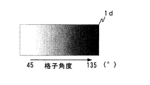
図3を参照して、格子角度を連続的に変化させた場合の階調について説明する。
回折格子を形成するドットの格子密度、格子ピッチを一定にし、格子角度を連続的に変化させると、図3のようになる。
光回折構造1dの明るい領域は格子角度が45°に近い回折格子で、暗い領域は格子角度が135°に近い回折格子で形成されている。
With reference to FIG. 3, the gradation when the lattice angle is continuously changed will be described.
When the grating density and the grating pitch of the dots forming the diffraction grating are made constant and the grating angle is continuously changed, the result is as shown in FIG.
The bright region of the optical diffraction structure 1d is formed by a diffraction grating having a grating angle close to 45 °, and the dark region is formed by a diffraction grating having a grating angle close to 135 °.
図4を参照して、従来の光回折構造の一例について説明する。
図2,図3で説明した回折格子を構成するドットの格子密度,格子ピッチ,格子角度の何れか二つを固定して、残りの要素だけを変化させてグラデーション図柄を作成すると図のようになる。
光回折構造2が濃淡のある背景図柄で構成され、その前方にやはり濃淡のある前景図柄を重ねると、一応の立体図柄を表現することができるが、図柄全体が静的な感じになってしまい、動きがある感じを表現することが難しい。
An example of a conventional light diffraction structure will be described with reference to FIG.
As shown in the figure, a gradation pattern is created by fixing only the remaining elements and fixing the grating density, grating pitch, and grating angle of the dots constituting the diffraction grating described in FIGS. Become.
If the light
図5を参照して、本発明の光回折構造の一例について説明する。
図5に示す光回折構造3の例は、回折格子を構成するドットの格子密度,格子ピッチ,格子角度の中の格子密度を固定して、残りの要素である格子ピッチ,格子角度を変化させて正方形を描写したものである。
光回折構造3の例は、正方形に内接する円の外側の格子ピッチを、例えば、1μm以下とし、内接する円の内側に向けて格子ピッチを広げ、中心付近の格子ピッチを、例えば、3.5μmとした例である。
図1のa図で説明したセルの集合を4個寄せ合わせて形成することもできるが、正方形の中心から同一の距離にあるセルを、格子ピッチを共通にして、格子角度を変えて形成することもできる。
An example of the light diffraction structure of the present invention will be described with reference to FIG.
In the example of the
In the example of the
Although it is possible to form a set of four cells as illustrated in FIG. 1a, the cells at the same distance from the center of the square are formed with a common lattice pitch and different lattice angles. You can also.
図5のc図と、表1を参照して、上述の内容ついて詳細に説明する。
格子ピッチと格子角度が同時に、連続的に変化する領域において、回折格子の格子角度が連続的に変化する方向を外周方向に定義し、回折格子の格子ピッチが連続的に変化する方向を外周から中心に向かう方向で定義することで、その扇形領域内は、中心に向かう方向にグラデーション効果が発生し、あたかも、円の中心に向かって光が流れ込んでゆくような光回折構造が得られる。
c図において、正方形の中心から正方形の上辺に直交する線分上の、座標「A1」のセルの回折格子を、表1に示すように、格子角度90度,格子ピッチ1.7μmで作成する。そして、正方形の中心から座標「A1」の距離上に存在する円周上のセル「A2」、「A3」,「A4」,「A5」,「A6」、「A7」,「A8」を、1.7μm(共通)の格子ピッチで、格子角度を連続的に変化させたセルとする。
同様に、正方形の中心から座標「B1」の距離上に存在する円周上のセル「B2」、「B3」,「B4」,「B5」,「B6」、「B7」,「B8」を、2.5μm(共通)の格子ピッチで、格子角度を連続的に変化させたセルとする。
前記、座標「A1」,「A2」、「A3」,「A4」,「A5」,「A6」、「A7」,「A8」、および、「B1」,「B2」、「B3」,「B4」,「B5」,「B6」、「B7」,「B8」のセルの格子角度は、表に記載の数値の如く変化させる。
ちなみに、「A1」,「B1」、「A5」,「B5」は正方形を縦に二分する線分上の座標,「A3」,「B3」、「A7」,「B7」は正方形を横に二分する線分上の座標,「A2」,「B2」,「A6」,「B6」、および、「A4」,「B4」、「A8」,「B8」は正方形の対角線上の座標,である。
With reference to FIG. 5c and Table 1, the above contents will be described in detail.
In a region where the grating pitch and the grating angle change continuously at the same time, the direction in which the grating angle of the diffraction grating changes continuously is defined as the outer circumferential direction, and the direction in which the grating pitch of the diffraction grating changes continuously from the outer circumference. By defining in the direction toward the center, a gradation effect is generated in the sector-shaped region in the direction toward the center, and an optical diffraction structure in which light flows into the center of the circle is obtained.
In FIG. c, as shown in Table 1, a diffraction grating of a cell with coordinates “A1” on a line segment orthogonal to the upper side of the square from the center of the square is created with a grating angle of 90 degrees and a grating pitch of 1.7 μm. . Then, the cells “A2”, “A3”, “A4”, “A5”, “A6”, “A7”, “A8” on the circumference existing at the coordinates “A1” from the center of the square are A cell in which the lattice angle is continuously changed at a lattice pitch of 1.7 μm (common) is used.
Similarly, the cells “B2”, “B3”, “B4”, “B5”, “B6”, “B7”, “B8” on the circumference existing at the coordinates “B1” from the center of the square. , A cell in which the lattice angle is continuously changed at a lattice pitch of 2.5 μm (common).
The coordinates “A1”, “A2”, “A3”, “A4”, “A5”, “A6”, “A7”, “A8”, and “B1”, “B2”, “B3”, “ The lattice angles of the cells “B4”, “B5”, “B6”, “B7”, and “B8” are changed as shown in the table.
By the way, “A1”, “B1”, “A5”, “B5” are the coordinates on the line segment that bisects the square vertically, “A3”, “B3”, “A7”, “B7” are horizontal The coordinates on the bisecting line segment, “A2”, “B2”, “A6”, “B6”, and “A4”, “B4”, “A8”, “B8” are the coordinates on the diagonal of the square is there.
試作データによれば、回折格子ピッチを2.0μm以上とした領域は、入射光を反射,回折する割合が減り、あたかも光を吸収しているように見える。
その結果、回折格子のピッチを連続的に変化させる際に、格子のピッチを2.0μm以上とすれば、あたかも2.0μm以上の格子ピッチの領域に向かって光が吸い込まれていくかのような、グラデーション効果を有する光回折構造を得ることができる。
According to the prototype data, in the region where the diffraction grating pitch is 2.0 μm or more, the ratio of reflecting and diffracting incident light decreases, and it seems as if light is absorbed.
As a result, when the pitch of the diffraction grating is continuously changed, if the pitch of the grating is set to 2.0 μm or more, it is as if light is sucked into a region having a grating pitch of 2.0 μm or more. In addition, a light diffraction structure having a gradation effect can be obtained.
特殊印刷物向けとして、高額な商品の包装材,パンフレット,POP、書籍の表紙等に貼付して使用する分野がある。
また、偽造防止向けとして、例えば、クレジットカード,IDカード等のカード類や商品券,小切手,手形,株券,入場券等の金券類、各種証明書等に貼付して使用する分野がある。
For special printed materials, there are fields where high-priced product packaging materials, pamphlets, POPs, book covers and the like are used.
For prevention of counterfeiting, for example, there are fields that are used by attaching to cards such as credit cards and ID cards, gift certificates, checks, bills, stock certificates, admission tickets, and various certificates.
1,1c,1d 光回折構造
2 従来の光回折構造の一例
3 本発明の光回折構造の一例
10 セル
21 背景図柄
22 前景図柄
100 ドット
P 格子ピッチ
α 格子角度
1, 1c, 1d
Claims (3)
回折格子の集合の少なくとも一部に、回折格子の格子ピッチと格子角度が同時に、かつ、連続的に変化する領域を有することを特徴とする光回折構造図。 A light diffraction structure formed by a set of diffraction gratings,
The optical diffraction structure figure which has the area | region where the grating | lattice pitch and grating | lattice angle of a diffraction grating change simultaneously and continuously in at least one part of the aggregate | assembly of a diffraction grating.
回折格子の格子ピッチと格子角度が共に、連続的に変化する領域において、回折格子の格子角度が連続的に変化する方向が円周方向に定義され、回折格子の格子ピッチが連続的に変化する方向がその法線方向で定義されたことを特徴とする光回折構造図。 In the light diffraction structure according to claim 1,
In the region where both the grating pitch and the grating angle of the diffraction grating continuously change, the direction in which the grating angle of the diffraction grating continuously changes is defined as the circumferential direction, and the grating pitch of the diffraction grating changes continuously. The light diffraction structure figure characterized by the direction being defined by the normal direction.
The optical diffraction structure according to any one of claims 1 and 2, wherein the grating pitch of the diffraction grating is in the range of 0.4 to 5.0 µm.
Priority Applications (1)
| Application Number | Priority Date | Filing Date | Title |
|---|---|---|---|
| JP2006166884A JP2007334076A (en) | 2006-06-16 | 2006-06-16 | Optical diffraction structure |
Applications Claiming Priority (1)
| Application Number | Priority Date | Filing Date | Title |
|---|---|---|---|
| JP2006166884A JP2007334076A (en) | 2006-06-16 | 2006-06-16 | Optical diffraction structure |
Publications (1)
| Publication Number | Publication Date |
|---|---|
| JP2007334076A true JP2007334076A (en) | 2007-12-27 |
Family
ID=38933602
Family Applications (1)
| Application Number | Title | Priority Date | Filing Date |
|---|---|---|---|
| JP2006166884A Pending JP2007334076A (en) | 2006-06-16 | 2006-06-16 | Optical diffraction structure |
Country Status (1)
| Country | Link |
|---|---|
| JP (1) | JP2007334076A (en) |
Cited By (1)
| Publication number | Priority date | Publication date | Assignee | Title |
|---|---|---|---|---|
| JP2016206589A (en) * | 2015-04-28 | 2016-12-08 | 凸版印刷株式会社 | Display body and article with label |
Citations (3)
| Publication number | Priority date | Publication date | Assignee | Title |
|---|---|---|---|---|
| US4568141A (en) * | 1982-10-04 | 1986-02-04 | Lgz Landis & Gyr Zug Ag | Document having an optical-diffraction authenticating element |
| JPH09506442A (en) * | 1993-11-23 | 1997-06-24 | コモンウェルス・サイエンティフィック・アンド・インダストリアル・リサーチ・オーガナイゼーション | Diffraction mark for surface |
| WO2005009751A2 (en) * | 2003-07-22 | 2005-02-03 | Giesecke & Devrient Gmbh | Security element |
-
2006
- 2006-06-16 JP JP2006166884A patent/JP2007334076A/en active Pending
Patent Citations (3)
| Publication number | Priority date | Publication date | Assignee | Title |
|---|---|---|---|---|
| US4568141A (en) * | 1982-10-04 | 1986-02-04 | Lgz Landis & Gyr Zug Ag | Document having an optical-diffraction authenticating element |
| JPH09506442A (en) * | 1993-11-23 | 1997-06-24 | コモンウェルス・サイエンティフィック・アンド・インダストリアル・リサーチ・オーガナイゼーション | Diffraction mark for surface |
| WO2005009751A2 (en) * | 2003-07-22 | 2005-02-03 | Giesecke & Devrient Gmbh | Security element |
Cited By (1)
| Publication number | Priority date | Publication date | Assignee | Title |
|---|---|---|---|---|
| JP2016206589A (en) * | 2015-04-28 | 2016-12-08 | 凸版印刷株式会社 | Display body and article with label |
Similar Documents
| Publication | Publication Date | Title |
|---|---|---|
| EP1782108B1 (en) | A method of creating a three-dimensional image, a diffractive element and method of creating the same | |
| RU2491595C2 (en) | Protective element and method of making protective element | |
| US7710652B2 (en) | Grid image with one or several grid fields | |
| CN101952127B (en) | Film element | |
| JP4983899B2 (en) | Display and labeled goods | |
| CN111132852A (en) | Optical switching device | |
| JP4831320B2 (en) | Authenticity identification structure | |
| JP5143855B2 (en) | Display and labeled goods | |
| GB2523888A (en) | Security elements and methods of their manufacture | |
| TW200842052A (en) | Security element for a security document and method for production thereof | |
| JPH02165987A (en) | Optically variable face pattern | |
| JP5720099B2 (en) | Display body, article with display body, method for manufacturing original plate, method for manufacturing stamper, and method for manufacturing display body | |
| JP5504732B2 (en) | Display and labeled goods | |
| JP2007223100A (en) | Information printed matter | |
| JP5163137B2 (en) | Display body and article with display body | |
| JP4831321B2 (en) | Hidden information by uneven structure | |
| CN104210273A (en) | Volume reflection holographic anti-counterfeiting element and economic goods | |
| JP4844822B2 (en) | Authenticity identification structure | |
| CA2417795A1 (en) | Optically active structure for personalizing cards and the like, and method for the production thereof | |
| JP2010286722A (en) | Display body and article with label | |
| JP2007309960A (en) | Display and method for manufacturing the same | |
| JP4848852B2 (en) | Light diffraction structure | |
| JP2008026459A (en) | Light diffracting structure and tool for discriminating hidden information | |
| JP2009134093A (en) | Diffraction structure, forgery prevention medium using the same, and forgery prevention paper | |
| JP2008039889A (en) | Concealed image by uneven microstructure |
Legal Events
| Date | Code | Title | Description |
|---|---|---|---|
| A621 | Written request for application examination |
Free format text: JAPANESE INTERMEDIATE CODE: A621 Effective date: 20090528 |
|
| A977 | Report on retrieval |
Free format text: JAPANESE INTERMEDIATE CODE: A971007 Effective date: 20110420 |
|
| A131 | Notification of reasons for refusal |
Free format text: JAPANESE INTERMEDIATE CODE: A131 Effective date: 20110510 |
|
| A521 | Request for written amendment filed |
Free format text: JAPANESE INTERMEDIATE CODE: A523 Effective date: 20110624 |
|
| A02 | Decision of refusal |
Free format text: JAPANESE INTERMEDIATE CODE: A02 Effective date: 20110816 |