JP2007294088A - Magnetic write head which makes projection induced thermally decrease, and its manufacturing method - Google Patents
Magnetic write head which makes projection induced thermally decrease, and its manufacturing method Download PDFInfo
- Publication number
- JP2007294088A JP2007294088A JP2007096452A JP2007096452A JP2007294088A JP 2007294088 A JP2007294088 A JP 2007294088A JP 2007096452 A JP2007096452 A JP 2007096452A JP 2007096452 A JP2007096452 A JP 2007096452A JP 2007294088 A JP2007294088 A JP 2007294088A
- Authority
- JP
- Japan
- Prior art keywords
- coil
- layer
- magnetic
- write
- photoresist
- Prior art date
- Legal status (The legal status is an assumption and is not a legal conclusion. Google has not performed a legal analysis and makes no representation as to the accuracy of the status listed.)
- Pending
Links
- 230000005291 magnetic effect Effects 0.000 title claims abstract description 150
- 238000004519 manufacturing process Methods 0.000 title claims description 16
- 229920002120 photoresistant polymer Polymers 0.000 claims abstract description 54
- NJPPVKZQTLUDBO-UHFFFAOYSA-N novaluron Chemical compound C1=C(Cl)C(OC(F)(F)C(OC(F)(F)F)F)=CC=C1NC(=O)NC(=O)C1=C(F)C=CC=C1F NJPPVKZQTLUDBO-UHFFFAOYSA-N 0.000 claims abstract description 43
- PNEYBMLMFCGWSK-UHFFFAOYSA-N aluminium oxide Inorganic materials [O-2].[O-2].[O-2].[Al+3].[Al+3] PNEYBMLMFCGWSK-UHFFFAOYSA-N 0.000 claims abstract description 28
- 238000009413 insulation Methods 0.000 claims abstract description 18
- 239000000463 material Substances 0.000 claims abstract description 9
- 238000004804 winding Methods 0.000 claims abstract description 9
- 238000000034 method Methods 0.000 claims description 19
- 230000015572 biosynthetic process Effects 0.000 claims description 6
- 239000004020 conductor Substances 0.000 claims description 6
- 230000008569 process Effects 0.000 claims description 6
- 239000000945 filler Substances 0.000 claims description 5
- 239000000696 magnetic material Substances 0.000 claims description 5
- 238000000206 photolithography Methods 0.000 claims description 4
- 238000010438 heat treatment Methods 0.000 claims description 3
- 230000008878 coupling Effects 0.000 claims description 2
- 238000010168 coupling process Methods 0.000 claims description 2
- 238000005859 coupling reaction Methods 0.000 claims description 2
- 238000000151 deposition Methods 0.000 claims 7
- 238000000059 patterning Methods 0.000 claims 3
- 239000012777 electrically insulating material Substances 0.000 claims 2
- 238000003892 spreading Methods 0.000 claims 1
- 239000000758 substrate Substances 0.000 claims 1
- 239000010410 layer Substances 0.000 description 98
- 230000004907 flux Effects 0.000 description 8
- 239000000725 suspension Substances 0.000 description 6
- 230000005415 magnetization Effects 0.000 description 5
- 238000003860 storage Methods 0.000 description 5
- 229910003321 CoFe Inorganic materials 0.000 description 4
- 229910001030 Iron–nickel alloy Inorganic materials 0.000 description 4
- 230000008859 change Effects 0.000 description 4
- 229910018072 Al 2 O 3 Inorganic materials 0.000 description 3
- 230000005294 ferromagnetic effect Effects 0.000 description 3
- 238000005339 levitation Methods 0.000 description 3
- 238000001020 plasma etching Methods 0.000 description 3
- 239000011241 protective layer Substances 0.000 description 3
- 125000006850 spacer group Chemical group 0.000 description 3
- 230000002411 adverse Effects 0.000 description 2
- 230000008901 benefit Effects 0.000 description 2
- 239000003989 dielectric material Substances 0.000 description 2
- 238000009713 electroplating Methods 0.000 description 2
- 230000006870 function Effects 0.000 description 2
- 239000011810 insulating material Substances 0.000 description 2
- 239000000126 substance Substances 0.000 description 2
- 229910045601 alloy Inorganic materials 0.000 description 1
- 239000000956 alloy Substances 0.000 description 1
- 230000000712 assembly Effects 0.000 description 1
- 238000000429 assembly Methods 0.000 description 1
- 238000004590 computer program Methods 0.000 description 1
- 239000002772 conduction electron Substances 0.000 description 1
- 230000007797 corrosion Effects 0.000 description 1
- 238000005260 corrosion Methods 0.000 description 1
- 235000019788 craving Nutrition 0.000 description 1
- 238000005520 cutting process Methods 0.000 description 1
- 238000001514 detection method Methods 0.000 description 1
- 238000010586 diagram Methods 0.000 description 1
- 230000005292 diamagnetic effect Effects 0.000 description 1
- 238000005530 etching Methods 0.000 description 1
- 238000007667 floating Methods 0.000 description 1
- 230000001939 inductive effect Effects 0.000 description 1
- 230000007787 long-term memory Effects 0.000 description 1
- 238000005498 polishing Methods 0.000 description 1
- 230000009467 reduction Effects 0.000 description 1
- 230000004044 response Effects 0.000 description 1
- 229910000702 sendust Inorganic materials 0.000 description 1
- 239000002344 surface layer Substances 0.000 description 1
Images


Classifications
-
- G—PHYSICS
- G11—INFORMATION STORAGE
- G11B—INFORMATION STORAGE BASED ON RELATIVE MOVEMENT BETWEEN RECORD CARRIER AND TRANSDUCER
- G11B5/00—Recording by magnetisation or demagnetisation of a record carrier; Reproducing by magnetic means; Record carriers therefor
- G11B5/127—Structure or manufacture of heads, e.g. inductive
- G11B5/1278—Structure or manufacture of heads, e.g. inductive specially adapted for magnetisations perpendicular to the surface of the record carrier
-
- G—PHYSICS
- G11—INFORMATION STORAGE
- G11B—INFORMATION STORAGE BASED ON RELATIVE MOVEMENT BETWEEN RECORD CARRIER AND TRANSDUCER
- G11B5/00—Recording by magnetisation or demagnetisation of a record carrier; Reproducing by magnetic means; Record carriers therefor
- G11B5/127—Structure or manufacture of heads, e.g. inductive
- G11B5/31—Structure or manufacture of heads, e.g. inductive using thin films
- G11B5/3109—Details
- G11B5/313—Disposition of layers
- G11B5/3133—Disposition of layers including layers not usually being a part of the electromagnetic transducer structure and providing additional features, e.g. for improving heat radiation, reduction of power dissipation, adaptations for measurement or indication of gap depth or other properties of the structure
- G11B5/3136—Disposition of layers including layers not usually being a part of the electromagnetic transducer structure and providing additional features, e.g. for improving heat radiation, reduction of power dissipation, adaptations for measurement or indication of gap depth or other properties of the structure for reducing the pole-tip-protrusion at the head transducing surface, e.g. caused by thermal expansion of dissimilar materials
Abstract
Description
本発明は磁気データ記録に関し、より具体的には、磁気書き込みヘッドにおける、熱的に誘発される磁極端の変形を防止する構造及びヘッドの製造方法に関する。 The present invention relates to magnetic data recording, and more particularly to a structure and a head manufacturing method that prevent thermally induced magnetic pole tip deformation in a magnetic write head.
コンピュータにおける長期記憶の中心は、磁気ディスクドライブと呼ばれる組み立て品である。磁気ディスクドライブは、回転する磁気ディスク、回転する磁気ディスクの表面に隣接する1個のサスペンションアームに吊り下げられている書き込みヘッドと読み取りヘッド、及びサスペンションアームを動かして、読み取りヘッド及び書き込みヘッドを回転ディスク上の選択された環状トラック上に位置決めするためのアクチュエータを含んでいる。読み取りヘッド及び書き込みヘッドは、空気ベアリング表面 (ABS) を持つスライダ上に直接位置している。サスペンションアームは、スライダをディスク表面に向かって偏らせ、ディスクが回転する時、ディスク近傍の空気はディスク表面と共に移動する。スライダは、この移動する空気のクッションに隔てられてディスク表面上に浮揚する。スライダが空気ベアリング上に浮いている時、書き込みヘッド及び読み取りヘッドは、回転ディスクに磁気変化を書き込み、回転ディスクから磁気変化を読み取る。読み取りヘッド及び書き込みヘッドは、コンピュータ・プログラムに従って書き込み機能及び読み取り機能を実行させるように働く処理回路に接続されている。 The center of long-term memory in computers is an assembly called a magnetic disk drive. The magnetic disk drive rotates the read head and the write head by moving the rotating magnetic disk, the write head and the read head suspended on one suspension arm adjacent to the surface of the rotating magnetic disk, and the suspension arm. It includes an actuator for positioning on a selected annular track on the disk. The read head and write head are located directly on a slider having an air bearing surface (ABS). The suspension arm biases the slider toward the disk surface, and when the disk rotates, the air near the disk moves with the disk surface. The slider floats on the disk surface, separated by this moving air cushion. When the slider is floating over the air bearing, the write head and read head write magnetic changes to the rotating disk and read magnetic changes from the rotating disk. The read head and write head are connected to processing circuitry that serves to perform the write and read functions in accordance with a computer program.
書き込みヘッドは、伝統的に1個以上の絶縁層(絶縁スタック)内に埋め込まれた1個のコイル層を持っており、絶縁スタックは第1及び第2の磁極片層の間に挟まれている。書き込みヘッドの空気ベアリング表面 (ABS) では、第1及び第2の磁極片層の間に1個のギャップ層によってギャップが形成されており、2個の磁極片層はバックギャップで連結されている。コイル層に通じられる電流が磁極片内に磁束を誘起させ、この磁束は、移動する記録媒体のトラック、例えば前述した回転ディスク上の環状トラックなどに前記の磁気的変化を書き込む目的でABSにおける書き込みギャップから磁場を房状に流出させる。 A write head traditionally has a coil layer embedded in one or more insulating layers (insulating stack), the insulating stack being sandwiched between first and second pole piece layers. Yes. On the air bearing surface (ABS) of the write head, a gap is formed by a gap layer between the first and second pole piece layers, and the two pole piece layers are connected by a back gap. . The current passed through the coil layer induces a magnetic flux in the pole piece, which is written in ABS for the purpose of writing the magnetic change on the track of the moving recording medium, such as the annular track on the rotating disk mentioned above. The magnetic field flows out from the gap in a tufted manner.
現在行われている読み取りヘッドの設計では、回転している磁気ディスクからの磁場を検知するために、スピンバルブ・センサ(GMRセンサとも呼ばれる)が使用されるようになっている。このセンサは、第1及び第2の強磁性層(以下、それぞれ固定層及び自由層と呼ぶ)の間に挟まれた1個の非磁性導電層(以下、スペーサ層と呼ぶ)を含んでいる。スピンバルブ・センサには、検知電流を通じるために第1及び第2のリード導体が連結されている。固定層の磁化は、空気ベアリング表面 (ABS) に対し垂直に固定されており、自由層の磁気モーメントはABSに平行であるが、外部磁場に応じて自由に回転することができる。固定層の磁化は、典型的には反磁性層との交換カップリングによって固定される。 Current readhead designs use spin valve sensors (also called GMR sensors) to detect the magnetic field from a rotating magnetic disk. This sensor includes one nonmagnetic conductive layer (hereinafter referred to as a spacer layer) sandwiched between first and second ferromagnetic layers (hereinafter referred to as a fixed layer and a free layer, respectively). . First and second lead conductors are connected to the spin valve sensor in order to pass a detection current. The magnetization of the fixed layer is fixed perpendicular to the air bearing surface (ABS) and the magnetic moment of the free layer is parallel to the ABS, but can rotate freely in response to an external magnetic field. The magnetization of the pinned layer is typically pinned by exchange coupling with the diamagnetic layer.
スペーサ層の厚さは、センサを通る伝導電子の平均自由行路よりも小さくなるように選ばれる。このように配置すれば、電導電子の一部は、スペーサ層と固定層及び自由層のそれぞれの界面で散乱される。固定層と自由層の磁化が互いに平行ならば散乱は最小であり、固定層と自由層の磁化が逆平行ならば散乱は最大である。散乱の変化は、スピンバルブ・センサの抵抗を cos θ に比例して変化させる。ここで θ は固定層と自由層の磁化の間の角度である。読み取りモードでは、スピンバルブ・センサの抵抗は回転ディスクから発する磁場の大きさに比例して変化する。検知電流がスピンバルブ・センサに通じられると、抵抗の変化によって電位の変化が生じ、それが検出されてプレイバック信号として処理される。 The thickness of the spacer layer is chosen to be smaller than the mean free path of conduction electrons through the sensor. With this arrangement, a part of the electric conductor is scattered at each interface between the spacer layer, the fixed layer, and the free layer. Scattering is minimal when the magnetizations of the fixed and free layers are parallel to each other, and scattering is maximum when the magnetizations of the fixed and free layers are antiparallel. The change in scattering changes the resistance of the spin valve sensor in proportion to cos θ. Where θ is the angle between the magnetization of the fixed layer and the free layer. In read mode, the resistance of the spin valve sensor changes in proportion to the magnitude of the magnetic field emanating from the rotating disk. When the sense current is passed to the spin valve sensor, a change in potential occurs due to a change in resistance, which is detected and processed as a playback signal.
スピンバルブ・センサは第1及び第2の非磁性で電気絶縁性の読み取りギャップ層の間に位置しており、第1及び第2の読み取りギャップ層は強磁性の第1及び第2シールド層の間に位置している。合体型磁気ヘッドでは、単一の強磁性層が、読み取りヘッドのシールド層として、また書き込みヘッドの第1磁極片層として機能する。ピギーバック型ヘッドでは、第2のシールド層と第1の磁極片層は別々の層である。 The spin valve sensor is located between the first and second non-magnetic, electrically insulating read gap layers, the first and second read gap layers being the ferromagnetic first and second shield layer layers. Located between. In the combined magnetic head, a single ferromagnetic layer functions as a shield layer for the read head and as a first pole piece layer for the write head. In the piggyback head, the second shield layer and the first pole piece layer are separate layers.
ごく最近、研究者たちの開発努力は、記録システムのデータ密度を高めるために、垂直磁気記録システムの開発に集中されている。このような垂直記録システムは、データの磁気的ビットを、磁気記録媒体の表面に対し垂直な方向に記録する。一般に、かかるシステムに使用される書き込みヘッドは、空気ベアリング表面 (ABS) における断面が比較的小さい書き込み磁極と、ABSにおける断面がそれより大きな戻り磁極を備えている。磁気書き込みコイルに誘起される磁束は、一般に磁気記録媒体の面に垂直な方向に放射される。この磁束は戻り磁極で書き込みヘッドに戻るが、その際には磁束は十分に拡散して弱まっており、書き込み磁極によって書き込まれた信号を消去することはない。 Most recently, researchers' development efforts have been concentrated on the development of perpendicular magnetic recording systems in order to increase the data density of the recording systems. Such perpendicular recording systems record magnetic bits of data in a direction perpendicular to the surface of the magnetic recording medium. In general, write heads used in such systems have a write pole with a relatively small cross section at the air bearing surface (ABS) and a return pole with a larger cross section at the ABS. The magnetic flux induced in the magnetic writing coil is generally radiated in a direction perpendicular to the surface of the magnetic recording medium. This magnetic flux returns to the write head by the return magnetic pole, but at this time, the magnetic flux is sufficiently diffused and weakened, and the signal written by the write magnetic pole is not erased.
データ速度とデータ容量の向上に対する年々強まる要求に応じるために、研究者たちは、読み取りヘッド及び書き込みヘッドのサイズを小さくしながら、そのような書き込みヘッドによって生ずる書き込み磁場を強める方策を、絶えず求め続けている。書き込み磁場を強めるためには、書き込みコイルを流れる電流を増さねばならない。書き込みヘッドのサイズを小さくするためには書き込みコイルのサイズ縮小(コイルの断面積の縮小)が必要であり、それはコイルの電気抵抗を増大させる。 In order to meet the ever-increasing demands for increased data rates and data capacities, researchers are constantly seeking ways to increase the write magnetic field generated by such write heads while reducing the size of the read and write heads. ing. In order to increase the write magnetic field, the current flowing through the write coil must be increased. In order to reduce the size of the write head, it is necessary to reduce the size of the write coil (reducing the cross-sectional area of the coil), which increases the electrical resistance of the coil.
このサイズ縮小と書き込み電流の増大のために、使用中に書き込みヘッドによって発生する熱量が大幅に増大する。この熱は書き込みヘッドの望ましくない熱膨張を惹き起こし、場合によっては書き込みヘッド構造の破局的な変形をもたらすおそれがある。この変形は、ヘッドの浮揚する高さが並外れて小さく、ナノメートルのオーダーになる現在及び未来の磁気ヘッドの場合、特に問題となる。書き込みヘッドの熱膨張による突出がこの低い浮揚の高さと相俟って、使用中にヘッドとディスクが破局的に接触するという結果に至るおそれがある。それ故、小型で高出力の書き込みヘッドにおいて、そのような熱によって誘発される変形を回避する手段が強く渇望されている。 This reduction in size and increase in write current greatly increases the amount of heat generated by the write head during use. This heat can cause undesired thermal expansion of the write head and in some cases can lead to catastrophic deformation of the write head structure. This deformation is particularly problematic for current and future magnetic heads where the flying height of the head is exceptionally small and on the order of nanometers. The protrusion due to thermal expansion of the write head, coupled with this low levitation height, can result in catastrophic contact between the head and the disk during use. Therefore, there is a strong craving for a means to avoid such heat-induced deformation in small and high power write heads.
本発明は、熱によって誘発される変形を起こし難い、垂直磁気記録用の磁気書き込みヘッドを提供するものである。この書き込みヘッドは、それぞれ一端が空気ベアリング表面 (ABS) に配置されている書き込み磁極と戻り磁極を有する。磁気ペデスタルが戻り磁極のABS端に形成され、書き込み磁極に向かって広がる。複数のコイル巻き線を有する導電性の書き込みコイルが戻り磁極の上を通っており、非磁性で電気絶縁性の充填材が書き込みコイルとペデスタルの間の空間を満たしている。充填材は熱膨張係数が低い、例えばアルミナのような材料で構成されている。 The present invention provides a magnetic write head for perpendicular magnetic recording that is less prone to heat-induced deformation. The write head has a write pole and a return pole, each of which is disposed at one end on the air bearing surface (ABS). A magnetic pedestal is formed at the ABS end of the return pole and extends toward the write pole. A conductive write coil having a plurality of coil windings passes over the return pole and a non-magnetic, electrically insulating filler fills the space between the write coil and the pedestal. The filler is made of a material having a low coefficient of thermal expansion, such as alumina.
コイルの巻き線間にフォトレジストのコイル絶縁層を設け、コイルの巻き線相互間を絶縁することができる。また、ヘッドは、戻り磁極のABSから遠い側の端に形成されたバックギャップを含んでも良い。磁気バックギャップ層は、磁気形成層によって書き込み磁極と磁気的に結合されていても良い。 A coil insulating layer of a photoresist can be provided between the coil windings to insulate the coil windings from each other. Further, the head may include a back gap formed at an end of the return magnetic pole far from the ABS. The magnetic back gap layer may be magnetically coupled to the write pole by a magnetic forming layer.
フォトレジストの絶縁層は、コイルとバックギャップ層の間に広がっていて良く、非磁性で導電性であり、熱膨張率の低い充填層は書き込みコイルとコイル絶縁層の上を通り、バックギャップ層まで広がっていて良い。 The insulating layer of the photoresist may extend between the coil and the back gap layer, is non-magnetic and conductive, and the filling layer having a low coefficient of thermal expansion passes over the writing coil and the coil insulating layer, and the back gap layer It may be spread to.
充填層の熱膨張係数は低いので、例えば書き込みコイルから発生するジュール熱などで加熱されても、ペデスタルを圧迫し変形させることがないという利点がある。例えば、フォトレジストはアルミナよりもはるかに大きな熱膨張係数を持つ。フォトレジストの絶縁層でコイルとペデスタルの間の空間を満たすことを許容するならば、このフォトレジスト層は加熱された際に膨張し、ペデスタルを圧迫してペデスタルの塑性変形を起こし、ペデスタルをディスクに向かって突出させて、遂にはヘッドとディスクの接触を招くおそれがあるし、そうならぬ迄も書き込みヘッドの性能に悪影響を及ぼす。それ故に本発明は、熱によって誘発される書き込みヘッドの変形を防止し、優れた書き込みヘッド性能と信頼性を保証するものである。 Since the thermal expansion coefficient of the packed layer is low, there is an advantage that the pedestal is not compressed and deformed even when heated by, for example, Joule heat generated from the writing coil. For example, photoresist has a much larger coefficient of thermal expansion than alumina. If it is possible to fill the space between the coil and the pedestal with an insulating layer of photoresist, this photoresist layer will expand when heated, compressing the pedestal, causing plastic deformation of the pedestal, The head and the disk may eventually come into contact with each other, and otherwise the write head performance will be adversely affected. Therefore, the present invention prevents write head deformation induced by heat and ensures excellent write head performance and reliability.
本発明のこれらの特徴及びその他の特徴は、次節の好ましい実施形態の説明を、添付図面と関連させて読むことによって明らかになるであろう。すべての図面を通じて、同じ参照数字は同類の構成要素を示す。 These and other features of the present invention will become apparent from the following description of the preferred embodiment read in conjunction with the accompanying drawings. Throughout the drawings, the same reference numerals indicate similar components.
本発明によれば、熱によって誘発される書き込みヘッドの変形を防止し、優れた書き込みヘッド性能と信頼性を保証することができる。 According to the present invention, the deformation of the write head induced by heat can be prevented, and excellent write head performance and reliability can be ensured.
以下の説明は、本発明を実施するに当たって今日考えられる最善の実施形態の説明である。この説明は本発明の一般原理を例示する目的で行われるものであり、本明細書中に主張されている発明の概念を限定する意図によるものではない。 The following is a description of the best embodiments contemplated today for practicing the present invention. This description is made for the purpose of illustrating the general principles of the invention and is not intended to limit the inventive concepts claimed herein.
本発明の性格と長所、及び好ましい使用態様のより完全な理解のために、以下の詳細な説明を添付図面と関連させて読み、参照されたい。但し添付図面は一定の拡大率によったものではない。 For a more complete understanding of the nature and advantages of the present invention and the preferred modes of use, read and refer to the following detailed description in conjunction with the accompanying drawings. However, the attached drawings are not based on a certain enlargement ratio.
さて、図1には、本発明を具体的に例示するディスクドライブ100が示されている。図1に示されるように、1個以上の回転可能な磁気記録ディスク112がスピンドル114に支えられ、ディスク駆動モータ118によって回転せしめられる。それぞれのディスクにおける磁気記録は、磁気記録ディスク112上の同心円状データトラック(図示されていない)の環状パターンの形をなしている。
FIG. 1 shows a
磁気記録ディスク112の近傍に1個以上のスライダ113が位置決めされており、それぞれのスライダ113は1個以上の磁気記録ヘッド・アセンブリ121を担持している。磁気記録ディスクが回転する間にスライダ113はディスク表面122上を半径に沿って内外に移動するので、磁気記録ヘッド・アセンブリ121は磁気記録ディスクの種々異なったトラックにアクセスし、そこで所望のデータ書き込みを行うことができる。それぞれのスライダ113は、サスペンション115によってアクチュエータ・アーム119に取り付けられている。サスペンション115には弱い発条力があり、それがスライダ113をディスク表面122の方向に偏向させている。それぞれのアクチュエータ・アーム119はアクチュエータ手段127に取り付けられている。図1に示されているようなアクチュエータ手段127は、ボイスコイル・モータ (VCM) であって良い。VCMは固定磁場内を移動できるコイルを含んでおり、コイル移動の方向と速度は、制御装置129によって供給されるモータ電流信号によって制御される。
One or
ディスク記憶システムの作動中、磁気記録ディスク112の回転によってスライダ113とディスク表面122の間に空気ベアリングが生じ、それがスライダに対し上向きの力、すなわち浮揚力を及ぼす。かくして空気ベアリングは、サスペンション115の弱い発条力を浮揚力によって打消し、正常な作動の間、スライダ113をディスク表面の上方に、実質的に一定の小さな間隔を置いて支える。
During operation of the disk storage system, rotation of the
ディスク記憶システムの種々の構成部分は、作動中、制御ユニット129が発生する制御信号、例えばアクセス制御信号、内部クロック信号などによって制御される。典型的には、制御ユニット129は論理制御回路、記憶手段、及びマイクロプロセッサを含む。制御ユニット129は、制御信号を発生させ、駆動モータ制御信号の回線接続123 、ヘッドの位置、シーク制御信号の回線接続128などのような種々のシステムオペレーションを制御する。制御信号の回線接続128は、スライダ113を最適な態様で移動させ、ディスク112上の所望のデータトラックに位置決めするために、必要な電流プロファイルを供給する。書き込み信号及び読み取り信号は、記録チャネル125によって書き込みおよび読み取りヘッド121に伝送される。
Various components of the disk storage system are controlled by control signals generated by the
図2によって、スライダ113内における磁気ヘッド121の配置を、より詳細に見ることができる。図2はスライダ113をABS側から見た図であって、見られるように、1個の誘導書き込みヘッドを含む磁気ヘッドは、スライダの進行方向に対する後縁に位置している。典型的な磁気記録ディスク記憶システムに関する以上の説明と、添付の図1による例示は、代表例を示すために過ぎない。ディスク記憶システムが多数のディスク及びアクチュエータを含み、それぞれのアクチュエータが幾つものスライダを支えていても良いことは明白であろう。
2, the arrangement of the
さて、図3には、垂直磁気記録システム用の磁気ヘッド121が示されている。ヘッド121は、書き込み素子302及び読み取り素子304を含んでいる。読み取り素子304は、磁気抵抗読み取りセンサ305を含んでいる。このセンサ305は、例えば面平行電流GMRセンサ (CIP GMR) 、面垂直電流GMRセンサ (CPP GMR) 、またはトンネル接合センサ (TMR) であり得るであろう。センサ305は第1及び第2の磁気シールド306, 308の間に位置し、誘電性材料307中に埋め込まれている。磁気シールド306, 308は、例えばCoFe、NiFeあるいはセンダスト合金で構成され得るものであって、アップトラックあるいはダウントラックデータ信号に由来するような磁場を吸収し、読み取りセンサ305がシールド306, 307の間に位置するデータトラックだけを検出することを確実ならしめる。非磁性で電気絶縁性のギャップ層309が、シールド308と書き込みヘッド302の間に設けられていても良い。センサがCIP GMRセンサ305であるならば、図3に示されているように該センサはシールド306, 308から絶縁されるであろう。しかしながら、センサ305がCPP GMRセンサ、またはTMRセンサであるならば、センサ305の上部及び下部をシールド306, 308に接触せしめ、これらシールドがセンサ305に検知電流を供給するためのリード導電体として作用し得るようにすることができる。
FIG. 3 shows a
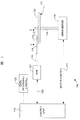
図3によって説明を続ける。書き込み素子302は、磁気的に磁気形成層312と結合され、絶縁材料311内に埋め込まれている書き込み磁極310を含んでいる。書き込み磁極310は空気ベアリング表面では小さな断面を持ち、磁性材料で構成されている。書き込みヘッド302は、CoFeあるいはNiFeなどのような磁性材料で構成された戻り磁極314を含んでおり、ABS面に平行な断面は、書き込み磁極310のそれよりもかなり大きい。図3に示されているように、戻り磁極314は形成層312及び書き込み磁極310と、バックギャップ部分316によって磁気的に結合されている。戻り磁極314及びバックギャップ316は、例えばNiFe、CoFe、あるいはその他の磁性材料で構成することができる。
The description will be continued with reference to FIG. The
導電性の書き込みコイル317(図3中には、断面で示してある)が、形成層312と戻り磁極314の間で書き込み素子302を貫いている。ヘッド121を腐食や磨耗などの損傷から保護するために、ヘッドの最上部に、例えばアルミナで構成された硬質で電気絶縁性の保護層322を設けても良い。
A conductive write coil 317 (shown in cross section in FIG. 3) penetrates the
コイル317に電流が通る時、その結果生ずる磁場のために、磁束が戻り磁極314、バックギャップ316、形成層312及び書き込み磁極310を通って流れる。この磁束が、隣接する磁気記録媒体(図示されていない)に向かって書き込み磁界を放射させる。書き込み磁極310から放射されるこの磁場が、磁気記録媒体(図3には示されていない)上にある、比較的保磁力が高く、薄い磁性表面層を磁化させる。この磁場は磁気記録媒体の軟磁性の下地層を通って戻り磁極314に達するが、そこでは磁束は十分に拡散しており、書き込み磁極310によって書き込まれた信号を消去することはない。
As current flows through the
さらに図3について述べれば、書き込みヘッド302は、磁気シールドすなわちペデスタル324を含んでも良い。この磁気ペデスタルは、NiFeやCoFeなどのような磁性材料で構成することができ、戻り磁極と磁気的に結合されていても良い。ペデスタル324は、書き込みコイル317から出る磁束が磁気記録媒体(図示されていない)に達して悪影響を及ぼすことを防止するためのシールドとして作用する。
Still referring to FIG. 3, the
コイル317は、戻り磁極314、バックギャップ316および形成層312から磁気的にも電気的にも絶縁されている。書き込みコイル317の下に下部絶縁層321が設けられ、書き込みコイル317をその下方にある戻り磁極314から絶縁している。コイル絶縁層328は、コイル317の巻き線の間の空間を充填し、またコイル317とバックギャップ316の間の空間も充填する。このコイル絶縁層は、コイル317の巻き線の間の微細で縦横比の大きな空間に容易に堆積せしめられ得るような材料で構成されることが好ましい。従って、コイル絶縁層328は、コイルの巻き線の間の小さな空間内に容易に堆積させ、その後、熱処理によって硬化させることができるフォトレジストであることが好ましい。しかしながら、見て取れるように、フォトレジストのコイル絶縁層328は、コイルとペデスタル324の間には広がらない。
The
引き続き図3によって述べれば、絶縁充填層330がコイル317とペデスタル324の間を充填し、かつコイル317の上方、コイル317と形成層312の間の空間をも充填することができる。また、絶縁層332が、形成層312とABSの間の空間を充填する。この絶縁層332は、絶縁充填層330と一体であっても、また別の部分であっても良い。好ましくは、絶縁層332はアルミナ (Al2O3) で構成される。この材料はABSにおいて、硬質で曝露耐久性のある表面となる故である。
Continuing with FIG. 3, the insulating
さらに図3を参照すれば、絶縁充填層330がコイル317とペデスタルの間の空間を充填していることが見て取れる。絶縁充填層は、電気絶縁性の、熱膨張係数が比較的小さい非磁性材料で構成される。例えば、該充填層330の材料としては、アルミナ (Al2O3) が優れている。この材料は熱膨張係数が小さく、硬質で、非磁性、非導電性であり、入手も容易である。フォトレジストで構成されているコイル絶縁層328は、アルミナの充填層330よりもはるかに熱膨張係数が大きいことを指摘したい。フォトレジストのコイル絶縁層がコイル317とペデスタル324の間にまで広がっているならば、フォトレジストのコイル絶縁層328の熱膨張が、ペデスタル324に過大な機械的応力が加わる原因となるであろう。このストレスが加われば、ペデスタルを変形(おそらく塑性的に)変形させ、ペデスタルをABSから外部に突出させるであろう。このペデスタル324の突出は、次いでディスク(図示されていない)との破局的な接触を惹き起こし、ディスクの損傷及びヘッドの損傷を起こす原因となり得るであろう。
Still referring to FIG. 3, it can be seen that the insulating
より古いタイプのコイル製作方式では、フォトレジストのコイル絶縁層を、該絶縁層がペデスタルまで広がるように施し、ペデスタル324をフォトレジスト層の前縁を定義するせき止め手段として利用する。しかるに本発明によれば、コイル317とペデスタル324の間の空間をアルミナのような熱膨張係数が小さい材料で充填するため、書き込みヘッド302の加熱による突出が大幅に軽減される。
In older types of coil fabrication systems, a photoresist coil insulation layer is applied so that the insulation layer extends to the pedestal, and the
図4〜図8を参照しつつ、本発明の一実施形態による書き込みヘッドの製作方法を説明する。特に図4では、読み取りヘッド304は既に構築済みであり、非磁性のギャップ層309が堆積され、戻り磁極314が形成される。次いで戻り磁極314上にペデスタル324とバックギャップ316が形成される。
A method for manufacturing a write head according to an embodiment of the present invention will be described with reference to FIGS. In particular, in FIG. 4, the
例えばアルミナで構成されている薄い電気絶縁性の非磁性層321が、戻り磁極314の上に堆積される。導電性のコイル・シード層400が、この薄い絶縁層321の上に堆積される。コイル・パターン(その一部は、図4に断面で示されている)を定義する溝404を持つフォトレジスト・マスク402が形成される。空気ベアリング表面 (ABS) は未だに形成されていないが、ラップ仕上げ後にABSが形成される位置が、ABSと表示されている線で示してある。
A thin electrically insulating
図5の工程では、フォトレジスト・マスク402に形成されている溝404内にCuのような導電性材料317が堆積され、書き込みコイル317が形成される。導電性材料317は、導電性シード層400を電気めっきのシードとして使用し、電気めっき法によって堆積させることができる。次いでフォトレジスト・マスク402を化学的剥離によって除去し、短時間のリアクティブイオンエッチング (RIE) またはイオン切削を行ってシード層400の不要部分を除去することができる。
In the process of FIG. 5, a
さて図6の工程では、フォトレジストのコイル絶縁層328の堆積が行われる。コイル絶縁層328はフォトリソグラフィー法によってパターニングされ、フォトレジスト層328の前縁602がペデスタル324に最も近いコイル317の最も外寄りにある巻きに近接したある1点まで広がるように現像される。コイル絶縁層328のもう一方の端(バックエッジ)604は、バックギャップ316まで広がっている。フォトレジストのコイル絶縁層328は、レジスト層328を熱硬化させるために加熱処理される。
In the process of FIG. 6, a photoresist
次に図7の工程では、ドライフォトレジストエッチングまたはリアクティブイオンエッチングのようなフォトレジスト除去法が実行され、フォトレジストのコイル絶縁層328の上部が、コイル317上部よりも所望のレベルだけ低くなるまで除去される。フォトレジストのコイル絶縁層328の高さは、アルミナ充填材がコイルの巻きの間に生じた空間を、空隙が残らぬように有効に充填できるような高さにまで減らされる。
Next, in the process of FIG. 7, a photoresist removal method such as dry photoresist etching or reactive ion etching is performed, and the upper portion of the
次いで図8の工程では、アルミナ (Al2O3) の充填層330が、少なくともペデスタル324及びバックギャップ316の高さにまで堆積される。化学・機械的研磨 (CMP) を行うことにより、バックギャップ316、アルミナ充填層330、及びペデスタル324の最上部を結ぶ平滑で同一平面を共有する表面を形成することができる。次いで磁気形成層312、絶縁層332, 311、書き込み磁極310及び保護層322のような残りの構造要素を形成すれば、図3で説明した構造が得られる。
Next, in the process of FIG. 8, a packed
以上、種々の実施形態について説明したが、それらは例示のために説明されたものであり、本発明の範囲を限定するものではないことを理解されたい。本発明の範囲に属する他の実施形態も、当業者には明らかになるであろう。従って、本発明の広さと範囲は上に説明した例示的な実施形態によって限定されてはならず、特許請求の範囲及びそれらの均等物のみにより定義されねばならない。 While various embodiments have been described above, it should be understood that they have been described for purposes of illustration and are not intended to limit the scope of the invention. Other embodiments within the scope of the invention will be apparent to those skilled in the art. Accordingly, the breadth and scope of the present invention should not be limited by the exemplary embodiments described above, but should be defined only in accordance with the following claims and their equivalents.
121…磁気記録ヘッド・アセンブリ、
302…書き込み素子、
304…読み取り素子、
305…磁気抵抗読み取りセンサ、
306…第1の磁気シールド、
307…誘電性材料、
308…第2の磁気シールド、
309…ギャップ層、
310…書き込み磁極、
311…絶縁材料、
312…磁気形成層、
314…戻り磁極、
316…バックギャップ部分、
317…書き込みコイル、
321…非磁性層、
322…保護層、
324…ペデスタル、
328…コイル絶縁層、
330…絶縁充填層、
332…絶縁層、
400…コイル・シード層、
402…フォトレジスト・マスク、
404…溝、
602…コイル絶縁層の前縁。
121 ... Magnetic recording head assembly,
302 ... writing element,
304 ... Reading element,
305 ... Magnetoresistive reading sensor,
306 ... first magnetic shield,
307 ... dielectric material,
308 ... second magnetic shield,
309 ... Gap layer,
310: Write magnetic pole,
311… Insulating material,
312 ... Magnetic forming layer,
314 ... Return pole,
316… Back gap part,
317 ... Writing coil,
321 ... Nonmagnetic layer,
322… Protective layer,
324 ... Pedestal,
328 ... coil insulation layer,
330 ... insulating packed bed,
332 ... Insulating layer,
400 ... coil seed layer
402 ... Photoresist mask,
404 ... groove,
602 ... The leading edge of the coil insulation layer.
Claims (25)
空気ベアリング表面 (ABS) 向きに配置された一端を持つ書き込み磁極と、
空気ベアリング表面 (ABS) 向きに配置された第1の末端と、該第1の末端とは逆の位置にある第2の末端を持つ戻り磁極と、
その一部が前記戻り磁極の上を通っており、前記戻り磁極から非磁性で電気絶縁性の材料によって隔離されている導電性の書き込みコイルと、
前記戻り磁極の第1の末端で、戻り磁極と磁気的に結合されている磁気ペデスタルと、
前記導電性のコイルとペデスタルの間に配置されているアルミナ充填材と、
を有することを特徴とする磁気書き込みヘッド。 A magnetic write head for recording perpendicular magnetic data,
A write pole with one end positioned in the direction of the air bearing surface (ABS);
A return pole having a first end disposed in the direction of the air bearing surface (ABS) and a second end opposite the first end;
A conductive write coil, a portion of which passes over the return pole and is separated from the return pole by a non-magnetic, electrically insulating material;
A magnetic pedestal magnetically coupled to the return pole at a first end of the return pole;
An alumina filler disposed between the conductive coil and the pedestal;
A magnetic write head comprising:
空気ベアリング表面 (ABS) 向きに配置された一端を持つ書き込み磁極と、
空気ベアリング表面 (ABS) 向きに配置された末端と、ABSと反対側の末端を有しており、かつABSから離れた領域で前記書き込み磁極と磁気的に結合されている戻り磁極と、
前記戻り磁極とABSに近い末端で磁気的に結合され、かつ前記書き込み磁極に向かって伸びている磁気ペデスタルと、
複数の巻きを有し、その一部が戻り磁極の上を通っている導電性のコイルと、
前記コイルとペデスタルの間に配置されているアルミナ充填層と、
前記コイルの巻きの間に配置されているフォトレジストのコイル絶縁層と、
を有することを特徴とする磁気書き込みヘッド。 A magnetic recording head for perpendicular magnetic recording,
A write pole with one end positioned in the direction of the air bearing surface (ABS);
A return pole having an end disposed in an air bearing surface (ABS) orientation, an end opposite the ABS, and magnetically coupled to the write pole in a region away from the ABS;
A magnetic pedestal that is magnetically coupled at the end near the return pole and the ABS and extends toward the write pole;
A conductive coil having a plurality of turns, a portion of which passes over the return pole;
An alumina filler layer disposed between the coil and the pedestal;
A coil insulating layer of photoresist disposed between the coil turns;
A magnetic write head comprising:
空気ベアリング表面 (ABS) 向きに配置された一端を持つ書き込み磁極と、
ABSより後退しており、前記書き込み磁極と磁気的に結合されている磁気形成層と、
ABS向きに配置された一端と、ABSの反対側に配置された一端を有する戻り磁極と、
前記磁気形成層をABSから離れた領域で前記戻り磁極と磁気的に結合させる磁気バックギャップ層と、
前記戻り磁極のABS向きに配置された一端と磁気的に結合されており、前記戻り磁極から書き込み磁極に向かって伸びる磁気ペデスタルと、
複数の巻きを持ち、その一部が前記バックギャップ層とペデスタルの間、及び前記戻り磁極と形成層の間を通っている導電性のコイルと、
前記コイルとペデスタルの間に配置されているアルミナの充填層と、
前記コイルの巻きの間に配置されているフォトレジストのコイル絶縁層と、
を有することを特徴とする磁気書き込みヘッド。 A magnetic write head for perpendicular magnetic recording,
A write pole with one end positioned in the direction of the air bearing surface (ABS);
A magnetic forming layer that is recessed from the ABS and is magnetically coupled to the write pole;
A return pole having one end arranged in the ABS direction and one end arranged on the opposite side of the ABS;
A magnetic back gap layer for magnetically coupling the magnetic forming layer to the return pole in a region away from the ABS;
A magnetic pedestal that is magnetically coupled to one end of the return pole disposed in the ABS direction and extends from the return pole toward the write pole;
A conductive coil having a plurality of turns, a portion of which passes between the back gap layer and the pedestal and between the return pole and the forming layer;
A packed layer of alumina disposed between the coil and the pedestal;
A coil insulating layer of photoresist disposed between the coil turns;
A magnetic write head comprising:
前記書き込みコイルが前記形成層に向いて配置された上部表面を有し、
前記フォトレジストのコイル絶縁層が前記形成層に向いて配置され、前記コイルの上部表面よりも引っ込んだ上部表面を有しており、
前記アルミナ充填層が前記書き込みコイルならびに前記フォトレジストのコイル絶縁層の上に広がっていることを特徴とする磁気書き込みヘッド。 The magnetic write head of claim 8.
The write coil has an upper surface disposed toward the forming layer;
A coil insulating layer of the photoresist is disposed facing the forming layer and has an upper surface that is recessed relative to the upper surface of the coil;
The magnetic write head, wherein the alumina filling layer extends over the write coil and the coil insulating layer of the photoresist.
前記書き込みコイルが前記形成層に向いて配置された上部表面を有し、
前記フォトレジストのコイル絶縁層が前記形成層に向いて配置され、前記コイルの上部表面よりも引っ込んだ上部表面を有しており、
前記アルミナ充填層が前記書き込みコイルならびに前記フォトレジストのコイル絶縁層の上に広がっており、コイルの上部表面ならびにフォトレジストの絶縁層に接触して前記バックギャップまで広がっていることを特徴とする磁気書き込みヘッド。 The magnetic write head of claim 8.
The write coil has an upper surface disposed toward the forming layer;
A coil insulating layer of the photoresist is disposed facing the forming layer and has an upper surface that is recessed relative to the upper surface of the coil;
The alumina filling layer extends over the writing coil and the coil insulating layer of the photoresist, and extends to the back gap in contact with the upper surface of the coil and the insulating layer of the photoresist. Writing head.
空気ベアリング表面 (ABS) 位置に向いて配置された第1の末端と、該第1末端の反対側にある第2の末端を有する戻り磁極を形成する工程と、
前記戻り磁極の上に電気絶縁性の非磁性材料の薄層を堆積させる工程と、
導電性のシード層を堆積させる工程と、
前記電気絶縁性で非磁性材料の薄層上に、第1のフォトレジスト材料層を堆積させる工程と、
前記第1のフォトレジスト層をフォトリソグラフィー法でパターニングし現像して、該フォトレジスト層中に、複数の巻きを有し、その一部が前記戻り磁極の上を通るコイルを定義する溝を形成する工程と、
前記第1のフォトレジスト層に形成された溝の中に導電性材料を堆積させ、書き込みコイルを形成する工程と、
前記第1のフォトレジスト層を除去する工程と、
前記コイルによってカバーされない領域から前記シード層を除去する工程と、
第2のフォトレジスト層を堆積させる工程と、
前記第2のフォトレジスト層をフォトリソグラフィー法でパターニングし現像して、該フォトレジスト層を前記コイルの領域内に留め、前記コイルからABSまでの領域を被覆されない状態で残す工程と、
アルミナの充填層を堆積させる工程と、
を含むことを特徴とする方法。 In a method of manufacturing a magnetic write head for perpendicular magnetic recording,
Forming a return pole having a first end disposed toward an air bearing surface (ABS) position and a second end opposite the first end;
Depositing a thin layer of electrically insulating non-magnetic material on the return pole;
Depositing a conductive seed layer;
Depositing a first photoresist material layer on the electrically insulating and non-magnetic thin layer;
The first photoresist layer is patterned and developed by photolithography to form a groove in the photoresist layer defining a coil having a plurality of turns, a portion of which passes over the return pole. And a process of
Depositing a conductive material in a groove formed in the first photoresist layer to form a write coil;
Removing the first photoresist layer;
Removing the seed layer from areas not covered by the coil;
Depositing a second photoresist layer;
Patterning and developing the second photoresist layer by photolithography, retaining the photoresist layer in the region of the coil, leaving the region from the coil to ABS uncovered;
Depositing a packed layer of alumina;
A method comprising the steps of:
前記第2のフォトレジスト層を加熱処理して該フォトレジスト層を硬化させる工程と、
前記フォトレジスト除去プロセスを実行して、前記第2のフォトレジスト層の一部を、該フォトレジスト層が前記コイルの上部表面よりも引っ込んだ上部表面を持つまで除去する工程と、
を含むことを特徴とする方法。 The method according to claim 16, further comprising: after patterning and developing the second photoresist layer by photolithography,
Heat treating the second photoresist layer to cure the photoresist layer;
Performing the photoresist removal process to remove a portion of the second photoresist layer until the photoresist layer has an upper surface recessed relative to the upper surface of the coil;
A method comprising the steps of:
空気ベアリング位置(ABS位置)に配置されている部分と、ABS位置から離れて配置されている一端とを有する戻り磁極を形成する工程と、
複数の巻きを持ち、その一部が前記戻り磁極の上を通っており、かつ戻り磁極から電気的に絶縁されている導電性の書き込みコイルを形成する工程と、
前記戻り磁極のABS位置に磁気ペデスタルを、また戻り磁極のABS位置から離れた末端に磁気バックギャップを、戻り磁極の上を通るコイルの巻きの一部がペデスタルとバックギャップの間に配置されるように形成する工程と、
前記コイルを覆い、該コイルと前記ペデスタルの間の領域を覆わずに残すようにフォトレジストのコイル絶縁層を形成する工程と、
アルミナの充填層を堆積させる工程と、
を含むことを特徴とする方法。 In a method for producing a write magnetic pole for perpendicular magnetic recording,
Forming a return pole having a portion disposed at an air bearing position (ABS position) and one end disposed away from the ABS position;
Forming a conductive write coil having a plurality of turns, a portion of which passes over the return pole and is electrically insulated from the return pole;
A magnetic pedestal at the ABS position of the return pole, a magnetic back gap at the end away from the ABS position of the return pole, and a part of the coil winding passing over the return pole are arranged between the pedestal and the back gap. A step of forming
Forming a coil insulation layer of photoresist so as to cover the coil and leave an area between the coil and the pedestal uncovered;
Depositing a packed layer of alumina;
A method comprising the steps of:
空気ベアリング表面 (ABS) 向きに配置された一端を持つ書き込み磁極と、
空気ベアリング表面 (ABS) に配置された一端を有する戻り磁極と、
前記戻り磁極上に形成され、戻り磁極のABSに配置された末端と磁気的に接触状態にある磁気ペデスタルと、
熱膨張係数が小さい電気絶縁性の非磁性材料を含み、前記ペデスタルに隣接する前記戻り磁極の上に配置された充填層と、
を有することを特徴とする書き込みヘッド。 A write head for perpendicular magnetic recording,
A write pole with one end positioned in the direction of the air bearing surface (ABS);
A return pole having one end disposed on the air bearing surface (ABS);
A magnetic pedestal formed on the return pole and in magnetic contact with the end located at the ABS of the return pole;
A filling layer comprising a non-magnetic, electrically insulating material having a low coefficient of thermal expansion and disposed on the return pole adjacent to the pedestal;
A writing head comprising:
Applications Claiming Priority (1)
| Application Number | Priority Date | Filing Date | Title |
|---|---|---|---|
| US11/411,590 US7593183B2 (en) | 2006-04-25 | 2006-04-25 | Magnetic write head design for reducing temperature induced protrusion |
Publications (2)
| Publication Number | Publication Date |
|---|---|
| JP2007294088A true JP2007294088A (en) | 2007-11-08 |
| JP2007294088A5 JP2007294088A5 (en) | 2010-04-15 |
Family
ID=38619242
Family Applications (1)
| Application Number | Title | Priority Date | Filing Date |
|---|---|---|---|
| JP2007096452A Pending JP2007294088A (en) | 2006-04-25 | 2007-04-02 | Magnetic write head which makes projection induced thermally decrease, and its manufacturing method |
Country Status (3)
| Country | Link |
|---|---|
| US (1) | US7593183B2 (en) |
| JP (1) | JP2007294088A (en) |
| CN (1) | CN101064115A (en) |
Families Citing this family (12)
| Publication number | Priority date | Publication date | Assignee | Title |
|---|---|---|---|---|
| US7515381B2 (en) * | 2005-12-22 | 2009-04-07 | Hitachi Global Storage Technologies Netherlands B.V. | Method for fabricating a side shield for a flux guide layer for perpendicular magnetic recording |
| JP2008112545A (en) * | 2006-10-31 | 2008-05-15 | Fujitsu Ltd | Manufacturing method of head slider supporting mechanism, head slider and storage system |
| JP2009157987A (en) * | 2007-12-26 | 2009-07-16 | Hitachi Global Storage Technologies Netherlands Bv | Method for adjusting recess depth of head slider and disk drive device |
| JP2010118099A (en) * | 2008-11-11 | 2010-05-27 | Hitachi Global Storage Technologies Netherlands Bv | Magnetic head, slider, and method of manufacturing magnetic head and slider |
| US8749920B1 (en) | 2011-12-16 | 2014-06-10 | Western Digital (Fremont), Llc | Magnetic recording head with dynamic fly height heating and having thermally controlled pole tip protrusion to control and protect reader element |
| US8670214B1 (en) * | 2011-12-20 | 2014-03-11 | Western Digital (Fremont), Llc | Method and system for providing enhanced thermal expansion for hard disk drives |
| US8861317B1 (en) | 2013-04-02 | 2014-10-14 | Western Digital (Fremont), Llc | Heat assisted magnetic recording transducer having protective pads |
| US9343098B1 (en) | 2013-08-23 | 2016-05-17 | Western Digital (Fremont), Llc | Method for providing a heat assisted magnetic recording transducer having protective pads |
| US9099116B2 (en) | 2013-08-28 | 2015-08-04 | HGST Netherlands, B.V. | Stiff discrete insert array for thermal PTR management with desired induced stress state that reduces tendency for write pole erasure |
| US9411234B2 (en) * | 2014-10-01 | 2016-08-09 | Seagate Technology Llc | Writer pole formation |
| US9478242B1 (en) | 2016-03-25 | 2016-10-25 | Western Digital (Fremont), Llc | Magnetic recording apparatus having a recessed additional pole segment |
| IT201900022488A1 (en) * | 2019-11-29 | 2021-05-29 | St Microelectronics Srl | READING / WRITING DEVICE FOR A HARD DISK MEMORY SYSTEM AND ITS MANUFACTURING PROCEDURE |
Citations (5)
| Publication number | Priority date | Publication date | Assignee | Title |
|---|---|---|---|---|
| JPH07311912A (en) * | 1994-05-16 | 1995-11-28 | Daido Steel Co Ltd | Manufacture of thin film coil |
| JP2001060307A (en) * | 1999-08-24 | 2001-03-06 | Tdk Corp | Thin-film magnetic head and its production |
| JP2002298309A (en) * | 2001-01-26 | 2002-10-11 | Alps Electric Co Ltd | Magnetic head and its manufacturing method |
| JP2003030803A (en) * | 2001-06-18 | 2003-01-31 | Internatl Business Mach Corp <Ibm> | Magnetic head assembly and its manufacturing method |
| JP2005050510A (en) * | 2003-07-30 | 2005-02-24 | Hitachi Global Storage Technologies Netherlands Bv | Perpendicular recording magnetic head with write shield magnetically coupled to first pole piece |
Family Cites Families (18)
| Publication number | Priority date | Publication date | Assignee | Title |
|---|---|---|---|---|
| US6226860B1 (en) | 1997-07-22 | 2001-05-08 | Seagate Technology, Inc. | Method of forming an inductive writer having a high conductor/insulator ratio |
| JP3523092B2 (en) | 1998-11-18 | 2004-04-26 | Tdk株式会社 | Thin film magnetic head and method of manufacturing the same |
| US6728065B2 (en) * | 2001-03-29 | 2004-04-27 | Seagate Technology Llc | Single pole magnetic recording head for perpendicular magnetic recording |
| US6757141B2 (en) * | 2002-01-18 | 2004-06-29 | Hitachi Global Storage Technologies Netherlands B.V. | Perpendicular recording write head with a ferromagnetic shaping layer |
| JP3950789B2 (en) * | 2002-07-17 | 2007-08-01 | アルプス電気株式会社 | Manufacturing method of thin film magnetic head |
| US6989963B2 (en) * | 2002-09-13 | 2006-01-24 | Seagate Technology Llc | Writer core structures having improved thermal dissipation properties |
| US6804879B2 (en) | 2002-10-23 | 2004-10-19 | Hitachi Global Storage Technologies Netherlands, B.V. | Method of fabricating a magnetic transducer with a write head having a multi-layer coil |
| US20040085684A1 (en) | 2002-11-05 | 2004-05-06 | Basra Vijay K. | Magnetic read/write head |
| JP3842724B2 (en) | 2002-11-29 | 2006-11-08 | アルプス電気株式会社 | Manufacturing method of magnetic head |
| US7199973B2 (en) * | 2003-09-26 | 2007-04-03 | Hitachi Global Storage Technologies Netherlands B.V. | Perpendicular magnetic recording head with trailing shield throat height less than shaping layer distance from ABS |
| US7322095B2 (en) * | 2004-04-21 | 2008-01-29 | Headway Technologies, Inc. | Process of manufacturing a four-sided shield structure for a perpendicular write head |
| US7394621B2 (en) * | 2004-06-30 | 2008-07-01 | Headway Technologies, Inc. | Using bilayer lithography process to define neck height for PMR |
| US7292408B2 (en) * | 2004-07-30 | 2007-11-06 | Hitachi Global Storage Technologies Netherlands B.V. | Bilayer coil insulation for magnetic write heads to minimize pole recession |
| JP4286208B2 (en) * | 2004-10-20 | 2009-06-24 | ヒタチグローバルストレージテクノロジーズネザーランドビーブイ | Magnetic head for perpendicular recording, manufacturing method thereof, and magnetic disk apparatus using the same |
| JP4763264B2 (en) * | 2004-10-25 | 2011-08-31 | ヒタチグローバルストレージテクノロジーズネザーランドビーブイ | Magnetic head for perpendicular recording |
| US7551396B2 (en) * | 2005-04-27 | 2009-06-23 | Hitachi Global Storage Technologies Netherlands B.V. | Perpendicular magnetic write head having a studded trailing shield compatible with read/write offset |
| JP2007242131A (en) * | 2006-03-08 | 2007-09-20 | Fujitsu Ltd | Method of manufacturing magnetic head, and magnetic head |
| US7612963B2 (en) * | 2006-06-30 | 2009-11-03 | Hitachi Global Storage Technologies Netherlands B.V. | Perpendicular magnetic recording head with photoresist dam between write coil and air bearing surface |
-
2006
- 2006-04-25 US US11/411,590 patent/US7593183B2/en not_active Expired - Fee Related
-
2007
- 2007-04-02 JP JP2007096452A patent/JP2007294088A/en active Pending
- 2007-04-25 CN CNA2007101018676A patent/CN101064115A/en active Pending
Patent Citations (5)
| Publication number | Priority date | Publication date | Assignee | Title |
|---|---|---|---|---|
| JPH07311912A (en) * | 1994-05-16 | 1995-11-28 | Daido Steel Co Ltd | Manufacture of thin film coil |
| JP2001060307A (en) * | 1999-08-24 | 2001-03-06 | Tdk Corp | Thin-film magnetic head and its production |
| JP2002298309A (en) * | 2001-01-26 | 2002-10-11 | Alps Electric Co Ltd | Magnetic head and its manufacturing method |
| JP2003030803A (en) * | 2001-06-18 | 2003-01-31 | Internatl Business Mach Corp <Ibm> | Magnetic head assembly and its manufacturing method |
| JP2005050510A (en) * | 2003-07-30 | 2005-02-24 | Hitachi Global Storage Technologies Netherlands Bv | Perpendicular recording magnetic head with write shield magnetically coupled to first pole piece |
Also Published As
| Publication number | Publication date |
|---|---|
| US20070247750A1 (en) | 2007-10-25 |
| CN101064115A (en) | 2007-10-31 |
| US7593183B2 (en) | 2009-09-22 |
Similar Documents
| Publication | Publication Date | Title |
|---|---|---|
| JP2007294088A (en) | Magnetic write head which makes projection induced thermally decrease, and its manufacturing method | |
| US7612963B2 (en) | Perpendicular magnetic recording head with photoresist dam between write coil and air bearing surface | |
| US6798616B1 (en) | Write head architecture for improved manufacturability | |
| US7467461B2 (en) | Additive gap process to define trailing and side shield gap for a perpendicular write head | |
| US7679862B2 (en) | Perpendicular recording head with reduced thermal protrusion | |
| US8111479B2 (en) | Perpendicular magnetic recording head having a notched trailing shield | |
| US11276422B2 (en) | Magnetic recording head with non-magnetic conductive structure | |
| US8335053B2 (en) | Integrated touch-down pad and touch-down sensor | |
| US20100309581A1 (en) | Insertion under read shield for improved read gap actuation in dynamic flying height | |
| US7330336B2 (en) | Dual polarity bias for prolonging the life of a heating element in magnetic data storage devices | |
| KR20060113431A (en) | A flux shunt structure for reducing return pole corner fields in a perpendicular magnetic recording head | |
| JP2008192284A (en) | Magnetic write head with helical coil structure using multiple materials | |
| JP2007172816A (en) | Method of producing vertical magnetic recording head and side shield | |
| US8164987B2 (en) | Thermally assisted magnetic head | |
| US7969687B2 (en) | Magnetic head with delayed connection heater shunting | |
| JP5863304B2 (en) | Perpendicular magnetic write head with wrapping trailing magnetic shield magnetically biased in the cross-track direction | |
| JP2006127740A (en) | Stepped shield with inclined wing parts for perpendicular recording and magnetic pole structure | |
| US8031432B2 (en) | Magnetic write head having helical coil with a fin structure for reduced heat induced protrusion | |
| US8964331B2 (en) | Perpendicular magnetic write head having a main magnetic write pole portion and a magnetic sub-pole portion configured for increased magnetic write field | |
| US7768741B2 (en) | Magnetic write head design for reducing wide area track erasure | |
| US7523550B2 (en) | Process to open connection vias on a planarized surface | |
| US7990652B2 (en) | Perpendicular magnetic write head with stepped write pole for reduced MCW dependency on skew angle | |
| US9437222B1 (en) | Spin torque oscillator with high spin torque efficiency and reliability | |
| US7538961B2 (en) | Using inductance to measure writer spacing in perpendicular magnetic recording | |
| US7652853B2 (en) | Thin shield structure for reduced protrusion in a magnetoresistive head |
Legal Events
| Date | Code | Title | Description |
|---|---|---|---|
| A521 | Request for written amendment filed |
Free format text: JAPANESE INTERMEDIATE CODE: A523 Effective date: 20100301 |
|
| A621 | Written request for application examination |
Free format text: JAPANESE INTERMEDIATE CODE: A621 Effective date: 20100301 |
|
| A977 | Report on retrieval |
Free format text: JAPANESE INTERMEDIATE CODE: A971007 Effective date: 20110608 |
|
| A131 | Notification of reasons for refusal |
Free format text: JAPANESE INTERMEDIATE CODE: A131 Effective date: 20110705 |
|
| A02 | Decision of refusal |
Free format text: JAPANESE INTERMEDIATE CODE: A02 Effective date: 20111206 |