JP2007288059A - Electric double layer capacitor - Google Patents
Electric double layer capacitor Download PDFInfo
- Publication number
- JP2007288059A JP2007288059A JP2006115906A JP2006115906A JP2007288059A JP 2007288059 A JP2007288059 A JP 2007288059A JP 2006115906 A JP2006115906 A JP 2006115906A JP 2006115906 A JP2006115906 A JP 2006115906A JP 2007288059 A JP2007288059 A JP 2007288059A
- Authority
- JP
- Japan
- Prior art keywords
- case
- double layer
- electric double
- capacitor
- layer capacitor
- Prior art date
- Legal status (The legal status is an assumption and is not a legal conclusion. Google has not performed a legal analysis and makes no representation as to the accuracy of the status listed.)
- Pending
Links
- 239000003990 capacitor Substances 0.000 title claims abstract description 104
- 239000012212 insulator Substances 0.000 claims abstract description 36
- 229910000838 Al alloy Inorganic materials 0.000 claims description 11
- 229910045601 alloy Inorganic materials 0.000 claims description 9
- 239000000956 alloy Substances 0.000 claims description 9
- 229910052782 aluminium Inorganic materials 0.000 claims description 9
- XAGFODPZIPBFFR-UHFFFAOYSA-N aluminium Chemical compound [Al] XAGFODPZIPBFFR-UHFFFAOYSA-N 0.000 claims description 9
- 239000003792 electrolyte Substances 0.000 claims description 9
- 239000007769 metal material Substances 0.000 claims description 9
- 229920005989 resin Polymers 0.000 claims description 9
- 239000011347 resin Substances 0.000 claims description 9
- XEEYBQQBJWHFJM-UHFFFAOYSA-N Iron Chemical compound [Fe] XEEYBQQBJWHFJM-UHFFFAOYSA-N 0.000 claims description 8
- PXHVJJICTQNCMI-UHFFFAOYSA-N Nickel Chemical compound [Ni] PXHVJJICTQNCMI-UHFFFAOYSA-N 0.000 claims description 8
- 229920001971 elastomer Polymers 0.000 claims description 6
- 229910052809 inorganic oxide Inorganic materials 0.000 claims description 5
- VYZAMTAEIAYCRO-UHFFFAOYSA-N Chromium Chemical compound [Cr] VYZAMTAEIAYCRO-UHFFFAOYSA-N 0.000 claims description 4
- RYGMFSIKBFXOCR-UHFFFAOYSA-N Copper Chemical compound [Cu] RYGMFSIKBFXOCR-UHFFFAOYSA-N 0.000 claims description 4
- YCKRFDGAMUMZLT-UHFFFAOYSA-N Fluorine atom Chemical compound [F] YCKRFDGAMUMZLT-UHFFFAOYSA-N 0.000 claims description 4
- FYYHWMGAXLPEAU-UHFFFAOYSA-N Magnesium Chemical compound [Mg] FYYHWMGAXLPEAU-UHFFFAOYSA-N 0.000 claims description 4
- HCHKCACWOHOZIP-UHFFFAOYSA-N Zinc Chemical compound [Zn] HCHKCACWOHOZIP-UHFFFAOYSA-N 0.000 claims description 4
- 229910052804 chromium Inorganic materials 0.000 claims description 4
- 239000011651 chromium Substances 0.000 claims description 4
- 239000004020 conductor Substances 0.000 claims description 4
- 229910052802 copper Inorganic materials 0.000 claims description 4
- 239000010949 copper Substances 0.000 claims description 4
- 239000011737 fluorine Substances 0.000 claims description 4
- 229910052731 fluorine Inorganic materials 0.000 claims description 4
- 229910052742 iron Inorganic materials 0.000 claims description 4
- 229910052749 magnesium Inorganic materials 0.000 claims description 4
- 239000011777 magnesium Substances 0.000 claims description 4
- 229910052759 nickel Inorganic materials 0.000 claims description 4
- 229920005992 thermoplastic resin Polymers 0.000 claims description 4
- 229920001187 thermosetting polymer Polymers 0.000 claims description 4
- 239000011701 zinc Substances 0.000 claims description 4
- 229910052725 zinc Inorganic materials 0.000 claims description 4
- WPBNNNQJVZRUHP-UHFFFAOYSA-L manganese(2+);methyl n-[[2-(methoxycarbonylcarbamothioylamino)phenyl]carbamothioyl]carbamate;n-[2-(sulfidocarbothioylamino)ethyl]carbamodithioate Chemical compound [Mn+2].[S-]C(=S)NCCNC([S-])=S.COC(=O)NC(=S)NC1=CC=CC=C1NC(=S)NC(=O)OC WPBNNNQJVZRUHP-UHFFFAOYSA-L 0.000 claims description 3
- 238000012986 modification Methods 0.000 description 55
- 230000004048 modification Effects 0.000 description 55
- 230000001105 regulatory effect Effects 0.000 description 15
- 238000003466 welding Methods 0.000 description 10
- 230000002093 peripheral effect Effects 0.000 description 8
- 239000008151 electrolyte solution Substances 0.000 description 7
- 238000000034 method Methods 0.000 description 5
- 239000000203 mixture Substances 0.000 description 5
- 238000005304 joining Methods 0.000 description 4
- -1 polyethylene terephthalate Polymers 0.000 description 4
- 150000002500 ions Chemical class 0.000 description 3
- 239000000463 material Substances 0.000 description 3
- 239000000758 substrate Substances 0.000 description 3
- 230000000694 effects Effects 0.000 description 2
- 238000010030 laminating Methods 0.000 description 2
- 229920000178 Acrylic resin Polymers 0.000 description 1
- 239000004925 Acrylic resin Substances 0.000 description 1
- 229910001148 Al-Li alloy Inorganic materials 0.000 description 1
- 229910018134 Al-Mg Inorganic materials 0.000 description 1
- 229910018131 Al-Mn Inorganic materials 0.000 description 1
- 229910018125 Al-Si Inorganic materials 0.000 description 1
- 229910018467 Al—Mg Inorganic materials 0.000 description 1
- 229910018461 Al—Mn Inorganic materials 0.000 description 1
- 229910018520 Al—Si Inorganic materials 0.000 description 1
- 229910018571 Al—Zn—Mg Inorganic materials 0.000 description 1
- 229910017818 Cu—Mg Inorganic materials 0.000 description 1
- 229920000181 Ethylene propylene rubber Polymers 0.000 description 1
- PWHULOQIROXLJO-UHFFFAOYSA-N Manganese Chemical compound [Mn] PWHULOQIROXLJO-UHFFFAOYSA-N 0.000 description 1
- 239000002033 PVDF binder Substances 0.000 description 1
- 239000004952 Polyamide Substances 0.000 description 1
- 239000004962 Polyamide-imide Substances 0.000 description 1
- 239000004642 Polyimide Substances 0.000 description 1
- 239000004734 Polyphenylene sulfide Substances 0.000 description 1
- 239000004743 Polypropylene Substances 0.000 description 1
- VYPSYNLAJGMNEJ-UHFFFAOYSA-N Silicium dioxide Chemical compound O=[Si]=O VYPSYNLAJGMNEJ-UHFFFAOYSA-N 0.000 description 1
- 238000010521 absorption reaction Methods 0.000 description 1
- 229920000800 acrylic rubber Polymers 0.000 description 1
- 230000000712 assembly Effects 0.000 description 1
- 238000000429 assembly Methods 0.000 description 1
- 229910052797 bismuth Inorganic materials 0.000 description 1
- JCXGWMGPZLAOME-UHFFFAOYSA-N bismuth atom Chemical compound [Bi] JCXGWMGPZLAOME-UHFFFAOYSA-N 0.000 description 1
- 229920005549 butyl rubber Polymers 0.000 description 1
- 239000000919 ceramic Substances 0.000 description 1
- 239000003822 epoxy resin Substances 0.000 description 1
- 229920001973 fluoroelastomer Polymers 0.000 description 1
- 239000011521 glass Substances 0.000 description 1
- 229920002681 hypalon Polymers 0.000 description 1
- 210000001503 joint Anatomy 0.000 description 1
- 238000003475 lamination Methods 0.000 description 1
- 239000011572 manganese Substances 0.000 description 1
- 229910052748 manganese Inorganic materials 0.000 description 1
- 238000004519 manufacturing process Methods 0.000 description 1
- 229910052751 metal Inorganic materials 0.000 description 1
- 239000002184 metal Substances 0.000 description 1
- 230000000149 penetrating effect Effects 0.000 description 1
- 239000005011 phenolic resin Substances 0.000 description 1
- 229920000058 polyacrylate Polymers 0.000 description 1
- 229920002647 polyamide Polymers 0.000 description 1
- 229920002312 polyamide-imide Polymers 0.000 description 1
- 229920001707 polybutylene terephthalate Polymers 0.000 description 1
- 239000004417 polycarbonate Substances 0.000 description 1
- 229920000515 polycarbonate Polymers 0.000 description 1
- 229920000647 polyepoxide Polymers 0.000 description 1
- 229920000728 polyester Polymers 0.000 description 1
- 229920000139 polyethylene terephthalate Polymers 0.000 description 1
- 239000005020 polyethylene terephthalate Substances 0.000 description 1
- 229920001721 polyimide Polymers 0.000 description 1
- 229920000069 polyphenylene sulfide Polymers 0.000 description 1
- 229920001155 polypropylene Polymers 0.000 description 1
- 239000004800 polyvinyl chloride Substances 0.000 description 1
- 229920000915 polyvinyl chloride Polymers 0.000 description 1
- 229920002981 polyvinylidene fluoride Polymers 0.000 description 1
- 239000012744 reinforcing agent Substances 0.000 description 1
- 230000011218 segmentation Effects 0.000 description 1
- 229920002379 silicone rubber Polymers 0.000 description 1
- 239000004945 silicone rubber Substances 0.000 description 1
- 239000005361 soda-lime glass Substances 0.000 description 1
- 239000000243 solution Substances 0.000 description 1
- 238000003860 storage Methods 0.000 description 1
- 229920006305 unsaturated polyester Polymers 0.000 description 1
- 238000013022 venting Methods 0.000 description 1
Images


Classifications
-
- H—ELECTRICITY
- H01—ELECTRIC ELEMENTS
- H01G—CAPACITORS; CAPACITORS, RECTIFIERS, DETECTORS, SWITCHING DEVICES, LIGHT-SENSITIVE OR TEMPERATURE-SENSITIVE DEVICES OF THE ELECTROLYTIC TYPE
- H01G11/00—Hybrid capacitors, i.e. capacitors having different positive and negative electrodes; Electric double-layer [EDL] capacitors; Processes for the manufacture thereof or of parts thereof
- H01G11/10—Multiple hybrid or EDL capacitors, e.g. arrays or modules
- H01G11/12—Stacked hybrid or EDL capacitors
-
- H—ELECTRICITY
- H01—ELECTRIC ELEMENTS
- H01G—CAPACITORS; CAPACITORS, RECTIFIERS, DETECTORS, SWITCHING DEVICES, LIGHT-SENSITIVE OR TEMPERATURE-SENSITIVE DEVICES OF THE ELECTROLYTIC TYPE
- H01G11/00—Hybrid capacitors, i.e. capacitors having different positive and negative electrodes; Electric double-layer [EDL] capacitors; Processes for the manufacture thereof or of parts thereof
- H01G11/52—Separators
-
- H—ELECTRICITY
- H01—ELECTRIC ELEMENTS
- H01G—CAPACITORS; CAPACITORS, RECTIFIERS, DETECTORS, SWITCHING DEVICES, LIGHT-SENSITIVE OR TEMPERATURE-SENSITIVE DEVICES OF THE ELECTROLYTIC TYPE
- H01G11/00—Hybrid capacitors, i.e. capacitors having different positive and negative electrodes; Electric double-layer [EDL] capacitors; Processes for the manufacture thereof or of parts thereof
- H01G11/66—Current collectors
- H01G11/72—Current collectors specially adapted for integration in multiple or stacked hybrid or EDL capacitors
-
- H—ELECTRICITY
- H01—ELECTRIC ELEMENTS
- H01G—CAPACITORS; CAPACITORS, RECTIFIERS, DETECTORS, SWITCHING DEVICES, LIGHT-SENSITIVE OR TEMPERATURE-SENSITIVE DEVICES OF THE ELECTROLYTIC TYPE
- H01G11/00—Hybrid capacitors, i.e. capacitors having different positive and negative electrodes; Electric double-layer [EDL] capacitors; Processes for the manufacture thereof or of parts thereof
- H01G11/74—Terminals, e.g. extensions of current collectors
- H01G11/76—Terminals, e.g. extensions of current collectors specially adapted for integration in multiple or stacked hybrid or EDL capacitors
-
- H—ELECTRICITY
- H01—ELECTRIC ELEMENTS
- H01G—CAPACITORS; CAPACITORS, RECTIFIERS, DETECTORS, SWITCHING DEVICES, LIGHT-SENSITIVE OR TEMPERATURE-SENSITIVE DEVICES OF THE ELECTROLYTIC TYPE
- H01G11/00—Hybrid capacitors, i.e. capacitors having different positive and negative electrodes; Electric double-layer [EDL] capacitors; Processes for the manufacture thereof or of parts thereof
- H01G11/78—Cases; Housings; Encapsulations; Mountings
- H01G11/82—Fixing or assembling a capacitive element in a housing, e.g. mounting electrodes, current collectors or terminals in containers or encapsulations
-
- H—ELECTRICITY
- H01—ELECTRIC ELEMENTS
- H01G—CAPACITORS; CAPACITORS, RECTIFIERS, DETECTORS, SWITCHING DEVICES, LIGHT-SENSITIVE OR TEMPERATURE-SENSITIVE DEVICES OF THE ELECTROLYTIC TYPE
- H01G9/00—Electrolytic capacitors, rectifiers, detectors, switching devices, light-sensitive or temperature-sensitive devices; Processes of their manufacture
- H01G9/004—Details
- H01G9/08—Housing; Encapsulation
- H01G9/10—Sealing, e.g. of lead-in wires
-
- H—ELECTRICITY
- H01—ELECTRIC ELEMENTS
- H01G—CAPACITORS; CAPACITORS, RECTIFIERS, DETECTORS, SWITCHING DEVICES, LIGHT-SENSITIVE OR TEMPERATURE-SENSITIVE DEVICES OF THE ELECTROLYTIC TYPE
- H01G11/00—Hybrid capacitors, i.e. capacitors having different positive and negative electrodes; Electric double-layer [EDL] capacitors; Processes for the manufacture thereof or of parts thereof
- H01G11/84—Processes for the manufacture of hybrid or EDL capacitors, or components thereof
-
- Y—GENERAL TAGGING OF NEW TECHNOLOGICAL DEVELOPMENTS; GENERAL TAGGING OF CROSS-SECTIONAL TECHNOLOGIES SPANNING OVER SEVERAL SECTIONS OF THE IPC; TECHNICAL SUBJECTS COVERED BY FORMER USPC CROSS-REFERENCE ART COLLECTIONS [XRACs] AND DIGESTS
- Y02—TECHNOLOGIES OR APPLICATIONS FOR MITIGATION OR ADAPTATION AGAINST CLIMATE CHANGE
- Y02E—REDUCTION OF GREENHOUSE GAS [GHG] EMISSIONS, RELATED TO ENERGY GENERATION, TRANSMISSION OR DISTRIBUTION
- Y02E60/00—Enabling technologies; Technologies with a potential or indirect contribution to GHG emissions mitigation
- Y02E60/13—Energy storage using capacitors
-
- Y—GENERAL TAGGING OF NEW TECHNOLOGICAL DEVELOPMENTS; GENERAL TAGGING OF CROSS-SECTIONAL TECHNOLOGIES SPANNING OVER SEVERAL SECTIONS OF THE IPC; TECHNICAL SUBJECTS COVERED BY FORMER USPC CROSS-REFERENCE ART COLLECTIONS [XRACs] AND DIGESTS
- Y02—TECHNOLOGIES OR APPLICATIONS FOR MITIGATION OR ADAPTATION AGAINST CLIMATE CHANGE
- Y02T—CLIMATE CHANGE MITIGATION TECHNOLOGIES RELATED TO TRANSPORTATION
- Y02T10/00—Road transport of goods or passengers
- Y02T10/60—Other road transportation technologies with climate change mitigation effect
- Y02T10/70—Energy storage systems for electromobility, e.g. batteries
Landscapes
- Engineering & Computer Science (AREA)
- Power Engineering (AREA)
- Microelectronics & Electronic Packaging (AREA)
- Electric Double-Layer Capacitors Or The Like (AREA)
Abstract
Description
本発明は、自動車用電源や電力貯蔵用電源として用いられる電気二重層キャパシタに関するものである。 The present invention relates to an electric double layer capacitor used as an automobile power source or a power storage power source.
電気二重層キャパシタは、正電極、負電極および陽・陰イオンを含む溶液(電解液)で構成され、正負各電極と電解液との界面にできる非常に薄い絶縁層、即ち、電気二重層を誘電体として利用して、正電極にマイナスイオン、負電極にプラスイオンを吸着・放出することにより電化を蓄電・放電できる電気化学デバイスである(例えば、特許文献1参照)。
ところで、前記従来技術による電気二重層キャパシタは、正電極、負電極を例えばアルミラミネート等の剛性の低い薄肉な材料からなるケースに収納していた。このため、電気二重層キャパシタを長時間使用すると、ケースにピンホール等の損傷が形成される虞れがあるという問題がある。また、正電極の端子および負電極の端子をキャパシタ本体に突設し、この突設した端子にリード線を接続していた。このため、キャパシタ本体をケースに収納する際にキャパシタ本体に突設した各端子の部分だけケースを大型化して形成せざるを得ず、ケースを含めた電気二重層キャパシタ全体をコンパクトに形成するのが難しいという問題がある。 By the way, in the electric double layer capacitor according to the prior art, the positive electrode and the negative electrode are accommodated in a case made of a thin material with low rigidity such as aluminum laminate. For this reason, when an electric double layer capacitor is used for a long time, there exists a problem that damage, such as a pinhole, may be formed in a case. Further, a positive electrode terminal and a negative electrode terminal are projected from the capacitor body, and lead wires are connected to the projected terminals. For this reason, when the capacitor main body is stored in the case, only the portion of each terminal projecting from the capacitor main body must be enlarged and formed, and the entire electric double layer capacitor including the case can be formed compactly. There is a problem that is difficult.
本発明はこのような問題に鑑みてなされたもので、その目的は、正電極、負電極を収容するケースの剛性を高められると共に、全体をコンパクトに形成することができる電気二重層キャパシタを提供することにある。 The present invention has been made in view of such a problem, and an object of the present invention is to provide an electric double layer capacitor that can increase the rigidity of a case that accommodates a positive electrode and a negative electrode and can be formed compact as a whole. There is to do.
前記従来技術の問題点を解決するための本発明に係る電気二重層キャパシタは、少なくとも一方が分極性電極である一対の電極と隔離板と電解液とを含む電気二重層キャパシタであって、前記一対の電極と隔離板と電解液とを収納するケースが導電性材料によって形成され、該ケースは一方のケースと他方のケースとに二分割され、これら一方のケースと他方のケースとの境界部に沿って絶縁体を配設することにより前記絶縁体で前記一方のケースと他方のケースとを固定し、前記一方のケースには前記一対の電極のうち正電極が接続され、前記他方のケースには前記一対の電極のうち負電極が接続されたことを特徴としている。 An electric double layer capacitor according to the present invention for solving the problems of the prior art is an electric double layer capacitor including at least one of a pair of electrodes which are polarizable electrodes, a separator and an electrolyte, A case containing a pair of electrodes, a separator, and an electrolyte is formed of a conductive material, and the case is divided into one case and the other case, and a boundary portion between the one case and the other case The one case and the other case are fixed with the insulator by arranging an insulator along the positive electrode, and the positive electrode of the pair of electrodes is connected to the one case. Is characterized in that a negative electrode of the pair of electrodes is connected.
また、本発明は、前記一対の電極と隔離板と電解液とを収納するケースが金属材料を用いて直方体状に形成され、前記一方のケースと他方のケースとの境界部に沿って導電率が1×10⁻⁷Scm−1以下であることを特徴としている。 Further, according to the present invention, a case for housing the pair of electrodes, the separator, and the electrolyte is formed in a rectangular parallelepiped shape using a metal material, and the conductivity along the boundary portion between the one case and the other case. Is 1 × 10 −7 Scm −1 or less.
また、本発明は、正電極が接続される前記一方のケースがアルミニウムまたはアルミニウム合金からなることを特徴としている。 Further, the present invention is characterized in that the one case to which the positive electrode is connected is made of aluminum or an aluminum alloy.
また、本発明は、絶縁体がケースの6面のうち3面または4面を横切るように前記ケースを取り囲んで形成されることを特徴としている。 Further, the present invention is characterized in that the insulator is formed so as to surround the case so as to cross three or four of the six surfaces of the case.
さらに、本発明は、絶縁体がケースの12辺のうち4辺を横切るかまたは6辺に沿って延びるように形成されることを特徴としている。 Furthermore, the present invention is characterized in that the insulator is formed so as to cross four sides or extend along six sides out of twelve sides of the case.
さらに、本発明は、絶縁体が熱硬化性樹脂、熱可塑性樹脂、ゴム、フッ素含有樹脂、無機酸化物から選ばれるものからなることを特徴としている。 Furthermore, the present invention is characterized in that the insulator is made of a thermosetting resin, a thermoplastic resin, rubber, a fluorine-containing resin, or an inorganic oxide.
また、本発明は、ケースの金属材料が鉄、ニッケル、銅、クロム、アルミニウム、亜鉛、マグネシウム、マンガンのうちの1種類または2種類以上からなる合金であり、かつ導電率が1×10⁻⁴Scm以上であることを特徴としている。 In the present invention, the metal material of the case is an alloy composed of one or more of iron, nickel, copper, chromium, aluminum, zinc, magnesium, and manganese, and the conductivity is 1 × 10 −4. It is characterized by being Scm or more.
一方、本発明は、複数個の電気二重層キャパシタのうち、一方のキャパシタの正極部と他方のキャパシタの負極部が接するように並べたことを特徴としている。 On the other hand, the present invention is characterized in that among the plurality of electric double layer capacitors, the positive electrode part of one capacitor and the negative electrode part of the other capacitor are arranged in contact with each other.
また、複数個の電気二重層キャパシタのうち、一方のキャパシタの正極部と他方のキャパシタの正極部、かつ一方の負極部と他方のキャパシタの負極部が接するように並べたことを特徴としている。 Further, among the plurality of electric double layer capacitors, the positive electrode part of one capacitor and the positive electrode part of the other capacitor are arranged so that the negative electrode part of one capacitor and the negative electrode part of the other capacitor are in contact with each other.
本発明に係る電気二重層キャパシタによれば、正電極、負電極を収容するケースの剛性を高められ、電気二重層キャパシタの性能、信頼性等を高められると共に、全体をコンパクトに形成することができる。 According to the electric double layer capacitor of the present invention, the rigidity of the case accommodating the positive electrode and the negative electrode can be increased, and the performance, reliability, etc. of the electric double layer capacitor can be improved, and the whole can be formed compactly. it can.
本発明の第1の実施の形態に係る電気二重層キャパシタを図1ないし図4を参照して説明する。 An electric double layer capacitor according to a first embodiment of the present invention will be described with reference to FIGS.
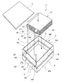
図1および図2において、電気二重層キャパシタ1は、ケース2、絶縁体10およびキャパシタ本体11を含んで構成されている。
1 and 2, the electric
ケース2は、第1,第2,第3,第4の側面部3,4,5,6および蓋部7,8を備えている。また、第1〜第4の側面部3,4,5,6は、2分割されており、第1の側面部3は一対の分割面部3A,3Bに分割され、第2の側面部4は一対の分割面部4A,4Bに分割されている。また、第3の側面部5は一対の分割面部5A,5Bに分割され、第4の側面部6は一対の分割面部6A,6Bに分割されている。なお、分割面部3A,4A,5A,6Aおよび蓋部7は、特許請求の範囲にいう「一方のケース」に相当し、分割面部3B,4B,5B,6Bおよび蓋部8は、特許請求の範囲にいう「他方のケース」に相当する。
The
ここで、第1の側面部3の分割面部3Aは、図3に示すように、上下方向に延び、その上端側が略L字状の切欠部3Eとなり、下端側は略L字状に4段階に屈曲した屈曲部3Cとなっている。第1の側面部3の分割面部3Bは、上下方向に延び、その上端側は略L字状に2段階に屈曲した屈曲部3Dとなっている。これら屈曲部3Cと屈曲部3D同士は、直接に接触せず、絶縁体10を介して接合している。
Here, as shown in FIG. 3, the dividing
上記屈曲部3Cは、第1の側面部3の分割面部3Aの下端側からケース2の内側方向へと水平方向に略L字状に屈曲した第1屈曲部3C1と、第1屈曲部3C1から下向きに略L字状に屈曲した第2屈曲部3C2と、第2屈曲部3C2からケース2の外側方向へと水平方向に屈曲した第3屈曲部3C3と、第3屈曲部3C3から上向きに略L字状に屈曲した第4屈曲部3C4とによって構成されている。
The
また上記屈曲部3Dは、分割面部3Bの上端側からケース2の内側方向へと水平方向に第1屈曲部3C1と第4屈曲部3C4との間に向けて略L字状に屈曲した第1屈曲部3D1と、第1屈曲部3D1から下向きに第2屈曲部3C2と第4屈曲部3C4との間に向けて略L字状に屈曲した第2屈曲部3D2とによって構成されている。また、第2〜第4の側面部4,5,6についても第1の側面部3と同様に構成され、切欠部および屈曲部(いずれも図示せず)を有している。
The
なお、本実施の形態では、第1の側面部3の分割面部3A,3Bに屈曲部3C,3Dを設け、第2〜第4の側面部4〜6についても第1の側面部3と同様に構成する場合を例に挙げて説明したが、これに替えてもよいその他の変形例として、以下のものを挙げることができる。
In the present embodiment,
第1の変形例を図4に示す。第1の変形例は、第1〜第4の側面部3〜6を、一方向にストレートに延びる分割面部300と、同じく他方向にストレートに延びる分割面部301とから構成し、これら分割面部300,301を絶縁体10によって接合する構成にするものである。
A first modification is shown in FIG. In the first modification, the first to fourth
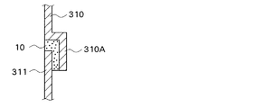
第2の変形例を図5に示す。第2の変形例は、第1〜第4の側面部3〜6を、一端側が略L字状に屈曲した屈曲部310Aを有する分割面部310と、一方向にストレートに延びる分割面部311とから構成し、これら分割面部310の屈曲部310Aと分割面部311を絶縁体10によって接合する構成にするものである。
A second modification is shown in FIG. In the second modification, the first to fourth
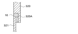
第3の変形例を図6に示す。第3の変形例は、第1〜第4の側面部3〜6を、一端側に略L字状に切り欠かれた切欠部320Aを有する分割面部320と、一方向にストレートに延びる分割面部321とから構成し、これら分割面部320の切欠部320Aと分割面部321を絶縁体10によって接合する構成にするものである。
A third modification is shown in FIG. In the third modification, the first to fourth
第4の変形例を図7に示す。第4の変形例は、第1〜第4の側面部3〜6を、一端側に略L字状に切り欠かれた切欠部330Aを有する分割面部330と、一端側に略L字状に切り欠かれた切欠部331Aを有する分割面部331とから構成し、これら分割面部330,331の切欠部330A,331Aを絶縁体10によって接合する構成にするものである。
A fourth modification is shown in FIG. In the fourth modified example, the first to fourth
屈曲部3C,3Dの変形例として第1〜第4の変形例を以上に説明したが、屈曲部3C,3Dの変形例は、ケース2の一方のケースと他方のケースを電気的に絶縁した状態で、ケース2を形成できる構造であればよく、これらに限定されるものではない。
The first to fourth modified examples have been described above as modified examples of the
また、前記第1の変形例で述べた分割面部300と分割面部301との対向面の形状においても以下の変形例を挙げることができる。
Moreover, the following modifications can be given also in the shape of the facing surfaces of the divided
第5の変形例を図8に示す。第5の変形例は、分割面部301と対向する分割面部300の対向面の少なくとも一部に断面略三角形状の突起300Bを突設すると共に、分割面部300と対向する分割面部301の対向面の少なくとも一部に断面略三角形状の突起301Bを突設するものである。
A fifth modification is shown in FIG. In the fifth modification, a
第6の変形例を図9に示す。第6の変形例は、分割面部301と対向する分割面部300の対向面の少なくとも一部に断面のこぎり刃状をなしたのこぎり刃300Cを形成すると共に、分割面部300と対向する分割面部301の対向面の少なくとも一部に断面のこぎり刃状をなしたのごきり刃301Cを形成するものである。
A sixth modification is shown in FIG. In the sixth modified example, a
第7の変形例を図10に示す。第7の変形例は、分割面部301と対向する分割面部300の対向面の少なくとも一部に断面略四角形状をなした複数の凸部300Dを突設すると共に、分割面部300と対向する分割面部301の対向面の少なくとも一部に断面略四角形状をなした複数の凸部301Dを突設するものである。
A seventh modification is shown in FIG. In the seventh modified example, a plurality of
第8の変形例を図11に示す。第8の変形例は、分割面部301と対向する分割面部300の対向面の少なくとも一部に断面凹湾曲状をなした複数の円弧部300Eを凹設すると共に、分割面部300と対向する分割面部301の対向面の少なくとも一部に断面凹湾曲状をなした複数の円弧部301Eを凹設するものである。
An eighth modification is shown in FIG. In the eighth modification, a plurality of
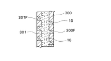
第9の変形例を図12に示す。第9の変形例は、分割面部301と対向する分割面部300の対向面の少なくとも一部に貫通孔300Fを穿設すると共に、分割面部300と対向する分割面部301の対向面の少なくとも一部に貫通孔301Fを穿設するものである。この場合、絶縁体10は貫通孔301F中の絶縁体10と一体化することで、強力なアンカー効果を期待できる。
A ninth modification is shown in FIG. In the ninth modification, a through
第10の変形例を図13に示す。第10の変形例は、分割面部301と対向する分割面部300の対向面の少なくとも一部を波形部300Gとして形成すると共に、分割面部300と対向する分割面部301の対向面の少なくとも一部を波形部301Gとして形成するものである。
A tenth modification is shown in FIG. In the tenth modification, at least a part of the facing surface of the
分割面部300と分割面部301との対向面の形状の変形例として第5〜第10の変形例を以上に説明したが、対向面の形状の変形例は、ケース2の一方のケースと他方のケースを、電気的に絶縁した状態で絶縁体10に対してアンカー効果を発現し、ケース2を形成できる構造であればよく、これらに限定されるものではない。
Although the fifth to tenth modification examples have been described above as the modification examples of the shape of the facing surfaces of the dividing
以上に述べた、これら第5〜第10の変形例における分割面部300,301の形状は、第2〜第4の変形例においても適用される。
The shapes of the dividing
そして、第1の側面部3の切欠部3Eおよび第2〜第4の側面部4,5,6の切欠部には蓋部7の外周側に形成された切欠部7Aが溶接等により嵌合して取り付けられている。また、第1〜第4の側面部3,4,5,6の下端側には蓋部8が一体形成されている。
And the
図1および図2に示すように略直方体状の箱体として形成されるケース2の材料としては、導電性材料である金属材料を用いる。ケース2の一方のケースがアルミニウムまたはアルミニウム合金からなることが好ましく、この一方のケースには正電極が接続されることがさらに好ましい。金属材料としてはその導電率が1×10⁻⁴Scm−1以上の金属が好ましく、ケース2の他方のケースは鉄、ニッケル、銅、クロム、アルミニウム、亜鉛、マグネシウム、マンガンのうちの1種類の金属材料または2種類以上からなる合金であることが好ましい。
As shown in FIGS. 1 and 2, a metal material that is a conductive material is used as the material of the
前記ケース2に用いるアルミニウム合金としては、アルミニウムの含有量が全重量の99%以上で、鉄、銅、マンガン、亜鉛、マグネシウム、クロム、ニッケル、ビスマス、鉛などが含まれるものである。具体的には2000系アルミニウム合金(Al−Cu−Mg系合金)、3000系アルミニウム合金(Al−Mn系合金)、4000系アルミニウム合金(Al−Si系合金)、6000系アルミニウム合金(Al−Mg−Si系合金)、7000系アルミニウム合金(Al−Zn−Mg系合金)、8000系アルミニウム合金(Al−Li系合金など)が挙げられる。アルミニウム合金に含まれるアルミニウム以外の元素は、JIS H 1306に準じて原子吸光法などで測定できる。
The aluminum alloy used for the
また、本発明で使用できる金属材料の導電率は、JIS C 2525に準じて測定される導体抵抗の逆数を求めることで特定できる。 Moreover, the electrical conductivity of the metal material which can be used by this invention can be specified by calculating | requiring the reciprocal number of the conductor resistance measured according to JISC2525.
絶縁体10は、図1および図2に示すように、長方形状の枠状体として形成され、第1の側面部3の分割面部3A,3Bの屈曲部3C,3D間に隙間なく溶着されている。また、この絶縁体10は、第2の側面部4の分割面部4A,4Bの屈曲部間、第3の側面部5の分割面部5A,5Bの屈曲部間、第4の側面部6の分割面部6A,6Bの屈曲部間にも隙間なく溶着されている。このため、分割面部3A,4A,5A,6Aと分割面部3B,4B,5B,6Bとは絶縁体10によって強固に固定されている。
As shown in FIGS. 1 and 2, the
そして、絶縁体10はケース2の6面のうち4面を横切ってケース2を取り囲むように形成されると共に、ケース2の12辺のうち4辺を横切って形成されている。また、絶縁体10は、その導電率が1×10⁻⁷Scm−1以下であることが好ましい。具体的には、熱硬化性樹脂、熱可塑性樹脂、ゴム、フッ素含有樹脂、無機酸化物から選ばれるものによって形成されることが好ましい。
The
熱硬化性樹脂としては、フェノール樹脂、不飽和ポリエステル、エポキシ樹脂、ポリイミドおよびこれらの混合物などが挙げられる。熱可塑性樹脂としては、ポリエチレンテレフタレート、ポリブチレンテレフタレートなどのポリエステル、ポリプロピレン、ポリカーボネート、アクリル樹脂、ポリ塩化ビニル、ポリアミド、ポリアミドイミド、ポリフェニレンサルファイドおよびこれらの混合物が挙げられる。ゴムとしてはエチレン−プロピレンゴム、ブチルゴム、アクリルゴム、クロロスルホン化ポリエチレンゴム、シリコーンゴム、フッ素ゴムおよびこれらの混合物が挙げられる。フッ素含有樹脂としてはポリテトラフルオロエチレン、テトラフルオロエチレン−ヘキサフルオロプロピレン共重合体、ポリフッ化ビニリデンおよびこれらの混合物が挙げられる。無機酸化物としては、石英ガラス、ソーダ石灰ガラスなどのガラスやセラミックが挙げられる。さらには、上記樹脂成分に上記無機酸化物からなる繊維状補強剤を混合した組成物を絶縁体としてもよい。 Examples of the thermosetting resin include phenol resin, unsaturated polyester, epoxy resin, polyimide, and a mixture thereof. Examples of the thermoplastic resin include polyesters such as polyethylene terephthalate and polybutylene terephthalate, polypropylene, polycarbonate, acrylic resin, polyvinyl chloride, polyamide, polyamideimide, polyphenylene sulfide, and mixtures thereof. Examples of the rubber include ethylene-propylene rubber, butyl rubber, acrylic rubber, chlorosulfonated polyethylene rubber, silicone rubber, fluororubber, and mixtures thereof. Examples of the fluorine-containing resin include polytetrafluoroethylene, tetrafluoroethylene-hexafluoropropylene copolymer, polyvinylidene fluoride, and mixtures thereof. Examples of the inorganic oxide include glass and ceramic such as quartz glass and soda lime glass. Furthermore, it is good also considering the composition which mixed the fibrous reinforcing agent which consists of the said inorganic oxide with the said resin component as an insulator.
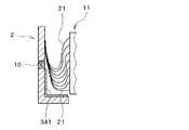
キャパシタ本体11は、図1に示すように、分極性電極である正電極20および分極性電極である負電極30が隔離板(図示せず)を介して交互に積層されて構成され、ケース2内に収容されている。そして、これら正電極20、負電極30および隔離板は、電解液が含浸されている状態でケース2内に収容される。
As shown in FIG. 1, the
各正電極20にはそれぞれ正極側端子21が溶着されており、これら正極側端子21は1つに束ねられてケース2を構成する第1の側面部3の分割面部3Aの内壁面に形成された接続部位22(図1中の2点鎖線参照)に電気的に接続されている。このため、ケース2のうち、分割面部3A,4A,5A,6Aおよび蓋部7は正極部となっている。
Each
各負電極30にはそれぞれ負極側端子31が溶着されており、これら負極側端子31は1つに束ねられてケース2を構成する第1の側面部3の分割面部3Bの内壁面に形成された接続部位32(図1中の2点鎖線参照)に電気的に接続されている。このため、分割面部3B,4B,5B,6Bおよび蓋部8は負極部となっている。
Each
なお、図1の1つに束ねられた正極側端子21を積層した電極の近傍まで曲げて、正極側端子21とケース2の内面との距離を小さくして、ケース2内のデッドスペースを極力小さくするときには、端子の接合部以外の撓めた部分がケース2の極性が異なる部分の内面に触れないように、端子とケース2の内面との間に距離を保つ工夫をする。例えば、端子の接合部以外の適宜箇所を絶縁体でできたリング、端部が開口した中空の筒、テープなどのフィルムで覆うか、ケース2の内面の端子が触れる箇所に絶縁体のフィルムを貼ればよい。図14に示す第11の変形例は、束ねた正極側端子21を絶縁体のリング340に通した例である。このようにすることで、端子とケース2の内面との間に距離を確実に保つことができる。図15に示す第12の変形例は、ケース2の内面の正極側端子21が触れる虞れのある位置に絶縁フィルム341を貼着した例である。
In addition, it bends to the vicinity of the electrode which laminated | stacked the positive
正極側端子21とケース2の内面との距離に、厚みのある溶接機などを差し込んで作業する余裕があるときは、束ねた正極側端子を、接合する側のケース2へ向けて屈曲させてケース2の内面に接合してもよい。このとき、2つの束ねた正極側端子21、負極側端子31の対向する面それぞれがケース2内に接合される。
If there is room to work by inserting a thick welder or the like in the distance between the
また、電極をケース内面へ接合方法するそのほかの方法としては、図16に示す第13の変形例のように、積層する正電極20の基板全てと負電極30の基板全てを電極の積層方向と直交して180度逆向きとなる異なる方向へ延長し、延長した基板の縁をそれぞれ導電性の平板351,352に溶接し、この導電性の平板351,352からタブ351A,352Aを引き出してケース2の内面に接合する方法もある。なお、正電極20と負電極30を例えば90度異なる方向へと延長してもよい。
Further, as another method of joining the electrodes to the inner surface of the case, as in the thirteenth modification shown in FIG. 16, all the substrates of the
ケース2に装着するその他の部材としては圧力調整弁40を挙げることができる。この圧力調整弁40は、ゴムなどの弾性体からなり、キャパシタ本体11が充電される際に発生した気体によりケース2の内部の圧力が上昇して所定の圧力に到達したときに押し上げられて開弁することによってケース2の内部の気体をケース2の外部に逃がし、所定の圧力以下になったときにその弾性により形状が復元して閉弁するようになっている。
Examples of other members attached to the
図2の圧力調整弁40は、ケース2の外側に、ケース2の外表面から突出しないように、即ちケース2の外表面とほぼ面一となるように配置している装着の一例である。図2において、圧力調整弁40はケース2の一方のケースに設けても、他方のケースに設けてもよい。
The
圧力調整弁40の装着の他の具体例としては、図17に示す第14の変形例が挙げられる。第14の変形例はケース2に中心部にケース2の内外を貫通する穴を穿設した凹み部360を設け、この凹み部360に上蓋361Aと下蓋361Bで取り囲まれた弁体361Cからなる圧力調整弁361自体をケース2の凹み部360にねじ込んで配置するものである。上蓋361Aの側方部あるいは上方部には、弁体361Cの側方と上蓋361A内側の隙間に通じる穴が貫通している。この圧力調整弁361を設ける場合、圧力調整弁361の動作を妨げないよう穴を開けた蓋(図示せず)をケース2の外平面に溶接するか、穴を開けた平板状のねじ(図示せず)で圧力調整弁361をケース2の凹み部360に固定してもよい。
As another specific example of mounting of the
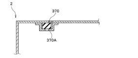
他の具体例として図18に示す第15の変形例も挙げることができる。第15の変形例のように、圧力調整弁370のケース2への装着はケース2の内面側であってもよい。この場合、ケース2には、弁体370Aの側方の隙間に通じる穴が貫通している。
As another specific example, a fifteenth modification shown in FIG. 18 can be given. As in the fifteenth modification, the
さらにケース2には電解液をケース2内に供給するための供給口50が穿設される。供給口50は、図1においてはケース2の第1の側面部3の分割面部3Bに穿設される。この供給口50は、電解液をケース2内に注入した後、電解液が外部に漏出しなければよく、分割面3Aに穿設してもよいし、他の分割面に穿設してもよい。図1においては、電解液を注入後、この供給口50に蓋板52を溶接してケース2を密閉する。この蓋板52は平板状のねじで、ケース2の表面とほぼ面一となるように、ケース2にねじ止めしてもよい。
Further, the
この供給口50は、例えば図19に示す第16の変形例のように、ケース2の外表面から突出しないように配置する弁体372の下部のケース2に穿設する穴と兼用していてもよい。このことは図17に示す第14の変形例でも同様である。
The
この第16の変形例の場合、供給口50から電解液を注入した後、供給口50の上に合わせて弁体372を載置し、ケース2の外部にガスを逃がす穴373を穿設した蓋374をケース2の外表面に溶接して、蓋374とケース2の凹み部360との間に弁体372を固定する。蓋374に穿設する穴373は、図18に示す第15の変形例と同様に、圧力調整弁として作用する弁体372の動作を妨げないように、弁体372の側方の隙間に通じていればよい。穴373を穿設した蓋374は、ケース2の外表面に溶接する他に、穴を穿設した平板状のねじとして、ケース2の凹み部360の開口部に、ケース2の外表面とほぼ面一となるようにねじ込んで配置してもよい。
In the case of the sixteenth modification, after injecting the electrolyte from the
以上、本実施の形態のケース2を用いた電気二重層キャパシタ1の構成を説明したが、製造工程としては、以下の手順が好ましい。
As mentioned above, although the structure of the electric
図17に示す圧力調整弁361を用いる場合、正極側端子21が溶着された正電極20および負極側端子31が溶着された負電極30を隔離板を介して交互に積層してキャパシタ本体11を形成する。他方で、蓋部7を除いたケース2を形成しておく。次に、各正極側端子21を1つに束ねて蓋部7を除いたケース2内部の接続部位22に接続すると共に、各負極側端子31も同様にして接続部位32に接続しつつ、キャパシタ本体11をケース2内に収容する。次に、蓋部7をケース2に取り付けた後、凹み部360の中心部に穿設した穴からケース2内に電解液を注入する。そして、最後に、圧力調整弁361をケース2の凹み部360に外側から装着する。
When the
また、図18または図19に示す前記圧力調整弁370(弁体372)を用いる場合には、まず、圧力調整弁370(弁体372)をケース2の内側から装着する。そして、キャパシタ本体11の各正極側端子21を1つに束ねてケース2の接続部位22に接続すると共に、各負極側端子31を1つに束ねてケース2の接続部位32に接続しつつ、キャパシタ本体11をケース2内に収容し蓋部7をケース2に取り付ける。そして、最後に、供給口50からケース2内に電解液を注入し、図18の場合は供給口50上に蓋板52を取り付け、図19の場合は、供給口50上に弁体372を配置し、蓋374を取り付けて弁体372を固定する。
When using the pressure regulating valve 370 (valve element 372) shown in FIG. 18 or FIG. 19, first, the pressure regulating valve 370 (valve element 372) is mounted from the inside of the
このように構成される電気二重層キャパシタ1によれば、ケース2を剛性の高い金属材料を用いて形成したので、電気二重層キャパシタ1を長時間使用した場合でも、従来技術のようなケース2におけるピンホール等の損傷が生じないようにする製造上の手間のかかる管理を行うこともなく、電気二重層キャパシタ1の寿命、耐久性等を高めることができる。
According to the electric
また、正電極20の正極側端子21および負電極30の負極側端子31をケース2の内壁面に接続する構成としたので、従来技術のようにこれら各端子をキャパシタ本体に突設させて形成する必要がなくなり、ケース2を含めた電気二重層キャパシタ1全体をコンパクトに形成することができる。
Further, since the positive
そして、本発明の電気二重層キャパシタは、直方体状に形成したので、これら複数個のキャパシタを用いて、一方のキャパシタの正極部と他方のキャパシタの負極部が接するように並べることで、直列型の電気二重層キャパシタ組立体(以下、キャパシタ組立体という)を構成することができる。あるいは、一方のキャパシタの正極部と他方のキャパシタの正極部、かつ一方のキャパシタの負極部と他方のキャパシタの負極部が接するように並べることで、並列型の電気二重層キャパシタ組立体を構成することができる。2つの電気二重層キャパシタ間の接合は、電気的に接続がなされるのであれば、溶接、圧接、導電性部材を介する接合など、その方法は限定されない。 And since the electric double layer capacitor of the present invention was formed in the shape of a rectangular parallelepiped, it was arranged in series so that the positive electrode part of one capacitor and the negative electrode part of the other capacitor were in contact with each other using these capacitors. The electric double layer capacitor assembly (hereinafter referred to as a capacitor assembly) can be configured. Alternatively, a parallel type electric double layer capacitor assembly is configured by arranging the positive electrode part of one capacitor and the positive electrode part of the other capacitor, and the negative electrode part of one capacitor and the negative electrode part of the other capacitor in contact with each other. be able to. As long as electrical connection is made between the two electric double layer capacitors, the method is not limited, such as welding, pressure welding, or joining via a conductive member.
一具体例として、本発明の第2の実施の形態に係る電気二重層キャパシタを図20を用いて説明する。なお、本実施の形態では、第1の実施の形態と同一の構成要素に同一の符号を付し、その説明を省略するものとする。
図20において、100は本実施の形態に係る電気二重層キャパシタ組立体を示し、このキャパシタ組立体100は、電気二重層キャパシタ1(以下、キャパシタ1という)のうち、正極部である蓋部7と負極部である蓋部8とが衝合(面接触)するように複数個(4個)直列に並べられて構成されている。そして、これらキャパシタ1のうち互いに隣接する蓋部7の周辺部同士と蓋部8の周辺部同士(図20中の×印参照)は、レーザ溶接またはシーム溶接を用いて溶接部41によって溶接されている。
As a specific example, an electric double layer capacitor according to a second embodiment of the present invention will be described with reference to FIG. In the present embodiment, the same components as those in the first embodiment are denoted by the same reference numerals, and the description thereof is omitted.
In FIG. 20,
このように構成される本実施の形態では、複数個のキャパシタ1を複数個直列に並べて蓋部7の周辺部と蓋部8の周辺部を溶接部41により接合するだけで、これら複数個のキャパシタ1を電気的に接続することができ、コンパクトでかつ大容量のキャパシタ組立体100を構成することができる。
In the present embodiment configured as described above, a plurality of
もうひとつの具体例として、本発明の第3の実施の形態に係る電気二重層キャパシタを図21を用いて説明する。 As another specific example, an electric double layer capacitor according to a third embodiment of the present invention will be described with reference to FIG.
図21において、200は本実施の形態に係る電気二重層キャパシタ組立体(以下、キャパシタ組立体という)を示し、このキャパシタ組立体200は、複数個(4個)の電気二重層キャパシタ201(以下、キャパシタ201という)によって構成されている。
In FIG. 21,
キャパシタ201はケース202を有し、このケース202は、第1,第2,第3,第4の側面部203,204,205,206、蓋部207,208および絶縁体209を備えている。そして、ケース202のうち、分割面部203A,204A,205A,206Aおよび蓋部207は正極部となっている。また、ケース202のうち、分割面部203B,204B,205B,206Bおよび蓋部208は負極部となっている。
The
そして、キャパシタ201は、一方のキャパシタ201の正極部である分割面部206A、蓋部207と他方のキャパシタ201の正極部である分割面部206A、蓋部207とがそれぞれ接し、かつ一方のキャパシタ201の負極部である分割面部206Bと他方のキャパシタ201の負極部である分割面部206Bとが接するように複数個並列に並べられている。そして、これらキャパシタ201のうち互いに隣接する分割面部206Aの周辺部同士、分割面部206Bの周辺部同士、蓋部207の周辺部同士(図21中の×印参照)は、レーザ溶接またはシーム溶接を用いて溶接部51によって溶接されている。
このように構成される本実施の形態でも、複数個のキャパシタ201を複数個並列に並べてこれらキャパシタ201を溶接部51により接合するだけで、複数個のキャパシタ201を電気的に接続することができ、コンパクトでかつ大容量のキャパシタ組立体200を構成することができる。
Also in this embodiment configured as described above, a plurality of
なお、第1の実施の形態では、絶縁体10がケース2の6面のうち4面を横切るように形成する場合を例に挙げて説明したが、本発明はこれに限らず、例えば図22に示す本発明の第17の変形例のように絶縁体60を、ケース2の3面を横切るように配置してもよい。
In the first embodiment, the case where the
また、第1の実施の形態では、絶縁体10がケース2の12辺のうち4辺を横切るように形成する場合を例に挙げて説明したが、本発明はこれに限らず、例えば図23に示す本発明の第18の変形例のように、絶縁体70をケース2の6辺に沿って延びるように形成してもよい。
Further, in the first embodiment, the case where the
1,201 電気二重層キャパシタ、2,202 ケース、10,60,70,209 絶縁体、20 正電極、30 負電極、100,200 電気二重層キャパシタ組立体。 1,201 electric double layer capacitor, 2,202 case, 10, 60, 70, 209 insulator, 20 positive electrode, 30 negative electrode, 100, 200 electric double layer capacitor assembly.
Claims (9)
前記一対の電極と隔離板と電解液とを収納するケースが導電性材料によって形成され、該ケースは一方のケースと他方のケースとに二分割され、これら一方のケースと他方のケースとの境界部に沿って絶縁体を配設することにより前記絶縁体で前記一方のケースと他方のケースとを固定し、前記一方のケースには前記一対の電極のうち正電極が接続され、前記他方のケースには前記一対の電極のうち負電極が接続されたことを特徴とする電気二重層キャパシタ。 An electric double layer capacitor comprising a pair of electrodes, at least one of which is a polarizable electrode, a separator and an electrolyte,
A case for housing the pair of electrodes, the separator, and the electrolyte is formed of a conductive material, and the case is divided into one case and the other case, and a boundary between the one case and the other case The one case and the other case are fixed by the insulator by disposing an insulator along the portion, and the positive electrode of the pair of electrodes is connected to the one case, and the other case An electric double layer capacitor, wherein a negative electrode of the pair of electrodes is connected to the case.
1×10⁻⁴Scm−1以上であることを特徴とする請求項1または2に記載の電気二重層キャパシタ。 The metal material of the other case is an alloy composed of one or more of iron, nickel, copper, chromium, aluminum, zinc, magnesium, and manganese, and the conductivity is 1 × 10 −4 Scm −1. It is the above, The electric double layer capacitor of Claim 1 or 2 characterized by the above-mentioned.
Of the plurality of electric double layer capacitors according to claim 2, the positive electrode part of one capacitor and the positive electrode part of the other capacitor are arranged so that the negative electrode part of one capacitor and the negative electrode part of the other capacitor are in contact with each other. A parallel type electric double layer capacitor characterized by the above.
Priority Applications (5)
| Application Number | Priority Date | Filing Date | Title |
|---|---|---|---|
| JP2006115906A JP2007288059A (en) | 2006-04-19 | 2006-04-19 | Electric double layer capacitor |
| CNA2007800135789A CN101421804A (en) | 2006-04-19 | 2007-04-11 | Electric double layer capacitor |
| EP07741411A EP2009655A1 (en) | 2006-04-19 | 2007-04-11 | Electric double layer capacitor |
| PCT/JP2007/057975 WO2007123033A1 (en) | 2006-04-19 | 2007-04-11 | Electric double layer capacitor |
| US12/224,675 US20090027829A1 (en) | 2006-04-19 | 2007-04-11 | Electric Double Layer Capacitor |
Applications Claiming Priority (1)
| Application Number | Priority Date | Filing Date | Title |
|---|---|---|---|
| JP2006115906A JP2007288059A (en) | 2006-04-19 | 2006-04-19 | Electric double layer capacitor |
Publications (1)
| Publication Number | Publication Date |
|---|---|
| JP2007288059A true JP2007288059A (en) | 2007-11-01 |
Family
ID=38624938
Family Applications (1)
| Application Number | Title | Priority Date | Filing Date |
|---|---|---|---|
| JP2006115906A Pending JP2007288059A (en) | 2006-04-19 | 2006-04-19 | Electric double layer capacitor |
Country Status (5)
| Country | Link |
|---|---|
| US (1) | US20090027829A1 (en) |
| EP (1) | EP2009655A1 (en) |
| JP (1) | JP2007288059A (en) |
| CN (1) | CN101421804A (en) |
| WO (1) | WO2007123033A1 (en) |
Cited By (3)
| Publication number | Priority date | Publication date | Assignee | Title |
|---|---|---|---|---|
| JP2012079833A (en) * | 2010-09-30 | 2012-04-19 | Ibiden Co Ltd | Power storage package structure, electrochemical device, and electrochemical module |
| KR101244280B1 (en) | 2011-08-08 | 2013-03-18 | 비나텍주식회사 | Super capacitor having case terminal |
| JP2013089904A (en) * | 2011-10-21 | 2013-05-13 | Nec Tokin Corp | Electric double layer capacitor |
Families Citing this family (2)
| Publication number | Priority date | Publication date | Assignee | Title |
|---|---|---|---|---|
| KR20130034411A (en) * | 2011-09-28 | 2013-04-05 | 삼성전기주식회사 | Energy storage module |
| CN115779202A (en) * | 2021-09-10 | 2023-03-14 | 深圳摩尔雾化健康医疗科技有限公司 | Aerosol generating device |
Citations (3)
| Publication number | Priority date | Publication date | Assignee | Title |
|---|---|---|---|---|
| JPH1154388A (en) * | 1997-07-30 | 1999-02-26 | Honda Motor Co Ltd | Electric double-layer capacitor |
| JP2001502117A (en) * | 1996-10-07 | 2001-02-13 | マックスウェル テクノロジーズ インコーポレイテッド | Multi-electrode double-layer capacitor |
| JP2005183373A (en) * | 2003-11-27 | 2005-07-07 | Kyocera Corp | Battery case, manufacturing method thereof and battery, electric double-layer capacitor case and manufacturing method thereof, and electric double-layer capacitor |
Family Cites Families (7)
| Publication number | Priority date | Publication date | Assignee | Title |
|---|---|---|---|---|
| JPH08138978A (en) * | 1994-11-02 | 1996-05-31 | Japan Gore Tex Inc | Electric double layer capacitor and manufacture of its electrode |
| US5850331A (en) * | 1996-08-30 | 1998-12-15 | Honda Giken Kogyo Kabushiki Kaisha | Electric double-layer capacitor and capacitor device |
| JP3796381B2 (en) * | 1999-01-26 | 2006-07-12 | 株式会社エスアイアイ・マイクロパーツ | Electric double layer capacitor |
| JP4018880B2 (en) | 2001-03-26 | 2007-12-05 | 日産ディーゼル工業株式会社 | Electric double layer capacitor and manufacturing method thereof |
| US20070139862A1 (en) * | 2003-10-09 | 2007-06-21 | Kaneka Corporation | Electrode composite body, electrolyte, and redox capacitor |
| CN1788325A (en) * | 2004-03-09 | 2006-06-14 | 三洋电机株式会社 | Electric double-layer capacitor |
| US7651813B2 (en) * | 2004-11-25 | 2010-01-26 | Kyocera Corporation | Container, battery and electric double layer capacitor |
-
2006
- 2006-04-19 JP JP2006115906A patent/JP2007288059A/en active Pending
-
2007
- 2007-04-11 EP EP07741411A patent/EP2009655A1/en not_active Withdrawn
- 2007-04-11 US US12/224,675 patent/US20090027829A1/en not_active Abandoned
- 2007-04-11 CN CNA2007800135789A patent/CN101421804A/en active Pending
- 2007-04-11 WO PCT/JP2007/057975 patent/WO2007123033A1/en active Application Filing
Patent Citations (3)
| Publication number | Priority date | Publication date | Assignee | Title |
|---|---|---|---|---|
| JP2001502117A (en) * | 1996-10-07 | 2001-02-13 | マックスウェル テクノロジーズ インコーポレイテッド | Multi-electrode double-layer capacitor |
| JPH1154388A (en) * | 1997-07-30 | 1999-02-26 | Honda Motor Co Ltd | Electric double-layer capacitor |
| JP2005183373A (en) * | 2003-11-27 | 2005-07-07 | Kyocera Corp | Battery case, manufacturing method thereof and battery, electric double-layer capacitor case and manufacturing method thereof, and electric double-layer capacitor |
Cited By (3)
| Publication number | Priority date | Publication date | Assignee | Title |
|---|---|---|---|---|
| JP2012079833A (en) * | 2010-09-30 | 2012-04-19 | Ibiden Co Ltd | Power storage package structure, electrochemical device, and electrochemical module |
| KR101244280B1 (en) | 2011-08-08 | 2013-03-18 | 비나텍주식회사 | Super capacitor having case terminal |
| JP2013089904A (en) * | 2011-10-21 | 2013-05-13 | Nec Tokin Corp | Electric double layer capacitor |
Also Published As
| Publication number | Publication date |
|---|---|
| US20090027829A1 (en) | 2009-01-29 |
| CN101421804A (en) | 2009-04-29 |
| EP2009655A1 (en) | 2008-12-31 |
| WO2007123033A1 (en) | 2007-11-01 |
Similar Documents
| Publication | Publication Date | Title |
|---|---|---|
| CN207800665U (en) | The cap assembly and secondary cell of secondary cell | |
| JP5317129B2 (en) | Secondary battery | |
| JP4158518B2 (en) | Electricity storage element | |
| KR20120075401A (en) | Storage element | |
| JP6178418B2 (en) | Battery cell with current collector in contact with housing | |
| JP2011014859A (en) | Electric double layer capacitor | |
| JP2014160618A (en) | Storage element | |
| JP2003045760A (en) | Laminated electric double-layer capacitor module | |
| JP2007288059A (en) | Electric double layer capacitor | |
| JP2015185470A (en) | Power storage element | |
| JP4032958B2 (en) | Storage element and method for manufacturing the same | |
| JP6015582B2 (en) | Electricity storage element | |
| JP6414577B2 (en) | Stacked battery | |
| JP2010225372A (en) | Battery, vehicle, and battery-mounting equipment | |
| JP6187148B2 (en) | Storage element and power supply module | |
| JP2020149952A (en) | Power storage element | |
| JP6295695B2 (en) | Storage element and power supply module | |
| JP6645533B2 (en) | Storage element | |
| JP2015035303A (en) | Terminal structure | |
| JP2015022941A (en) | Power storage element | |
| JP2003059783A (en) | Electric double layer capacitor | |
| JP2015088372A (en) | Terminal structure | |
| JP2020107463A (en) | Power storage device | |
| WO2023243548A1 (en) | Power storage element and production method for power storage element | |
| JP6502609B2 (en) | Storage element |
Legal Events
| Date | Code | Title | Description |
|---|---|---|---|
| A621 | Written request for application examination |
Free format text: JAPANESE INTERMEDIATE CODE: A621 Effective date: 20090126 |
|
| A131 | Notification of reasons for refusal |
Free format text: JAPANESE INTERMEDIATE CODE: A131 Effective date: 20110222 |
|
| A02 | Decision of refusal |
Free format text: JAPANESE INTERMEDIATE CODE: A02 Effective date: 20110705 |