JP2007266160A - Organic light emitting element array - Google Patents
Organic light emitting element array Download PDFInfo
- Publication number
- JP2007266160A JP2007266160A JP2006087015A JP2006087015A JP2007266160A JP 2007266160 A JP2007266160 A JP 2007266160A JP 2006087015 A JP2006087015 A JP 2006087015A JP 2006087015 A JP2006087015 A JP 2006087015A JP 2007266160 A JP2007266160 A JP 2007266160A
- Authority
- JP
- Japan
- Prior art keywords
- light emitting
- organic light
- layer
- transport layer
- emitting element
- Prior art date
- Legal status (The legal status is an assumption and is not a legal conclusion. Google has not performed a legal analysis and makes no representation as to the accuracy of the status listed.)
- Pending
Links
- 239000000463 material Substances 0.000 claims abstract description 43
- 230000005525 hole transport Effects 0.000 claims abstract description 28
- 239000003086 colorant Substances 0.000 abstract description 13
- 238000002347 injection Methods 0.000 description 10
- 239000007924 injection Substances 0.000 description 10
- 150000001875 compounds Chemical class 0.000 description 9
- 239000000758 substrate Substances 0.000 description 9
- 150000002894 organic compounds Chemical group 0.000 description 8
- 238000010586 diagram Methods 0.000 description 6
- 238000002360 preparation method Methods 0.000 description 6
- 239000010408 film Substances 0.000 description 5
- XKRFYHLGVUSROY-UHFFFAOYSA-N Argon Chemical compound [Ar] XKRFYHLGVUSROY-UHFFFAOYSA-N 0.000 description 4
- 238000005259 measurement Methods 0.000 description 4
- 238000000034 method Methods 0.000 description 4
- 238000004544 sputter deposition Methods 0.000 description 4
- 238000007740 vapor deposition Methods 0.000 description 4
- 238000000151 deposition Methods 0.000 description 3
- 239000011521 glass Substances 0.000 description 3
- 239000011159 matrix material Substances 0.000 description 3
- QFLWZFQWSBQYPS-AWRAUJHKSA-N (3S)-3-[[(2S)-2-[[(2S)-2-[5-[(3aS,6aR)-2-oxo-1,3,3a,4,6,6a-hexahydrothieno[3,4-d]imidazol-4-yl]pentanoylamino]-3-methylbutanoyl]amino]-3-(4-hydroxyphenyl)propanoyl]amino]-4-[1-bis(4-chlorophenoxy)phosphorylbutylamino]-4-oxobutanoic acid Chemical compound CCCC(NC(=O)[C@H](CC(O)=O)NC(=O)[C@H](Cc1ccc(O)cc1)NC(=O)[C@@H](NC(=O)CCCCC1SC[C@@H]2NC(=O)N[C@H]12)C(C)C)P(=O)(Oc1ccc(Cl)cc1)Oc1ccc(Cl)cc1 QFLWZFQWSBQYPS-AWRAUJHKSA-N 0.000 description 2
- XLOMVQKBTHCTTD-UHFFFAOYSA-N Zinc monoxide Chemical compound [Zn]=O XLOMVQKBTHCTTD-UHFFFAOYSA-N 0.000 description 2
- 238000000862 absorption spectrum Methods 0.000 description 2
- 239000003513 alkali Substances 0.000 description 2
- 229910052786 argon Inorganic materials 0.000 description 2
- QVGXLLKOCUKJST-UHFFFAOYSA-N atomic oxygen Chemical compound [O] QVGXLLKOCUKJST-UHFFFAOYSA-N 0.000 description 2
- 230000000903 blocking effect Effects 0.000 description 2
- 229910052792 caesium Inorganic materials 0.000 description 2
- TVFDJXOCXUVLDH-UHFFFAOYSA-N caesium atom Chemical compound [Cs] TVFDJXOCXUVLDH-UHFFFAOYSA-N 0.000 description 2
- 230000000052 comparative effect Effects 0.000 description 2
- 229940125782 compound 2 Drugs 0.000 description 2
- 230000008021 deposition Effects 0.000 description 2
- 239000007789 gas Substances 0.000 description 2
- 238000004770 highest occupied molecular orbital Methods 0.000 description 2
- 238000003384 imaging method Methods 0.000 description 2
- 238000004768 lowest unoccupied molecular orbital Methods 0.000 description 2
- 229910052751 metal Inorganic materials 0.000 description 2
- 239000002184 metal Substances 0.000 description 2
- 239000001301 oxygen Substances 0.000 description 2
- 229910052760 oxygen Inorganic materials 0.000 description 2
- 238000004402 ultra-violet photoelectron spectroscopy Methods 0.000 description 2
- GHYOCDFICYLMRF-UTIIJYGPSA-N (2S,3R)-N-[(2S)-3-(cyclopenten-1-yl)-1-[(2R)-2-methyloxiran-2-yl]-1-oxopropan-2-yl]-3-hydroxy-3-(4-methoxyphenyl)-2-[[(2S)-2-[(2-morpholin-4-ylacetyl)amino]propanoyl]amino]propanamide Chemical compound C1(=CCCC1)C[C@@H](C(=O)[C@@]1(OC1)C)NC([C@H]([C@@H](C1=CC=C(C=C1)OC)O)NC([C@H](C)NC(CN1CCOCC1)=O)=O)=O GHYOCDFICYLMRF-UTIIJYGPSA-N 0.000 description 1
- 238000010521 absorption reaction Methods 0.000 description 1
- 230000015572 biosynthetic process Effects 0.000 description 1
- 238000006243 chemical reaction Methods 0.000 description 1
- 229940125904 compound 1 Drugs 0.000 description 1
- 229940125773 compound 10 Drugs 0.000 description 1
- 229940125797 compound 12 Drugs 0.000 description 1
- 229940126214 compound 3 Drugs 0.000 description 1
- 229940125898 compound 5 Drugs 0.000 description 1
- 125000004122 cyclic group Chemical group 0.000 description 1
- 238000002484 cyclic voltammetry Methods 0.000 description 1
- 239000002019 doping agent Substances 0.000 description 1
- 230000003503 early effect Effects 0.000 description 1
- 238000005401 electroluminescence Methods 0.000 description 1
- 238000000605 extraction Methods 0.000 description 1
- 230000009477 glass transition Effects 0.000 description 1
- 239000012535 impurity Substances 0.000 description 1
- 229910003437 indium oxide Inorganic materials 0.000 description 1
- PJXISJQVUVHSOJ-UHFFFAOYSA-N indium(iii) oxide Chemical compound [O-2].[O-2].[O-2].[In+3].[In+3] PJXISJQVUVHSOJ-UHFFFAOYSA-N 0.000 description 1
- AMGQUBHHOARCQH-UHFFFAOYSA-N indium;oxotin Chemical compound [In].[Sn]=O AMGQUBHHOARCQH-UHFFFAOYSA-N 0.000 description 1
- ZLVXBBHTMQJRSX-VMGNSXQWSA-N jdtic Chemical compound C1([C@]2(C)CCN(C[C@@H]2C)C[C@H](C(C)C)NC(=O)[C@@H]2NCC3=CC(O)=CC=C3C2)=CC=CC(O)=C1 ZLVXBBHTMQJRSX-VMGNSXQWSA-N 0.000 description 1
- 238000010030 laminating Methods 0.000 description 1
- 230000031700 light absorption Effects 0.000 description 1
- 230000007774 longterm Effects 0.000 description 1
- 238000004519 manufacturing process Methods 0.000 description 1
- 230000003647 oxidation Effects 0.000 description 1
- 238000007254 oxidation reaction Methods 0.000 description 1
- 229910021420 polycrystalline silicon Inorganic materials 0.000 description 1
- 229920005591 polysilicon Polymers 0.000 description 1
- 239000011347 resin Substances 0.000 description 1
- 229920005989 resin Polymers 0.000 description 1
- 239000010409 thin film Substances 0.000 description 1
- 238000001771 vacuum deposition Methods 0.000 description 1
- 239000011787 zinc oxide Substances 0.000 description 1
Images

Classifications
-
- C—CHEMISTRY; METALLURGY
- C09—DYES; PAINTS; POLISHES; NATURAL RESINS; ADHESIVES; COMPOSITIONS NOT OTHERWISE PROVIDED FOR; APPLICATIONS OF MATERIALS NOT OTHERWISE PROVIDED FOR
- C09K—MATERIALS FOR MISCELLANEOUS APPLICATIONS, NOT PROVIDED FOR ELSEWHERE
- C09K11/00—Luminescent, e.g. electroluminescent, chemiluminescent materials
- C09K11/06—Luminescent, e.g. electroluminescent, chemiluminescent materials containing organic luminescent materials
-
- H—ELECTRICITY
- H10—SEMICONDUCTOR DEVICES; ELECTRIC SOLID-STATE DEVICES NOT OTHERWISE PROVIDED FOR
- H10K—ORGANIC ELECTRIC SOLID-STATE DEVICES
- H10K50/00—Organic light-emitting devices
- H10K50/10—OLEDs or polymer light-emitting diodes [PLED]
- H10K50/11—OLEDs or polymer light-emitting diodes [PLED] characterised by the electroluminescent [EL] layers
-
- H—ELECTRICITY
- H10—SEMICONDUCTOR DEVICES; ELECTRIC SOLID-STATE DEVICES NOT OTHERWISE PROVIDED FOR
- H10K—ORGANIC ELECTRIC SOLID-STATE DEVICES
- H10K50/00—Organic light-emitting devices
- H10K50/10—OLEDs or polymer light-emitting diodes [PLED]
- H10K50/14—Carrier transporting layers
-
- H—ELECTRICITY
- H10—SEMICONDUCTOR DEVICES; ELECTRIC SOLID-STATE DEVICES NOT OTHERWISE PROVIDED FOR
- H10K—ORGANIC ELECTRIC SOLID-STATE DEVICES
- H10K59/00—Integrated devices, or assemblies of multiple devices, comprising at least one organic light-emitting element covered by group H10K50/00
- H10K59/30—Devices specially adapted for multicolour light emission
- H10K59/35—Devices specially adapted for multicolour light emission comprising red-green-blue [RGB] subpixels
-
- C—CHEMISTRY; METALLURGY
- C09—DYES; PAINTS; POLISHES; NATURAL RESINS; ADHESIVES; COMPOSITIONS NOT OTHERWISE PROVIDED FOR; APPLICATIONS OF MATERIALS NOT OTHERWISE PROVIDED FOR
- C09K—MATERIALS FOR MISCELLANEOUS APPLICATIONS, NOT PROVIDED FOR ELSEWHERE
- C09K2211/00—Chemical nature of organic luminescent or tenebrescent compounds
- C09K2211/10—Non-macromolecular compounds
- C09K2211/1018—Heterocyclic compounds
- C09K2211/1025—Heterocyclic compounds characterised by ligands
- C09K2211/1044—Heterocyclic compounds characterised by ligands containing two nitrogen atoms as heteroatoms
-
- C—CHEMISTRY; METALLURGY
- C09—DYES; PAINTS; POLISHES; NATURAL RESINS; ADHESIVES; COMPOSITIONS NOT OTHERWISE PROVIDED FOR; APPLICATIONS OF MATERIALS NOT OTHERWISE PROVIDED FOR
- C09K—MATERIALS FOR MISCELLANEOUS APPLICATIONS, NOT PROVIDED FOR ELSEWHERE
- C09K2211/00—Chemical nature of organic luminescent or tenebrescent compounds
- C09K2211/18—Metal complexes
- C09K2211/185—Metal complexes of the platinum group, i.e. Os, Ir, Pt, Ru, Rh or Pd
-
- H—ELECTRICITY
- H10—SEMICONDUCTOR DEVICES; ELECTRIC SOLID-STATE DEVICES NOT OTHERWISE PROVIDED FOR
- H10K—ORGANIC ELECTRIC SOLID-STATE DEVICES
- H10K59/00—Integrated devices, or assemblies of multiple devices, comprising at least one organic light-emitting element covered by group H10K50/00
- H10K59/10—OLED displays
- H10K59/12—Active-matrix OLED [AMOLED] displays
Abstract
Description
本発明は有機EL(有機エレクトロルミネッセンス)素子を各色発光ごとに有する有機発光素子アレイに関する。より具体的にはフルカラー表示可能な表示装置等に用いられる有機発光素子アレイに関する。 The present invention relates to an organic light emitting element array having an organic EL (organic electroluminescence) element for each color emission. More specifically, the present invention relates to an organic light emitting element array used in a display device capable of full color display.
有機EL素子の研究が盛んである。そしてその発光非発光の制御にアクティブマトリクス駆動が用いられている。特許文献1には電源電極、有機EL素子、有機EL素子の発光非発光を制御するTFTが記載されている。
特許文献1は電流制御型発光素子に印加する電圧を低下し、低消費電力化を図ることを目的としている。そしてこれまでの課題はこのように発光素子に印加する電圧を低下させることで低消費電力化をはかるものであった。一方で本発明者は電源の電圧を上げないことに注目した。電源の電圧を上げない(高く設定しない)ということも低消費電力化を図るという意味で重要である。 Patent Document 1 aims to reduce the voltage applied to the current-controlled light-emitting element and reduce power consumption. The problem so far has been to reduce the power consumption by reducing the voltage applied to the light emitting element. On the other hand, the present inventor has paid attention to not increasing the voltage of the power source. Not increasing the voltage of the power supply (not setting it high) is also important in terms of reducing power consumption.
そこで本発明者は鋭意検討した。その際次のことに気が付いた。即ち電源の電圧を上げない(高く設定しない)ためには、各色の発光素子の駆動電圧を出来るだけ同じ電圧にそろえることが重要である。 Therefore, the present inventor has intensively studied. I noticed the following: That is, in order not to raise the voltage of the power supply (not set it high), it is important to set the driving voltages of the light emitting elements of the respective colors to the same voltage as much as possible.
本発明は各色の発光素子の駆動電圧が出来るだけ同じ電圧にそろった有機発光素子アレイを提供することを目的とする。 An object of the present invention is to provide an organic light emitting element array in which the driving voltages of the light emitting elements of the respective colors are set to the same voltage as much as possible.
よって本発明は、
有機発光層と前記有機発光層を間に配置する一対の電極とを有する有機発光素子と、前記有機発光素子の発光非発光を制御するトランジスタとを有し、
前記有機発光素子と前記トランジスタを赤及び緑及び青を発光するために各色毎に有する有機発光素子アレイにおいて、
前記有機発光層に接する正孔輸送層と、
前記有機発光層に接する電子輸送層と、を有し、
前記有機発光層はホスト材料とゲスト材料を有し、
前記正孔輸送層のイオン化ポテンシャルと全ての有機発光素子の前記有機発光層のホスト材料のイオン化ポテンシャルの差が0.2eV以下であり、
前記電子輸送層の電子親和力と全ての有機発光素子の前記有機発光層のホスト材料の電子親和力の差が0.2eV以下であることを特徴とする有機発光素子アレイを提供する。
Therefore, the present invention
An organic light emitting device having an organic light emitting layer and a pair of electrodes disposed between the organic light emitting layers, and a transistor for controlling light emission non-emission of the organic light emitting device,
In the organic light emitting element array having the organic light emitting element and the transistor for each color in order to emit red, green and blue,
A hole transport layer in contact with the organic light emitting layer;
An electron transport layer in contact with the organic light emitting layer,
The organic light emitting layer has a host material and a guest material,
The difference between the ionization potential of the hole transport layer and the ionization potential of the host material of the organic light emitting layer of all organic light emitting devices is 0.2 eV or less,
There is provided an organic light emitting device array, wherein a difference between an electron affinity of the electron transport layer and an electron affinity of a host material of the organic light emitting layer of all organic light emitting devices is 0.2 eV or less.
本発明の有機発光素子アレイは、各色の発光素子の駆動電圧を出来るだけ同じ電圧にそろえることが出来るので(各素子間の電位差は1V以内)、電源電圧を高く設定する必要が無くなる。 In the organic light-emitting element array of the present invention, the drive voltages of the light-emitting elements of the respective colors can be set to the same voltage as much as possible (the potential difference between the elements is within 1 V), so that it is not necessary to set the power supply voltage high.
本発明に係る有機発光素子アレイは、RGB(赤緑青)それぞれ発光する素子と、それぞれの発光素子の発光非発光を制御するためのトランジスタとを有している。また陽極および陰極の間に配置される有機発光層はホスト材料とゲスト材料とから少なくとも構成されている。また前記正孔輸送層のイオン化ポテンシャルと全ての有機発光素子の前記有機発光層のホスト材料のイオン化ポテンシャルの差が0.2eV以下である。 The organic light-emitting element array according to the present invention includes elements that emit light of RGB (red, green, and blue), and transistors that control light emission and non-light emission of each light-emitting element. The organic light emitting layer disposed between the anode and the cathode is composed of at least a host material and a guest material. The difference between the ionization potential of the hole transport layer and the ionization potential of the host material of the organic light emitting layer of all organic light emitting devices is 0.2 eV or less.
そして前記電子輸送層の電子親和力と全ての有機発光素子の前記有機発光層のホスト材料の電子親和力の差が0.2eV以下である。本実施形態に係る有機発光素子アレイはこのような構成を特徴とする有機発光素子アレイである。 And the difference of the electron affinity of the said electron carrying layer and the electron affinity of the host material of the said organic light emitting layer of all the organic light emitting elements is 0.2 eV or less. The organic light emitting element array according to the present embodiment is an organic light emitting element array characterized by such a configuration.
これによれば電源電圧を高く設定する必要が無くなる。その結果特に小型である携帯用表示装置の表示部として有機発光素子アレイを利用することも出来る。 This eliminates the need to set the power supply voltage high. As a result, the organic light-emitting element array can be used as a display unit of a portable display device that is particularly small.
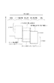
図1は本実施形態に係る有機発光素子アレイの有機発光素子におけるエネルギーダイアグラムを示す図である。有機発光層のホスト材料のイオン化ポテンシャルの差と有機発光層のホスト材料の電子親和力の差をそれぞれ図中に矢印で示した。 FIG. 1 is a diagram showing an energy diagram in an organic light emitting device of the organic light emitting device array according to the present embodiment. The difference in the ionization potential of the host material of the organic light emitting layer and the difference in the electron affinity of the host material of the organic light emitting layer are indicated by arrows in the figure.
有機発光素子から発光される互いに異なる色の光は、それぞれ有機発光素子とトランジスタ(例えばTFT)とから構成される最小単位から発する。 The light of different colors emitted from the organic light emitting element is emitted from the minimum unit composed of the organic light emitting element and a transistor (for example, TFT).
この最小単位における電位は、電源電位(Vcc)と接地電位(CGND)の差でその値が決められる。 The potential in this minimum unit is determined by the difference between the power supply potential (Vcc) and the ground potential (CGND).
また電源電位の値は、全素子において対向する一対の電極のうち一方の電極(例えば上部電極)が共通である場合同じ値である。 The value of the power supply potential is the same when one electrode (for example, the upper electrode) of a pair of electrodes facing each other is common.
また各最小単位のそれぞれが有するトランジスタは、有機発光素子アレイを作成するにあたり同一面内に同一の特性となるように作成されている。即ち発光色の違いによって特性は異なることが無いように作成されている。 Further, the transistors included in each minimum unit are formed so as to have the same characteristics in the same plane when the organic light emitting element array is formed. That is, it is created so that the characteristic does not differ depending on the difference in emission color.
つまり発光色毎に設けられる最小単位のそれぞれにおいて、電源電位は同じ電位であり、また接地電位も同じ電位であり、そしてトランジスタの特性は同一である。 That is, in each of the minimum units provided for each emission color, the power supply potential is the same potential, the ground potential is the same potential, and the transistor characteristics are the same.
そして本実施形態に係る有機発光素子アレイにおいて、発光色毎に設けられている有機発光素子の駆動電位が互いに1V以内でそろえている。 In the organic light emitting element array according to this embodiment, the driving potentials of the organic light emitting elements provided for the respective emission colors are aligned within 1V.
これまでの有機発光素子アレイは、発光色毎に設けられる最小単位のそれぞれにおいて、電源電位は同じ電位であり、また接地電位も同じ電位であり、そしてトランジスタの特性は同一であっても発光色毎に駆動電位が1V以上異なっていた。 In the conventional organic light emitting element array, the power supply potential is the same potential and the ground potential is the same potential in each of the minimum units provided for each emission color, and even if the transistor characteristics are the same, the emission color is the same. The driving potential was different by 1 V or more every time.
その場合一番駆動電位が高い素子を基準にトランジスタの特性を決める必要がある。より具体的に説明する。 In that case, it is necessary to determine the characteristics of the transistor based on the element having the highest driving potential. This will be described more specifically.
最小単位におけるトランジスタのソースドレイン電位をVsdとし、有機発光素子の駆動電位をVfとすると、次の式が成り立つ。
Vcc−CGND=Vf+Vsd=const.
有機発光素子の駆動電位Vfが高い場合Vsdは低くなる。その場合Vsdが低くなりすぎるとトランジスタのV−I特性から所望の電流をトランジスタが流すことが出来なくなる。
このことの一例としてアーリー効果がある。
所望の電流を流すため、駆動電位Vfが高い場合Vccの値を高く設定する必要がある。
When the source / drain potential of the transistor in the minimum unit is Vsd and the driving potential of the organic light emitting element is Vf, the following equation is established.
Vcc-CGND = Vf + Vsd = const.
When the drive potential Vf of the organic light emitting device is high, Vsd is low. In that case, if Vsd becomes too low, the transistor cannot flow a desired current from the VI characteristic of the transistor.
One example of this is the Early effect.
In order to flow a desired current, it is necessary to set the value of Vcc high when the drive potential Vf is high.
つまり全素子においてVccの値が共通の値に設定されている場合、Vccは駆動電圧の高い発光色を発する素子を基準に設定されることになる。
即ち駆動電圧が低い発光色を発する素子においてもVccの値は高く設定されることになる。
That is, when the value of Vcc is set to a common value in all the elements, Vcc is set based on an element that emits a light emission color with a high driving voltage.
That is, the value of Vcc is set to be high even in an element that emits light with a low driving voltage.
本発明者はこのことに気付き、そして各色発光のそれぞれの有機発光素子の駆動電圧を出来るだけ互いに近い電圧とすることによって必要以上に高い電源電位を設定しなくて済むことに気付いた。
そして互いの有機発光素子の駆動電圧の差が1V以内とすることが好ましいことを見出した。
The present inventor has noticed this, and has realized that it is not necessary to set a power supply potential higher than necessary by setting the driving voltages of the respective organic light emitting elements for light emission of each color as close as possible to each other.
And it discovered that it was preferable that the difference of the drive voltage of a mutual organic light emitting element shall be less than 1V.
なお各素子の駆動電圧の差が重要であり、駆動電圧の値は如何様な値でもよい。また駆動電圧の値の上限は7V以下さらに好ましくは4V以下であることが消費電力低減という点で更に好ましい。駆動電圧の値の下限は2V以上である。 Note that the difference in the driving voltage of each element is important, and the value of the driving voltage may be any value. Further, the upper limit of the value of the drive voltage is 7V or less, more preferably 4V or less, more preferably in terms of power consumption reduction. The lower limit of the drive voltage value is 2V or more.
また互いの有機発光素子の駆動電圧の差を出来るだけ小さくするために本発明者はホスト材料とゲスト材料から少なくとも構成される有機発光層に着目した。そして各色発光素子のホスト材料と正孔輸送層と電子輸送層とに注目し、ホスト材料と正孔輸送層とはイオン化ポテンシャルに注目し、ホスト材料と電子輸送層とは電子親和力に注目した。 Further, in order to reduce the difference in driving voltage between the organic light emitting elements as much as possible, the present inventor has focused on an organic light emitting layer composed of at least a host material and a guest material. Then, attention was paid to the host material, hole transport layer, and electron transport layer of each color light emitting device, the host material and hole transport layer focused on the ionization potential, and the host material and electron transport layer focused on the electron affinity.
ホスト材料とは、発光層を構成する成分のうち、ピーク波長をともなう発光をしない材料のことであり発光層の主成分となる材料のことである。
主成分とは重量比やモル比等から相対的に高い比率で発光層を構成する成分のことである。
The host material is a material which does not emit light with a peak wavelength among components constituting the light emitting layer and is a material which is a main component of the light emitting layer.
A main component is a component which comprises a light emitting layer in a relatively high ratio from weight ratio, molar ratio, etc.
正孔輸送層とは、発光層と隣接して配置される有機化合物層のうち陽極側に配置されている有機化合物層のことである。正孔輸送層のイオン化ポテンシャルや電子親和力は、正孔輸送層を構成する主成分のイオン化ポテンシャルや電子親和力のことである。 A positive hole transport layer is an organic compound layer arrange | positioned at the anode side among the organic compound layers arrange | positioned adjacent to a light emitting layer. The ionization potential and electron affinity of the hole transport layer are the ionization potential and electron affinity of the main component constituting the hole transport layer.
電子輸送層とは、発光層と隣接して配置される有機化合物層のうち陰極側に配置されている有機化合物層のことである。電子輸送層のイオン化ポテンシャルや電子親和力は、電子輸送層を構成する主成分のイオン化ポテンシャルや電子親和力のことである。 An electron carrying layer is an organic compound layer arrange | positioned at the cathode side among the organic compound layers arrange | positioned adjacent to a light emitting layer. The ionization potential and electron affinity of the electron transport layer are the ionization potential and electron affinity of the main component constituting the electron transport layer.
本発明において正孔輸送層のイオン化ポテンシャルと全ての有機発光素子の有機発光層のホスト材料のイオン化ポテンシャルの差を求める。 In the present invention, the difference between the ionization potential of the hole transport layer and the ionization potential of the host material of the organic light emitting layer of all organic light emitting elements is determined.
その場合正孔輸送層は全ての有機発光素子において同一の材料であってもよいしあるいはそれぞれ異なる材料であってもよい。 In that case, the hole transport layer may be made of the same material or different materials in all the organic light emitting devices.
本発明において電子輸送層の電子親和力と全ての有機発光素子の有機発光層のホスト材料の電子親和力の差を求める。 In the present invention, the difference between the electron affinity of the electron transport layer and the electron affinity of the host material of the organic light emitting layer of all organic light emitting elements is determined.
その場合電子輸送層は全ての有機発光素子において同一の材料であってもよいしあるいはそれぞれ異なる材料であってもよい。 In that case, the electron transport layer may be the same material in all the organic light emitting devices, or may be different materials.
正孔輸送層および電子輸送層の少なくとも何れか一方は、互いに異なる色を発光する有機発光素子において連続して配置されていてもよい。つまり同一の材料が連続して配置されていてもよい。同一の材料が連続して配置されていると簡便に製造することが出来るので好ましい。 At least one of the hole transport layer and the electron transport layer may be continuously arranged in an organic light emitting device that emits different colors. That is, the same material may be continuously arranged. It is preferable that the same material is continuously arranged because it can be easily manufactured.
正孔輸送層は電子及びまたはエキシトンをブロッキングする機能を更に有していることが好ましい。この場合も各色発光するそれぞれの有機発光素子において、次の関係が成り立つことが好ましい。
(全ての有機発光素子の前記有機発光層のホスト材料の電子親和力の絶対値)−(前記正孔輸送層の電子親和力の絶対値)≧0.2eV
電子輸送層はホール及びまたはエキシトンをブロッキングする機能を更に有していることが好ましい。この場合も各色発光するそれぞれの有機発光素子において、次の関係が成り立つことが好ましい。
(全ての有機発光素子の前記有機発光層のホスト材料のイオン化ポテンシャルの絶対値)−(前記電子輸送層のイオン化ポテンシャルの絶対値)≧0.2eV
本発明で規定しているイオン化ポテンシャルとは、化合物のHOMO(最高被占分子軌道)レベルにある電子を真空準位に放出するのに必要なエネルギーで定義される。一方、電子親和力は、真空準位にある電子が物質のLUMO(最低空分子軌道)レベルに落ちて安定化するエネルギーで定義される。
The hole transport layer preferably further has a function of blocking electrons and / or excitons. Also in this case, it is preferable that the following relationship is satisfied in each organic light emitting element emitting light of each color.
(Absolute value of electron affinity of host material of organic light emitting layer of all organic light emitting elements) − (Absolute value of electron affinity of hole transport layer) ≧ 0.2 eV
The electron transport layer preferably further has a function of blocking holes and / or excitons. Also in this case, it is preferable that the following relationship is satisfied in each organic light emitting element emitting light of each color.
(Absolute value of ionization potential of host material of organic light emitting layer of all organic light emitting elements) − (Absolute value of ionization potential of electron transport layer) ≧ 0.2 eV
The ionization potential defined in the present invention is defined by the energy required to emit electrons at the HOMO (highest occupied molecular orbital) level of the compound to the vacuum level. On the other hand, the electron affinity is defined as the energy at which electrons in the vacuum level fall to the LUMO (lowest unoccupied molecular orbital) level of the material and stabilize.
イオン化ポテンシャルは、UPS(紫外光電子分光法)や低エネルギー電子分光装置(測定器名AC−1、AC−2、AC−3 理研機器製等)で直接測定することが出来る。また、サイクリックボルタンメトリ法による酸化電位の測定などからも求めることができる。 The ionization potential can be directly measured with a UPS (ultraviolet photoelectron spectroscopy) or a low energy electron spectrometer (measurement instrument names AC-1, AC-2, AC-3, manufactured by Riken Instruments, etc.). It can also be determined by measuring the oxidation potential by the cyclic voltammetry method.
なお本実施形態では、イオン化ポテンシャルの値を理研機器製AC−1により測定した値とした。 In this embodiment, the value of the ionization potential is a value measured by AC-1 manufactured by Riken Kikai.
電子親和力は、下記式で定義される。
(電子親和力)=(イオン化ポテンシャル)−(バンドギャップ)
バンドギャップの測定は、例えば、有機化合物をガラス上に50nm程度の厚みに蒸着し、この蒸着膜の吸収スペクトルを測定し、その吸収端の波長Y(nm)をX(eV)に換算して求められる。
換算式はX=1239.8/Yで求められる。
The electron affinity is defined by the following formula.
(Electron affinity) = (ionization potential)-(band gap)
The band gap is measured, for example, by depositing an organic compound on glass to a thickness of about 50 nm, measuring the absorption spectrum of the deposited film, and converting the wavelength Y (nm) at the absorption edge to X (eV). Desired.
A conversion formula is calculated | required by X = 1239.8 / Y.
なお、電子親和力はサイクリックボルタンメントリ法による還元電位の測定からも求めることが出来る。 The electron affinity can also be obtained from measurement of the reduction potential by the cyclic voltammentary method.
本実施形態では、光吸収によるバンドギャップ測定値と上記イオン化ポテンシャルから算出する方法を採用した。吸収スペクトルの測定には、分光光度計U−3010(日立分光製)を用いた。 In this embodiment, a method of calculating from a band gap measurement value by light absorption and the ionization potential is employed. For the measurement of the absorption spectrum, a spectrophotometer U-3010 (manufactured by Hitachi Spectroscope) was used.
本発明の有機発光素子アレイが有する複数の有機発光素子は同一面に2次元的に配置されていることが好ましい。各色発光色が異なる有機発光素子の配置順番は適宜設定されればよい。フルカラー表示が可能な有機発光素子アレイを提供する場合、各色発光色が異なる有機発光素子とは赤緑青の発光色毎にそれぞれ有機発光素子を設ければよい。例えば赤緑青の発光色毎にそれぞれ有機発光素子を設けそれを一組として画素を構成してもよい。 The plurality of organic light emitting elements included in the organic light emitting element array of the present invention are preferably arranged two-dimensionally on the same surface. The arrangement order of the organic light emitting elements having different emission colors may be set as appropriate. In the case of providing an organic light emitting element array capable of full color display, an organic light emitting element may be provided for each of red, green, and blue light emitting colors, which is different from the organic light emitting elements having different color emission colors. For example, an organic light emitting element may be provided for each of red, green, and blue emission colors, and the pixel may be configured as a set.
本発明の有機発光素子アレイが有するトランジスタは薄膜トランジスタ(TFT)であることが好ましい。 The transistor included in the organic light emitting device array of the present invention is preferably a thin film transistor (TFT).
本発明の有機発光素子アレイが有するトランジスタのゲート電圧の値は、各色の有機発光素子毎に異ならせてもよいし同じにしてもよいが同じに設定することが好ましい。ゲート電圧の値が各色の有機発光素子に共通して設定されていることは、デューティー駆動によって階調表示させる有機発光素子パネルにおいて好ましく用いられる。 The value of the gate voltage of the transistor included in the organic light-emitting element array of the present invention may be different for each color organic light-emitting element or may be the same, but is preferably set to be the same. The fact that the value of the gate voltage is set in common for the organic light emitting elements of each color is preferably used in an organic light emitting element panel that performs gradation display by duty driving.
本発明の有機発光素子アレイが有する有機発光素子の駆動電位は、例えば異なる色を発する有機発光素子により得られる白発光を基準にそれぞれの有機発光素子の発光輝度を設定し、その発光輝度を得るための駆動電圧として設定されればよい。その場合の白発光とは例えばCIE色度座標 x=0.33±0.03、y=0.33±0.03の範囲で定める白色である。 The driving potential of the organic light emitting device included in the organic light emitting device array of the present invention is set, for example, by setting the light emission luminance of each organic light emitting device based on white light emission obtained by the organic light emitting device emitting different colors, and obtaining the light emission luminance For this reason, it may be set as a driving voltage for the above. In this case, the white light emission is, for example, white color determined in the range of CIE chromaticity coordinates x = 0.33 ± 0.03 and y = 0.33 ± 0.03.
本発明の有機発光素子アレイが有する有機発光素子は一対の電極を有しているが少なくとも一方が光取り出し用電極であり透明であることが好ましい。 The organic light emitting device of the organic light emitting device array of the present invention has a pair of electrodes, but at least one of them is a light extraction electrode and is preferably transparent.
本発明の有機発光素子アレイは、PCやテレビ等のディスプレイの表示部として好ましく用いることが出来る。あるいは電子写真方式の画像形成装置やインクジェットプリンターの表示部にも用いることが出来る。また撮像手段を有するデジタルスチルカメラやデジタルビデオカメラ等の撮像装置の表示部にも好ましく用いることが出来る。 The organic light-emitting element array of the present invention can be preferably used as a display portion of a display such as a PC or a television. Alternatively, it can be used for an electrophotographic image forming apparatus or a display portion of an ink jet printer. Further, it can be preferably used for a display unit of an imaging apparatus such as a digital still camera or a digital video camera having an imaging means.
本発明の有機発光素子アレイが有する有機発光素子は、その層構成を発光色毎に個別に適宜設定してもよい。例えば電子注入層や正孔注入層を設けてもよい。 The organic light-emitting device included in the organic light-emitting device array of the present invention may have its layer structure appropriately set for each emission color. For example, an electron injection layer or a hole injection layer may be provided.
本発明の有機発光素子アレイが有する有機発光素子は、基材に配置される場合基材側から光を取り出す形態でもよいしあるいは基材側と反対側から光を取り出す形態でもよい。 The organic light-emitting device included in the organic light-emitting device array of the present invention may have a form in which light is extracted from the substrate side or a form in which light is extracted from the side opposite to the substrate side when arranged on the substrate.
本発明の有機発光素子アレイは赤色発光素子、緑色発光素子、そして青色発光素子を少なくとも有するがそれ以外に白色発光素子を更に有してもよい。 The organic light emitting element array of the present invention has at least a red light emitting element, a green light emitting element, and a blue light emitting element, but may further have a white light emitting element.
以下、実施例により本発明をさらに具体的に説明していくが、本発明はこれらに限定されるものではない。 EXAMPLES Hereinafter, the present invention will be described more specifically with reference to examples, but the present invention is not limited to these examples.
図2はアクティブマトリクス方式の表示装置の駆動手段を示す模式図である。パネル内周辺には、走査信号ドライバーや電流供給源からなる駆動回路と、情報信号ドライバーである表示信号入力手段(これらを画像情報供給手段と呼ぶ)が配置されている。そしてそれぞれはゲート線とよばれるX方向走査線、情報線と呼ばれるY方向配線、及び電流供給線に接続される。走査信号ドライバーは、ゲート走査線を順次選択し、これに同期して情報信号ドライバーから画像信号が印加される。ゲート走査線と情報線の交点には表示用画素が配置される。 FIG. 2 is a schematic diagram showing driving means of an active matrix display device. Around the inside of the panel, a drive circuit including a scanning signal driver and a current supply source, and display signal input means (these are called image information supply means) which are information signal drivers are arranged. Each is connected to an X direction scanning line called a gate line, a Y direction wiring called an information line, and a current supply line. The scanning signal driver sequentially selects the gate scanning lines, and an image signal is applied from the information signal driver in synchronization with this. Display pixels are arranged at the intersections of the gate scanning lines and the information lines.
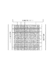
図3はTFTを用いたアクティブ駆動型有機発光素子の一例を示す断面模式図である。ガラス基板上にポリシリコンp−Si層が設けられ、チャネル、ドレイン、ソース領域にはそれぞれ必要な不純物が選択され、ドープされる。この上にゲート絶縁膜を介してゲート電極が設けられると共に、上記ドレイン領域、ソース領域に接続するドレイン電極、ソース電極が形成されている。この時ドレイン電極と画素電極は、介在する絶縁膜に開けたコンタクトホールにより接続される。 FIG. 3 is a schematic cross-sectional view showing an example of an active drive type organic light emitting device using TFTs. A polysilicon p-Si layer is provided on the glass substrate, and necessary impurities are selected and doped in the channel, drain and source regions, respectively. A gate electrode is provided thereon via a gate insulating film, and a drain electrode and a source electrode connected to the drain region and the source region are formed. At this time, the drain electrode and the pixel electrode are connected by a contact hole opened in the intervening insulating film.
上記画素電極上に有機発光層を形成し、陰極を順次積層し、アクティブ型有機発光表示素子を得ることができる。本実施例では、画素電極をアノードとしてCr、さらに60nmのIZO(酸化亜鉛と酸化インジウムの化合物)からなる透明電極をスパッタにより堆積した。これらのCr層およびIZOをパターニングしアノードとした。Cr/IZOアノードの画素サイズは60μm×90μm、画素間部は40μmで100×100ドットの表示装置とした。 An active organic light emitting display element can be obtained by forming an organic light emitting layer on the pixel electrode and sequentially laminating a cathode. In this example, a transparent electrode made of Cr and further 60 nm of IZO (a compound of zinc oxide and indium oxide) was deposited by sputtering using the pixel electrode as an anode. These Cr layers and IZO were patterned to form anodes. A Cr / IZO anode has a pixel size of 60 μm × 90 μm, an inter-pixel portion of 40 μm, and a display device of 100 × 100 dots.
<実施例1>
上記構成のアノードを備えたTFT基板を用意し、アノード上に、正孔輸送材料として下記構造式で示される化合物1を用いて真空蒸着法にて成膜を行った。蒸着時の真空度は5.0×10⁻⁵Pa、成膜速度は0.1〜0.2nm/secの条件で成膜した。形成されたホール輸送層の厚みは20nmであった。
<Example 1>
A TFT substrate provided with the anode having the above structure was prepared, and a film was formed on the anode by a vacuum deposition method using Compound 1 represented by the following structural formula as a hole transport material. The degree of vacuum during vapor deposition was 5.0 × 10 −5 Pa, and the film formation rate was 0.1 to 0.2 nm / sec. The thickness of the formed hole transport layer was 20 nm.

(赤発光層の作製)
まず、2次元方向に多数配置された画素のうち、赤色発光部にのみ開口部を有する蒸着マスクを入れた。
(Preparation of red light emitting layer)
First, a vapor deposition mask having an opening only in a red light emitting portion among a plurality of pixels arranged in a two-dimensional direction was put.
下記構造式で示される化合物2をホストとして用いて下記構造式で示される化合物3とを共蒸着(重量比93:7)して、厚み25nmの発光層を設けた。 Using a compound 2 represented by the following structural formula as a host, a compound 3 represented by the following structural formula was co-evaporated (weight ratio 93: 7) to provide a light-emitting layer having a thickness of 25 nm.
(緑発光層の作製)
多数配置された画素のうち緑色発光部にのみ開口部を有する蒸着マスクを入れた。
次に、発光層のホストとして下記に示す化合物4と、下記に示す発光性化合物5を共蒸着(重量比90:10)して25nmの発光層を設けた。
(Production of green light emitting layer)
A vapor deposition mask having an opening only in a green light emitting portion among a large number of arranged pixels was inserted.
Next, a compound 4 shown below as a host of the light emitting layer and a light emitting compound 5 shown below were co-deposited (weight ratio 90:10) to provide a 25 nm light emitting layer.
(青発光層の作製)
多数配置された画素のうち青色発光部にのみ開口部を有する蒸着マスクを入れた。
次に、発光層のホストとして下記示す化合物6と、下記に示す発光性化合物7を共蒸着(重量比90:10)して25nmの発光層3を設けた。
(Preparation of blue light-emitting layer)
A vapor deposition mask having an opening only in a blue light emitting portion among a large number of arranged pixels was inserted.
Next, the compound 6 shown below as a host of the light emitting layer and the light emitting compound 7 shown below were co-evaporated (weight ratio 90:10) to provide the light emitting layer 3 of 25 nm.
(電子輸送層・電子注入層の作製)
まず、蒸着マスクを取り外して、画素部全面に蒸着できるようにした。
電子輸送層として下記に示す化合物8を蒸着して10nmの電子輸送層を設けた。
(Preparation of electron transport layer and electron injection layer)
First, the deposition mask was removed so that the entire surface of the pixel portion could be deposited.
The following compound 8 was deposited as an electron transport layer to provide a 10 nm electron transport layer.
次に、アルカリディスペンサに封入された金属セシウムと上記化合物8を共蒸着(重量比90:10)して40nmの電子注入層を設けた。 Next, metal cesium sealed in an alkali dispenser and the compound 8 were co-evaporated (weight ratio 90:10) to provide a 40 nm electron injection layer.
(陰極の作製)
有機化合物層まで成膜した基板を、DCスパッタ装置(大阪真空製)へ移動させ、前記有機化合物層上にインジウム錫酸化物(ITO)をスパッタ法にて2000Å成膜し、透明な発光取り出し陰極電極を得た。スパッタガスとしてアルゴンと酸素の混合ガス(体積比でアルゴン:酸素=200:1)を用い、圧力を0.3Pa、DC出力を40Wとした。以上のようにして、TFTを有するRGBの有機EL素子を得た。
(Preparation of cathode)
The substrate on which the organic compound layer was formed was moved to a DC sputtering apparatus (manufactured by Osaka Vacuum Co., Ltd.), and 2000 mm of indium tin oxide (ITO) was formed on the organic compound layer by sputtering, and a transparent light emitting cathode was obtained. An electrode was obtained. A mixed gas of argon and oxygen (volume ratio: argon: oxygen = 200: 1) was used as the sputtering gas, the pressure was 0.3 Pa, and the DC output was 40 W. As described above, an RGB organic EL element having TFTs was obtained.
素子作製後、露点−90℃以下のグローブボックス内において、UV硬化樹脂で本素子とガラス基板を貼り合わせて封止した。 After the device was fabricated, the device and the glass substrate were bonded and sealed with a UV curable resin in a glove box having a dew point of −90 ° C. or less.
このようにして、TFT基板上に、ホール注入層、ホール輸送層、発光層、電子輸送層、有機化合物層および透明陰極電極を設けたトップエミッション型RGBフルカラー有機ELパネルを得た。 Thus, a top emission type RGB full color organic EL panel in which a hole injection layer, a hole transport layer, a light emitting layer, an electron transport layer, an organic compound layer and a transparent cathode electrode were provided on the TFT substrate was obtained.
このフルカラーディスプレイのRGBを点灯させて白色光を点灯させた。
白色は、R:G:B=3:6:1の輝度の時に得られ、CIE色度座標の値は、x=0.30,y=0.32であった。
赤色発光は、発光輝度300cd/m2の時、620nmに発光最大波長をもつ発光が観測され、このときの素子への印加電圧は3.6Vであった。
緑色発光は、発光輝度600cd/m2の時、520nmに発光最大波長をもつ発光が観測され、このときの素子への印加電圧は3.4Vであった。
青色発光は、発光輝度100cd/m2の時、460nmに発光最大波長をもつ発光が観測され、このときの素子への印加電圧は3.2Vであった。
RGB of this full-color display was turned on, and white light was turned on.
White color was obtained when the luminance was R: G: B = 3: 6: 1, and the CIE chromaticity coordinate values were x = 0.30 and y = 0.32.
As for red light emission, light emission having a maximum light emission wavelength of 620 nm was observed at an emission luminance of 300 cd / m 2 , and the voltage applied to the device at this time was 3.6V.
In the case of green light emission, light emission having a maximum light emission wavelength of 520 nm was observed at an emission luminance of 600 cd / m 2 , and the voltage applied to the device at this time was 3.4V.
As for blue light emission, light emission having a maximum light emission wavelength of 460 nm was observed at an emission luminance of 100 cd / m 2 , and the voltage applied to the device at this time was 3.2V.
このときのRGB各素子の特性と、発光層/ホール輸送層および発光層/電子輸送層のイオン化ポテンシャルおよび電子親和力のエネルギーのギャップ値を表1に示した。 Table 1 shows the characteristics of each RGB element and the gap values of the ionization potential and electron affinity energy of the light emitting layer / hole transport layer and the light emitting layer / electron transport layer.
以上のように本実施例の素子はRGBともに4V以下の低電圧で駆動することができた。また、白色を発光させた時のRGB各素子の駆動電圧のばらつきも0.4Vと1V以内に収まっていた。 As described above, the element of this example could be driven at a low voltage of 4 V or less for both RGB. In addition, variation in driving voltage of each element of RGB when white light was emitted was within 0.4V and 1V.
これらのRGBの画素を上記の初期輝度で定電流駆動して輝度半減時間を測定したところ、全ての色で10000時間以上であった。本実施例で用いた材料は全て130℃以上のガラス転移温度を有しているため、耐熱性が高く、車内での長期使用にも耐え得るものであった。 When these RGB pixels were driven at a constant current at the above initial luminance and the luminance half time was measured, it was 10000 hours or more for all colors. Since all the materials used in this example had a glass transition temperature of 130 ° C. or higher, they had high heat resistance and could withstand long-term use in the vehicle.
<実施例2>
実施例1で用いたTFT基板の上に、下記構造式で示される化合物9を用い実施例1と同様にしてホール輸送層を成膜した。形成されたホール輸送層の厚みは20nmであった。
<Example 2>
A hole transport layer was formed on the TFT substrate used in Example 1 in the same manner as in Example 1 using Compound 9 represented by the following structural formula. The thickness of the formed hole transport layer was 20 nm.
(青発光層の作製)
青用のマスクを入れた後、実施例1で使用した化合物2を青のホストとして用いた。実施例1で用いた発光性化合物7をドーパントとして共蒸着(重量比90:10)して25nmの発光層を設けた。
(Preparation of blue light-emitting layer)
After putting a blue mask, the compound 2 used in Example 1 was used as a blue host. The light emitting compound 7 used in Example 1 was co-evaporated as a dopant (weight ratio 90:10) to provide a 25 nm light emitting layer.
(電子輸送層・電子注入層の作製)
実施例1と同様、蒸着マスクを取り外して、画素部全面に蒸着できるようにしたのち、下記構造式で示される化合物10を蒸着して10nmの電子輸送層を設けた。
(Preparation of electron transport layer and electron injection layer)
In the same manner as in Example 1, the deposition mask was removed so that the entire surface of the pixel portion could be deposited, and then a compound 10 represented by the following structural formula was deposited to provide a 10 nm electron transport layer.
更に、電子注入層としてアルカリディスペンサに封入された金属セシウムと上記化合物11を共蒸着(重量比90:10)して40nmの電子注入層を設けた。 Further, metal cesium sealed in an alkali dispenser and the compound 11 were co-deposited (weight ratio 90:10) as an electron injection layer to provide a 40 nm electron injection layer.
以下、実施例1と同様に陰極を設け、封止を行い、電子輸送層がRGBで共通の有機ELディスプレイを得た。得られた素子の特性と各バンドギャップの値を表2に示す
発光層/ホール輸送層のイオン化ポテンシャルの差、および、発光層/電子輸送層の電子親和力の差が共に0.1eV以内に収まっており、発光層へのキャリア注入が非常にスムーズであった。
Thereafter, a cathode was provided and sealed in the same manner as in Example 1 to obtain an organic EL display having an electron transport layer common to RGB. The characteristics of the obtained device and the values of each band gap are shown in Table 2. Both the difference in ionization potential between the light emitting layer / hole transport layer and the difference in electron affinity between the light emitting layer / electron transport layer are within 0.1 eV. The carrier injection into the light emitting layer was very smooth.
また、ホール輸送層の電子親和力が発光層の電子親和力よりも0.2eV以上浅いため発光層に注入された電子がホール輸送層まで漏れることなく発光層内で効率よく再結合し、高い発光効率を示していた。 In addition, since the electron affinity of the hole transport layer is shallower by 0.2 eV or more than the electron affinity of the light emitting layer, electrons injected into the light emitting layer are efficiently recombined in the light emitting layer without leaking to the hole transporting layer, and high light emitting efficiency. Was showing.
一方、発光層のイオン化ポテンシャルが電子輸送層のイオン化ポテンシャルよりも0.2eV以上深いため、発光層に注入されたホールが電子輸送層に漏れることなく発光層内で効率よく再結合し、高い発光効率を示していた。 On the other hand, since the ionization potential of the light-emitting layer is 0.2 eV or more deeper than the ionization potential of the electron transport layer, holes injected into the light-emitting layer recombine efficiently in the light-emitting layer without leaking into the electron transport layer, resulting in high light emission. Showed efficiency.
以上の結果から、同じ輝度で発光させたときの素子に掛かる駆動電圧も実施例1と比較して更に低下しており、TFTの電源のパワーを抑えることができた。RGB間の電圧差も0.1Vに減少したため、TFT駆動時の輝度ばらつきも極めて少なくなった。なお、RGBを表2の輝度で発光させた時のCIE色度座標の値は、x=0.31、y=0.34の良好な白色であった。 From the above results, the driving voltage applied to the element when emitting light with the same luminance was further reduced as compared with Example 1, and the power of the TFT power supply could be suppressed. Since the voltage difference between RGB is also reduced to 0.1 V, the luminance variation when driving the TFT is extremely reduced. Note that the CIE chromaticity coordinate values when RGB was emitted with the luminance shown in Table 2 were good white with x = 0.31 and y = 0.34.
<比較例1>
実施例1で用いたホール輸送材の代わりに下記構造式で示される化合物11を用いた以外は実施例1と同様の有機ELパネルを作成した。
<Comparative Example 1>
An organic EL panel similar to that in Example 1 was prepared except that the compound 11 represented by the following structural formula was used instead of the hole transport material used in Example 1.
得られた素子の特性と各バンドギャップの値を表3に示す。ホール輸送層と発光層のイオン化ポテンシャルのギャップが大きくなった結果、ホールの注入性が低下して高電圧化し、RGBの電圧ばらつきが大きくなってしまった(最大1.1V)。 Table 3 shows characteristics of the obtained element and values of each band gap. As a result of the increase in the gap between the ionization potentials of the hole transport layer and the light emitting layer, the hole injectability is lowered and the voltage is increased, and the voltage variation of RGB is increased (maximum 1.1 V).
<比較例2>
実施例1で用いた電子輸送材の代わりに下記構造式で示される化合物12を用いた以外は実施例1と同様の有機ELパネルを作成した。
<Comparative example 2>
An organic EL panel similar to that in Example 1 was prepared except that the compound 12 represented by the following structural formula was used instead of the electron transport material used in Example 1.
得られた素子の特性とバンドギャップを表4に示す。電子輸送層と発光層の電子親和力のギャップが大きくなった結果、発光層への電子注入性が低下して著しく高電圧化していた。また、発光層と電子輸送層のイオン化ポテンシャルのギャップが小さいため電子輸送層にホールが漏れ、発光効率が低下していた。その結果、白色発光させた時のRGBの電圧ばらつきが1Vを超えてしまった(最大1.3V)。 Table 4 shows the characteristics and band gap of the obtained device. As a result of an increase in the electron affinity gap between the electron transport layer and the light-emitting layer, the electron injection property into the light-emitting layer was lowered and the voltage was significantly increased. Further, since the gap between the ionization potentials of the light emitting layer and the electron transport layer is small, holes leak into the electron transport layer, and the light emission efficiency is lowered. As a result, the RGB voltage variation when white light was emitted exceeded 1 V (maximum 1.3 V).
Claims (3)
前記有機発光素子と前記トランジスタを赤及び緑及び青を発光するために各色毎に有する有機発光素子アレイにおいて、
前記有機発光層に接する正孔輸送層と、
前記有機発光層に接する電子輸送層と、を有し、
前記有機発光層はホスト材料とゲスト材料を有し、
前記正孔輸送層のイオン化ポテンシャルと全ての有機発光素子の前記有機発光層のホスト材料のイオン化ポテンシャルの差が0.2eV以下であり、
前記電子輸送層の電子親和力と全ての有機発光素子の前記有機発光層のホスト材料の電子親和力の差が0.2eV以下であることを特徴とする有機発光素子アレイ。 An organic light emitting device having an organic light emitting layer and a pair of electrodes disposed between the organic light emitting layers, and a transistor for controlling light emission non-emission of the organic light emitting device,
In the organic light emitting element array having the organic light emitting element and the transistor for each color in order to emit red, green and blue,
A hole transport layer in contact with the organic light emitting layer;
An electron transport layer in contact with the organic light emitting layer,
The organic light emitting layer has a host material and a guest material,
The difference between the ionization potential of the hole transport layer and the ionization potential of the host material of the organic light emitting layer of all organic light emitting devices is 0.2 eV or less,
An organic light emitting device array, wherein a difference between an electron affinity of the electron transport layer and an electron affinity of a host material of the organic light emitting layer of all organic light emitting devices is 0.2 eV or less.
(全ての有機発光素子の前記有機発光層のホスト材料の電子親和力の絶対値)−(前記正孔輸送層の電子親和力の絶対値)≧0.2eV
であることを特徴とする請求項1に記載の有機発光素子アレイ。 The absolute value of the electron affinity of the hole transport layer and the absolute value of the electron affinity of the host material of the organic light emitting layer of all organic light emitting elements are:
(Absolute value of electron affinity of host material of organic light emitting layer of all organic light emitting elements) − (Absolute value of electron affinity of hole transport layer) ≧ 0.2 eV
The organic light-emitting element array according to claim 1, wherein
(前記電子輸送層のイオン化ポテンシャルの絶対値)−(全ての有機発光素子の前記有機発光層のホスト材料のイオン化ポテンシャルの絶対値)≧0.2eV
であることを特徴とする請求項1に記載の有機発光素子アレイ。
The absolute value of the ionization potential of the electron transport layer and the absolute value of the ionization potential of the host material of the organic light emitting layer of all organic light emitting devices are:
(Absolute value of ionization potential of the electron transport layer) − (Absolute value of ionization potential of the host material of the organic light emitting layer of all organic light emitting devices) ≧ 0.2 eV
The organic light-emitting element array according to claim 1, wherein
Priority Applications (3)
| Application Number | Priority Date | Filing Date | Title |
|---|---|---|---|
| JP2006087015A JP2007266160A (en) | 2006-03-28 | 2006-03-28 | Organic light emitting element array |
| PCT/JP2007/055308 WO2007111153A1 (en) | 2006-03-28 | 2007-03-09 | Organic light emitting device array |
| US11/917,119 US7794857B2 (en) | 2006-03-28 | 2007-03-09 | Organic light emitting device array |
Applications Claiming Priority (1)
| Application Number | Priority Date | Filing Date | Title |
|---|---|---|---|
| JP2006087015A JP2007266160A (en) | 2006-03-28 | 2006-03-28 | Organic light emitting element array |
Publications (2)
| Publication Number | Publication Date |
|---|---|
| JP2007266160A true JP2007266160A (en) | 2007-10-11 |
| JP2007266160A5 JP2007266160A5 (en) | 2009-06-18 |
Family
ID=38541074
Family Applications (1)
| Application Number | Title | Priority Date | Filing Date |
|---|---|---|---|
| JP2006087015A Pending JP2007266160A (en) | 2006-03-28 | 2006-03-28 | Organic light emitting element array |
Country Status (3)
| Country | Link |
|---|---|
| US (1) | US7794857B2 (en) |
| JP (1) | JP2007266160A (en) |
| WO (1) | WO2007111153A1 (en) |
Cited By (5)
| Publication number | Priority date | Publication date | Assignee | Title |
|---|---|---|---|---|
| WO2009119884A1 (en) * | 2008-03-26 | 2009-10-01 | Canon Kabushiki Kaisha | Organic light emitting device |
| JP2012207304A (en) * | 2011-03-14 | 2012-10-25 | Semiconductor Energy Lab Co Ltd | Successive deposition apparatus and successive deposition method |
| US8754399B2 (en) | 2010-07-08 | 2014-06-17 | Mitsubishi Chemical Corporation | Organic electroluminescence element, organic electroluminescence device, organic el display device, and organic el lighting |
| WO2021192159A1 (en) * | 2020-03-26 | 2021-09-30 | シャープ株式会社 | Light-emitting element and display device |
| WO2021192158A1 (en) * | 2020-03-26 | 2021-09-30 | シャープ株式会社 | Light emitting element and display device |
Families Citing this family (4)
| Publication number | Priority date | Publication date | Assignee | Title |
|---|---|---|---|---|
| JP5511157B2 (en) * | 2008-07-03 | 2014-06-04 | キヤノン株式会社 | Luminescent display device |
| KR100994118B1 (en) | 2009-01-13 | 2010-11-15 | 삼성모바일디스플레이주식회사 | Organic light emitting diode and manufacturing method thereof |
| KR20100095666A (en) * | 2009-02-12 | 2010-09-01 | 서울반도체 주식회사 | Light emitting diode chip for high voltage operation and light emitting diode package having the same |
| KR102115477B1 (en) * | 2013-08-14 | 2020-05-27 | 삼성디스플레이 주식회사 | Organic compound and organic light emitting diode device including the same |
Citations (5)
| Publication number | Priority date | Publication date | Assignee | Title |
|---|---|---|---|---|
| JP2000150152A (en) * | 1998-11-16 | 2000-05-30 | Toyo Ink Mfg Co Ltd | Organic electroluminescence display device |
| JP2003151769A (en) * | 2001-08-28 | 2003-05-23 | Konica Corp | Multicolor light emission device and its manufacturing method |
| JP2003257677A (en) * | 2002-03-04 | 2003-09-12 | Honda Motor Co Ltd | Organic electroluminescence element and its manufacturing method |
| JP2005026210A (en) * | 2003-06-10 | 2005-01-27 | Fujitsu Ltd | Organic el element |
| JP2005310742A (en) * | 2004-03-25 | 2005-11-04 | Sanyo Electric Co Ltd | Organic electroluminescent element |
Family Cites Families (10)
| Publication number | Priority date | Publication date | Assignee | Title |
|---|---|---|---|---|
| JPH04297076A (en) | 1991-01-31 | 1992-10-21 | Toshiba Corp | Organic el element |
| JP3249297B2 (en) * | 1994-07-14 | 2002-01-21 | 三洋電機株式会社 | Organic electroluminescent device |
| JP2689917B2 (en) | 1994-08-10 | 1997-12-10 | 日本電気株式会社 | Active matrix type current control type light emitting element drive circuit |
| JPH1039791A (en) | 1996-07-22 | 1998-02-13 | Mitsubishi Electric Corp | Organic electroluminescence display device |
| US6791258B2 (en) * | 2001-06-21 | 2004-09-14 | 3M Innovative Properties Company | Organic light emitting full color display panel |
| EP2555274B1 (en) | 2001-08-29 | 2020-06-24 | The Trustees of Princeton University | Organic light emitting devices having carrier blocking layers comprising metal complexes |
| JP3902993B2 (en) * | 2002-08-27 | 2007-04-11 | キヤノン株式会社 | Fluorene compound and organic light emitting device using the same |
| JP4125076B2 (en) * | 2002-08-30 | 2008-07-23 | キヤノン株式会社 | Monoaminofluorene compound and organic light-emitting device using the same |
| JP2004214180A (en) | 2002-12-16 | 2004-07-29 | Canon Inc | Organic light-emitting element |
| JP4086817B2 (en) | 2004-07-20 | 2008-05-14 | キヤノン株式会社 | Organic EL device |
-
2006
- 2006-03-28 JP JP2006087015A patent/JP2007266160A/en active Pending
-
2007
- 2007-03-09 US US11/917,119 patent/US7794857B2/en not_active Expired - Fee Related
- 2007-03-09 WO PCT/JP2007/055308 patent/WO2007111153A1/en active Application Filing
Patent Citations (5)
| Publication number | Priority date | Publication date | Assignee | Title |
|---|---|---|---|---|
| JP2000150152A (en) * | 1998-11-16 | 2000-05-30 | Toyo Ink Mfg Co Ltd | Organic electroluminescence display device |
| JP2003151769A (en) * | 2001-08-28 | 2003-05-23 | Konica Corp | Multicolor light emission device and its manufacturing method |
| JP2003257677A (en) * | 2002-03-04 | 2003-09-12 | Honda Motor Co Ltd | Organic electroluminescence element and its manufacturing method |
| JP2005026210A (en) * | 2003-06-10 | 2005-01-27 | Fujitsu Ltd | Organic el element |
| JP2005310742A (en) * | 2004-03-25 | 2005-11-04 | Sanyo Electric Co Ltd | Organic electroluminescent element |
Cited By (7)
| Publication number | Priority date | Publication date | Assignee | Title |
|---|---|---|---|---|
| WO2009119884A1 (en) * | 2008-03-26 | 2009-10-01 | Canon Kabushiki Kaisha | Organic light emitting device |
| US8754399B2 (en) | 2010-07-08 | 2014-06-17 | Mitsubishi Chemical Corporation | Organic electroluminescence element, organic electroluminescence device, organic el display device, and organic el lighting |
| JP2012207304A (en) * | 2011-03-14 | 2012-10-25 | Semiconductor Energy Lab Co Ltd | Successive deposition apparatus and successive deposition method |
| US9263705B2 (en) | 2011-03-14 | 2016-02-16 | Semiconductor Energy Laboratory Co., Ltd. | Successive deposition apparatus and successive deposition method |
| WO2021192159A1 (en) * | 2020-03-26 | 2021-09-30 | シャープ株式会社 | Light-emitting element and display device |
| WO2021192158A1 (en) * | 2020-03-26 | 2021-09-30 | シャープ株式会社 | Light emitting element and display device |
| CN115298723A (en) * | 2020-03-26 | 2022-11-04 | 夏普株式会社 | Light-emitting element and display device |
Also Published As
| Publication number | Publication date |
|---|---|
| US7794857B2 (en) | 2010-09-14 |
| WO2007111153A1 (en) | 2007-10-04 |
| US20090033211A1 (en) | 2009-02-05 |
Similar Documents
| Publication | Publication Date | Title |
|---|---|---|
| JP2020123592A (en) | Rgbw oled display for extended lifetime and reduced power consumption | |
| CN100440528C (en) | Circuit arrangement for AC driving of organic diodes | |
| US7760165B2 (en) | Control circuit for stacked OLED device | |
| US7935963B2 (en) | Hybrid organic light emitting diode | |
| JP4181795B2 (en) | Electroluminescence element | |
| JP2007266160A (en) | Organic light emitting element array | |
| JP5094477B2 (en) | Organic light-emitting display device and method for manufacturing the same | |
| TWI536360B (en) | Method for driving quad-subpixel display | |
| JP5194699B2 (en) | Organic electroluminescence device and electronic device | |
| JP2005317506A (en) | Organic electroluminescent display | |
| JP4411288B2 (en) | Display device | |
| JP2007011063A (en) | Organic electroluminescence display device | |
| JP2009093982A (en) | Organic electroluminescent device, and electronic equipment | |
| KR102000292B1 (en) | Organic light emitting display device and method for manufacturing thereof | |
| JP2003323155A (en) | Driving method of electroluminescent element | |
| KR20040034417A (en) | Organic electroluminescent device, method for manufacturing the organic electroluminescent device, and organic electroluminescent display apparatus | |
| US20120025732A1 (en) | Light emitting device and method for driving the same | |
| JP3669333B2 (en) | Organic electroluminescent device and display device | |
| JP2004281087A (en) | Organic el device and organic el display | |
| KR100547055B1 (en) | Organic Electroluminescent Device | |
| KR100864758B1 (en) | Full color organic electroluminescence device | |
| JP2010277949A (en) | Organic el display device and method of manufacturing the same | |
| JP2018120726A (en) | Organic EL display | |
| JP2008205174A (en) | Organic el element array | |
| US20040155579A1 (en) | Organic electro-luminescent display device and fabrication method thereof |
Legal Events
| Date | Code | Title | Description |
|---|---|---|---|
| A621 | Written request for application examination |
Free format text: JAPANESE INTERMEDIATE CODE: A621 Effective date: 20090330 |
|
| A521 | Request for written amendment filed |
Free format text: JAPANESE INTERMEDIATE CODE: A523 Effective date: 20090422 |
|
| RD04 | Notification of resignation of power of attorney |
Free format text: JAPANESE INTERMEDIATE CODE: A7424 Effective date: 20100201 |
|
| RD01 | Notification of change of attorney |
Free format text: JAPANESE INTERMEDIATE CODE: A7421 Effective date: 20100630 |
|
| A131 | Notification of reasons for refusal |
Free format text: JAPANESE INTERMEDIATE CODE: A131 Effective date: 20120403 |
|
| A02 | Decision of refusal |
Free format text: JAPANESE INTERMEDIATE CODE: A02 Effective date: 20120731 |