JP2007166320A - Solid-state imaging device and driving method thereof - Google Patents
Solid-state imaging device and driving method thereof Download PDFInfo
- Publication number
- JP2007166320A JP2007166320A JP2005360898A JP2005360898A JP2007166320A JP 2007166320 A JP2007166320 A JP 2007166320A JP 2005360898 A JP2005360898 A JP 2005360898A JP 2005360898 A JP2005360898 A JP 2005360898A JP 2007166320 A JP2007166320 A JP 2007166320A
- Authority
- JP
- Japan
- Prior art keywords
- transistor
- signal
- imaging device
- signal line
- state imaging
- Prior art date
- Legal status (The legal status is an assumption and is not a legal conclusion. Google has not performed a legal analysis and makes no representation as to the accuracy of the status listed.)
- Granted
Links
Images

Classifications
-
- H—ELECTRICITY
- H04—ELECTRIC COMMUNICATION TECHNIQUE
- H04N—PICTORIAL COMMUNICATION, e.g. TELEVISION
- H04N25/00—Circuitry of solid-state image sensors [SSIS]; Control thereof
- H04N25/70—SSIS architectures; Circuits associated therewith
- H04N25/76—Addressed sensors, e.g. MOS or CMOS sensors
- H04N25/767—Horizontal readout lines, multiplexers or registers
-
- H—ELECTRICITY
- H04—ELECTRIC COMMUNICATION TECHNIQUE
- H04N—PICTORIAL COMMUNICATION, e.g. TELEVISION
- H04N25/00—Circuitry of solid-state image sensors [SSIS]; Control thereof
- H04N25/70—SSIS architectures; Circuits associated therewith
- H04N25/76—Addressed sensors, e.g. MOS or CMOS sensors
-
- H—ELECTRICITY
- H04—ELECTRIC COMMUNICATION TECHNIQUE
- H04N—PICTORIAL COMMUNICATION, e.g. TELEVISION
- H04N25/00—Circuitry of solid-state image sensors [SSIS]; Control thereof
- H04N25/70—SSIS architectures; Circuits associated therewith
- H04N25/76—Addressed sensors, e.g. MOS or CMOS sensors
- H04N25/78—Readout circuits for addressed sensors, e.g. output amplifiers or A/D converters
-
- H—ELECTRICITY
- H04—ELECTRIC COMMUNICATION TECHNIQUE
- H04N—PICTORIAL COMMUNICATION, e.g. TELEVISION
- H04N25/00—Circuitry of solid-state image sensors [SSIS]; Control thereof
- H04N25/60—Noise processing, e.g. detecting, correcting, reducing or removing noise
- H04N25/67—Noise processing, e.g. detecting, correcting, reducing or removing noise applied to fixed-pattern noise, e.g. non-uniformity of response
-
- H—ELECTRICITY
- H04—ELECTRIC COMMUNICATION TECHNIQUE
- H04N—PICTORIAL COMMUNICATION, e.g. TELEVISION
- H04N25/00—Circuitry of solid-state image sensors [SSIS]; Control thereof
- H04N25/70—SSIS architectures; Circuits associated therewith
- H04N25/76—Addressed sensors, e.g. MOS or CMOS sensors
- H04N25/77—Pixel circuitry, e.g. memories, A/D converters, pixel amplifiers, shared circuits or shared components
Landscapes
- Engineering & Computer Science (AREA)
- Multimedia (AREA)
- Signal Processing (AREA)
- Transforming Light Signals Into Electric Signals (AREA)
- Solid State Image Pick-Up Elements (AREA)
Abstract
【課題】フォトダイオードからの信号電荷の読み出しを制御する読み出しトランジスタの動作時に起こるカップリングに起因する画像不良を抑制することが可能な固体撮像装置及びその駆動方法を提供する。
【解決手段】増幅型固体撮像装置であって、フォトダイオード11の信号電荷を読み出す読み出しトランジスタ12を有し、信号電荷に対応する増幅信号を出力する単位セル10と、単位セル10と接続された第1の垂直信号線109及び第2の垂直信号線203と、第1の垂直信号線109及び第2の垂直信号線203を介して伝達される増幅信号を蓄積するサンプリング容量205と、読み出しトランジスタ12による信号電荷の読み出しの開始及び終了のいずれかにおいて、単位セル10の増幅信号のサンプリング容量205への伝達を防止するバイアス電流源116、カップリング制御用トランジスタ115及びカップリング制御回路117とを備える。
【選択図】図1A solid-state imaging device capable of suppressing image defects caused by coupling that occurs during operation of a readout transistor that controls readout of signal charges from a photodiode, and a driving method thereof.
An amplification type solid-state imaging device having a readout transistor for reading out signal charges of a photodiode, a unit cell for outputting an amplified signal corresponding to the signal charge, and a unit cell connected to the unit cell. A first vertical signal line 109 and a second vertical signal line 203; a sampling capacitor 205 for storing an amplified signal transmitted via the first vertical signal line 109 and the second vertical signal line 203; and a read transistor 12, a bias current source 116, a coupling control transistor 115, and a coupling control circuit 117 that prevent transmission of the amplified signal of the unit cell 10 to the sampling capacitor 205 at any of the start and end of reading of the signal charge by 12. Prepare.
[Selection] Figure 1
Description
本発明は、固体撮像装置及びその駆動方法に関し、特に増幅型固体撮像装置及びその駆動方法に関する。 The present invention relates to a solid-state imaging device and a driving method thereof, and more particularly to an amplification type solid-state imaging device and a driving method thereof.
近年、固体撮像装置の一つとして、MOS型の撮像素子を用いた増幅型固体撮像装置が注目されている。この固体撮像装置は、画素を表すセル毎に設けられ、フォトダイオードで検出した信号を増幅する増幅トランジスタを備え、高感度という特徴を持つ。この固体撮像装置においては、高画素化(メガピクセル化)による画像の高画質化が要求されている。 In recent years, an amplification-type solid-state imaging device using a MOS-type imaging device has attracted attention as one of solid-state imaging devices. This solid-state imaging device includes an amplification transistor that is provided for each cell representing a pixel and amplifies a signal detected by a photodiode, and has a feature of high sensitivity. In this solid-state imaging device, it is required to improve the image quality by increasing the number of pixels (increasing megapixels).
このような固体撮像装置に関し、二次元に配列された画素を有する固体撮像装置において、転送選択スイッチを設けなくても画素の選択/非選択を行うことが可能な固体撮像装置が、例えば、特許文献1で提案されている。
With regard to such a solid-state imaging device, a solid-state imaging device having pixels arranged in two dimensions and capable of selecting / deselecting a pixel without providing a transfer selection switch is disclosed in, for example, a patent. It is proposed in
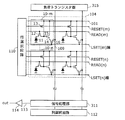
以下に、特許文献1に記載の固体撮像装置について説明する。図12は、特許文献1に記載の固体撮像装置の回路構成を示す図である。
The solid-state imaging device described in
この固体撮像装置は、フォトダイオード21、読み出しトランジスタ22、リセットトランジスタ23、増幅トランジスタ24、垂直選択トランジスタ26、及び増幅トランジスタ24のゲートに直結するフローティングディフュージョン部(以下FD部という)25からなる複数の単位セル20を行列状に配置してなるイメージエリア504と、単位セル20を行単位で選択する行選択回路510と、信号処理部511に単位セル20の信号電圧を列単位で伝達する第1の垂直信号線509と、第1の垂直信号線509を介して伝達された信号電圧を保持し、ノイズをカットする信号処理部511と、単位セル20を列単位で選択する列選択回路512と、信号処理部511から出力された信号電圧を出力アンプ514に伝達する水平信号線513と、出力アンプ514と、負荷トランジスタ群515とから構成される。
This solid-state imaging device includes a plurality of
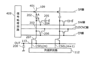
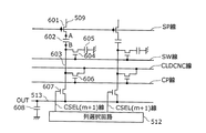
図13は、信号処理部511の回路構成を示す図である。図13では、図12に示した固体撮像装置のイメージエリア504に対応して、2列分の画素と接続された垂直信号線が示されている。
FIG. 13 is a diagram illustrating a circuit configuration of the
信号処理部511は、第1の垂直信号線509と接続されたサンプルホールドトランジスタ601と、サンプルホールドトランジスタ601を介して第1の垂直信号線509に接続されたクランプ容量602と、クランプ容量602を介して第1の垂直信号線509に接続された第2の垂直信号線603と、第2の垂直信号線603と接続されたサンプリングトランジスタ604と、サンプリングトランジスタ604を介して第2の垂直信号線603と接続されたサンプリング容量605と、クランプ容量602及びサンプリングトランジスタ604に接続されたクランプトランジスタ606と、第2の垂直信号線603に接続された列選択トランジスタ607と、水平信号線513と接続された水平信号線容量608とから構成される。
The
サンプルホールドトランジスタ601は、SP線をハイレベルにするサンプリングパルスの印加に対応して、ON状態となり、第1の垂直信号線509により伝達された信号電圧をクランプ容量602に伝達する。
The
第2の垂直信号線603は、第1の垂直信号線509からクランプ容量602を介して伝達された信号電圧を伝達する。
The second
サンプリングトランジスタ604は、SW線をハイレベルにする容量選択パルスの印加に対応して、ON状態となり、第2の垂直信号線603により伝達された信号電圧をサンプリング容量605に転送する。
The sampling transistor 604 is turned on in response to the application of the capacitance selection pulse for setting the SW line to the high level, and transfers the signal voltage transmitted through the second
クランプトランジスタ606は、CP線をハイレベルにするクランプパルスの印加に対応して、ON状態となり、第2の垂直信号線603と、クランプ容量602と、サンプリング容量605とをCLDCNC線の電位にリセットする。クランプ容量602はリセット時の端子A―B間の電圧を保持することで、単位セル20毎で異なる固定パターンノイズを除去する。
The
列選択トランジスタ607は、CSEL線をハイレベルにする列選択パルスの印加に対応して、順次ON状態となり、サンプリング容量605に蓄積された信号電圧を水平信号線513に転送する。
The
サンプリング容量605は、各行毎に読み出された信号電圧を保持する。
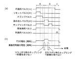
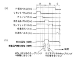
以上のような従来の固体撮像装置の動作について、図14(a)に示す駆動タイミングチャートに沿って説明する。
The
The operation of the conventional solid-state imaging device as described above will be described along the drive timing chart shown in FIG.
m行目の単位セル20が選択されると、LSET(m)線をハイレベルにする行選択パルス(m)がm行目の単位セル20の垂直選択トランジスタ26に印加される。垂直選択トランジスタ26はON状態となり、増幅トランジスタ24と負荷トランジスタ群515とでソースフォロア回路が形成され、単位セル20の画素電源に追従した電圧がソースフォロア回路から第1の垂直信号線509に出力される。
When the
次に、SP線をハイレベルにするサンプリングパルスがサンプルホールドトランジスタ601に印加される。サンプルホールドトランジスタ601は、ON状態となり、ソースフォロア回路から第1の垂直信号線509に出力された電圧がクランプ容量602に保持される。このとき、CP線をハイレベルにするクランプパルスがクランプトランジスタ606に印加される。クランプトランジスタ606はON状態となり、クランプ容量602の第2の垂直信号線603側がCLDCNC線の電位にリセットされる。また、同時にSW線をハイレベルにする容量選択パルスが印加されているので、サンプリングトランジスタ604はON状態となり、サンプリング容量605がCLDCNC線の電位にリセットされる。
Next, a sampling pulse for setting the SP line to a high level is applied to the
次に、RESET(m)線をハイレベルにするリセットパルス(m)がリセットトランジスタ23に印加される。リセットトランジスタ23はON状態となり、FD部25の電位がリセットされる。FD部25に接続している増幅トランジスタ24のゲート電圧はFD部25の電位となり、この電圧に応じた電圧、具体的には(FD部の電位−Vt)×αで与えられる電圧が第1の垂直信号線509に出力される。ここで、Vtは増幅トランジスタ24の閾値電圧であり、αは電圧増幅率である。
Next, a reset pulse (m) that sets the RESET (m) line to a high level is applied to the
次に、CP線をローレベルにするクランプパルスがクランプトランジスタ606に印加され、クランプトランジスタ606がOFF状態となり、第2の垂直信号線603の電位はフローティング状態となる。
Next, a clamp pulse for lowering the CP line is applied to the
次に、READ(m)線をハイレベルにする読み出しパルス(m)が読み出しトランジスタ22に印加される。読み出しトランジスタ22はON状態となり、フォトダイオード21に蓄積した信号電荷がFD部25に転送される。FD部25に接続している増幅トランジスタ24のゲート電圧はFD部25の電位となり、この電圧に応じた電圧、具体的には(FD部の電位−Vt)×αで与えられる電圧が第1の垂直信号線509に出力される。このとき、CP線をローレベルにするクランプパルスがクランプトランジスタ606に印加されているので、クランプトランジスタ606はOFF状態となり、サンプリング容量605には、FD部25の電位がリセットされたときに第1の垂直信号線509に出力された電圧と、フォトダイオード21に蓄積された信号電荷がFD部25に転送されたときに第1の垂直信号線509に出力された電圧との差に応じた電圧変化がm行目の単位セル20の信号電圧として蓄積される。
Next, a read pulse (m) that sets the READ (m) line to a high level is applied to the read transistor 22. The read transistor 22 is turned on, and the signal charge accumulated in the
次に、CSEL(m)線をハイレベルにする列選択パルス(m)、CSEL(m+1)線をハイレベルにする列選択パルス(m+1)、・・・が列選択トランジスタ607に順次印加され、各列選択トランジスタ607は順次ON状態となり、サンプリング容量605に蓄積された信号電圧が水平信号線513に順次出力される。
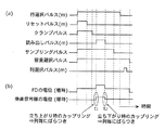
ところで、従来の増幅型固体撮像装置の駆動タイミングでは、読み出しトランジスタのON時およびOFF時の動作においてFD部へのカップリングが発生する。すなわち、垂直信号線における読み出しトランジスタのカップリングの影響により、画質に不具合が発生する。 By the way, at the drive timing of the conventional amplification type solid-state imaging device, coupling to the FD portion occurs in the operation when the readout transistor is ON and OFF. In other words, a problem occurs in image quality due to the coupling of the read transistor in the vertical signal line.
以下に、その画像不具合の詳細について説明する。図14(b)は、フォトダイオード21に信号電荷が蓄積されていない暗時において、図12で示した固体撮像装置の読み出しトランジスタ22に印加される読み出しパルスがローレベルからハイレベル又はハイレベルからローレベルに変化した場合のFD部25の電位変化の状態と第1垂直信号線509の電位変化の状態とを示す図である。
Details of the image defect will be described below. FIG. 14B shows a case where the readout pulse applied to the readout transistor 22 of the solid-state imaging device shown in FIG. 12 from low level to high level or high level in the dark when no signal charge is accumulated in the
図14(b)に示されるように、読み出しパルスがローレベルからハイレベルになり、読み出しトランジスタ22がON状態となる場合(図14におけるt1)、読み出しトランジスタ22のゲートとソース間の容量を介してのFD部25へのカップリングにより、FD部25の電位が上がる。その結果、ソースフォロワを介して第1の垂直信号線509の電位が上昇し、この状態においてサンプリングパルスがハイレベル状態になっているので、第2の垂直信号線603の電位も変化を受ける。
As shown in FIG. 14B, when the read pulse changes from low level to high level and the read transistor 22 is turned on (t 1 in FIG. 14), the capacitance between the gate and source of the read transistor 22 is increased. The potential of the FD
また、図14(b)に示されるように、読み出しパルスがハイレベルからローレベルになり、読み出しトランジスタ22がOFF状態となる場合(図14におけるt2)、読み出しトランジスタ22のゲートとソース間を介してのFD部25へのカップリングにより、FD部25の電位が下がる。その結果、ソースフォロワを介して第1の垂直信号線509の電位が上昇し、この状態においてサンプリングパルスがハイレベル状態になっているので、第2の垂直信号線603の電位も変化を受ける。
Further, as shown in FIG. 14B, when the reading pulse changes from the high level to the low level and the reading transistor 22 is turned off (t 2 in FIG. 14), the gate and the source of the reading transistor 22 are connected. The potential of the
すなわち、従来の増幅型固体撮像装置では、読み出しトランジスタ22を動作させるための電位変化のカップリングにより、第2の垂直信号線603の電位が変化する。読み出しトランジスタ22のカップリング量は各列でばらつくため、各列の第2の垂直信号線603の電位変化にもばらつきが生じる。従って、列選択回路512により各列の信号成分を取り出し出力させると、列毎の出力にばらつきが生じるので、結果として従来の増幅型固体撮像装置は画像不良という課題を有している。
That is, in the conventional amplification type solid-state imaging device, the potential of the second
そこで、本発明は、かかる問題点に鑑み、フォトダイオードからの信号電荷の読み出しを制御する読み出しトランジスタの動作時に起こるカップリングに起因する画像不良を抑制することが可能な固体撮像装置及びその駆動方法を提供することを目的とする。 Therefore, in view of such a problem, the present invention provides a solid-state imaging device capable of suppressing image defects caused by coupling that occurs during operation of a readout transistor that controls readout of signal charges from a photodiode, and a driving method thereof. The purpose is to provide.
上記目的を達成するために、本発明の固体撮像装置は、増幅型固体撮像装置であって、光を信号電荷に変換して蓄積するフォトダイオードと、前記フォトダイオードの信号電荷を読み出す読み出しトランジスタとを有し、信号電荷に対応する増幅信号を出力する単位セルと、前記単位セルと接続された信号線と、前記信号線を介して伝達される前記増幅信号を蓄積する蓄積素子と、前記読み出しトランジスタによる前記信号電荷の読み出しの開始、及び前記読み出しトランジスタによる前記信号電荷の読み出しの終了のいずれかにおいて、前記単位セルの増幅信号の前記蓄積素子への伝達を防止する伝達防止手段とを備えることを特徴とする。ここで、前記伝達防止手段は、前記単位セルと前記蓄積素子との間の信号線に接続された定電圧源と、前記定電圧源と前記信号線との間に挿入された第1伝達防止トランジスタと、前記第1伝達防止トランジスタを制御する第1制御手段であってもよい。 In order to achieve the above object, a solid-state imaging device of the present invention is an amplifying solid-state imaging device, a photodiode for storing light by converting it into a signal charge, a readout transistor for reading out the signal charge of the photodiode, A unit cell that outputs an amplified signal corresponding to a signal charge, a signal line connected to the unit cell, a storage element that stores the amplified signal transmitted through the signal line, and the readout Transmission preventing means for preventing transmission of the amplified signal of the unit cell to the storage element at any one of the start of reading of the signal charge by the transistor and the end of reading of the signal charge by the read transistor; It is characterized by. Here, the transmission preventing means includes a constant voltage source connected to a signal line between the unit cell and the storage element, and a first transmission prevention inserted between the constant voltage source and the signal line. The first control means may control the transistor and the first transmission preventing transistor.
また、本発明は、光を信号電荷に変換して蓄積するフォトダイオードと、前記フォトダイオードの信号電荷を読み出す読み出しトランジスタとを有し、信号電荷に対応する増幅信号を出力する単位セルと、前記単位セルと接続された信号線と、前記信号線を介して伝達される前記増幅信号を蓄積する蓄積素子と、前記単位セルと前記蓄積素子との間の信号線に接続された定電圧源と、前記定電圧源と前記信号線との間に挿入された第1伝達防止トランジスタと、前記第1伝達防止トランジスタを制御する第1制御手段とを備える増幅型固体撮像装置の駆動方法であって、前記第1制御手段は、前記読み出しトランジスタによる前記信号電荷の読み出しの開始、及び前記読み出しトランジスタによる前記信号電荷の読み出しの終了のいずれかにおいて、前記第1伝達防止トランジスタがオフ状態になるように制御することを特徴とする固体撮像装置の駆動方法とすることもできる。 The present invention also includes a photodiode that converts light into signal charges and stores the light, and a readout transistor that reads the signal charges of the photodiode, and outputs a unit cell that outputs an amplified signal corresponding to the signal charges; A signal line connected to the unit cell, a storage element for storing the amplified signal transmitted through the signal line, and a constant voltage source connected to the signal line between the unit cell and the storage element; A method for driving an amplifying solid-state imaging device, comprising: a first transmission preventing transistor inserted between the constant voltage source and the signal line; and first control means for controlling the first transmission preventing transistor. The first control means either starts reading the signal charge by the read transistor or ends reading the signal charge by the read transistor. There are, first transmission prevention transistor may be a method for driving the solid-state imaging device and controls to turn off state.
これによって、読み出しトランジスタのゲートの電圧変化が信号線に伝達することを抑制し、読み出しトランジスタの動作時に起こるカップリングの影響が信号線に伝達するのを抑制できるので、読み出しトランジスタの動作時に起こるカップリングに起因する画像不良を抑制することができる。 As a result, it is possible to suppress the change in the voltage of the gate of the read transistor from being transmitted to the signal line, and to suppress the influence of the coupling that occurs during the operation of the read transistor from being transmitted to the signal line. Image defects caused by the ring can be suppressed.
本発明によれば、簡易な回路構成で、読み出しトランジスタの動作時に起こるカップリングに起因する画像不良を抑制することができる。その結果、低コストかつ高性能な固体撮像装置を実現でき、配線の微細化によりフォトダイオードからの信号を回路で増幅する固体撮像装置において特に有用である。 According to the present invention, it is possible to suppress image defects due to coupling that occurs during operation of the read transistor with a simple circuit configuration. As a result, a low-cost and high-performance solid-state imaging device can be realized, which is particularly useful in a solid-state imaging device that amplifies a signal from a photodiode by a circuit by miniaturizing wiring.
(第1の実施形態)
以下、本発明の第1の実施の形態における固体撮像装置及びその駆動方法について、図面を参照しながら説明する。
(First embodiment)
Hereinafter, a solid-state imaging device and a driving method thereof according to a first embodiment of the present invention will be described with reference to the drawings.
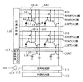
図1は、本実施の形態に係る増幅型固体撮像装置の回路構成を示す図である。
この固体撮像装置は、光を信号電荷に変換して蓄積するフォトダイオード11、フォトダイオード11の信号電荷を読み出す読み出しトランジスタ12、リセットトランジスタ13、増幅トランジスタ14、及び増幅トランジスタ14のゲートに直結するフローティングディフュージョン部(以下FD部という)15、及び垂直選択トランジスタ16からなり、信号電荷に対応する増幅信号を出力する複数の単位セル10−m・・・10−nを行列状に配置してなるイメージエリア104と、単位セル10を行単位で選択する行選択回路110と、単位セル10と接続され、信号処理部111に単位セル10の信号電圧を列単位で伝達する第1の垂直信号線109と、単位セル10の列毎に設けられ、単位セル10と信号処理部111との間の第1の垂直信号線109と接続されたバイアス電流源116と、単位セル10の列毎に設けられ、バイアス電流源116と第1の垂直信号線109との間に挿入されたカップリング制御用トランジスタ115と、カップリング制御用トランジスタ115を制御するカップリング制御回路117と、第1の垂直信号線109を介して伝達された信号電圧を保持し、ノイズをカットする信号処理部111と、単位セル10を列単位で選択する列選択回路112と、信号処理部111から出力された信号電圧を出力アンプ114に伝達する水平信号線113と、出力アンプ114とから構成される。
FIG. 1 is a diagram illustrating a circuit configuration of an amplification type solid-state imaging device according to the present embodiment.
This solid-state imaging device includes a
なお、イメージエリア104には、便宜上第1画素列及び第2画素列の2列分だけが示されている。また、各単位セル10は信号線101を介して画素電源と接続されている。
In the
カップリング制御用トランジスタ115は、CONT線をローレベルにするカップリング制御パルスの印加に対応してOFF状態となり、第1の垂直信号線109により伝達される、対応する単位セル10の列の増幅信号の信号処理部111への伝達を防止する。
The
カップリング制御回路117は、読み出しトランジスタ12による信号電荷の読み出しの開始、及び読み出しトランジスタ12による信号電荷の読み出しの終了の両方において、単位セル10の増幅信号の信号処理部111への伝達が防止されるように、カップリング制御用トランジスタ115のオン・オフを制御する。すなわち、カップリング制御回路117は、読み出しトランジスタ12による信号電荷の読み出しの開始及び終了においてカップリング制御用トランジスタ115をオフする。
The
なお、バイアス電流源116、カップリング制御用トランジスタ115及びカップリング制御回路117はそれぞれ定電圧源、第1伝達防止トランジスタ及び第1制御手段の一例であり、伝達防止手段を構成する。
The bias
以上説明したように、本発明の第1の実施の形態に係る固体撮像装置は、伝達防止手段としてカップリング制御回路117を備えていることが装置構成上の特徴である。
As described above, the solid-state imaging device according to the first embodiment of the present invention is characterized in that it includes the
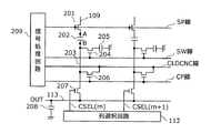
図2は、信号処理部111の回路構成を示す図である。図2では、図1に示した固体撮像装置のイメージエリア104に対応して、2列分の画素と接続された垂直信号線が示されている。
FIG. 2 is a diagram illustrating a circuit configuration of the
信号処理部111は、単位セル10とサンプリング容量205との間の信号線、つまり第1の垂直信号線109と第2の垂直信号線203との間に挿入されたサンプルホールドトランジスタ201と、サンプルホールドトランジスタ201を介して第1の垂直信号線109に接続されたクランプ容量202と、クランプ容量202を介して第1の垂直信号線109に接続された第2の垂直信号線203と、第2の垂直信号線203と接続されたサンプリングトランジスタ204と、サンプリングトランジスタ204を介して第2の垂直信号線203と接続され、第1の垂直信号線109及び第2の垂直信号線203を介して伝達される増幅信号を蓄積する蓄積素子としてのサンプリング容量205と、クランプ容量202及びサンプリングトランジスタ204に接続されたクランプトランジスタ206と、第2の垂直信号線203に接続された列選択トランジスタ207と、水平信号線113と接続された水平信号線容量208と、信号処理回路209とから構成される。
The
サンプルホールドトランジスタ201は、SP線をハイレベルにするサンプリングパルスの印加に対応して、ON状態となり、第1の垂直信号線109により伝達された信号電圧をクランプ容量202に伝達する。
The
第2の垂直信号線203は、第1の垂直信号線109からクランプ容量202を介して伝達された信号電圧を伝達する。
The second
サンプリングトランジスタ204は、SW線をハイレベルにする容量選択パルスの印加に対応して、ON状態となり、第2の垂直信号線203により伝達された信号電圧をサンプリング容量205に転送する。
The
クランプトランジスタ206は、CP線をハイレベルにするクランプパルスの印加に対応して、ON状態となり、第2の垂直信号線203と、クランプ容量202と、サンプリング容量205とをCLDCNC線の電位にリセットする。クランプ容量202はリセット時の端子A―B間の電圧を保持することで、単位セル10毎で異なる固定パターンノイズを除去する。
The
列選択トランジスタ207は、CSEL線をハイレベルにする列選択パルスの印加に対応して、順次ON状態となり、サンプリング容量205に蓄積された信号電圧を水平信号線113に転送する。
The
サンプリング容量205は、単位セル10の列毎に設けられ、対応する単位セル10の列の信号電圧を蓄積する。
The
信号処理回路209は、SP線、SW線及びCP線にパルスを印加する。
以上のような第1の実施の形態に係る固体撮像装置の動作について、図3(a)に示す駆動タイミングチャートに沿って説明する。
The
The operation of the solid-state imaging device according to the first embodiment as described above will be described along the drive timing chart shown in FIG.
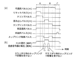
m行目の単位セル10−mが選択されると、図3(a)におけるAで示される時間領域において、LSET(m)線をハイレベルにする行選択パルス(m)が垂直選択トランジスタ16に印加され、垂直選択トランジスタ16はON状態となる。このとき、CONT線をハイレベルにするカップリング制御パルスがカップリング制御用トランジスタ115に印加されているので、増幅トランジスタ14とバイアス電流源116とでソースフォロア回路が形成され、単位セル10の画素電源に追従した電圧がソースフォロア回路から第1の垂直信号線109に出力される。
When the unit cell 10-m in the m-th row is selected, the row selection pulse (m) for setting the LSET (m) line to the high level in the time region indicated by A in FIG. And the
また、SP線をハイレベルにするサンプリングパルスがサンプルホールドトランジスタ201に印加される。サンプルホールドトランジスタ201は、ON状態となり、ソースフォロア回路から第1の垂直信号線109に出力された電圧がクランプ容量202に保持される。このとき、CP線をハイレベルにするクランプパルスがクランプトランジスタ206に印加される。クランプトランジスタ206はON状態となり、クランプ容量202の第2の垂直信号線203側がCLDCNC線の電位にリセットされる。また、同時にSW線をハイレベルにする容量選択パルスが印加されているので、サンプリングトランジスタ204はON状態となり、サンプリング容量205がCLDCNC線の電位にリセットされる。
In addition, a sampling pulse for setting the SP line to a high level is applied to the
また、RESET(m)線をハイレベルにするリセットパルス(m)がリセットトランジスタ13に印加される。リセットトランジスタ13はON状態となり、FD部15の電位がリセットされる。FD部15に接続している増幅トランジスタ14のゲート電圧はFD部15の電位となり、この電圧に応じた電圧、具体的には(FD部の電位−Vt)×αで与えられる電圧が第1の垂直信号線109に出力される。ここで、Vtは増幅トランジスタ14の閾値電圧であり、αは電圧増幅率である。
Further, a reset pulse (m) for setting the RESET (m) line to a high level is applied to the
次に、CP線をローレベルにするクランプパルスがクランプトランジスタ206に印加され、クランプトランジスタ206がOFF状態となり、第2の垂直信号線203の電位はフローティング状態となる。
Next, a clamp pulse for lowering the CP line is applied to the
次に、図3(a)におけるBで示される時間領域において、READ(m)線をハイレベルにする読み出しパルス(m)が読み出しトランジスタ12に印加される。読み出しトランジスタ12はON状態となり、フォトダイオード11に蓄積された信号電荷がFD部15に転送される。FD部15に接続している増幅トランジスタ14のゲート電圧はFD部15の電位となり、この電圧に応じた電圧、具体的には(FD部の電位−Vt)×αで与えられる電圧が第1の垂直信号線109に出力される。このとき、CP線をローレベルにするクランプパルスがクランプトランジスタ206に印加されているので、クランプトランジスタ206はOFF状態となり、サンプリング容量205には、FD部15の電位がリセットされたときに第1の垂直信号線109に出力された電圧と、フォトダイオード11に蓄積された信号電荷がFD部15に転送されたときに第1の垂直信号線109に出力された電圧との差に応じた電圧変化がm行目の単位セル10−mの信号電圧として蓄積される。
Next, in the time region indicated by B in FIG. 3A, a read pulse (m) that sets the READ (m) line to a high level is applied to the
ここで、読み出しトランジスタ12がOFF状態からON状態に変化する場合(図3におけるt1)及びON状態からOFF状態に変化する場合(図3におけるt2)において、カップリング制御パルスをローレベルにしてカップリング制御トランジスタ115を一時的にOFF状態にする。よって、図3(b)に示されるように、読み出しトランジスタ12がOFF状態からON状態に変化する時に、読み出しトランジスタ12のゲートとソース間の寄生容量を介して起こるFD部15への電圧カップリングの影響は第1の垂直信号線109に伝達されるが、第2の垂直信号線203には伝達されない。また、読み出しトランジスタ12がON状態からOFF状態に変化する時に、読み出しトランジスタ12のゲートとソース間の寄生容量を介して起こるFD部15への電圧カップリングの影響についても第1の垂直信号線109に伝達されるが、第2の垂直信号線203に伝達されない。
Here, when the
次に、図3(a)におけるCで示される時間領域において、CSEL(m)線をハイレベルにする列選択パルス(m)、CSEL(m+1)線をハイレベルにする列選択パルス(m−1)、・・・が列選択トランジスタ207に順次印加され、各列選択トランジスタ207は順次ON状態となり、サンプリング容量205に蓄積された信号電圧が水平信号線113に順次出力される。
Next, in the time domain indicated by C in FIG. 3A, the column selection pulse (m) for setting the CSEL (m) line to the high level and the column selection pulse (m−) for setting the CSEL (m + 1) line to the high level. 1),... Are sequentially applied to the
以上のように本実施の形態に係る固体撮像装置によれば、読み出しトランジスタ12がOFF状態からON状態になる場合及びON状態からOFF状態になる場合において、一時的にカップリング制御パルスをローレベルにする事で、カップリング制御用トランジスタ108がOFF状態にされる。よって、読み出しトランジスタ12のゲートの電圧変化がソースとゲート間の容量を介してFD部15にカップリングし、FD部15の電位が変化し、FD部15のソースフォロワを介して電位変化が第2の垂直信号線203に伝達することを抑制できる。すなわち、FD部15のカップリングの影響が第2の垂直信号線203に伝達されるのを抑制し、各列におけるFD部15のカップリングばらつきが第2の垂直信号線203に影響するのを抑制できるので、カップリングに起因する画像不良を抑制できる。また、垂直信号線上にアンプ等の増幅機能をつけて信号成分を増幅することにより低ノイズ化を図る場合においても、カップリングの影響は伝達しないため、フォトダイオードからの信号の増幅率を従来よりも大きくでき、低ノイズ化に大きく貢献できる。
As described above, according to the solid-state imaging device according to the present embodiment, when the
なお、本実施の形態の固体撮像装置において、読み出しトランジスタ12による信号電荷の読み出しの開始、及び読み出しトランジスタ12による信号電荷の読み出しの終了の両方において、単位セル10の増幅信号の信号処理部111への伝達が防止されるように、カップリング制御用トランジスタ115のオン・オフを制御するとした。しかし、読み出しトランジスタ12による信号電荷の読み出しの開始及び終了のいずれかにおいて、単位セル10の増幅信号の信号処理部111への伝達が防止されるように、カップリング制御用トランジスタ115のオン・オフを制御してもよい。
In the solid-state imaging device of the present embodiment, the
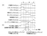
すなわち、図4(a)に示されるように、読み出しトランジスタ12がOFF状態からON状態になる場合においてのみ、一時的にカップリング制御パルスをローレベルにする事で、カップリング制御用トランジスタ115をOFF状態にしてもよい。これによって、図4(b)に示されるように、読み出しトランジスタ12がOFF状態からON状態になる場合において、FD部15のカップリングの影響が第2の垂直信号線203に伝達されるのを抑制し、FD部15のカップリングばらつきが第2の垂直信号線203に影響するのを抑制できるので、カップリングに起因する画像不良を抑制できる。
That is, as shown in FIG. 4A, only when the
また、図5(a)に示されるように、読み出しトランジスタ12がON状態からOFF状態になる場合においてのみ、一時的にカップリング制御パルスをローレベルにする事で、カップリング制御用トランジスタ115をOFF状態にしてもよい。これによって、図5(b)に示されるように、読み出しトランジスタ12がON状態からOFF状態になる場合において、FD部15のカップリングの影響が第2の垂直信号線203に伝達されるのを抑制し、FD部15のカップリングばらつきが第2の垂直信号線203に影響するのを抑制できるので、カップリングに起因する画像不良を抑制できる。
Further, as shown in FIG. 5A, only when the
また、本実施の形態の固体撮像装置において、カップリング制御用トランジスタ115はイメージエリア104と信号処理部111との間の第1の垂直信号線109に設けられるとしたが、これに限られず、第1の垂直信号線109上のどこに設けてもよい。
In the solid-state imaging device according to the present embodiment, the
(第2の実施形態)
以下、本発明の第2の実施の形態に係る固体撮像装置及びその駆動方法について、第1の実施の形態の固体撮像装置と異なる点を中心に、図面を参照しながら説明する。
(Second Embodiment)
Hereinafter, a solid-state imaging device and a driving method thereof according to a second embodiment of the present invention will be described with reference to the drawings, focusing on differences from the solid-state imaging device of the first embodiment.
図6は、第2の実施の形態に係る増幅型固体撮像装置の回路構成を示す図である。
この固体撮像装置は、カップリング制御用トランジスタではなくサンプルホールドトランジスタを制御することで、読み出しトランジスタによる信号電荷の読み出しの開始、及び読み出しトランジスタによる信号電荷の読み出しの終了における、単位セルの増幅信号のサンプリング容量への伝達を防止するという点で第1の実施の形態の固体撮像装置と異なる。
FIG. 6 is a diagram illustrating a circuit configuration of the amplification type solid-state imaging device according to the second embodiment.
This solid-state imaging device controls the sample hold transistor, not the coupling control transistor, so that the unit cell amplification signal at the start of signal charge readout by the read transistor and at the end of signal charge read by the read transistor is It differs from the solid-state imaging device of the first embodiment in that transmission to the sampling capacitor is prevented.
この固体撮像装置は、複数の単位セル10−m・・・10−nを行列状に配置してなるイメージエリア104と、行選択回路110と、第1の垂直信号線109と、第1の垂直信号線109を介して伝達された信号電圧を保持し、ノイズをカットする信号処理部311と、列選択回路112と、水平信号線113と、出力アンプ114と、負荷トランジスタ群315とから構成される。
This solid-state imaging device includes an
図7は、信号処理部311の回路構成を示す図である。図7では、図6に示した固体撮像装置のイメージエリア104に対応して、2列分の画素と接続された垂直信号線が示されている。
FIG. 7 is a diagram illustrating a circuit configuration of the
信号処理部311は、単位セル10の列毎に設けられ、単位セル10とサンプリング容量205との間の信号線、つまり第1の垂直信号線109と第2の垂直信号線203との間に挿入されたサンプルホールドトランジスタ401と、クランプ容量202と、第2の垂直信号線203と、サンプリングトランジスタ204と、サンプリング容量205と、クランプトランジスタ206と、列選択トランジスタ207と、水平信号線容量208と、信号処理回路409とから構成される。
The
サンプルホールドトランジスタ401は、SP線をハイレベルにするサンプリングパルスの印加に対応して、ON状態となり、第1の垂直信号線109により伝達された信号電圧をクランプ容量202に伝達する。また、SP線をローレベルにするサンプリングパルスの印加に対応してOFF状態となり、第1の垂直信号線109により伝達される、対応する単位セル10の列の増幅信号のサンプリング容量205への伝達を防止する。
The
信号処理回路409は、SP線、SW線及びCP線にパルスを印加する。また、読み出しトランジスタ12による信号電荷の読み出しの開始、及び読み出しトランジスタ12による信号電荷の読み出しの終了の両方において、単位セル10の増幅信号のサンプリング容量205への伝達が防止されるように、サンプルホールドトランジスタ401のオン・オフを制御する。すなわち、信号処理回路409は、読み出しトランジスタ12による信号電荷の読み出しの開始及び終了においてサンプルホールドトランジスタ401をオフする。
The
なお、サンプルホールドトランジスタ401及び信号処理回路409はそれぞれ第2伝達防止トランジスタ及び第2制御手段の一例であり、伝達防止手段を構成する。
The
以上説明したように、本発明の第2の実施の形態に係る固体撮像装置は、伝達防止手段としてサンプルホールドトランジスタ401に接続した信号処理回路409を備えていることが装置構成上の特徴である。
As described above, the solid-state imaging device according to the second embodiment of the present invention is characterized in that it includes the
以上のような第2の実施の形態に係る固体撮像装置の動作について、図3(a)に示す駆動タイミングチャートに沿って説明する。 The operation of the solid-state imaging device according to the second embodiment as described above will be described along the drive timing chart shown in FIG.
m行目の単位セル10−mが選択されると、図8(a)におけるAで示される時間領域において、LSET(m)線をハイレベルにする行選択パルス(m)が垂直選択トランジスタ16に印加される。垂直選択トランジスタ16はON状態となり、増幅トランジスタ14と負荷トランジスタ群315とでソースフォロア回路が形成され、単位セル10の画素電源に追従した電圧がソースフォロア回路から第1の垂直信号線109に出力される。
When the unit cell 10-m in the m-th row is selected, the row selection pulse (m) for setting the LSET (m) line to the high level in the time domain indicated by A in FIG. To be applied. The
また、SP線をハイレベルにするサンプリングパルスがサンプルホールドトランジスタ401に印加される。サンプルホールドトランジスタ401は、ON状態となり、ソースフォロア回路から第1の垂直信号線109に出力された電圧がクランプ容量202に保持される。このとき、CP線をハイレベルにするクランプパルスがクランプトランジスタ206に印加される。クランプトランジスタ206はON状態となり、クランプ容量202の第2の垂直信号線203側がCLDCNC線の電位にリセットされる。また、同時にSW線をハイレベルにする容量選択パルスが印加されているので、サンプリングトランジスタ204はON状態となり、サンプリング容量205がCLDCNC線の電位にリセットされる。
A sampling pulse for setting the SP line to a high level is applied to the
また、RESET(m)線をハイレベルにするリセットパルス(m)がリセットトランジスタ13に印加される。リセットトランジスタ13はON状態となり、FD部15の電位がリセットされる。FD部15に接続している増幅トランジスタ14のゲート電圧はFD部15の電位となり、この電圧に応じた電圧が第1の垂直信号線109に出力される。
Further, a reset pulse (m) for setting the RESET (m) line to a high level is applied to the
次に、CP線をローレベルにするクランプパルスがクランプトランジスタ206に印加され、クランプトランジスタ206がOFF状態となり、第2の垂直信号線203の電位はフローティング状態となる。
Next, a clamp pulse for lowering the CP line is applied to the
次に、図8(a)におけるBで示される時間領域において、READ(m)線をハイレベルにする読み出しパルス(m)が読み出しトランジスタ12に印加される。読み出しトランジスタ12はON状態となり、フォトダイオード11に蓄積された信号電荷がFD部15に転送される。FD部15に接続している増幅トランジスタ14のゲート電圧はFD部15の電位となり、この電圧に応じた電圧が第1の垂直信号線109に出力される。このとき、CP線をローレベルにするクランプパルスがクランプトランジスタ206に印加されているので、クランプトランジスタ206はOFF状態となり、サンプリング容量205には、FD部15の電位がリセットされたときに第1の垂直信号線109に出力された電圧と、フォトダイオード11に蓄積された信号電荷がFD部15に転送されたときに第1の垂直信号線109に出力された電圧との差に応じた電圧変化がm行目の単位セル10−mの信号電圧として蓄積される。
Next, in the time region indicated by B in FIG. 8A, a read pulse (m) that sets the READ (m) line to a high level is applied to the
ここで、読み出しトランジスタ12がOFF状態からON状態に変化する場合(図8におけるt1)及びON状態からOFF状態に変化する場合(図8におけるt2)において、サンリングパルスをローレベルにしてサンプルホールドトランジスタ401を一時的にOFF状態にする。よって、図8(b)に示されるように、読み出しトランジスタ12がOFF状態からON状態に変化する時に、読み出しトランジスタ12のゲートとソース間の寄生容量を介して起こるFD部15への電圧カップリングの影響は第1の垂直信号線109に伝達されるが、第2の垂直信号線203には伝達されない。また、読み出しトランジスタ12がON状態からOFF状態に変化する時に、読み出しトランジスタ12のゲートとソース間の寄生容量を介して起こるFD部15への電圧カップリングの影響についても第1の垂直信号線109に伝達されるが、第2の垂直信号線203に伝達されない。
Here, when the reading
次に、図8(a)におけるCで示される時間領域において、CSEL(m)線をハイレベルにする列選択パルス(m)、CSEL(m+1)線をハイレベルにする列選択パルス(m−1)、・・・が列選択トランジスタ207に順次印加され、各列選択トランジスタ207は順次ON状態となり、サンプリング容量205に蓄積された信号電圧が水平信号線113に順次出力される。
Next, in the time domain indicated by C in FIG. 8A, the column selection pulse (m) for setting the CSEL (m) line to the high level and the column selection pulse (m−) for setting the CSEL (m + 1) line to the high level. 1),... Are sequentially applied to the
以上のように本実施の形態に係る固体撮像装置によれば、読み出しトランジスタ12がOFF状態からON状態になる場合及びON状態からOFF状態になる場合において、一時的にサンプリングパルスをローレベルにする事で、サンプルホールドトランジスタ401がOFF状態にされる。よって、読み出しトランジスタ12のゲートの電圧変化がソースとゲート間の容量を介してFD部15にカップリングし、FD部15の電位が変化し、FD部15のソースフォロワを介して電位変化が第2の垂直信号線203に伝達することを抑制できる。すなわち、各列におけるFD部15のカップリングの影響が第2の垂直信号線203に伝達するのを抑制し、FD部15のカップリングばらつきが第2の垂直信号線203に影響するのを抑制できるのでカップリングに起因する画像不良を抑制できる。
As described above, according to the solid-state imaging device according to the present embodiment, the sampling pulse is temporarily set to the low level when the
また、本実施の形態に係る固体撮像装置によれば、第1の実施の形態の固体撮像装置のように、FD部15のカップリングの影響が第2の垂直信号線203に伝達するのを抑制するための新たなトランジスタを設ける必要がないので、低コストかつ高性能の固体撮像装置を実現できる。
Further, according to the solid-state imaging device according to the present embodiment, the influence of the coupling of the
なお、本実施の形態の固体撮像装置において、読み出しトランジスタ12による信号電荷の読み出しの開始、及び読み出しトランジスタ12による信号電荷の読み出しの終了の両方において、単位セル10の増幅信号のサンプリング容量205への伝達が防止されるように、サンプルホールドトランジスタ401のオン・オフを制御するとした。しかし、読み出しトランジスタ12による信号電荷の読み出しの開始及び終了のいずれかにおいて、単位セル10の増幅信号のサンプリング容量205への伝達が防止されるように、サンプルホールドトランジスタ401のオン・オフを制御してもよい。
In the solid-state imaging device of the present embodiment, the amplified signal of the
すなわち、図9(a)に示されるように、読み出しトランジスタ12がOFF状態からON状態になる場合においてのみ、一時的にサンプリングパルスをローレベルにする事で、サンプルホールドトランジスタ401をOFF状態にしてもよい。これによって、図9(b)に示されるように、読み出しトランジスタ12がOFF状態からON状態になる場合において、FD部15のカップリングの影響が第2の垂直信号線203に伝達されるのを抑制し、FD部15のカップリングばらつきが第2の垂直信号線203に影響するのを抑制できるので、カップリングに起因する画像不良を抑制できる。
That is, as shown in FIG. 9A, only when the
また、図10(a)に示されるように、読み出しトランジスタ12がON状態からOFF状態になる場合においてのみ、一時的にサンプリングパルスをローレベルにする事で、サンプルホールドトランジスタ401をOFF状態にしてもよい。これによって、図10(b)に示されるように、読み出しトランジスタ12がON状態からOFF状態になる場合において、FD部15のカップリングの影響が第2の垂直信号線203に伝達されるのを抑制し、FD部15のカップリングばらつきが第2の垂直信号線203に影響するのを抑制できるので、カップリングに起因する画像不良を抑制できる。
Further, as shown in FIG. 10A, only when the
(第3の実施の形態)
以下、本発明の第3の実施の形態に係るカメラについて、図面を参照しながら説明する。
(Third embodiment)
Hereinafter, a camera according to a third embodiment of the present invention will be described with reference to the drawings.
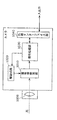
図11は、第3の実施の形態に係るカメラのブロック図である。
このカメラは、第1及び第2の実施の形態の増幅型固体撮像装置1010を用いたカメラであって、レンズ1000と、固体撮像装置1010と、駆動回路1020と、信号処理部1030と、外部インターフェイス部1040とからなる。
FIG. 11 is a block diagram of a camera according to the third embodiment.
This camera is a camera using the amplification type solid-
上記構成を有するカメラにおいて、外部に信号が出力されるまでの処理は以下のような順序に沿っておこなわれる。
(1)レンズ1000を光が通過し、固体撮像装置1010に入る。
(2)信号処理部1030は、駆動回路1020を通して固体撮像装置1010を駆動し、固体撮像装置1010からの出力信号を取り込む。
(3)信号処理部1030で処理した信号を、外部インターフェイス部1040を通して外部に出力する。
In the camera having the above configuration, processing until a signal is output to the outside is performed in the following order.
(1) Light passes through the
(2) The
(3) The signal processed by the
以上のように本実施の形態のカメラによれば、カップリングに起因する画像不良を抑制することが可能な固体撮像装置を備えたカメラを実現できる。よって、画質に優れたカメラを実現することができる。 As described above, according to the camera of the present embodiment, it is possible to realize a camera including a solid-state imaging device capable of suppressing image defects caused by coupling. Therefore, a camera with excellent image quality can be realized.
以上、本発明の固体撮像装置及びその駆動方法について、実施の形態に基づいて説明したが、本発明は、この実施の形態の限定されるものではない。本発明の要旨を逸脱しない範囲内で当業者が思いつく各種変形を施したものも本発明の範囲内に含まれる。 As described above, the solid-state imaging device and the driving method thereof according to the present invention have been described based on the embodiment. However, the present invention is not limited to this embodiment. The present invention includes various modifications made by those skilled in the art without departing from the scope of the present invention.
例えば、固体撮像装置の駆動タイミングは、第1の実施の形態及び第2の実施の形態で示した駆動タイミングを組み合わせたものであっても構わない。 For example, the drive timing of the solid-state imaging device may be a combination of the drive timings shown in the first embodiment and the second embodiment.
本発明は、固体撮像装置その駆動方法に利用でき、特に増幅型固体撮像装置及びその駆動方法等に利用することができる。 The present invention can be used for a solid-state imaging device and a driving method thereof, and in particular, an amplification type solid-state imaging device and a driving method thereof.
10、20 単位セル
11、21 フォトダイオード
12、22 読み出しトランジスタ
13、23 リセットトランジスタ
14、24 増幅トランジスタ
15、25 フローティングディフュージョン部
104、504 イメージエリア
109、509 第1の垂直信号線
110、510 行選択回路
111、311、511、1030 信号処理部
112、512 列選択回路
113、513 水平信号線
114、514 出力アンプ
115 カップリング制御用トランジスタ
116 バイアス電流源
117 カップリング制御回路
201、401、601 サンプルホールドトランジスタ
202、602 クランプ容量
203、603 第2の垂直信号線
204、604 サンプリングトランジスタ
205、605 サンプリング容量
206、606 クランプトランジスタ
207、607 列選択トランジスタ
208、608 水平信号線容量
315、515 負荷トランジスタ群
209、409 信号処理回路
1000 レンズ
1010 固体撮像装置
1020 駆動回路
1040 外部インターフェイス
10, 20
Claims (9)
光を信号電荷に変換して蓄積するフォトダイオードと、前記フォトダイオードの信号電荷を読み出す読み出しトランジスタとを有し、信号電荷に対応する増幅信号を出力する単位セルと、
前記単位セルと接続された信号線と、
前記信号線を介して伝達される前記増幅信号を蓄積する蓄積素子と、
前記読み出しトランジスタによる前記信号電荷の読み出しの開始、及び前記読み出しトランジスタによる前記信号電荷の読み出しの終了のいずれかにおいて、前記単位セルの増幅信号の前記蓄積素子への伝達を防止する伝達防止手段とを備える
ことを特徴とする固体撮像装置。 An amplification type solid-state imaging device,
A unit cell that outputs a amplified signal corresponding to the signal charge, including a photodiode that converts light into signal charge and accumulates, and a read transistor that reads the signal charge of the photodiode;
A signal line connected to the unit cell;
A storage element for storing the amplified signal transmitted through the signal line;
Transmission preventing means for preventing transmission of the amplified signal of the unit cell to the storage element at any one of the start of reading of the signal charge by the read transistor and the end of reading of the signal charge by the read transistor; A solid-state imaging device.
ことを特徴とする請求項1記載の固体撮像装置。 The transmission preventing means is a second transmission preventing transistor inserted in the signal line between the unit cell and the storage element, and second control means for controlling the second transmission transistor. The solid-state imaging device according to claim 1.
ことを特徴とする請求項1記載の固体撮像装置。 The transmission preventing means includes a constant voltage source connected to a signal line between the unit cell and the storage element, a first transmission preventing transistor inserted between the constant voltage source and the signal line, The solid-state imaging device according to claim 1, wherein the solid-state imaging device is a first control unit that controls the first transmission preventing transistor.
前記単位セルと接続された信号線と、
前記信号線を介して伝達される前記増幅信号を蓄積する蓄積素子と、
前記単位セルと前記蓄積素子との間の前記信号線に挿入された第2伝達防止トランジスタと、
前記第2伝達トランジスタを制御する第2制御手段とを備える増幅型固体撮像装置の駆動方法であって、
前記第2制御手段は、前記読み出しトランジスタによる前記信号電荷の読み出しの開始、及び前記読み出しトランジスタによる前記信号電荷の読み出しの終了のいずれかにおいて、前記第2伝達防止トランジスタがオフ状態になるように制御する
ことを特徴とする固体撮像装置の駆動方法。 A unit cell that outputs a amplified signal corresponding to the signal charge, including a photodiode that converts light into signal charge and accumulates, and a read transistor that reads the signal charge of the photodiode;
A signal line connected to the unit cell;
A storage element for storing the amplified signal transmitted through the signal line;
A second transmission preventing transistor inserted in the signal line between the unit cell and the storage element;
A method of driving an amplification type solid-state imaging device comprising: a second control unit that controls the second transmission transistor,
The second control unit controls the second transmission preventing transistor to be in an off state at any one of the start of reading of the signal charge by the read transistor and the end of reading of the signal charge by the read transistor. A method for driving a solid-state imaging device.
前記蓄積素子は、前記単位セルの列毎に設けられ、対応する前記単位セルの列の増幅信号を蓄積し、
前記第2伝達防止トランジスタは、前記単位セルの列毎に設けられ、
前記第2制御手段は、所定の列の単位セルにおいて前記信号電荷の読み出しが行われるときには、前記所定の列の単位セルに対応して設けられた前記第2伝達防止トランジスタを制御する
ことを特徴とする請求項4記載の固体撮像装置の駆動方法。 A plurality of the unit cells are arranged in a matrix,
The storage element is provided for each column of the unit cells, and stores the amplified signal of the corresponding column of the unit cells,
The second transmission preventing transistor is provided for each column of the unit cells,
The second control means controls the second transmission preventing transistor provided corresponding to the unit cell of the predetermined column when the signal charge is read in the unit cell of the predetermined column. The driving method of the solid-state imaging device according to claim 4.
前記単位セルと接続された信号線と、
前記信号線を介して伝達される前記増幅信号を蓄積する蓄積素子と、
前記単位セルと前記蓄積素子との間の信号線に接続された定電圧源と、
前記定電圧源と前記信号線との間に挿入された第1伝達防止トランジスタと、
前記第1伝達防止トランジスタを制御する第1制御手段とを備える増幅型固体撮像装置の駆動方法であって、
前記第1制御手段は、前記読み出しトランジスタによる前記信号電荷の読み出しの開始、及び前記読み出しトランジスタによる前記信号電荷の読み出しの終了のいずれかにおいて、前記第1伝達防止トランジスタがオフ状態になるように制御する
ことを特徴とする固体撮像装置の駆動方法。 A unit cell that outputs a amplified signal corresponding to the signal charge, including a photodiode that converts light into signal charge and accumulates, and a read transistor that reads the signal charge of the photodiode;
A signal line connected to the unit cell;
A storage element for storing the amplified signal transmitted through the signal line;
A constant voltage source connected to a signal line between the unit cell and the storage element;
A first transmission preventing transistor inserted between the constant voltage source and the signal line;
A method for driving an amplification type solid-state imaging device comprising: a first control unit that controls the first transmission preventing transistor,
The first control unit controls the first transmission preventing transistor to be in an off state at one of the start of reading of the signal charge by the read transistor and the end of reading of the signal charge by the read transistor. A method for driving a solid-state imaging device.
前記蓄積素子は、前記単位セルの列毎に設けられ、対応する前記単位セルの列の増幅信号を蓄積し、
前記第1伝達防止トランジスタは、前記単位セルの列毎に設けられ、
前記第1制御手段は、所定の列の単位セルにおいて前記信号電荷の読み出しが行われるときには、前記所定の列の単位セルに対応して設けられた前記第1伝達防止トランジスタを制御する
ことを特徴とする請求項6記載の固体撮像装置の駆動方法。 A plurality of the unit cells are arranged in a matrix,
The storage element is provided for each column of the unit cells, and stores the amplified signal of the corresponding column of the unit cells,
The first transmission preventing transistor is provided for each column of the unit cells,
The first control unit controls the first transmission preventing transistor provided corresponding to the unit cell of the predetermined column when the signal charge is read in the unit cell of the predetermined column. The method for driving a solid-state imaging device according to claim 6.
ことを特徴とする請求項4又は6記載の固体撮像装置の駆動方法。 The first control unit or the second control unit is configured to store the amplification signal of the unit cell at both the start of reading of the signal charge by the read transistor and the end of reading of the signal charge by the read transistor. The method for driving a solid-state imaging device according to claim 4, wherein transmission to the device is prevented.
前記信号処理部は、前記駆動回路を通して前記固体撮像装置を駆動し、前記固体撮像装置からの出力信号を取り込んで処理し、前記処理した信号を外部に出力する
ことを特徴とするカメラ。 The solid-state imaging device according to claim 1, a signal processing unit, and a drive circuit,
The camera, wherein the signal processing unit drives the solid-state imaging device through the drive circuit, takes in and processes an output signal from the solid-state imaging device, and outputs the processed signal to the outside.
Priority Applications (3)
| Application Number | Priority Date | Filing Date | Title |
|---|---|---|---|
| JP2005360898A JP4328327B2 (en) | 2005-12-14 | 2005-12-14 | Solid-state imaging device and driving method thereof |
| US11/610,007 US7924331B2 (en) | 2005-12-14 | 2006-12-13 | Solid-state imaging device and driving method thereof that prevents image quality defect caused by coupling occuring when signal charge is read out from photodiode |
| KR1020060127666A KR20070063451A (en) | 2005-12-14 | 2006-12-14 | Solid state imaging device and driving method thereof |
Applications Claiming Priority (1)
| Application Number | Priority Date | Filing Date | Title |
|---|---|---|---|
| JP2005360898A JP4328327B2 (en) | 2005-12-14 | 2005-12-14 | Solid-state imaging device and driving method thereof |
Publications (2)
| Publication Number | Publication Date |
|---|---|
| JP2007166320A true JP2007166320A (en) | 2007-06-28 |
| JP4328327B2 JP4328327B2 (en) | 2009-09-09 |
Family
ID=38193147
Family Applications (1)
| Application Number | Title | Priority Date | Filing Date |
|---|---|---|---|
| JP2005360898A Expired - Lifetime JP4328327B2 (en) | 2005-12-14 | 2005-12-14 | Solid-state imaging device and driving method thereof |
Country Status (3)
| Country | Link |
|---|---|
| US (1) | US7924331B2 (en) |
| JP (1) | JP4328327B2 (en) |
| KR (1) | KR20070063451A (en) |
Cited By (1)
| Publication number | Priority date | Publication date | Assignee | Title |
|---|---|---|---|---|
| WO2013179597A1 (en) * | 2012-05-30 | 2013-12-05 | パナソニック株式会社 | Solid-state imaging device, method for driving same, and image-capturing device |
Families Citing this family (7)
| Publication number | Priority date | Publication date | Assignee | Title |
|---|---|---|---|---|
| WO2006090633A1 (en) * | 2005-02-23 | 2006-08-31 | Matsushita Electric Industrial Co., Ltd. | Mos type solid-state image pickup device, method for driving such mos type solid-state image pickup device, and camera |
| JP2008004682A (en) * | 2006-06-21 | 2008-01-10 | Matsushita Electric Ind Co Ltd | Solid-state imaging device, driving method and manufacturing method thereof |
| JP5173171B2 (en) * | 2006-09-07 | 2013-03-27 | キヤノン株式会社 | PHOTOELECTRIC CONVERSION DEVICE, IMAGING DEVICE, AND SIGNAL READING METHOD |
| JP2009038531A (en) * | 2007-07-31 | 2009-02-19 | Panasonic Corp | Solid-state imaging device and driving method thereof |
| JP2009177797A (en) * | 2007-12-26 | 2009-08-06 | Panasonic Corp | Solid-state imaging device and driving method thereof |
| JP5258416B2 (en) * | 2008-06-27 | 2013-08-07 | パナソニック株式会社 | Solid-state imaging device |
| KR101022118B1 (en) * | 2009-09-02 | 2011-03-17 | 삼성모바일디스플레이주식회사 | Optical sensing circuit and its driving method and touch screen panel having same |
Family Cites Families (9)
| Publication number | Priority date | Publication date | Assignee | Title |
|---|---|---|---|---|
| JPH07321299A (en) | 1994-05-25 | 1995-12-08 | Fuji Xerox Co Ltd | Integrated circuits and thin film integrated circuits |
| JP3667186B2 (en) | 2000-02-29 | 2005-07-06 | キヤノン株式会社 | Signal transfer device and solid-state imaging device using the same |
| KR100397663B1 (en) * | 2000-06-23 | 2003-09-13 | (주) 픽셀플러스 | Cmos image sensor in which dataline is maintained as data of reset mode |
| JP3801112B2 (en) | 2002-07-26 | 2006-07-26 | 富士ゼロックス株式会社 | Image reading signal processing apparatus |
| JP2004080410A (en) | 2002-08-19 | 2004-03-11 | Toshiba Corp | Flat panel detector and radiation diagnostic apparatus including flat panel detector |
| JP3562649B1 (en) | 2003-03-20 | 2004-09-08 | 松下電器産業株式会社 | Solid-state imaging device and driving method thereof |
| JP4339151B2 (en) | 2004-03-04 | 2009-10-07 | シャープ株式会社 | Photoelectric conversion device |
| JP2005348041A (en) * | 2004-06-02 | 2005-12-15 | Canon Inc | Solid-state imaging device and imaging system |
| US20060208158A1 (en) * | 2005-02-28 | 2006-09-21 | Matsushita Electric Industrial Co. Ltd. | Solid-state image device, driving method thereof, and camera |
-
2005
- 2005-12-14 JP JP2005360898A patent/JP4328327B2/en not_active Expired - Lifetime
-
2006
- 2006-12-13 US US11/610,007 patent/US7924331B2/en active Active
- 2006-12-14 KR KR1020060127666A patent/KR20070063451A/en not_active Withdrawn
Cited By (2)
| Publication number | Priority date | Publication date | Assignee | Title |
|---|---|---|---|---|
| WO2013179597A1 (en) * | 2012-05-30 | 2013-12-05 | パナソニック株式会社 | Solid-state imaging device, method for driving same, and image-capturing device |
| US9419052B2 (en) | 2012-05-30 | 2016-08-16 | Panasonic Intellectual Property Management Co., Ltd. | Solid-state imaging apparatus, method for driving the same, and imaging apparatus |
Also Published As
| Publication number | Publication date |
|---|---|
| US7924331B2 (en) | 2011-04-12 |
| JP4328327B2 (en) | 2009-09-09 |
| KR20070063451A (en) | 2007-06-19 |
| US20070146516A1 (en) | 2007-06-28 |
Similar Documents
| Publication | Publication Date | Title |
|---|---|---|
| US7561199B2 (en) | Solid-state image pickup device | |
| JP4804254B2 (en) | Photoelectric conversion device and imaging device | |
| KR101027664B1 (en) | Solid-state imaging devices and electronic information equipment | |
| KR101900668B1 (en) | Solid-state imaging element, and imaging device | |
| JP6172608B2 (en) | Solid-state imaging device, driving method thereof, and imaging device | |
| US20060262209A1 (en) | Image sensing device and control method therefor | |
| US11240448B2 (en) | Solid-state imaging device, method for driving solid-state imaging device, and electronic apparatus | |
| JP5173503B2 (en) | Imaging apparatus and imaging system | |
| JP2008042679A (en) | Photoelectric conversion device and imaging device | |
| JP6037178B2 (en) | Solid-state imaging device and imaging device | |
| US20130250151A1 (en) | Solid-state imaging device | |
| US20140002703A1 (en) | Solid state imaging element and camera system | |
| JP4328327B2 (en) | Solid-state imaging device and driving method thereof | |
| JP2012160848A (en) | Imaging apparatus, imaging system, and driving method of imaging apparatus | |
| KR100842513B1 (en) | Solid-state image pickup device | |
| JP2006186467A (en) | Physical information acquisition method and physical information acquisition device | |
| JP4807014B2 (en) | Solid-state imaging device, driving method of solid-state imaging device, and imaging device | |
| JP2009302978A (en) | Solid-state imaging apparatus and control method thereof, and electronic information device | |
| JP4959624B2 (en) | Solid-state imaging device and electronic information device | |
| JP5177198B2 (en) | Physical information acquisition method and physical information acquisition device | |
| JP2008042674A (en) | Solid-state imaging device | |
| JP4453306B2 (en) | Solid-state image sensor and driving method of solid-state image sensor | |
| JP4347820B2 (en) | Imaging device | |
| JP2008079001A (en) | Solid-state imaging device | |
| JP2008042675A (en) | Photoelectric conversion device and imaging device |
Legal Events
| Date | Code | Title | Description |
|---|---|---|---|
| A977 | Report on retrieval |
Free format text: JAPANESE INTERMEDIATE CODE: A971007 Effective date: 20090416 |
|
| TRDD | Decision of grant or rejection written | ||
| A01 | Written decision to grant a patent or to grant a registration (utility model) |
Free format text: JAPANESE INTERMEDIATE CODE: A01 Effective date: 20090519 |
|
| A01 | Written decision to grant a patent or to grant a registration (utility model) |
Free format text: JAPANESE INTERMEDIATE CODE: A01 |
|
| A61 | First payment of annual fees (during grant procedure) |
Free format text: JAPANESE INTERMEDIATE CODE: A61 Effective date: 20090612 |
|
| FPAY | Renewal fee payment (event date is renewal date of database) |
Free format text: PAYMENT UNTIL: 20120619 Year of fee payment: 3 |
|
| R150 | Certificate of patent or registration of utility model |
Ref document number: 4328327 Country of ref document: JP Free format text: JAPANESE INTERMEDIATE CODE: R150 Free format text: JAPANESE INTERMEDIATE CODE: R150 |
|
| FPAY | Renewal fee payment (event date is renewal date of database) |
Free format text: PAYMENT UNTIL: 20120619 Year of fee payment: 3 |
|
| FPAY | Renewal fee payment (event date is renewal date of database) |
Free format text: PAYMENT UNTIL: 20130619 Year of fee payment: 4 |
|
| S111 | Request for change of ownership or part of ownership |
Free format text: JAPANESE INTERMEDIATE CODE: R313113 |
|
| R350 | Written notification of registration of transfer |
Free format text: JAPANESE INTERMEDIATE CODE: R350 |
|
| R250 | Receipt of annual fees |
Free format text: JAPANESE INTERMEDIATE CODE: R250 |
|
| R250 | Receipt of annual fees |
Free format text: JAPANESE INTERMEDIATE CODE: R250 |
|
| R250 | Receipt of annual fees |
Free format text: JAPANESE INTERMEDIATE CODE: R250 |
|
| R250 | Receipt of annual fees |
Free format text: JAPANESE INTERMEDIATE CODE: R250 |
|
| R250 | Receipt of annual fees |
Free format text: JAPANESE INTERMEDIATE CODE: R250 |
|
| EXPY | Cancellation because of completion of term |