JP2007165651A - Recess formation method and electronic device - Google Patents
Recess formation method and electronic device Download PDFInfo
- Publication number
- JP2007165651A JP2007165651A JP2005360858A JP2005360858A JP2007165651A JP 2007165651 A JP2007165651 A JP 2007165651A JP 2005360858 A JP2005360858 A JP 2005360858A JP 2005360858 A JP2005360858 A JP 2005360858A JP 2007165651 A JP2007165651 A JP 2007165651A
- Authority
- JP
- Japan
- Prior art keywords
- recess
- resist film
- forming
- substrate
- solid phase
- Prior art date
- Legal status (The legal status is an assumption and is not a legal conclusion. Google has not performed a legal analysis and makes no representation as to the accuracy of the status listed.)
- Pending
Links
Images


Abstract
Description
本発明は、基板等の固相表面に内壁が階段上になった凹部を形成する方法等に関する。 The present invention relates to a method of forming a recess having an inner wall on a solid surface such as a substrate.
液滴吐出ヘッド等のマイクロデバイスは、配線や電極等の構成要素、凹部、貫通孔等が形成された複数の基板を貼り合わせることによって構成されているものも多い。 Many micro devices such as a droplet discharge head are configured by bonding together a plurality of substrates on which components such as wiring and electrodes, concave portions, through holes, and the like are formed.
特開2005−153369(特許文献1)等にも開示されている通り、基板に凹部を形成する際は、単に1つのマスクの開口にあわせて円筒状の凹部を設けるだけでなく、種々のキャビティ、位置決め用基準孔、基板同士を貼り合わせるときの接着剤逃げ等のため、内壁が多段状になっている凹部を形成することが必要な場合がある。内壁が多段状になっている凹部は、エッチング法によって、まず一番直径が小さく深い凹部を形成し、続いてその凹部の開口部より直径の大きいマスクを使用してより浅い凹部を形成することを繰り返すことによって得ることができる。 As disclosed in Japanese Patent Application Laid-Open No. 2005-153369 (Patent Document 1) and the like, when forming a recess in a substrate, not only a cylindrical recess is provided in accordance with the opening of one mask but also various cavities. In some cases, it is necessary to form a recess having a multi-stage inner wall for positioning reference holes, escape of adhesive when the substrates are bonded together, and the like. For the recesses whose inner walls are multi-stepped, first, the deepest recesses with the smallest diameter are formed by etching, and then shallower recesses are formed using a mask having a diameter larger than the opening of the recesses. Can be obtained by repeating.
基板に凹部を設ける方法としては種々の微細加工技術が用いられるが、近年、より寸法精度よく加工するためにドライエッチング法が広く用いられるようになってきている。 Various fine processing techniques are used as a method for providing a recess in a substrate, but in recent years, a dry etching method has been widely used for processing with higher dimensional accuracy.
ドライエッチング法による加工は、結晶面にかかわらず所望の方向に高精度な加工を行うことができるという利点がある一方で、結晶欠損や汚染などが起こりやすい傾向がある。従って、内壁が多段状の凹部を形成する場合のようにドライエッチングを複数回行わなければならない場合は、凹部の内壁にダメージが与えられ、寸法精度を維持するのが困難となる。 The processing by the dry etching method has an advantage that high-precision processing can be performed in a desired direction regardless of the crystal plane, but there is a tendency that crystal defects and contamination are likely to occur. Therefore, when dry etching must be performed a plurality of times as in the case where the inner wall forms a multi-stage recess, the inner wall of the recess is damaged and it is difficult to maintain dimensional accuracy.
そこで、本発明は、凹部の内壁にダメージを与えることなく、内壁が多段状の凹部を形成する方法を提供することを目的とする。 Accordingly, an object of the present invention is to provide a method for forming a recess having a multi-stage inner wall without damaging the inner wall of the recess.
上記課題を解決するために、本発明に係る凹部形成方法は、内部が多段構造になっている凹部を形成する方法であって、固相表面に、第1の凹部を形成する第1工程と、前記第1の凹部の底部及び内壁と、前記固相表面とを覆うレジスト膜を形成する第2工程と、前記固相表面に形成された前記レジスト膜に、前記第1の凹部の開口部を含む、より大きな開口を設けるとともに、前記第1の凹部の内壁に形成された前記レジスト膜を、前記固相表面から所定の深さまでを除去する第3工程と、エッチング法により、前記第1の凹部より水平断面が大きく、前記レジスト膜を除去した深さと等しい深さを有する第2の凹部を形成し、残りのレジスト膜を除去する第4工程と、を含むことを特徴とする。 In order to solve the above-mentioned problems, a recess forming method according to the present invention is a method of forming a recess having a multistage structure inside, and includes a first step of forming a first recess on a solid surface. A second step of forming a resist film covering the bottom and inner walls of the first recess and the solid phase surface, and an opening of the first recess in the resist film formed on the solid phase surface. And a third step of removing the resist film formed on the inner wall of the first recess from the solid phase surface to a predetermined depth, and an etching method to provide the first opening. And a fourth step of forming a second recess having a depth equal to the depth obtained by removing the resist film and removing the remaining resist film.
このような構成によれば、第2の凹部を形成する際、第1の凹部の底部及び内壁のうちそれ以上加工する必要のない部分にはレジスト膜が形成されていることになる。従って、第2の凹部を形成するためのエッチングによって第1の凹部の底部や内壁がダメージを受けて形状変化することがなく、寸法精度を確保することができる。また、固相表面に形成されたレジスト膜の除去は、適当なフォトマスクを用いた露光、及び現像によって容易に行うことができ、第1の凹部の内壁に形成されたレジスト膜も、露光の際、所望の深さまでレジスト膜が除去されるようにエネルギーを調節して同時に行うことができるので、工程も複雑とならない。 According to such a configuration, when the second recess is formed, the resist film is formed on portions of the bottom and inner walls of the first recess that need not be further processed. Therefore, the bottom and inner walls of the first recess are damaged by the etching for forming the second recess and the shape does not change, and the dimensional accuracy can be ensured. The removal of the resist film formed on the solid surface can be easily performed by exposure using a suitable photomask and development, and the resist film formed on the inner wall of the first recess can also be exposed. At this time, since the energy can be adjusted so that the resist film is removed to a desired depth, the process can be performed at the same time.
第2工程においては、レジスト膜をスプレー塗布法により形成することが望ましい。スプレー法によれば、固相表面、第1の凹部の底部及び内壁に、均一な薄いレジスト膜を形成することができるので、第3工程及び第4工程で、レジスト膜の除去が容易になる。 In the second step, it is desirable to form a resist film by a spray coating method. According to the spray method, a uniform thin resist film can be formed on the solid surface, the bottom of the first recess, and the inner wall, so that the resist film can be easily removed in the third step and the fourth step. .
また、第2工程においては、レジスト膜をスピン塗布法、スキャン塗布法、またはスキージ塗布法により形成し、該レジスト膜の形成後、該レジスト膜を略均一な厚みとなるよう成形することも好ましい。これらの塗布法によると、第1の凹部の内部はレジスト膜で埋め尽くされるので、そのままでは第3工程及び第4工程において第1の凹部内のレジスト膜の除去が困難である。しかしながら、これらの方法で塗布を行った場合も、レジスト膜の形成後、該レジスト膜を略均一な厚みとなるよう成形しておけばそのような問題が生じない。尚、レジスト膜の除去は上述のとおり、適宜フォトマスクを用いて露光、現像することによって行うことができる。 In the second step, it is also preferable that the resist film is formed by a spin coating method, a scan coating method, or a squeegee coating method, and after the resist film is formed, the resist film is formed to have a substantially uniform thickness. . According to these coating methods, since the inside of the first recess is filled with the resist film, it is difficult to remove the resist film in the first recess in the third step and the fourth step. However, even when coating is performed by these methods, such a problem does not occur if the resist film is formed to have a substantially uniform thickness after the resist film is formed. The resist film can be removed by exposure and development using a photomask as appropriate as described above.
本発明に係る凹部の形成方法で用いられるエッチング法は、ICPドライエッチング装置を使用したドライエッチングであることが好ましい。ICPドライエッチング装置によれば、エッチングの対象となる材料と、レジストとのエッチング速度の比(選択比)を大きく取ることができるので、第3工程や第4工程でレジスト膜を除去する際に固相表面や凹部の内壁まで加工されるのを防ぐことができる。 The etching method used in the method for forming a recess according to the present invention is preferably dry etching using an ICP dry etching apparatus. According to the ICP dry etching apparatus, it is possible to increase the etching rate ratio (selection ratio) between the material to be etched and the resist. Therefore, when the resist film is removed in the third step or the fourth step. Processing to the solid surface and the inner wall of the recess can be prevented.
また、第2の凹部が形成された後、第2の凹部を前記第1の凹部として、前記第2工程から前記第4工程を行うことを必要な回数繰り返すことも好ましい。このような構成により、内壁が3段以上の段が形成されている凹部も簡易な工程の繰り返しにより形成することができる。 It is also preferable that after the second recess is formed, the second to fourth steps are repeated as many times as necessary with the second recess as the first recess. With such a configuration, the concave portion in which the inner wall has three or more steps can be formed by repeating simple steps.
または、本発明は、本発明に係る凹部形成方法によって形成された凹部を有する固相表面を備える電子機器をも提供する。このような電子機器は、上記凹部形成方法により加工された基板等を備えるので高品質なものである。ここで、電子機器には、ビデオカメラ、テレビ、大型スクリーン、携帯電話、パーソナルコンピュータ、携帯型情報機器(いわゆるPDA)、その他各種のものが含まれる。 Or this invention also provides an electronic device provided with the solid-phase surface which has a recessed part formed by the recessed part formation method concerning this invention. Such an electronic apparatus has a high quality because it includes a substrate processed by the above-described recess forming method. Here, the electronic device includes a video camera, a television, a large screen, a mobile phone, a personal computer, a portable information device (so-called PDA), and other various devices.
以下に、図面を参照して、本発明に係る基板の加工方法を詳細に説明する。
(凹部形成方法)
図1は、本発明に係る凹部形成方法の一実施形態の概略を示す工程図である。
Hereinafter, a substrate processing method according to the present invention will be described in detail with reference to the drawings.
(Recess formation method)
FIG. 1 is a process diagram showing an outline of one embodiment of a recess forming method according to the present invention.
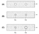
まず、基板(固相)10の表面に、図1(A)に示されるように、レジスト膜12を形成し、第1の凹部を形成する領域に開口を設ける。このときの平面図を図2(A)に示す。図示されるように、本実施形態において開口は円形状である。基板10の材料は、エッチング法によって好適に加工可能なものであれば特に限定されないが、本実施形態ではシリコン基板であるものとする。
First, as shown in FIG. 1A, a
ここで、レジスト膜12は、例えばフォトリソグラフィー法により得ることができる。具体的には、基板10上にレジスト材料を塗布した後、上記開口の形状に対応したフォトマスクを介してこのレジスト材料をi線、紫外線、電子線等により露光・現像することによって形成することができる。レジスト材料は、ネガ型であってもポジ型であってもよく、ネガ型のレジスト材料としては、ロジン−重クロム酸塩、ポリビニルアルコール(PVA)−重クロム酸塩、セラック−重クロム酸塩、カゼイン−重クロム酸塩、PVA−ジアゾ、アクリル系フォトレジスト等のような水溶性フォトレジスト、ポリケイ皮酸ビニル、環化ゴム−アジド、ポリビニルシンナミリデンアセタート、ポリケイ皮酸β−ビニロキシエチルエステル等のような油溶性フォトレジスト等が挙げられ、ポジ型のレジスト材料としては、o−ナフトキノンジアジド等のような油溶性フォトレジスト等が挙げられる。
Here, the
レジスト材料は、無機溶媒、各種有機溶媒、またはこれらの混合溶媒を適宜選択し、これに溶解または分散させ、スピン塗布法、スキャン塗布法、スプレー塗布法、スキージ塗布法等、公知の方法基板10表面に塗布することができる。
As the resist material, an inorganic solvent, various organic solvents, or a mixed solvent thereof is appropriately selected and dissolved or dispersed therein, and a known
続いて、レジスト膜12をマスクとしてエッチング法により第1の凹部13aおよび13bを形成する。エッチング法は、精度の良い加工が可能なドライエッチングが好ましい。尚、本実施形態では、比較のため、第1の凹部13bにのみ第2の凹部を形成する。
Subsequently,
次に、図1(C)に示すようにレジスト膜12を基板10から除去する。本工程は任意であるが、一旦レジスト膜12を除去した後で、第2の凹部を形成するためのレジスト膜を新たに形成することにより、当該レジスト膜を均一な厚さに形成しやすい。
Next, the
レジスト膜12を除去した後、同図(D)に示されるように第1の凹部13aおよび13bの底部と内壁、ならびに基板10表面を覆うレジスト膜14を形成する。レジスト膜14は、上述したとおり、液状のレジスト材料をスピン塗布法、スキャン塗布法、スプレー塗布法、スキージ塗布法等、公知の方法によって基板10表面に塗布することによって形成することができる。中でもスプレー塗布法を用いれば、1回の塗布工程によって、基板10表面と第1の凹部の底部および内壁に均一な厚さのレジスト膜12を形成することができる。スピン塗布法、スキャン塗布法、スキージ塗布法等を用いる場合は、塗布工程後、図3に示すように凹部がレジスト膜14’で埋め尽くされる。このような場合は、第1の凹部の上部に、第1の凹部の直径よりも小さな径の開口を有するマスクを設けて光を照射し、現像することによって、レジスト膜14’を図1(D)に示されるように成形することができる。このようにレジスト膜14を均一な厚さとしておくことにより、後でレジスト膜14を剥離するのが容易となる。図1(D)に示される状態での概略平面図を図2(B)に示す。
After removing the
続いて、図1(E)に示すように、レジスト膜14に、適宜フォトマスクを介して露光、現像し、第1の凹部13bの開口部を含むより大きな開口を設ける。この時の概略平面図を図2(C)に示す。ここで設けられる開口を介して第2の凹部が設けられるため、当該開口の形状が第2の凹部の水平断面の形状となる。また、図1(E)に示されるように、第1の凹部13bの内壁に形成されたレジスト膜も、基板10表面から所定の深さまで除去する。レジスト膜14を除去する深さが、第2の凹部の深さとなる。レジスト膜14の除去は、所望の深さまでレジスト膜14が除去されるように、照射する光のエネルギー量を調節して行う。
Subsequently, as shown in FIG. 1E, the resist
次に図1(F)に示すように、レジスト膜14を介して基板10を加工し、第2の凹部15を形成する。第2の凹部15は、第1の凹部13bよりも、その水平断面の直径が大きく、深さは浅い。このような第2の凹部15を設けることによって、凹部の内部に段差構造を形成することができる。第2の凹部15の形成はレジスト膜14を介したエッチング法によって行うことができる。エッチング法としては、ドライエッチングが好ましく、シリコン基板10とレジスト膜14のエッチング速度の比(選択比)を大きく取れるICPドライエッチング装置を用いたエッチング法によって行うことが特に望ましい。
Next, as shown in FIG. 1F, the
ドライエッチング法は、チャンバと、チャンバ内にプラズマ発生用ガスを導入するための第1の導入バルブと、基板10を冷却する冷却媒体ガスを導入するための第2の導入バルブと、チャンバ内に対向するように設けられた一対の電極と、一方の電極側に設置された基板10を冷却媒体ガスが通過可能な連通孔を通じて冷却する冷却板と、基板10を固定するための設置台とを備えたドライエッチング装置を用いて行われる。まず、基板10を設置台に固定し、チャンバ内を減圧する。そして第2の導入バルブから導入した冷却媒体ガスを基板10の加工する側と反対側から吹き付けて冷却板および冷却媒体ガスの温度を伝えて冷却し、かつ、第1の導入バルブから導入したプラズマ発生用ガスを一対の電極間に供給した状態で、この電極間に高周波電圧を印加する。これにより、電極間の間でプラズマが発生し、生じたイオンや電子が形成されたレジスト膜14の開口部を介して基板10に衝突することにより、第2の凹部が形成される。
The dry etching method includes a chamber, a first introduction valve for introducing a plasma generating gas into the chamber, a second introduction valve for introducing a cooling medium gas for cooling the
プラズマ発生用ガスとしては、例えば、フッ素系ガス、塩素および臭素のうちの少なくとも1種を含有するハロゲン系ガス等が挙げられるが、本実施形態のように基板10がシリコン単結晶で構成される場合には、SF6、C4F8、CBrF3、CF4/O2、Cl2、SF6/N2/Ar、BCl2/Cl2/Arガスを用いるのが好ましく、特に、SF6およびC4F8ガスのうちのいずれかを単独で、またはこれらの混合ガスを用いるのが好ましく、これにより効率よく加工を行うことができる。
Examples of the plasma generating gas include a fluorine-based gas, a halogen-based gas containing at least one of chlorine and bromine, and the
冷却媒体ガスとしては、冷却効率に優れ、プラズマの発生に影響を与えないようなものであればよく、特に限定されるものではないが、例えば、ヘリウム、アルゴン、窒素などの不活性ガス等が挙げられ、これらの中でも、ヘリウムを主成分とするのが好ましい。ヘリウムは、特に冷却効果に優れるものであることから冷却媒体ガスとして好適に用いられる。 The cooling medium gas is not particularly limited as long as it is excellent in cooling efficiency and does not affect the generation of plasma, and examples thereof include inert gases such as helium, argon, and nitrogen. Among these, helium is preferred as the main component. Helium is preferably used as a cooling medium gas because it has a particularly excellent cooling effect.
また、冷却板の温度すなわち冷却媒体ガスの温度は、−20〜60℃程度であるのが好ましく、−10〜10℃程度であるのがより好ましい。これにより、基板10を冷却して適切な温度を維持することができるようになる。
Further, the temperature of the cooling plate, that is, the temperature of the cooling medium gas is preferably about −20 to 60 ° C., and more preferably about −10 to 10 ° C. Thereby, it becomes possible to cool the
最後に図1(G)に示すように、レジスト膜14を除去することにより、1段の段差を内部に有する凹部が得られる。レジスト膜14の剥離は、例えば大気圧または減圧下において酸素プラズマやオゾン蒸気に晒すこと、または、レジスト膜14を溶解し得るアセトン、アルキルベンゼンスルホン酸のようなレジスト剥離液に浸漬することにより、レジスト膜14を液状化して行うことができる。
Finally, as shown in FIG. 1G, by removing the resist
本発明に係る方法によれば、上述のように第1の凹部13aおよび13bの内部にもレジスト膜14を形成し、第2の凹部の形成のために必要な領域のみこのレジスト膜14を除去するので、ドライエッチング工程においても周囲はレジスト膜14によって保護される。従って、ドライエッチングを繰り返し行って多段構造を形成しても寸法精度を確保することが可能となる。
According to the method of the present invention, as described above, the resist
また、ドライエッチング法を用いると、一般に、プラズマにさらされたレジスト膜14が硬化して、凹部内のレジスト膜14の除去が困難になるという問題もある。しかしながら、本実施形態に係る方法によれば、上述のように、レジスト膜14を一様に薄く成形しておくため、レジスト膜14の除去が容易になる。
In addition, when the dry etching method is used, there is a problem that the resist
次に、図4に、図1(G)の後、再び本発明に係る凹部形成方法を行って第3の凹部を設け、凹部の内部に2段の段差を形成する方法の概略工程図を示す。まず、図4(B)に示すように、第1の凹部13a、13bおよび第2の凹部15の底部と内壁、並びに基板10の表面を覆うレジスト膜16を形成する。上述のように、レジスト膜16の塗布法によっては、第1の凹部13a、13bおよび第2の凹部15を埋め尽くすようにレジスト膜16が形成されるが、その場合は、適宜マスクを介して光を照射、現像して、レジスト膜16が一様な厚さとなるように成形しておく。
Next, FIG. 4 is a schematic process diagram of a method of forming the third recess by performing the recess forming method according to the present invention again after FIG. 1 (G), and forming two steps in the recess. Show. First, as shown in FIG. 4B, a resist
続いて、同図(C)に示すように、第2の凹部15の開口部を含む、より大きな開口をレジスト膜16に設けるとともに、第2の凹部15の内壁に形成されたレジスト膜16を、基板10表面から所定の深さまで除去する。当該開口の形状が、第3の凹部の水平断面の形状となり、当該深さが第3の凹部の深さとなる。
Subsequently, as shown in FIG. 3C, a larger opening including the opening of the
次に、同図(D)に示されるように、レジスト膜16を介してエッチング法により基板10を加工し、第3の凹部17を形成する。第3の凹部17は、第2の凹部15よりも直径が大きく深さが浅い円筒形である。
Next, as shown in FIG. 4D, the
最後に、レジスト膜16を除去すると、内部に2段の段差構造を形成されている凹部を得ることができる。
(電子機器)
次に、本発明に係る凹部形成方法によって凹部が設けられた基板を備える電子機器の一例として、インクジェット式プリンタのインクジェットヘッドを例に挙げて説明する。
Finally, when the resist
(Electronics)
Next, as an example of an electronic apparatus including a substrate having a recess provided by the recess forming method according to the present invention, an inkjet head of an inkjet printer will be described as an example.
本実施形態で製造されるインクジェットヘッド1は、図5に示されるインクジェット式プリンタ2のインクジェットヘッド1であり、図6及び図7に示されるように、ノズルプレート320と、流路形成基板100と、弾性膜50と弾性膜50上に設けられた圧電素子300と、リザーバ形成基板30と、リザーバ形成基板30上に設けられた圧電素子300と、リザーバ形成基板30と、リザーバ形成基板30上に設けられた駆動IC120とを備えている。このインクジェットヘッド1は、ピエゾジェット式ヘッドを構成する。
The ink jet head 1 manufactured in the present embodiment is the ink jet head 1 of the ink jet printer 2 shown in FIG. 5. As shown in FIGS. 6 and 7, the
このようなインクジェットヘッド1は、例えば、以下のようにして製造することができる。まず、流路形成基板100となるシリコン基板100’を熱酸化処理などをすることによって、二酸化シリコン膜からなる弾性膜50を形成し、続いて弾性膜50上に絶縁体膜55及び下電極膜60を形成する。次に、下電極膜60上に圧電素子300、リード電極90を形成した後、貫通孔110を完成する。そして、シリコン基板100’の圧電素子300が設けられている側の面とリザーバ形成基板30とを接着剤層35により接着する。この段階の断面図を図8(A)に示す。このように、この段階では、シリコン基板100’の一面側に、弾性膜50、絶縁体膜55、及びリザーバ形成基板30が設けられている。
Such an inkjet head 1 can be manufactured as follows, for example. First, an
この後、シリコン基板100’にインク室102と、インク供給路104、連通部103及び位置決め基準孔105により構成される凹部とを形成して流路形成基板100を得た後、流路形成基板100にノズルプレート320を貼り合わせる。そのため、流路形成基板100の凹部の内部には、ノズルプレート320を貼り合わせるための接着剤逃げのための段差構造を設ける必要があり、ここに、本発明に係る凹部形成方法が用いられる。
Thereafter, the
まず図8(B)に示されるように、シリコン基板100’のリザーバ形成基板30が貼り合わせられている側に、接着樹脂400を介して保護基板420を貼り合わせる。保護基板420は、加工によって部分的に強度が不足した場合にも、シリコン基板100’の加工を安定して継続するためのものである。
First, as shown in FIG. 8B, a
次に、図8(C)に示されるように、シリコン基板100’表面上に、レジスト膜422を設ける。レジスト膜422の材料、塗布方法は上述のとおりである。
Next, as shown in FIG. 8C, a resist
続いて、同図(D)に示されるように、ドライエッチング法を用いてシリコン基板100’にインク室102と位置決め基準孔105となる第1の凹部を形成する。ドライエッチング法は、基板100’の図中下側から冷却した不活性ガスを吹き付ける等の方法で冷却しながら行う。そして、レジスト膜422を上述の方法で除去することにより、同図(E)に示されるように、インク室102及び位置決め基準孔105が設けられた流路形成基板100が形成される。
Subsequently, as shown in FIG. 4D, a first recess that becomes the
次に、図9(A)に示されるように、第1の凹部であるインク室102、位置決め基準孔105の底部及び内壁、並びに流路形成基板100表面を覆うレジスト膜424を形成する。レジスト膜424は、上述したようにレジスト材料をスプレー塗布法により塗布して、図示されるように一様な厚さで形成する。スピン塗布法、スキャン塗布法、スキージ塗布法等で塗布し、インク室102及び位置決め基準孔105内を埋めるようにレジスト膜424が形成される場合は、フォトマスクを介して露光・現像することにより不要なレジスト膜を除去してインク室102及び位置決め基準孔105内のレジスト膜424も一様な厚さとしておくことが望ましい。
Next, as shown in FIG. 9A, a resist
次に、図9(B)に示されるように、レジスト膜424に、第1の凹部であるインク室102及び位置決め基準孔105の開口部を含む、より大きな開口を設ける。また、インク室102及び位置決め基準孔105の内壁に形成されたレジスト膜424も所定の深さまで除去する。レジスト膜424の除去は、上述したとおり、所定の形状のフォトマスクを介して露光、現像することによって行うことができ、インク室102及び位置決め基準孔105の内壁に形成されたレジスト膜424は、露光する際の光のエネルギーを調整することによって所望の深さまで除去することができる。
Next, as shown in FIG. 9B, a larger opening including the openings of the
続いて、図9(C)に示されるように、ドライエッチング法により、流路形成基板100を加工して、第2の凹部246を形成し、同図(D)に示されるように、残りのレジスト膜424、接着樹脂400、及び保護基板420を流路形成基板100から取り外す。こうして、インク室102として、その内壁に段差構造を有する凹部が形成される。
Subsequently, as shown in FIG. 9C, the flow
次に、流路形成基板100にノズルプレート320を貼り合わせてから駆動IC120を実装し、コンプライアンス基板40を接合する。さらに、駆動IC120と下電極膜60及びリード電極90の接続部60a、90aとの間をワイヤボンディングすることにより接続配線を形成し、インクジェットヘッド1が完成する。
Next, after the
このような構成とすることにより、流路形成基板100にノズルプレート320を貼り合わせる際、この第2の凹部246を接着剤逃げとして機能させることができる。
With this configuration, when the
以上、本発明に係る凹部形成方法を、インクジェットヘッドの製造方法を例に挙げて説明したが、本発明はこれらに限定されるものではなく、種々のマイクロデバイスの製造工程に用いることができる。また、本発明に係る凹部形成方法は、基板状の物質だけでなく、あらゆる固相表面に応用することが可能である。本発明に係る凹部形成方法を応用して製造される電子機器は、インクジェット式プリンタに限られない。また、本発明の凹部形成方法には、任意の目的の工程が1または2以上追加されていてもよい。 As described above, the method for forming a recess according to the present invention has been described by taking the method for manufacturing an inkjet head as an example. However, the present invention is not limited to these, and can be used in various microdevice manufacturing processes. Moreover, the recess forming method according to the present invention can be applied not only to a substrate-like substance but also to any solid phase surface. The electronic device manufactured by applying the recess forming method according to the present invention is not limited to an ink jet printer. In addition, in the method for forming a recess according to the present invention, one or two or more optional steps may be added.
10…基板、12、14、16、422、424…レジスト膜、13…第1の凹部、15…第2の凹部、17…第3の凹部、100…流路形成基板、102…インク室(第1の凹部)、105…位置決め基準孔(第1の凹部)、426…第2の凹部
DESCRIPTION OF
Claims (6)
固相表面に、第1の凹部を形成する第1工程と、
前記第1の凹部の底部及び内壁と、前記固相表面とを覆うレジスト膜を形成する第2工程と、
前記固相表面に形成された前記レジスト膜に、前記第1の凹部の開口部を含む、より大きな開口を設けると共に、前記第1の凹部の内壁に形成された前記レジスト膜を、前記固相表面から所定の深さまでを除去する第3工程と、
エッチング法により、前記第1の凹部より水平断面が大きく、前記レジスト膜を除去した深さと等しい深さを有する第2の凹部を形成し、残りのレジスト膜を除去する第4工程と、を含む凹部形成方法。 A method of forming a recess having an inner multi-stage structure,
A first step of forming a first recess in the solid phase surface;
A second step of forming a resist film covering the bottom and inner walls of the first recess and the solid phase surface;
The resist film formed on the solid phase surface is provided with a larger opening including the opening of the first recess, and the resist film formed on the inner wall of the first recess is formed on the solid phase. A third step of removing from the surface to a predetermined depth;
Forming a second recess having a horizontal section larger than the first recess and having a depth equal to the depth from which the resist film has been removed by etching, and removing the remaining resist film. Recess formation method.
An electronic device comprising a solid phase surface having a recess formed by the recess forming method according to claim 1.
Priority Applications (1)
| Application Number | Priority Date | Filing Date | Title |
|---|---|---|---|
| JP2005360858A JP2007165651A (en) | 2005-12-14 | 2005-12-14 | Recess formation method and electronic device |
Applications Claiming Priority (1)
| Application Number | Priority Date | Filing Date | Title |
|---|---|---|---|
| JP2005360858A JP2007165651A (en) | 2005-12-14 | 2005-12-14 | Recess formation method and electronic device |
Publications (1)
| Publication Number | Publication Date |
|---|---|
| JP2007165651A true JP2007165651A (en) | 2007-06-28 |
Family
ID=38248201
Family Applications (1)
| Application Number | Title | Priority Date | Filing Date |
|---|---|---|---|
| JP2005360858A Pending JP2007165651A (en) | 2005-12-14 | 2005-12-14 | Recess formation method and electronic device |
Country Status (1)
| Country | Link |
|---|---|
| JP (1) | JP2007165651A (en) |
Cited By (6)
| Publication number | Priority date | Publication date | Assignee | Title |
|---|---|---|---|---|
| EP2006158A2 (en) | 2007-06-22 | 2008-12-24 | Toyota Boshoku Kabushiki Kaisha | Member mounting structure |
| CN105383177A (en) * | 2014-08-29 | 2016-03-09 | 佳能株式会社 | method for manufacturing an element substrate |
| JP2016105442A (en) * | 2014-12-01 | 2016-06-09 | 株式会社ディスコ | Wafer processing method |
| JP2019072882A (en) * | 2017-10-13 | 2019-05-16 | キヤノン株式会社 | Method for working through substrate and method for manufacturing liquid discharge head |
| EP3536504A1 (en) * | 2018-03-05 | 2019-09-11 | Brother Kogyo Kabushiki Kaisha | Liquid discharge head and method of producing liquid discharge head |
| JP2020001342A (en) * | 2018-06-29 | 2020-01-09 | キヤノン株式会社 | Liquid ejection head and manufacturing method therefor |
-
2005
- 2005-12-14 JP JP2005360858A patent/JP2007165651A/en active Pending
Cited By (10)
| Publication number | Priority date | Publication date | Assignee | Title |
|---|---|---|---|---|
| EP2006158A2 (en) | 2007-06-22 | 2008-12-24 | Toyota Boshoku Kabushiki Kaisha | Member mounting structure |
| CN105383177A (en) * | 2014-08-29 | 2016-03-09 | 佳能株式会社 | method for manufacturing an element substrate |
| US9616666B2 (en) | 2014-08-29 | 2017-04-11 | Canon Kabushiki Kaisha | Method of manufacturing element substrate |
| JP2016105442A (en) * | 2014-12-01 | 2016-06-09 | 株式会社ディスコ | Wafer processing method |
| JP2019072882A (en) * | 2017-10-13 | 2019-05-16 | キヤノン株式会社 | Method for working through substrate and method for manufacturing liquid discharge head |
| EP3536504A1 (en) * | 2018-03-05 | 2019-09-11 | Brother Kogyo Kabushiki Kaisha | Liquid discharge head and method of producing liquid discharge head |
| US10870277B2 (en) | 2018-03-05 | 2020-12-22 | Brother Kogyo Kabushiki Kaisha | Liquid discharge head and method of producing liquid discharge head |
| US11325381B2 (en) | 2018-03-05 | 2022-05-10 | Brother Kogyo Kabushiki Kaisha | Liquid discharge head and method of producing liquid discharge head |
| JP2020001342A (en) * | 2018-06-29 | 2020-01-09 | キヤノン株式会社 | Liquid ejection head and manufacturing method therefor |
| JP7237480B2 (en) | 2018-06-29 | 2023-03-13 | キヤノン株式会社 | Liquid ejection head and manufacturing method thereof |
Similar Documents
| Publication | Publication Date | Title |
|---|---|---|
| WO2009119064A1 (en) | Method for processing a substrate, method for manufacturing a semiconductor chip, and method for manufacturing a semiconductor chip having a resin adhesive layer | |
| JP2007165651A (en) | Recess formation method and electronic device | |
| JPWO2009154173A1 (en) | Multi-stage substrate manufacturing method | |
| JP2006212476A (en) | Film pattern forming method, film pattern, resist film, insulated film, circuit board, semiconductor device, surface acoustic wave device, surface acoustic wave oscillation device, electro-optical device and electronic equipment | |
| KR20040100890A (en) | Manufacturing method of thin film apparatus, electro-optical device, and electronic instrument | |
| US20100216260A1 (en) | Plasma etching method and apparatus, and method of manufacturing liquid ejection head | |
| JP5203340B2 (en) | Manufacturing method of semiconductor device | |
| KR100562593B1 (en) | Manufacturing method of fine structure, optical element, integrated circuit, and electronic instrument | |
| JP2016221866A (en) | Production method of liquid discharge head | |
| JP2008143068A (en) | Pattern forming method and manufacturing process of droplet discharge head | |
| US11380648B2 (en) | Process for manufacturing assembly pads on a carrier for the self-assembly of an electronic circuit on the carrier | |
| JP2009226660A (en) | Method for patterning by dry etching, mold used for it and method for manufacturing inkjet head | |
| JP2007158231A (en) | Substrate processing method, protection substrate, and electronic apparatus | |
| US20060270220A1 (en) | Plasma processing apparatus and method | |
| JP2006204991A (en) | Method of forming film pattern, film pattern, resist film, insulation film, circuit board, semiconductor device, surface acoustic wave device, surface acoustic wave generator, electro-optical device and electronic equipment | |
| JP4944514B2 (en) | Printing plate manufacturing method | |
| US8808553B2 (en) | Process for producing a liquid ejection head | |
| JP2007144799A (en) | Method for processing substrate, and electronic apparatus | |
| JP2004103496A (en) | Film-forming method, film-forming device, optical element, organic electroluminescent element, semiconductor element, and electronic equipment | |
| KR20050067033A (en) | Manufacturing method of ink jet recording head and ink jet recording head manufactured by manufacturing method | |
| JP2003142475A (en) | Method for manufacturing semiconductor device | |
| JP2020010018A (en) | Semiconductor element, method of manufacturing semiconductor element, and liquid ejection head | |
| KR20230135511A (en) | Method of manufacturing chip | |
| CN117038580A (en) | Method for manufacturing chip | |
| JP2007144915A (en) | Process for manufacturing liquid drop ejection head and patterning method |