JP2007140435A - Thin film transistor array, transflective thin film transistor liquid crystal display, lcd device, and electronic device - Google Patents
Thin film transistor array, transflective thin film transistor liquid crystal display, lcd device, and electronic device Download PDFInfo
- Publication number
- JP2007140435A JP2007140435A JP2006028110A JP2006028110A JP2007140435A JP 2007140435 A JP2007140435 A JP 2007140435A JP 2006028110 A JP2006028110 A JP 2006028110A JP 2006028110 A JP2006028110 A JP 2006028110A JP 2007140435 A JP2007140435 A JP 2007140435A
- Authority
- JP
- Japan
- Prior art keywords
- substrate
- thin film
- film transistor
- region
- display panel
- Prior art date
- Legal status (The legal status is an assumption and is not a legal conclusion. Google has not performed a legal analysis and makes no representation as to the accuracy of the status listed.)
- Pending
Links
- 239000010409 thin film Substances 0.000 title claims abstract description 62
- 239000004973 liquid crystal related substance Substances 0.000 title claims description 23
- 239000000758 substrate Substances 0.000 claims abstract description 88
- 230000005540 biological transmission Effects 0.000 claims description 19
- 239000010408 film Substances 0.000 claims description 6
- 238000010586 diagram Methods 0.000 description 4
- 238000012986 modification Methods 0.000 description 3
- 230000004048 modification Effects 0.000 description 3
- 238000000034 method Methods 0.000 description 2
- 230000003466 anti-cipated effect Effects 0.000 description 1
- 238000004519 manufacturing process Methods 0.000 description 1
- 239000012528 membrane Substances 0.000 description 1
- 230000005693 optoelectronics Effects 0.000 description 1
- 230000005855 radiation Effects 0.000 description 1
- 239000004065 semiconductor Substances 0.000 description 1
- 230000007704 transition Effects 0.000 description 1
Images


Classifications
-
- G—PHYSICS
- G02—OPTICS
- G02F—OPTICAL DEVICES OR ARRANGEMENTS FOR THE CONTROL OF LIGHT BY MODIFICATION OF THE OPTICAL PROPERTIES OF THE MEDIA OF THE ELEMENTS INVOLVED THEREIN; NON-LINEAR OPTICS; FREQUENCY-CHANGING OF LIGHT; OPTICAL LOGIC ELEMENTS; OPTICAL ANALOGUE/DIGITAL CONVERTERS
- G02F1/00—Devices or arrangements for the control of the intensity, colour, phase, polarisation or direction of light arriving from an independent light source, e.g. switching, gating or modulating; Non-linear optics
- G02F1/01—Devices or arrangements for the control of the intensity, colour, phase, polarisation or direction of light arriving from an independent light source, e.g. switching, gating or modulating; Non-linear optics for the control of the intensity, phase, polarisation or colour
- G02F1/13—Devices or arrangements for the control of the intensity, colour, phase, polarisation or direction of light arriving from an independent light source, e.g. switching, gating or modulating; Non-linear optics for the control of the intensity, phase, polarisation or colour based on liquid crystals, e.g. single liquid crystal display cells
- G02F1/133—Constructional arrangements; Operation of liquid crystal cells; Circuit arrangements
- G02F1/1333—Constructional arrangements; Manufacturing methods
- G02F1/1335—Structural association of cells with optical devices, e.g. polarisers or reflectors
- G02F1/133553—Reflecting elements
- G02F1/133555—Transflectors
-
- G—PHYSICS
- G02—OPTICS
- G02F—OPTICAL DEVICES OR ARRANGEMENTS FOR THE CONTROL OF LIGHT BY MODIFICATION OF THE OPTICAL PROPERTIES OF THE MEDIA OF THE ELEMENTS INVOLVED THEREIN; NON-LINEAR OPTICS; FREQUENCY-CHANGING OF LIGHT; OPTICAL LOGIC ELEMENTS; OPTICAL ANALOGUE/DIGITAL CONVERTERS
- G02F1/00—Devices or arrangements for the control of the intensity, colour, phase, polarisation or direction of light arriving from an independent light source, e.g. switching, gating or modulating; Non-linear optics
- G02F1/01—Devices or arrangements for the control of the intensity, colour, phase, polarisation or direction of light arriving from an independent light source, e.g. switching, gating or modulating; Non-linear optics for the control of the intensity, phase, polarisation or colour
- G02F1/13—Devices or arrangements for the control of the intensity, colour, phase, polarisation or direction of light arriving from an independent light source, e.g. switching, gating or modulating; Non-linear optics for the control of the intensity, phase, polarisation or colour based on liquid crystals, e.g. single liquid crystal display cells
- G02F1/133—Constructional arrangements; Operation of liquid crystal cells; Circuit arrangements
- G02F1/1333—Constructional arrangements; Manufacturing methods
- G02F1/1343—Electrodes
- G02F1/134309—Electrodes characterised by their geometrical arrangement
-
- G—PHYSICS
- G02—OPTICS
- G02F—OPTICAL DEVICES OR ARRANGEMENTS FOR THE CONTROL OF LIGHT BY MODIFICATION OF THE OPTICAL PROPERTIES OF THE MEDIA OF THE ELEMENTS INVOLVED THEREIN; NON-LINEAR OPTICS; FREQUENCY-CHANGING OF LIGHT; OPTICAL LOGIC ELEMENTS; OPTICAL ANALOGUE/DIGITAL CONVERTERS
- G02F2201/00—Constructional arrangements not provided for in groups G02F1/00 - G02F7/00
- G02F2201/12—Constructional arrangements not provided for in groups G02F1/00 - G02F7/00 electrode
- G02F2201/122—Constructional arrangements not provided for in groups G02F1/00 - G02F7/00 electrode having a particular pattern
Abstract
Description
本発明は、薄膜トランジスタアレイ(TFTアレイ)に関するものである。特に高開口率を有する半透過型(トランスフレクィブ)薄膜トランジスタ液晶ディスプレイ(TFT-LCD)に関するものである。 The present invention relates to a thin film transistor array (TFT array). In particular, the present invention relates to a transflective thin film transistor liquid crystal display (TFT-LCD) having a high aperture ratio.
現代人のライフスタイルに合わせるため、ビデオや映像機器がより軽く且つスリムになっている。従来のブラウン管(CRT)は多くの利点を持っているが、電子銃についての設計がCRTを重くかつ大きくさせる。また、少量の放射線の生成により視聴者の目を傷つける危険が常に存在する。半導体デバイス及びオプトエレクトロニックデバイスの製造技術の躍進につれて、フラットパネル・ディスプレイ例えば液晶ディスプレイ(LCD)、有機発光ディスプレイ(OLED)とプラズマディスプレイパネル(PDP)が次第にディスプレイ製品の主流になってきている。 Video and video equipment are becoming lighter and slimmer to fit the modern lifestyle. While conventional cathode ray tubes (CRTs) have many advantages, the design for the electron gun makes the CRT heavier and larger. In addition, there is always a danger of damaging the viewer's eyes due to the generation of small amounts of radiation. As the manufacturing technology of semiconductor devices and optoelectronic devices progresses, flat panel displays such as liquid crystal displays (LCDs), organic light emitting displays (OLEDs) and plasma display panels (PDPs) are gradually becoming mainstream display products.
光源によって、液晶ディスプレイは三種類に分類される。すなわち反射型LCD、透過型LCDと半透過型LCDである。半透過型LCDを例として挙げると、半透過型LCDは主に液晶パネルとバックライトモジュールとを備える。半透過型LCDパネルは二枚の透明な基板とその間に挟持された液晶層とを備える。バックライトモジュールは映像を表示するために表面光源を提供し液晶パネルを照射する。さらに具体的に言うと、半透過型LCDパネルは複数のピクセルを有し、各ピクセルは透過リージョンと反射リージョンとをそれぞれ備える。前記透過リージョンと反射リージョンとは異なるセルギャップを有する。 Liquid crystal displays are classified into three types according to the light source. That is, a reflective LCD, a transmissive LCD, and a transflective LCD. Taking a transflective LCD as an example, the transflective LCD mainly includes a liquid crystal panel and a backlight module. The transflective LCD panel includes two transparent substrates and a liquid crystal layer sandwiched between them. The backlight module provides a surface light source to display an image and illuminates the liquid crystal panel. More specifically, the transflective LCD panel has a plurality of pixels, and each pixel includes a transmissive region and a reflective region. The transmissive region and the reflective region have different cell gaps.
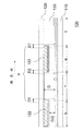
図1は従来の半透過型LCDパネルを模式的に示す上面図であり、図2は図1に示されている従来の半透過型LCDパネルのA-Aラインに沿った模式的断面図である。図1と図2を参照すると、従来の半透過型LCDパネル100は薄膜トランジスタアレイ110と、カラーフィルター120と、液晶層130とを備える。カラーフィルター120は薄膜トランジスタアレイ110の上側に配置され、液晶層130は薄膜トランジスタアレイ110とカラーフィルター120の間に狭持されている。
FIG. 1 is a top view schematically showing a conventional transflective LCD panel, and FIG. 2 is a schematic cross-sectional view taken along the line AA of the conventional transflective LCD panel shown in FIG. Referring to FIGS. 1 and 2, a conventional
図1と図2を参照すると、従来の薄膜トランジスタアレイ110においては、複数の半透過型ピクセルPがその上に形成されている。各半透過型ピクセルPは透過リージョンTと反射リージョンRとを有する。突起層122がカラーフィルター120の表面に形成されたため、半透過型ピクセルPの反射リージョンRとカラーフィルター120との間にセルギャップG/2が形成されているが、半透過型ピクセルPの透過リージョンTとカラーフィルター120との間にセルギャップGが形成されている。
Referring to FIGS. 1 and 2, in the conventional thin
図1と図2に示されているように、薄膜トランジスタアレイ110の同じ列において、多数のピクセルPの反射リージョンRと透過リージョンTが交互に設置されているため、逆傾斜領域D1、D2はピクセルP内のエリアに形成されているだけではなく、各ピクセルPの端部においても形成されている。さらに詳しく言うと、厚さ過渡エリアが突起層122の端部に形成されたため、逆傾斜領域(リバース・ティルト・ドメイン)D1、D2は各ピクセルPの端部とピクセルP内において薄膜トランジスタアレイ110の透過リージョンTと反射リージョンRとの間のエリアに対応するエリアに形成されている。従って、従来の半透過型LCDパネル100の開口率が各ピクセルPの端部に形成された逆傾斜領域D1によって制限されている。高開口率を有する高解像度LCDパネルを得るため、逆傾斜領域(リバース・ティルト・ドメイン)は低減されなければならない。
As shown in FIGS. 1 and 2, since the reflective regions R and the transmissive regions T of many pixels P are alternately arranged in the same column of the thin
本発明は、隣りのピクセルの透過リージョンを隣接させるよう構成することにより、高開口率を有する半透過型薄膜トランジスタ液晶ディスプレイを提供する。本発明の一つの実施例において、隣りの透過リージョンが接している。 The present invention provides a transflective thin-film transistor liquid crystal display having a high aperture ratio by configuring adjacent transmissive regions of adjacent pixels. In one embodiment of the invention, adjacent transparent regions are in contact.
ここに具体化され且つ広く記述されたように、本発明は薄膜トランジスタアレイ基板を提供する。該薄膜トランジスタアレイ基板は、基板と、この基板に配置され且つ第一方向に沿って配列された第一ピクセルグループと第二ピクセルグループとを備える。前記第一ピクセルグループは、第一反射リージョンと第一透過リージョンとを有し、前記第二ピクセルグループは第二透過リージョンと第二反射リージョンとを有し、これらのリージョンは第二方向に沿って配列されている。前記第一方向は前記第二方向と直交し、且つ前記第一透過リージョンと前記第二透過リージョンとは接している。 As embodied and broadly described herein, the present invention provides a thin film transistor array substrate. The thin film transistor array substrate includes a substrate, and a first pixel group and a second pixel group arranged on the substrate and arranged in a first direction. The first pixel group has a first reflective region and a first transmissive region, and the second pixel group has a second transmissive region and a second reflective region, and these regions are along a second direction. Are arranged. The first direction is orthogonal to the second direction, and the first transmission region and the second transmission region are in contact with each other.
ここに具体化され且つ広く記述されたように、本発明は半透過型薄膜トランジスタ液晶ディスプレイを提供する。該液晶ディスプレイは上述した薄膜トランジスタアレイ基板と、前記薄膜トランジスタアレイ基板の上側に配置されたカラーフィルター基板と、前記カラーフィルター基板と前記薄膜トランジスタアレイ基板との間に設置された液晶層とを備える。 As embodied and broadly described herein, the present invention provides a transflective thin film transistor liquid crystal display. The liquid crystal display includes the above-described thin film transistor array substrate, a color filter substrate disposed above the thin film transistor array substrate, and a liquid crystal layer disposed between the color filter substrate and the thin film transistor array substrate.
ここに具体化され且つ広く記述されたように、本発明は上述した半透過型薄膜トランジスタ液晶ディスプレイを備える液晶ディスプレイデバイスを提供する。 As embodied and broadly described herein, the present invention provides a liquid crystal display device comprising the transflective thin film transistor liquid crystal display described above.
ここに具体化され且つ広く記述されたように、本発明は上述した半透過型薄膜トランジスタ液晶ディスプレイを備える電子デバイスを提供する。 As embodied and broadly described herein, the present invention provides an electronic device comprising the transflective thin film transistor liquid crystal display described above.
本発明の一つ、一部分または全部、及び他の特徴と利点は当業者によれば、下記の説明により即座に明らかになる。本発明を実施するのに最も適切な一つの形態を簡単に例示することによって、本発明の好適な実施形態を示し説明する。認識されるように、本発明は異なる実施形態が可能であり、且つ本発明の要旨を逸脱しない範囲でいくつかの細部は多様且つ自明な態様に変更できる。従って、図面及び説明は制限ではなく事実上の例示であると見なされるべきである。 One, part or all of the present invention and other features and advantages will be readily apparent to those skilled in the art from the following description. A preferred embodiment of the invention will be shown and described by a simple illustration of one of the most suitable forms for carrying out the invention. It will be appreciated that the invention is capable of different embodiments and that several details are capable of modifications in various and obvious aspects, without departing from the spirit of the invention. Accordingly, the drawings and description are to be regarded as illustrative in nature and not as restrictive.
添付した図面は本発明のさらなる理解を得るために用いられ、本明細書に組み入れられ且つ明細書の一部分を構成する。図面は本発明の実施例を図解し、記述とともに本発明の原理を説明する役割を果たす。 The accompanying drawings are used to provide a further understanding of the invention and are incorporated in and constitute a part of this specification. The drawings illustrate embodiments of the invention and, together with the description, serve to explain the principles of the invention.
図3は本発明の一つの実施例による半透過型LCDパネルを模式的に示す上面図であり、図4は図3に示されている本発明の一つの実施例による半透過型LCDパネルのB-Bラインに沿った模式的断面図である。図3と図4を参照すると、本発明の半透過型LCDパネル200は薄膜トランジスタアレイ基板210と、カラーフィルター基板220と、液晶層230とを備える。カラーフィルター基板220は薄膜トランジスタアレイ基板210の上側に配置され、液晶層230は薄膜トランジスタアレイ基板210とカラーフィルター基板220の間に狭持されている。
FIG. 3 is a top view schematically showing a transflective LCD panel according to one embodiment of the present invention, and FIG. 4 is a plan view of the transflective LCD panel according to one embodiment of the present invention shown in FIG. It is a typical sectional view along a BB line. 3 and 4, the
図3と図4を参照すると、本発明のこの例示された実施例において、薄膜トランジスタアレイ基板210は基板212と、基板212に配置された複数の走査線214と、基板212に配置された複数のデータ線216と、基板212に配置された第一ピクセルグループ218aと、基板212に配置された第二ピクセルグループ218bとを備える。走査線214、データ線216、第一ピクセルグループ218a及び第二ピクセルグループ218bの配置は当業者にとって周知であり、従って本発明を理解するための更なる説明は不必要である。第一ピクセルグループ218aは第一反射リージョンR1と第一透過リージョンT1とを有する。第二ピクセルグループ218bは第二透過リージョンT2と第二反射リージョンR2とを有する。第一ピクセルグループ218aと第二ピクセルグループ218bは走査線214とデータ線216により制御され且つ列方向に沿って交互に配列されている。図3と図4に示されているように、薄膜トランジスタアレイ基板210において、第一反射リージョンR1、第一透過リージョンT1、第二透過リージョンT2、及び第二反射リージョンR2が順に列方向に沿って配列されている。
3 and 4, in this illustrated embodiment of the present invention, the thin film
図3と図4に示されているように、第一ピクセルグループ218aは行方向に沿って配列された複数の第一ピクセルP1を有する。各第一ピクセルP1は第一薄膜トランジスタ219aと、第一反射電極219bと、第一透過電極219cとを備える。第一薄膜トランジスタ219aは走査線214の一つとデータ線216の一つとに電気的接続され、第一反射電極219bは第一薄膜トランジスタ219aに電気的接続され、第一透過電極219cは第一反射電極219bに電気的接続されており、第一反射電極219bと第一透過電極219cは列方向に沿って配列されている。
As shown in FIGS. 3 and 4, the
図3と図4に示されているように、第二ピクセルグループ218bは行方向に沿って配列された複数の第二ピクセルP2を有する。各第二ピクセルP2は第二薄膜トランジスタ219dと、第二透過電極219eと、第二反射電極219fとを備える。第二薄膜トランジスタ219dは走査線214の一つとデータ線216の一つとに電気的接続され、第二透過電極219eは第二薄膜トランジスタ219dに電気的接続され、第二反射電極219fは第二透過電極219eに電気的接続されており、第二透過電極219eと第二反射電極219fは列方向に沿って配列されている。
As shown in FIGS. 3 and 4, the
図3と図4に示されているように、カラーフィルター基板220は第二基板222と、第二基板222に配置された複数のカラーフィルター膜223と、第二基板222に配置された突起層224と、第二基板222を覆うように配置されたコモン電極226とを備える。複数の突起を有する突起層224は第一反射リージョンR1と第二反射リージョンR2の上側に設置されている。各突起がカラーフィルター基板220と薄膜トランジスタアレイ基板210との間の間隔を狭くさせる。別の実施例によれば、第一反射リージョンR1と第二反射リージョンR2の上側にある間隔の厚さを第一透過リージョンT1と第二透過リージョンT2の上側にある間隔の厚さの半分に等しくすることが可能である。コモン電極226はカラーフィルター膜223と突起層224とをカバーする。
As shown in FIGS. 3 and 4, the
薄膜トランジスタアレイ基板210の同じ列において、第一ピクセルP1の第一透過リージョンT1と第二ピクセルP2の第二透過リージョンT2は接するように配置されているため、逆傾斜領域D2だけが第一ピクセルP1内と第二ピクセルP2内のエリアに形成される。従って、図1と図2と比べると、各第一ピクセルP1と第二ピクセルP2の端部において逆傾斜領域D1がなくされたため、半透過型LCDパネル200の開口率をさらに高くすることが可能である。
In the same column of the thin film
図5は本発明の一つの実施例による他の半透過型LCDパネルを模式的に示す上面図であり、図6は図5に示されている本発明の一つの実施例による他の半透過型LCDパネルのC-Cラインに沿った模式的断面図である。図5と図6を参照すると、本発明の半透過型LCDパネル300は薄膜トランジスタアレイ基板310と、カラーフィルター基板320と、液晶層330とを備える。カラーフィルター基板320は薄膜トランジスタアレイ基板310の上側に配置され、液晶層330は薄膜トランジスタアレイ基板310とカラーフィルター基板320の間に狭持されている。
FIG. 5 is a top view schematically showing another transflective LCD panel according to one embodiment of the present invention, and FIG. 6 is another transflective according to one embodiment of the present invention shown in FIG. It is typical sectional drawing along CC line of a type | mold LCD panel. Referring to FIGS. 5 and 6, the
図5と図6を参照すると、本発明において、薄膜トランジスタアレイ基板310は基板312と、基板312に配置された複数の走査線314と、基板312に配置された複数のデータ線316と、基板312に配置された第一ピクセルグループ318aと、基板312に配置された第二ピクセルグループ318bとを備える。第一ピクセルグループ318aは第一反射リージョンR1と第一透過リージョンT1とを有する。第二ピクセルグループ318bは第二透過リージョンT2と第二反射リージョンR2とを有する。走査線314、データ線316、第一ピクセルグループ318a及び第二ピクセルグループ318bの配置は当業者にとって周知であるため、詳しい説明は省略する。第一ピクセルグループ318aと第二ピクセルグループ318bは走査線314とデータ線316により制御され且つ行方向に沿って交互に配列されている。図5と図6に示されているように、薄膜トランジスタアレイ基板310において、第一反射リージョンR1、第一透過リージョンT1、第二透過リージョンT2、及び第二反射リージョンR2が順に行方向に沿って配列されている。
Referring to FIGS. 5 and 6, in the present invention, the thin film
図5と図6に示されているように、第一ピクセルグループ318aは列方向に沿って配列された複数の第三ピクセルP3を有し、該第三ピクセルP3は第三薄膜トランジスタ319aと、第三反射電極319bと、第三透過電極319cとを備える。第三薄膜トランジスタ319aは走査線314の一つとデータ線316の一つとに電気的接続され、第三反射電極319bは第三薄膜トランジスタ319aに電気的接続され、第三透過電極319cは第三反射電極319bに電気的接続されており、第三反射電極319bと第三透過電極319cは行方向に沿って配列されている。
As shown in FIGS. 5 and 6, the
図5と図6に示されているように、各第二ピクセルグループ318bは列方向に沿って配列された複数の第四ピクセルP4を有し、各第四ピクセルP4は第四薄膜トランジスタ319dと、第四透過電極319eと、第四反射電極319fとを備える。第四薄膜トランジスタ319dは走査線314の一つとデータ線316の一つとに電気的接続され、第四透過電極319eは第四薄膜トランジスタ319dに電気的接続され、第四反射電極319fは第四透過電極319eに電気的接続されており、第四透過電極319eと第四反射電極319fは行方向に沿って配列されている。
As shown in FIGS. 5 and 6, each
図5と図6に示されているように、カラーフィルター基板320は第二基板322と、第二基板322に配置された複数のカラーフィルター膜323と、第二基板322に配置された突起層324と、第二基板322を覆うように配置されたコモン電極326とを備える。突起層324は第一反射リージョンR1と第二反射リージョンR2の上側に設置されている。コモン電極326はカラーフィルター膜323と突起層324をカバーする。
5 and 6, the
薄膜トランジスタアレイ基板310の同じ行において、第三ピクセルP3の第一透過リージョンT1と第四ピクセルP4の第二透過リージョンT2が連続的に配置されているため、逆傾斜領域D2だけが第三ピクセルP3内と第四ピクセルP4内のエリアに形成される。従って、各第三ピクセルP3と第四ピクセルP4の端部において逆傾斜領域D1がなくされたため、半透過型LCDパネル300の開口率をさらに増大させることが可能である。
In the same row of the thin film
図7は本発明の一つの実施例によるLCDデバイス(例えば、ディスプレイモニター)の模式図である。図7を参照すると、半透過型LCDパネル200または300を有するLCDデバイス400が提供される。例えば、本発明のLCDデバイス400は上述した半透過型LCDパネル200または300と、バックライトユニット410と、フレーム420と、ベゼル430と、イメージコントローラ440とを備える。半透過型LCDパネル200または300とバックライトユニット410はフレーム420により支えられる。半透過型LCDパネル200または300、バックライトユニット410とフレーム420はベゼル430により固定される。また、イメージコントローラ440は適切な方法により半透過型LCDパネル200または300とバックライトユニット410とに電気的に接続される。
FIG. 7 is a schematic diagram of an LCD device (eg, a display monitor) according to one embodiment of the present invention. Referring to FIG. 7, an
図8は本発明の一つの実施例による電子デバイス(例えば、ノートブックコンピューター、パーソナル・デジタル・アシスタント、デジタルカメラなど)の模式図である。図8を参照すると、半透過型LCDパネル200または300を有する電子デバイス500が提供されている。例えば、本発明の電子デバイス500は上述した半透過型LCDパネル200または300と、バックライトユニット510と、フレーム520と、ベゼル530と、イメージコントローラ540と、個々の電子デバイスのためのコントロール機能を実施するシステムコントローラ550とを備える。このシステムコントローラは例えばデータソース、データインターフェースなどの要素を含むことが可能である。半透過型LCDパネル200または300とバックライトユニット510はフレーム520により支えられる。半透過型LCDパネル200または300、バックライトユニット510とフレーム520はベゼル530により固定される。また、イメージコントローラ540及びシステムコントローラ550は適切な方法により半透過型LCDパネル200または300及びバックライトユニット510と直接または間接に電気的に接続される。
FIG. 8 is a schematic diagram of an electronic device (eg, notebook computer, personal digital assistant, digital camera, etc.) according to one embodiment of the present invention. Referring to FIG. 8, an
前述の本発明の好適な実施形態に関する記述は例示と説明のために示されている。開示された形態それ自体または典型的な実施形態は本発明を全て網羅しているものではないし、これらの形態に本発明を限定することを意図したものではない。従って、前述の説明は制限というよりむしろ例示的なものであるとみなされるべきである。もちろん、多数の変形と変更が当業者にとって明らかである。本発明の原理と最良の実用形態を最もよく説明するため、前記実施形態が選ばれ且つ記述された。その結果、当業者は、本発明の多様な実施形態およびその変更が特定の使用や予期される実施に好適であることが理解できる。特に示唆がない限り、本発明の範囲は添付された請求項と、そのすべての用語を最も広い意味で解釈した均等物とにより定められることを目的とする。当然な事であるが、当業者は、例示された実施形態において本発明の請求項に定義された本発明の要旨を逸脱しない範囲で変更することが可能である。また、要素や構成部分が本発明の請求項に明示的に列挙されるか否かにかかわらず、本発明の開示における要素および構成部分を公衆に寄贈することを目的としているものではない。 The foregoing description of the preferred embodiment of the present invention has been presented for purposes of illustration and description. The disclosed forms per se or typical embodiments are not intended to be exhaustive or to limit the invention to these forms. Accordingly, the foregoing description should be considered exemplary rather than limiting. Of course, many variations and modifications will be apparent to practitioners skilled in this art. The foregoing embodiments have been chosen and described in order to best explain the principles and the best practical forms of the invention. As a result, those skilled in the art will appreciate that the various embodiments of the present invention and modifications thereof are suitable for particular uses and anticipated implementations. Unless otherwise indicated, the scope of the present invention is intended to be defined by the appended claims and the equivalents of which all terms are interpreted in the broadest sense. Of course, those skilled in the art can make changes in the illustrated embodiments without departing from the spirit of the invention as defined in the claims of the invention. Moreover, it is not intended to donate the elements and components in the present disclosure to the public, regardless of whether the elements and components are explicitly listed in the claims of the present invention.
200 半透過型LCDパネル
210 薄膜トランジスタアレイ基板
212 基板
214 走査線
216 データ線
218a 第一ピクセルグループ
218b 第二ピクセルグループ
219a 第一薄膜トランジスタ
219b 第一反射電極
219c 第一透過電極
219d 第二薄膜トランジスタ
219e 第二透過電極
219f 第二反射電極
220 カラーフィルター基板
222 第二基板
223 カラーフィルター膜
224 突起層
226 コモン電極
230 液晶層
400 LCDデバイス
440 イメージコントローラ
500 電子デバイス
550 システムコントローラ
P1 第一ピクセル
P2 第二ピクセル
R1 第一反射リージョン
R2 第二反射リージョン
T1 第一透過リージョン
T2 第二透過リージョン
200 Transflective LCD panel
210 Thin film transistor array substrate
212 substrate
214 scan lines
216 data lines
218a 1st pixel group
218b Second pixel group
219a first thin film transistor
219b First reflective electrode
219c First transmissive electrode
219d second thin film transistor
219e Second transmissive electrode
219f Second reflective electrode
220 color filter substrate
222 Second board
223 Color filter membrane
224 Projection layer
226 Common electrode
230 Liquid crystal layer
400 LCD device
440 image controller
500 electronic devices
550 system controller
P1 first pixel
P2 second pixel
R1 first reflection region
R2 second reflection region
T1 first transparent region
T2 second transparent region
Claims (13)
前記基板に配置された第一ピクセルグループと、
前記基板に配置された第二ピクセルグループとを備え、
前記第一ピクセルグループは第一方向に沿って配列された複数の第一ピクセルを有し、前記第一ピクセルは第二方向に沿って配列された第一反射リージョンと第一透過リージョンとを備え、前記第一方向は前記第二方向と直交し、
前記第二ピクセルグループは前記第一方向に沿って配列された複数の第二ピクセルを有し、前記第二ピクセルは前記第二方向に沿って配列された第二透過リージョンと第二反射リージョンとを備え、前記第一透過リージョンは前記第二透過リージョンに接することを特徴とする薄膜トランジスタアレイ基板。 A substrate,
A first pixel group disposed on the substrate;
A second pixel group disposed on the substrate,
The first pixel group includes a plurality of first pixels arranged along a first direction, and the first pixel includes a first reflection region and a first transmission region arranged along a second direction. The first direction is orthogonal to the second direction;
The second pixel group includes a plurality of second pixels arranged along the first direction, and the second pixel includes a second transmission region and a second reflection region arranged along the second direction. The thin film transistor array substrate, wherein the first transmission region is in contact with the second transmission region.
前記第一反射リージョンは第一反射電極により画定され且つ前記第一透過リージョンは第一透過電極により画定され、
前記第二反射リージョンは第二反射電極により画定され且つ前記第二透過リージョンは第二透過電極により画定されることを特徴とする薄膜トランジスタアレイ基板。 The thin film transistor array substrate according to claim 1,
The first reflective region is defined by a first reflective electrode and the first transmissive region is defined by a first transmissive electrode;
The thin film transistor array substrate, wherein the second reflective region is defined by a second reflective electrode and the second transmissive region is defined by a second transmissive electrode.
各第一ピクセルは、前記基板に配置された走査線と、前記基板に配置されたデータ線と、前記走査線と前記データ線とに電気的接続されている薄膜トランジスタとを更に備えることを特徴とする薄膜トランジスタアレイ基板。 The thin film transistor array substrate according to claim 1,
Each first pixel further includes a scan line disposed on the substrate, a data line disposed on the substrate, and a thin film transistor electrically connected to the scan line and the data line. Thin film transistor array substrate.
各第二ピクセルは、前記基板に配置された走査線と、前記基板に配置されたデータ線と、前記走査線と前記データ線とに電気的接続されている薄膜トランジスタとを更に備えることを特徴とする薄膜トランジスタアレイ基板。 The thin film transistor array substrate according to claim 1,
Each second pixel further includes a scan line disposed on the substrate, a data line disposed on the substrate, and a thin film transistor electrically connected to the scan line and the data line. Thin film transistor array substrate.
前記薄膜トランジスタアレイ基板と関連して配置され、該薄膜トランジスタアレイ基板との間の間隔を画定するカラーフィルター基板と、
前記薄膜トランジスタアレイ基板と前記カラーフィルター基板との間に配設された液晶層とを備えることを特徴とする半透過型ディスプレイパネル。 A thin film transistor array substrate according to claim 1;
A color filter substrate disposed in association with the thin film transistor array substrate and defining a distance between the thin film transistor array substrate;
A transflective display panel comprising: a liquid crystal layer disposed between the thin film transistor array substrate and the color filter substrate.
前記カラーフィルター基板は前記第一透過リージョンと前記第二透過リージョンとのためのフィルター透過リージョンを画定することを特徴とする半透過型ディスプレイパネル。 The transflective display panel according to claim 5,
The transflective display panel, wherein the color filter substrate defines a filter transmission region for the first transmission region and the second transmission region.
前記フィルター透過リージョンは前記第一透過リージョンと第二透過リージョンとが接する領域を提供することを特徴とする半透過型ディスプレイパネル。 The transflective display panel according to claim 6,
The transflective display panel, wherein the filter transmissive region provides an area where the first transmissive region and the second transmissive region are in contact with each other.
カラーフィルター基板は第二基板と、前記第二基板に配置された複数のカラーフィルター膜と、前記第二基板に配置された突起層と、前記第二基板に配置されたコモン電極とを更に備え、
前記コモン電極は前記カラーフィルター膜と突起層とを覆うことを特徴とする半透過型ディスプレイパネル。 The transflective display panel according to claim 5,
The color filter substrate further includes a second substrate, a plurality of color filter films disposed on the second substrate, a protruding layer disposed on the second substrate, and a common electrode disposed on the second substrate. ,
The transflective display panel, wherein the common electrode covers the color filter film and the protrusion layer.
前記第一突起と前記第二突起は前記第一と第二反射リージョンにおけるカラーフィルター基板と薄膜トランジスタアレイ基板の間の間隔を狭くすることを特徴とする半透過型ディスプレイパネル。 The transflective display panel according to claim 8, wherein the protrusion layer has a first protrusion and a second protrusion.
The transflective display panel, wherein the first protrusion and the second protrusion narrow a distance between the color filter substrate and the thin film transistor array substrate in the first and second reflection regions.
前記第一突起と第二突起は、前記第一及び第二突起と前記第一及び第二反射リージョンとのそれぞれの間にある間隔を狭くすることを特徴とする半透過型ディスプレイパネル。 The transflective display panel according to claim 9,
The transflective display panel according to claim 1, wherein the first protrusion and the second protrusion narrow a distance between each of the first and second protrusions and the first and second reflection regions.
イメージコントローラとを備え、
前記イメージコントローラは前記半透過型ディスプレイパネルに接続され、前記半透過型ディスプレイパネルを制御してイメージを表示させることを特徴とするディスプレイデバイス。 A transflective display panel according to claim 5;
With an image controller,
The display device is connected to the transflective display panel, and controls the transflective display panel to display an image.
システムコントローラとを備え、
前記システムコントローラは前記ディスプレイデバイスのコントローラに接続されイメージを表示させることを特徴とする電子デバイス。 A display device according to claim 12;
With a system controller,
The system controller is connected to a controller of the display device and displays an image.
Applications Claiming Priority (1)
| Application Number | Priority Date | Filing Date | Title |
|---|---|---|---|
| US11/281,310 US20070109472A1 (en) | 2005-11-17 | 2005-11-17 | Thin film transistor array, transflective thin film transistor liquid crystal display, LCD device and electronic device |
Publications (1)
| Publication Number | Publication Date |
|---|---|
| JP2007140435A true JP2007140435A (en) | 2007-06-07 |
Family
ID=38040401
Family Applications (1)
| Application Number | Title | Priority Date | Filing Date |
|---|---|---|---|
| JP2006028110A Pending JP2007140435A (en) | 2005-11-17 | 2006-02-06 | Thin film transistor array, transflective thin film transistor liquid crystal display, lcd device, and electronic device |
Country Status (3)
| Country | Link |
|---|---|
| US (1) | US20070109472A1 (en) |
| JP (1) | JP2007140435A (en) |
| CN (1) | CN100431158C (en) |
Families Citing this family (5)
| Publication number | Priority date | Publication date | Assignee | Title |
|---|---|---|---|---|
| JP5151408B2 (en) * | 2007-11-08 | 2013-02-27 | Nltテクノロジー株式会社 | Transflective liquid crystal display device |
| CN102593131A (en) * | 2011-01-07 | 2012-07-18 | 京东方科技集团股份有限公司 | Semi-transmission and semi-reflection thin film transistor array substrate and method for manufacturing the same |
| CN103226270B (en) | 2013-05-03 | 2016-01-20 | 合肥京东方光电科技有限公司 | A kind of semitransparent semi-inverse liquid crystal display panel, display device and array base palte |
| KR102132883B1 (en) * | 2013-12-10 | 2020-07-13 | 삼성디스플레이 주식회사 | Organic light emitting display device and method of manufacturing thereof |
| KR20210052724A (en) * | 2019-10-30 | 2021-05-11 | 삼성디스플레이 주식회사 | Display panel and display apparatus including the same |
Citations (2)
| Publication number | Priority date | Publication date | Assignee | Title |
|---|---|---|---|---|
| JP2001042332A (en) * | 1999-08-03 | 2001-02-16 | Sharp Corp | Liquid crystal display device |
| JP2004341486A (en) * | 2003-04-21 | 2004-12-02 | Seiko Epson Corp | Liquid crystal display and electronic equipment |
Family Cites Families (15)
| Publication number | Priority date | Publication date | Assignee | Title |
|---|---|---|---|---|
| US5299039A (en) * | 1988-07-21 | 1994-03-29 | Proxima Corporation | Stacked display panel construction and method of aligning pixel elements thereof |
| US6624860B1 (en) * | 1998-01-26 | 2003-09-23 | Sharp Kabushiki Kaisha | Color filter layer providing transmitted light with improved brightness and display device using same |
| US6215538B1 (en) * | 1998-01-26 | 2001-04-10 | Sharp Kabushiki Kaisha | Liquid crystal display including both color filter and non-color filter regions for increasing brightness |
| US6697135B1 (en) * | 1999-10-27 | 2004-02-24 | Lg. Philips Lcd Co., Ltd. | Transflective liquid crystal display device having reflective and transmissive mode parity |
| KR100700635B1 (en) * | 2000-10-27 | 2007-03-27 | 엘지.필립스 엘시디 주식회사 | Color filter for using Transflective Liquid Crystal Display Device and Method for fabricating the same |
| US6690438B2 (en) * | 2001-04-06 | 2004-02-10 | Citizen Watch Co., Ltd. | Liquid crystal display panel |
| JP3898012B2 (en) * | 2001-09-06 | 2007-03-28 | シャープ株式会社 | Display device |
| SG102064A1 (en) * | 2001-12-25 | 2004-02-27 | Toray Industries | Color filter, liquid crystal display device, and method for making color filter |
| TW567377B (en) * | 2002-06-13 | 2003-12-21 | Toppoly Optoelectronics Corp | Transmission-reflection switch liquid crystal display |
| TW554444B (en) * | 2002-09-03 | 2003-09-21 | Toppoly Optoelectronics Corp | Manufacturing method for liquid crystal display |
| TW578128B (en) * | 2003-01-02 | 2004-03-01 | Toppoly Optoelectronics Corp | Display driving device and method |
| US6788367B2 (en) * | 2003-01-21 | 2004-09-07 | Toppoly Optoelectronics Corp. | Liquid crystal display device |
| CN100543522C (en) * | 2003-12-12 | 2009-09-23 | 鸿富锦精密工业(深圳)有限公司 | Fringe field switch type lcd device |
| TWI240107B (en) * | 2004-02-02 | 2005-09-21 | Toppoly Optoelectronics Corp | Transflective liquid crystal display |
| JP2005292709A (en) * | 2004-04-05 | 2005-10-20 | Toshiba Matsushita Display Technology Co Ltd | Liquid crystal display element |
-
2005
- 2005-11-17 US US11/281,310 patent/US20070109472A1/en not_active Abandoned
-
2006
- 2006-02-06 JP JP2006028110A patent/JP2007140435A/en active Pending
- 2006-04-07 CN CNB2006100727149A patent/CN100431158C/en not_active Expired - Fee Related
Patent Citations (2)
| Publication number | Priority date | Publication date | Assignee | Title |
|---|---|---|---|---|
| JP2001042332A (en) * | 1999-08-03 | 2001-02-16 | Sharp Corp | Liquid crystal display device |
| JP2004341486A (en) * | 2003-04-21 | 2004-12-02 | Seiko Epson Corp | Liquid crystal display and electronic equipment |
Also Published As
| Publication number | Publication date |
|---|---|
| US20070109472A1 (en) | 2007-05-17 |
| CN100431158C (en) | 2008-11-05 |
| CN1967849A (en) | 2007-05-23 |
Similar Documents
| Publication | Publication Date | Title |
|---|---|---|
| US9536905B2 (en) | Active matrix substrate and display device using same | |
| JP5024110B2 (en) | Electro-optical device and electronic apparatus | |
| US6914644B2 (en) | Liquid crystal device | |
| US9348182B2 (en) | Active matrix substrate and display device | |
| US8779430B2 (en) | Semiconductor device, active matrix substrate, and display device | |
| WO2012144174A1 (en) | Liquid crystal display device | |
| US9436043B2 (en) | Array substrate and liquid crystal display panel | |
| JP2006330609A (en) | Liquid crystal display device | |
| US20210272498A1 (en) | Display substrate, display panel and display device | |
| US10847109B2 (en) | Active matrix substrate and display panel | |
| JP2007140435A (en) | Thin film transistor array, transflective thin film transistor liquid crystal display, lcd device, and electronic device | |
| US20140110852A1 (en) | Active matrix substrate, and display device | |
| US10871691B2 (en) | Display device | |
| JP2015118190A (en) | Liquid crystal display device and electronic equipment | |
| US20080068522A1 (en) | Display device and a method of manufacturing the same | |
| JP2012155198A (en) | Electro-optic device and electronic apparatus | |
| JPH09243999A (en) | Liquid crystal display device | |
| JP2010230888A (en) | Electro-optical device and electronic apparatus | |
| WO2022056782A1 (en) | Display substrate, display panel and display device | |
| TWI534517B (en) | Liquid crystal display panel | |
| JP2006154120A (en) | Electrooptical device, and electronic appliance | |
| CN101592835A (en) | Dot structure, active assembly array base plate, display panel and display device | |
| US9766516B2 (en) | Display device | |
| CN110361901B (en) | Pixel array substrate and driving method thereof | |
| JP6326518B2 (en) | Liquid crystal display |
Legal Events
| Date | Code | Title | Description |
|---|---|---|---|
| A131 | Notification of reasons for refusal |
Free format text: JAPANESE INTERMEDIATE CODE: A131 Effective date: 20090707 |
|
| A02 | Decision of refusal |
Free format text: JAPANESE INTERMEDIATE CODE: A02 Effective date: 20100330 |