JP2007123747A - Optical transmitter - Google Patents
Optical transmitter Download PDFInfo
- Publication number
- JP2007123747A JP2007123747A JP2005317119A JP2005317119A JP2007123747A JP 2007123747 A JP2007123747 A JP 2007123747A JP 2005317119 A JP2005317119 A JP 2005317119A JP 2005317119 A JP2005317119 A JP 2005317119A JP 2007123747 A JP2007123747 A JP 2007123747A
- Authority
- JP
- Japan
- Prior art keywords
- bias
- modulator
- output
- optical transmitter
- control circuit
- Prior art date
- Legal status (The legal status is an assumption and is not a legal conclusion. Google has not performed a legal analysis and makes no representation as to the accuracy of the status listed.)
- Granted
Links
Images
Abstract
Description
この発明は、光伝送システムに用いられる光送信器の制御技術に関するものである。 The present invention relates to a control technique for an optical transmitter used in an optical transmission system.
従来の光伝送システム、特に波長多重光伝送システムに用いられる光送信器、及び光送信器を含む光送受信器においては、その伝送する距離に応じた変調方式を適用していた。
例えば、短距離向けには、半導体レーザダイオード(Laser Diode:以下LD)に対して、そのバイアス電流にデータ信号で変調をかけることにより、光出力のON/OFFを行う直接変調方式を適用し、長距離向けには、LDと外部変調器を組み合わせた外部変調方式を適用することが一般的であった。
In a conventional optical transmission system, in particular, an optical transmitter used in a wavelength division multiplexing optical transmission system, and an optical transceiver including the optical transmitter, a modulation method according to the transmission distance has been applied.
For example, for a short distance, a direct modulation method for turning ON / OFF the optical output by applying a data signal to the bias current is applied to a semiconductor laser diode (hereinafter referred to as LD). For long distances, it is common to apply an external modulation system that combines an LD and an external modulator.
特に、長距離向けの外部変調器としては、電界吸収型光変調器(EA:Electro Absorption、以降EA変調器と略す)をLDに集積化した変調器内蔵LDの他に、ニオブ酸リチウム(LiNbO3:以下、LN)結晶を用いたLN変調器が一般的に用いられている。LN変調器は、EA変調器と比較して波長依存性が小さいため、広範囲の波長範囲で使用するチューナブルLDと組合せる場合や、決まった波長で発光するLDと組み合わせて、DWDM(Dense Wavelength Division Multiplex)システムでの光送信器に用いられることが多い。 In particular, as an external modulator for a long distance, in addition to a modulator built-in LD in which an electroabsorption optical modulator (EA: Electro Absorption, hereinafter abbreviated as EA modulator) is integrated in the LD, lithium niobate (LiNbO) is used. 3 : LN modulator using LN crystal is generally used. Since the LN modulator is less wavelength-dependent than the EA modulator, it can be combined with a tunable LD that is used in a wide wavelength range, or in combination with an LD that emits light at a predetermined wavelength, thereby providing a DWDM (Dense Wavelength). Often used for optical transmitters in Division Multiplex systems.
LN変調器を用いた光送信器では、LDは自動パワー制御(Automatic Power Control:以下、APC)回路によって、LDへのバイアス電流を制御することによってLDの出力を一定に保つ。このLDからの出力光を受けたLN変調器は、内部のLN結晶にデータ変調信号による電圧を印加することで、光の屈折率を変化させ、位相を変化させる。そして、その相互干渉により、出力信号のON/OFFを行う。
また、温度変動や長時間バイアス印加によるDCバイアスドリフト(動作特性曲線のドリフト)の問題を解決するために、LN変調器の出力特性を一定に保つようにDCバイアスを印加するバイアス制御回路を有している(例えば、特許文献1参照)。動作特性曲線とは、出力光パワーが電圧の増加に対して周期的に増減するものとして表される。
In an optical transmitter using an LN modulator, the LD keeps the output of the LD constant by controlling the bias current to the LD by an automatic power control (hereinafter referred to as APC) circuit. The LN modulator that has received the output light from the LD changes the refractive index of the light and changes the phase by applying a voltage based on the data modulation signal to the internal LN crystal. The output signal is turned ON / OFF by the mutual interference.
In addition, in order to solve the problem of DC bias drift (drift of the operating characteristic curve) due to temperature fluctuations and long-time bias application, a bias control circuit that applies a DC bias to keep the output characteristics of the LN modulator constant is provided. (For example, refer to Patent Document 1). The operating characteristic curve is expressed as the output optical power periodically increasing / decreasing with increasing voltage.
しかしながら、電源投入時やデータ信号が無入力時に、LDがDisableされていて変調光のモニタができない場合、或いは故障発生時等の場合には、バイアス制御回路によるDCバイアス制御が不定となり、印加されるDCバイアスが最大値または最小値となる。
これらのバイアス点では、LDからの出力光(Continuous Wave:以下、CW光)に対して変調をかけることができず、無変調のままCW光を出力する恐れがある。
通常の変調光では光のON/OFFの割合が1:1となるため、平均電力はCW光の半分、即ち3dB下がった出力となる。しかし、無変調のCW光では光送信器に規定される送信電力より3dB上がったままで出力される恐れがあり、光送信器に接続される受光素子等の定格電力を超えてしまう場合があった。その結果、光伝送システム全体の信頼性低下を引き起こすという問題があった。
However, when the power is turned on or when no data signal is input, the LD is disabled and the modulated light cannot be monitored, or when a failure occurs, the DC bias control by the bias control circuit becomes indeterminate and applied. DC bias becomes the maximum value or the minimum value.
At these bias points, the output light from the LD (Continuous Wave: hereinafter referred to as CW light) cannot be modulated, and there is a possibility that the CW light is output without being modulated.
In the case of normal modulated light, the ON / OFF ratio of light is 1: 1, so the average power is an output that is half that of CW light, that is, 3 dB lower. However, unmodulated CW light may be output with 3 dB higher than the transmission power specified for the optical transmitter, and may exceed the rated power of the light receiving element connected to the optical transmitter. . As a result, there is a problem that the reliability of the entire optical transmission system is reduced.
従来の光送信器は、以上のように構成されていたので、電源投入時やデータ信号の無入力時、或いは装置故障時等に光送信器から過大に光出力が行われるという課題があった。 Since the conventional optical transmitter is configured as described above, there has been a problem that excessive optical output is performed from the optical transmitter when the power is turned on, when no data signal is input, or when the device is faulty. .
この発明は上記のような課題を解消するためになされたもので、光伝送システムにおいて、電源投入時等の過渡状態において、出力光の電力を規定値以下に押さえることが可能な光送信器を提供することを目的とする。 The present invention has been made to solve the above-described problems. In an optical transmission system, an optical transmitter capable of holding the power of output light below a specified value in a transient state such as when the power is turned on is provided. The purpose is to provide.
この発明に係る光送信器は、CW光を発出する半導体レーザダイオードと、前記半導体レーザダイオードの出力を一定に保つLD駆動回路と、前記半導体レーザダイオードからのCW光を変調するLN変調器と、入力されるデータ信号に応じて前記LN変調器へ駆動信号を出力する変調器駆動回路と、前記LN変調器でのDCバイアスドリフトを防止するバイアス制御回路と、光送信器が過渡状態の場合に、前記半導体レーザへのバイアス電流を通常の所定値より低く設定するように前記LD駆動回路の制御を行う出力制御回路とを備えている。 An optical transmitter according to the present invention includes a semiconductor laser diode that emits CW light, an LD drive circuit that maintains a constant output of the semiconductor laser diode, an LN modulator that modulates CW light from the semiconductor laser diode, A modulator driving circuit that outputs a driving signal to the LN modulator according to an input data signal, a bias control circuit that prevents a DC bias drift in the LN modulator, and an optical transmitter in a transient state And an output control circuit for controlling the LD drive circuit so as to set a bias current to the semiconductor laser lower than a normal predetermined value.
この発明によれば、光送信器が過渡状態の場合に、半導体レーザダイオードからの出力光を規定値以下に抑えることにより、光送信器に接続される受光素子の故障を防止することができる。その結果、信頼性の高い光伝送システムを提供することができる。 According to the present invention, when the optical transmitter is in a transient state, it is possible to prevent failure of the light receiving element connected to the optical transmitter by suppressing the output light from the semiconductor laser diode to a specified value or less. As a result, a highly reliable optical transmission system can be provided.
実施の形態1.
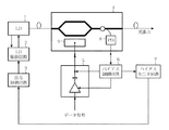
以下、この発明の実施の形態1について説明する。図1は、この発明の実施の形態1に係る光送信器の一例を示す構成図である。
図1において、本光送信器は、電源からのバイアス電流によりCW光を発出するLD 1、LD 1の出力パワーが一定値となるようにLD 1を制御するLD駆動回路2、LD 1の出力値を決定する出力制御回路3、LD 1からのCW光を変調するLN変調器4、LN変調器4に駆動信号を入力する変調器駆動回路5、LN変調器4のDCバイアスドリフトをキャンセル(防止)するバイアス制御回路6、バイアス制御回路6のバイアス制御値(DCバイアス信号)をモニタするバイアスモニタ回路7とを備えている。
また、LN変調器4は、変調後のCW光の出力値を検出するPD(Photo Detector)8と、変調器駆動回路5からの駆動信号が入力される信号電極9とを備えている。
Embodiment 1 FIG.
Embodiment 1 of the present invention will be described below. 1 is a block diagram showing an example of an optical transmitter according to Embodiment 1 of the present invention.
In FIG. 1, the present optical transmitter outputs LD 1 and LD 1 that control LD 1 so that the output power of LD 1 and LD 1 that emit CW light by a bias current from a power source becomes a constant value. The output control circuit 3 that determines the value, the LN modulator 4 that modulates the CW light from the LD 1, the modulator drive circuit 5 that inputs the drive signal to the LN modulator 4, and the DC bias drift of the LN modulator 4 are canceled ( A
The LN modulator 4 includes a PD (Photo Detector) 8 that detects an output value of the CW light after modulation, and a signal electrode 9 to which a drive signal from the modulator drive circuit 5 is input.
次に、動作について説明する。図1に示すように、出力制御回路3は、LD 1から一定出力のCW光が発出されるように、リファレンスとなる一定電圧(以下、リファレンス電圧)を、LD駆動回路2に供給する。
Next, the operation will be described. As shown in FIG. 1, the output control circuit 3 supplies a constant voltage serving as a reference (hereinafter referred to as a reference voltage) to the
LD駆動回路2では、LD 1からの光出力のモニタ電流を電流/電圧変換してモニタ電圧とした上で、このモニタ電圧とリファレンス電圧とを比較する。そして、比較結果に基づいて、LD 1からのCW光の出力を一定に保つように、APC制御でLD 1のバイアス電流を制御する。
In the
出力制御回路3をD/Aコンバータや電子可変抵抗等で構成することで、その出力を外部制御により変化させることができる。従って、モニタ電圧の状況に応じてリファレンス電圧を可変させることにより、LD 1からのCW光の出力を任意に可変させることが可能である。 By configuring the output control circuit 3 with a D / A converter, an electronic variable resistor, or the like, the output can be changed by external control. Therefore, it is possible to arbitrarily vary the output of the CW light from the LD 1 by varying the reference voltage according to the status of the monitor voltage.
変調器駆動回路5は、入力されたデータ信号を、LN変調器4を動作させるために必要な電界を有する電気信号(以下、データ変調信号)に変換する。そして、データ変調信号に対して、バイアス制御回路6によって生成されたDCバイアス信号を重畳することで、LN変調器4を駆動する駆動信号を生成する。
ここで、DCバイアス信号は、変調光を常に安定したものとするために、LN変調器4におけるDCバイアスドリフトを制御する信号である。
LN変調器4は、変調器駆動回路5からの駆動信号により、伝送に必要な変調光を得る。
The modulator driving circuit 5 converts the input data signal into an electric signal having an electric field necessary for operating the LN modulator 4 (hereinafter referred to as a data modulation signal). A drive signal for driving the LN modulator 4 is generated by superimposing the DC bias signal generated by the
Here, the DC bias signal is a signal for controlling the DC bias drift in the LN modulator 4 in order to always stabilize the modulated light.
The LN modulator 4 obtains modulated light necessary for transmission by the drive signal from the modulator drive circuit 5.
一方、バイアス制御回路6がDCバイアス信号を変調器駆動回路5に送出し、そのDCバイアス信号が重畳された駆動信号により、LN変調器4でLD1からのCW光を変調する際に、LN変調器4の内部で光カプラ等により変調光を一部分岐し、PD 8で電流変換して、バイアス制御回路6にフィードバックする。
バイアス制御回路6は、このフィードバックに基づいて、DCバイアスドリフトが生じないようにDCバイアス信号で変調器駆動回路5を制御する。
バイアスモニタ7は、バイアス制御回路6から変調器駆動回路5に送出されるDCバイアス信号、即ち、LN変調器4に印加されるDCバイアス(バイアス電圧)を常時モニタする。
On the other hand, when the
Based on this feedback, the
The bias monitor 7 constantly monitors a DC bias signal sent from the
ここで、電源投入時またはLD 1をEnableさせるリセット解除時等には、LD 1の出力制御回路3は、本来の光送信出力としてリファレンス電圧を設定するのではなく、一定時間その出力を所定値から下げて設定する。従って、上記過渡状態において、LN変調器4へのバイアス制御が不定になり、LN変調器4が入力されるCW光を変調できずにそのまま出力した場合であっても、CW光は規定値を上回るパワーとなることがない。
所定の時間が経過の後、出力制御回路3は、リファレンス電圧を段階的に本来の値に設定することで、LN変調器4でのDCバイアス制御の状態によらず、光送信器の出力値が過大となることがなくなる。
Here, when the power is turned on or when reset is performed to enable the LD 1, the output control circuit 3 of the LD 1 does not set the reference voltage as the original optical transmission output, but outputs the output for a predetermined time. Lower the setting. Therefore, even when the bias control to the LN modulator 4 becomes indefinite in the transient state and the CW light input by the LN modulator 4 is output without being modulated, the CW light has a specified value. The power will not exceed.
After the predetermined time has elapsed, the output control circuit 3 sets the reference voltage to the original value in a stepwise manner, so that the output value of the optical transmitter is independent of the state of the DC bias control in the LN modulator 4. No longer becomes excessive.
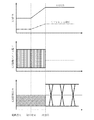
図2は、LD出力、LD出力を決定するリファレンス電圧、LN変調器におけるLN印加バイアス電圧、光送信器出力のそれぞれについて、電源投入時からの時間変化を模式的に示した図である。
図2において、電源投入時は、リファレンス電圧及びLD出力は所定値より低く設定される。しかし、LN変調器4におけるDCバイアス制御の状態により、変調時に光出力が3dB下がることなく出力される場合には、光送信器出力は規定値となる。
次に、LN変調器4のバイアスが正常に制御されることで、光送信器出力は変調の効果により3dB下がる(初期化完了)。3dB下がった後にリファレンス電圧を変化させ、所望の光送信器出力となる点に設定する(調整完了)。
従って、図2に示すように、光送信器出力が過大な状態がないことがわかる。
FIG. 2 is a diagram schematically showing temporal changes from when the power is turned on for the LD output, the reference voltage for determining the LD output, the LN applied bias voltage in the LN modulator, and the optical transmitter output.
In FIG. 2, when the power is turned on, the reference voltage and the LD output are set lower than predetermined values. However, when the optical output is output without being lowered by 3 dB during modulation due to the state of the DC bias control in the LN modulator 4, the output of the optical transmitter becomes a specified value.
Next, when the bias of the LN modulator 4 is normally controlled, the output of the optical transmitter is lowered by 3 dB due to the modulation effect (initialization is completed). After the voltage drops by 3 dB, the reference voltage is changed and set to a point where a desired optical transmitter output is obtained (adjustment completed).
Therefore, as shown in FIG. 2, it can be seen that there is no excessive state of the optical transmitter output.
また、LN変調器4のDCバイアスドリフトは、少なくとも数分単位で連続的にドリフトする。そのため、何らかの故障が原因でバイアス制御が不能となった場合、バイアス制御回路6から印加されるバイアス電圧の時間変化はそのバイアスドリフトによる時間変化よりも十分小さいものとなる。従って、バイアスモニタ7にて、時間的なバイアス電圧値の変化が通常モニタ時と比較して格段に大きくなった時点で、LDの出力制御回路3に対して、リファレンス電圧を運用中の状態から、所定値より低い前述の電源投入時の値に変化させることで、故障発生時にも光送信器からの光出力が過大となる状態を防止することができる。
Further, the DC bias drift of the LN modulator 4 continuously drifts in units of several minutes. Therefore, when the bias control becomes impossible due to some failure, the time change of the bias voltage applied from the
以上のように、この実施の形態1によれば、予め複数のLDバイアスを設定可能なバイアス制御回路6、LN変調器4におけるDCバイアスの急変をモニタするバイアスモニタ回路7、モニタ結果に基づいてLD駆動回路2にリファレンス電圧を供給する出力制御回路3を備えることにより、常に光送信器の出力光を所定の範囲内に制御することができ、光送信器に接続される光受信器の2次故障を防止することができる。その結果、信頼性の高い光伝送システムを提供することができる。
As described above, according to the first embodiment, the
1 LD(半導体レーザダイオード)、2 LD駆動回路、3 出力制御回路、4 LN変調器、5 変調器駆動回路、6 バイアス制御回路、7 バイアスモニタ回路、8 PD(Photo Detector)、9 信号電極。
1 LD (semiconductor laser diode), 2 LD drive circuit, 3 output control circuit, 4 LN modulator, 5 modulator drive circuit, 6 bias control circuit, 7 bias monitor circuit, 8 PD (Photo Detector), 9 signal electrode.
Claims (4)
前記半導体レーザダイオードの出力を一定に保つLD駆動回路と、
前記半導体レーザダイオードからのCW光を変調するLN変調器と、
入力されるデータ信号に応じて前記LN変調器へ駆動信号を出力する変調器駆動回路と、
前記LN変調器でのDCバイアスドリフトを防止するバイアス制御回路と、
光送信器が過渡状態の場合に、前記半導体レーザへのバイアス電流を通常の所定値より低く設定するように前記LD駆動回路の制御を行う出力制御回路とを備えた光送信器。 A semiconductor laser diode emitting CW light;
An LD driving circuit for keeping the output of the semiconductor laser diode constant;
An LN modulator for modulating CW light from the semiconductor laser diode;
A modulator driving circuit that outputs a driving signal to the LN modulator in response to an input data signal;
A bias control circuit for preventing DC bias drift in the LN modulator;
An optical transmitter comprising: an output control circuit that controls the LD driving circuit so that a bias current to the semiconductor laser is set lower than a normal predetermined value when the optical transmitter is in a transient state.
前記バイアス電圧のモニタ状態に応じて、前記出力制御回路が、前記半導体レーザダイオードへの前記バイアス電流を通常の所定値より低く設定する制御を行うことを特徴とする請求項1記載の光送信器。 A bias monitor circuit for monitoring a bias voltage applied to the LN modulator;
2. The optical transmitter according to claim 1, wherein the output control circuit performs control for setting the bias current to the semiconductor laser diode to be lower than a normal predetermined value in accordance with a monitoring state of the bias voltage. .
前記LD駆動回路は、前記リファレンス電圧に基づいて前記半導体レーザダイオードの出力を制御することを特徴とする請求項1または請求項2記載の光送信器。 The output control circuit outputs a reference voltage to the LD drive circuit,
3. The optical transmitter according to claim 1, wherein the LD driving circuit controls the output of the semiconductor laser diode based on the reference voltage.
前記変調器駆動回路は、入力されたデータ信号に前記バイアス制御回路からの前記DCバイアス信号を重畳して生成した前記駆動信号により、前記LN変調器でのDCバイアスドリフトを防止することを特徴とする請求項1から請求項3のうちのいずれか1項記載の光送信器。
The bias control circuit can set a plurality of DC bias signals in advance,
The modulator driving circuit prevents a DC bias drift in the LN modulator by the driving signal generated by superimposing the DC bias signal from the bias control circuit on an input data signal. The optical transmitter according to any one of claims 1 to 3.
Priority Applications (1)
| Application Number | Priority Date | Filing Date | Title |
|---|---|---|---|
| JP2005317119A JP4767657B2 (en) | 2005-10-31 | 2005-10-31 | Optical transmitter |
Applications Claiming Priority (1)
| Application Number | Priority Date | Filing Date | Title |
|---|---|---|---|
| JP2005317119A JP4767657B2 (en) | 2005-10-31 | 2005-10-31 | Optical transmitter |
Publications (2)
| Publication Number | Publication Date |
|---|---|
| JP2007123747A true JP2007123747A (en) | 2007-05-17 |
| JP4767657B2 JP4767657B2 (en) | 2011-09-07 |
Family
ID=38147228
Family Applications (1)
| Application Number | Title | Priority Date | Filing Date |
|---|---|---|---|
| JP2005317119A Expired - Fee Related JP4767657B2 (en) | 2005-10-31 | 2005-10-31 | Optical transmitter |
Country Status (1)
| Country | Link |
|---|---|
| JP (1) | JP4767657B2 (en) |
Cited By (3)
| Publication number | Priority date | Publication date | Assignee | Title |
|---|---|---|---|---|
| WO2009078435A1 (en) * | 2007-12-17 | 2009-06-25 | Fujikura Ltd. | Control device for external modulator and control method |
| JP2017515390A (en) * | 2014-04-23 | 2017-06-08 | マーポス、ソチエタ、ペル、アツィオーニMarposs S.P.A. | Apparatus and method for transmitting and receiving an alternating optical signal |
| WO2022110965A1 (en) * | 2020-11-24 | 2022-06-02 | 青岛海信宽带多媒体技术有限公司 | Optical module |
Citations (5)
| Publication number | Priority date | Publication date | Assignee | Title |
|---|---|---|---|---|
| JPH04192729A (en) * | 1990-11-27 | 1992-07-10 | Fujitsu Ltd | Optical transmitter |
| JP2000196185A (en) * | 1998-12-24 | 2000-07-14 | Fujitsu Ltd | Light transmitter |
| JP2001183613A (en) * | 1999-12-24 | 2001-07-06 | Sumitomo Osaka Cement Co Ltd | Light intensity modulating light source |
| JP2003229819A (en) * | 2002-02-04 | 2003-08-15 | Hitachi Cable Ltd | Optical transmitter |
| JP2005252806A (en) * | 2004-03-05 | 2005-09-15 | Furukawa Electric Co Ltd:The | Optical transmitter, optical transmission system and output control method |
-
2005
- 2005-10-31 JP JP2005317119A patent/JP4767657B2/en not_active Expired - Fee Related
Patent Citations (5)
| Publication number | Priority date | Publication date | Assignee | Title |
|---|---|---|---|---|
| JPH04192729A (en) * | 1990-11-27 | 1992-07-10 | Fujitsu Ltd | Optical transmitter |
| JP2000196185A (en) * | 1998-12-24 | 2000-07-14 | Fujitsu Ltd | Light transmitter |
| JP2001183613A (en) * | 1999-12-24 | 2001-07-06 | Sumitomo Osaka Cement Co Ltd | Light intensity modulating light source |
| JP2003229819A (en) * | 2002-02-04 | 2003-08-15 | Hitachi Cable Ltd | Optical transmitter |
| JP2005252806A (en) * | 2004-03-05 | 2005-09-15 | Furukawa Electric Co Ltd:The | Optical transmitter, optical transmission system and output control method |
Cited By (4)
| Publication number | Priority date | Publication date | Assignee | Title |
|---|---|---|---|---|
| WO2009078435A1 (en) * | 2007-12-17 | 2009-06-25 | Fujikura Ltd. | Control device for external modulator and control method |
| JPWO2009078435A1 (en) * | 2007-12-17 | 2011-04-28 | 株式会社フジクラ | External modulator control apparatus and control method |
| JP2017515390A (en) * | 2014-04-23 | 2017-06-08 | マーポス、ソチエタ、ペル、アツィオーニMarposs S.P.A. | Apparatus and method for transmitting and receiving an alternating optical signal |
| WO2022110965A1 (en) * | 2020-11-24 | 2022-06-02 | 青岛海信宽带多媒体技术有限公司 | Optical module |
Also Published As
| Publication number | Publication date |
|---|---|
| JP4767657B2 (en) | 2011-09-07 |
Similar Documents
| Publication | Publication Date | Title |
|---|---|---|
| JP4408010B2 (en) | Optical transmitter for WDM | |
| KR100909044B1 (en) | Light intensity and extinction ratio adjusting device and method | |
| US20090003843A1 (en) | Optical transmitter and method for control the same | |
| JPH11340919A (en) | Optical transmitter, terminal station device having the optical transmitter and optical communication system | |
| CA2619307C (en) | Optical transmitting apparatus and temperature controlling method used therefor | |
| US8036540B2 (en) | Optical transmitter suppressing wavelength deviation at beginning of operation | |
| US8036534B2 (en) | Optical transmitter outputting a plurality of signal light with a preset wavelength span | |
| US8116637B2 (en) | Optical transmitter with a chirp managed laser diode automatically adjusting emission wavelength thereof and its adjusting method | |
| JPH09191293A (en) | Optical transmitter | |
| JP4767657B2 (en) | Optical transmitter | |
| JP2019049695A (en) | Electron absorption bias circuit for an electron absorption modulator | |
| EP1484851A1 (en) | Faraday variable optical attenuator and optical transmitter including it | |
| US7031620B2 (en) | Optical transmission device and optical transmission system using the same | |
| EP1246327A2 (en) | Optical output control circuit for obtaining stable optical output power | |
| JP2001251254A (en) | Optical transmitter and optical transmission system | |
| US20030058507A1 (en) | Optical transmitter and wavelength division multiplexing transmission system | |
| JP5029276B2 (en) | Optical transmitter and temperature control method used therefor | |
| JP2762986B2 (en) | Optical output cutoff circuit | |
| JP2022171191A (en) | Optical sending device, optical transmission device, and optimum phase quantity calculation method | |
| JP2018014473A (en) | Method for controlling optical transceiver | |
| JP2010011098A (en) | Optical transmission device | |
| WO2018150584A1 (en) | Optical transmitter, temperature control device, and temperature control method | |
| JP2002368693A (en) | Optical transmitter | |
| JP2000089178A (en) | Method and device for light transmission | |
| KR100357625B1 (en) | Wavelength stabilization and automatic power control circuit of transponder in wavelength division multiplexing optical transmission system |
Legal Events
| Date | Code | Title | Description |
|---|---|---|---|
| RD04 | Notification of resignation of power of attorney |
Free format text: JAPANESE INTERMEDIATE CODE: A7424 Effective date: 20071003 |
|
| RD04 | Notification of resignation of power of attorney |
Free format text: JAPANESE INTERMEDIATE CODE: A7424 Effective date: 20080625 |
|
| A621 | Written request for application examination |
Free format text: JAPANESE INTERMEDIATE CODE: A621 Effective date: 20080911 |
|
| A977 | Report on retrieval |
Free format text: JAPANESE INTERMEDIATE CODE: A971007 Effective date: 20101111 |
|
| A131 | Notification of reasons for refusal |
Free format text: JAPANESE INTERMEDIATE CODE: A131 Effective date: 20101130 |
|
| A521 | Written amendment |
Free format text: JAPANESE INTERMEDIATE CODE: A523 Effective date: 20110128 |
|
| A01 | Written decision to grant a patent or to grant a registration (utility model) |
Free format text: JAPANESE INTERMEDIATE CODE: A01 Effective date: 20110607 |
|
| A01 | Written decision to grant a patent or to grant a registration (utility model) |
Free format text: JAPANESE INTERMEDIATE CODE: A01 |
|
| A61 | First payment of annual fees (during grant procedure) |
Free format text: JAPANESE INTERMEDIATE CODE: A61 Effective date: 20110615 |
|
| R150 | Certificate of patent or registration of utility model |
Free format text: JAPANESE INTERMEDIATE CODE: R150 |
|
| FPAY | Renewal fee payment (event date is renewal date of database) |
Free format text: PAYMENT UNTIL: 20140624 Year of fee payment: 3 |
|
| LAPS | Cancellation because of no payment of annual fees |