JP2007123732A - Thin film transistor and image display device - Google Patents
Thin film transistor and image display device Download PDFInfo
- Publication number
- JP2007123732A JP2007123732A JP2005317044A JP2005317044A JP2007123732A JP 2007123732 A JP2007123732 A JP 2007123732A JP 2005317044 A JP2005317044 A JP 2005317044A JP 2005317044 A JP2005317044 A JP 2005317044A JP 2007123732 A JP2007123732 A JP 2007123732A
- Authority
- JP
- Japan
- Prior art keywords
- source
- film transistor
- channel
- thin film
- layer
- Prior art date
- Legal status (The legal status is an assumption and is not a legal conclusion. Google has not performed a legal analysis and makes no representation as to the accuracy of the status listed.)
- Pending
Links
Images


Landscapes
- Thin Film Transistor (AREA)
Abstract
Description
本発明は、薄膜トランジスタおよびこれを用いた画像表示装置に関する。 The present invention relates to a thin film transistor and an image display device using the same.
従来、有機発光ダイオード(OLED)を用いた有機EL表示装置などの画像表示装置においては、有機発光ダイオード(OLED)の駆動に、シリコン基板上に形成した電界効果型の薄膜トランジスタを用いている。 Conventionally, in an image display device such as an organic EL display device using an organic light emitting diode (OLED), a field effect thin film transistor formed on a silicon substrate is used to drive the organic light emitting diode (OLED).
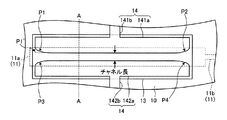
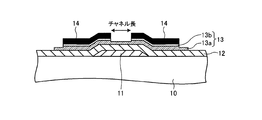
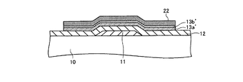
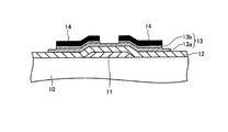
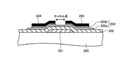
ここで、従来のバックチャネルカット(BCC)型の薄膜トランジスタについて説明する。図8および図9に従来のバックチャネルカット(BCC)型の薄膜トランジスタの構成例を示す。図8は、従来のバックチャネルカット(BCC)型の薄膜トランジスタの要部上面図であり、図9は、該薄膜トランジスタのチャネル長方向の要部断面図である。 Here, a conventional back channel cut (BCC) type thin film transistor will be described. 8 and 9 show a configuration example of a conventional back channel cut (BCC) type thin film transistor. FIG. 8 is a top view of the main part of a conventional back channel cut (BCC) type thin film transistor, and FIG. 9 is a cross-sectional view of the main part of the thin film transistor in the channel length direction.
図8および図9に示した薄膜トランジスタは、基板200と、ゲート層201と、ゲート絶縁膜202と、チャネル層203と、ソース・ドレイン層204とを備えて構成されている。ゲート層201は任意の材料からなる導体層であり、ゲート電極とこれにつながる配線とを構成する。ゲート絶縁膜202は、任意の材料からなる絶縁層であり、ゲート層201とチャネル層203との間の絶縁を行う。
The thin film transistor shown in FIGS. 8 and 9 includes a
チャネル層203は半導体層であり、一般にアモルファスシリコン(非晶質ケイ素、以下a−Siと称する)またはポリシリコン(多結晶ケイ素)により形成する。ここでは、チャネル層203としてa−Siにより形成する場合について説明する。また、チャネル層203は、第1チャネル層(真性半導体層)203aと、第2チャネル層(ドープ半導体層)203bとの積層構造により構成されている。
The
ソース・ドレイン層204は任意の材料からなる導体層であり、ソース電極、ドレイン電極、およびこれらにつながる配線を構成する。チャネル層203のうち、ソース・ドレイン層204と接する部分は、n型またはp型半導体になるようドープされた第2チャネル層203bである。なお、ゲート層201とチャネル層203との間にはゲート絶縁膜202が存在するが、薄膜トランジスタが形成された基板200上に一様に形成されているので図9においては図示していない。
The source /
以上のように構成された従来の薄膜トランジスタにおいて電流は半導体層であるチャネル層203をチャネル長方向に流れる。
In the conventional thin film transistor configured as described above, a current flows in the channel length direction through the
ところで、薄膜トランジスタは、流れた累積の電流量に応じてチャネル層の導電性が経年劣化することが知られている。このチャネル層の導電性の劣化は、チャネル層203をアモルファスシリコン(a−Si)により形成した場合に特に顕著となる。チャネル層の導電性が劣化した場合には閾値電圧が変動し、たとえばn型の場合にはより高いゲート電圧を印加しないと必要な電流が得られない。このようにチャネル層の導電性が劣化した場合には、ゲート電圧の補償が必要となる。
By the way, it is known that in the thin film transistor, the conductivity of the channel layer is deteriorated over time in accordance with the amount of accumulated current. This deterioration of the conductivity of the channel layer is particularly noticeable when the
図10に従来の薄膜トランジスタにおけるチャネル層の電流密度を示す。図10においては、H1、H2、H3、H4の部分を中心として電流密度が高く、H1〜H4よりも外側の曲線に囲まれた領域ほど電流密度が低くなっていることを示す。すなわち、図10に示すようにH1、H2、H3、H4の部分に電流集中、すなわち電流密度の極端な上昇が見られる。これは、図8においては、ソース・ドレイン層204におけるゲート層(電極)201と重なった領域で、チャネルを挟んで対向して位置する角部の近傍に対応する。この電流集中が生じているソース・ドレイン層204の角部の近傍においては、該電流集中により部分的に導電性の経年劣化が激しく進む。
FIG. 10 shows the current density of the channel layer in the conventional thin film transistor. FIG. 10 shows that the current density is high around the portions H1, H2, H3, and H4, and that the current density is lower in the region surrounded by the curve outside H1 to H4. That is, as shown in FIG. 10, current concentration, that is, an extreme increase in current density is observed in the portions H1, H2, H3, and H4. In FIG. 8, this corresponds to the vicinity of the corner located opposite to each other across the channel in the region overlapping the gate layer (electrode) 201 in the source /
チャネル層203内の電流密度が均一である場合には、該チャネル層203の導電性の劣化も部位によらず均一となるため、しきい電圧検出(たとえば、R. M. A. Dawson, et al. (1998). Design of an Improved Pixel for a Polysilicon Active-Matrix Organic LED Display. SID98 Digest, pp.11-14.参照)などの手法により対処することができる。一方、チャネル層203内の電流密度が不均一である場合には、該チャネル層203の導電性の劣化も不均一になる。そして、しきい電圧検出値にずれを生じるため、チャネル層203の導電性の劣化に応じた適正なゲート電圧の補償を行うことができない。その結果、薄膜トランジスタは、適正な電流が得られず、正常な動作ができなくなるという問題がある。このため、チャネル層203内においては電流密度が極力均一であることが求められる。
When the current density in the
このような経年劣化に対処する技術として、中心付近に配設されたソース/ドレイン領域と、ソース/ドレイン領域の外周に接触し、ソース/ドレイン領域の外周を覆うよう配設された半導体層と、半導体層の外周に接触し、半導体層の外周を覆うよう配設され、ソース/ドレイン領域の電位よりも高電位の状態に維持されたソース/ドレイン領域を備え、また、ソース/ドレイン領域の外周と、ソース/ドレイン領域の内周とは、互いが同心円となるような形状を呈する薄膜トランジスタが提案されている(たとえば、特許文献1参照)。しかしながら、このような従来の薄膜トランジスタにおいては、経年劣化の抑制は可能であるが、比較的広い領域を必要とするため、小さい画素に配置して用いることは困難であるという問題がある。 As a technique for coping with such aged deterioration, a source / drain region disposed near the center, a semiconductor layer disposed so as to contact the outer periphery of the source / drain region and cover the outer periphery of the source / drain region, A source / drain region disposed in contact with the outer periphery of the semiconductor layer and covering the outer periphery of the semiconductor layer, and maintained at a higher potential than the potential of the source / drain region. A thin film transistor has been proposed in which the outer periphery and the inner periphery of the source / drain region have shapes that are concentric with each other (see, for example, Patent Document 1). However, such a conventional thin film transistor can suppress the deterioration over time, but requires a relatively wide area, and therefore has a problem that it is difficult to use the thin film transistor in a small pixel.
本発明は、上記に鑑みてなされたものであって、チャネル層における電流集中に起因したチャネル層の導電性の劣化を緩和するとともに、狭い領域においても対応可能な高品質な薄膜トランジスタおよびこれを用いた画像表示装置を提供することを目的とする。 The present invention has been made in view of the above, and uses a high-quality thin film transistor that can reduce deterioration in conductivity of a channel layer due to current concentration in the channel layer and can cope with a narrow region. An object of the present invention is to provide an image display apparatus.
上述した課題を解決し、目的を達成するために、本発明にかかる薄膜トランジスタは、ゲート電極と、ゲート電極上に形成されたゲート絶縁膜と、ゲート絶縁膜上に形成されたチャネル層と、チャネル層上に形成されたソース・ドレイン電極と、を備え、ソース・ドレイン電極は、チャネル幅方向の両端部が曲線形状を呈するとともに、チャネル幅方向の中央部において略等しいチャネル長を有することを特徴とする。 In order to solve the above-described problems and achieve the object, a thin film transistor according to the present invention includes a gate electrode, a gate insulating film formed on the gate electrode, a channel layer formed on the gate insulating film, and a channel. A source / drain electrode formed on the layer, wherein the source / drain electrode has a curved shape at both ends in the channel width direction and has substantially the same channel length at the center in the channel width direction. And
この発明によれば、ソース・ドレイン電極のパターン変更という簡単な手法により、チャネル層内における部分的な電流集中を緩和し、これによりチャネル層内の導電性の劣化速度のばらつきを緩和した耐久性および高精度動作に優れた薄膜トランジスタを提供可能である、という効果を奏する。 According to the present invention, a simple technique of changing the pattern of the source / drain electrodes alleviates partial current concentration in the channel layer, thereby reducing the variation in the deterioration rate of conductivity in the channel layer. In addition, it is possible to provide a thin film transistor excellent in high-precision operation.
以下に、本発明にかかる薄膜トランジスタおよび画像表示装置の実施の形態を図面に基づいて詳細に説明する。なお、本発明は以下の記述により限定されるものではなく、本発明の要旨を逸脱しない範囲において適宜変更可能である。 Embodiments of a thin film transistor and an image display device according to the present invention will be described below in detail with reference to the drawings. In addition, this invention is not limited by the following description, In the range which does not deviate from the summary of this invention, it can change suitably.
実施の形態1.
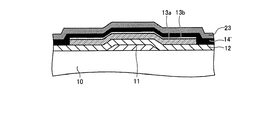
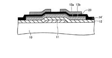
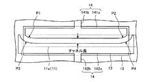
図1および図2は、本発明の実施の形態1にかかる薄膜トランジスタの構成を示す図であり、図1は実施の形態1にかかるバックチャネルカット(BCC)型の薄膜トランジスタの要部上面図であり、図2は図1の線分A−Aにおける断面図であり、実施の形態1にかかる薄膜トランジスタのチャネル長方向における要部断面図である。
Embodiment 1 FIG.
1 and 2 are diagrams showing a configuration of a thin film transistor according to a first embodiment of the present invention. FIG. 1 is a top view of a main part of a back channel cut (BCC) type thin film transistor according to the first embodiment. 2 is a cross-sectional view taken along line AA in FIG. 1, and is a cross-sectional view of the main part in the channel length direction of the thin film transistor according to the first embodiment.
本実施の形態にかかる薄膜トランジスタは、図1および図2に示すように基板10と、該基板上に形成されたゲート層11と、基板10およびゲート層11上に一様に形成されたゲート絶縁膜12と、絶縁膜12上におけるゲート層11上およびその周囲の領域に形成されたチャネル層13と、チャネル層13上に形成されたソース・ドレイン層14とを備えて構成されている。
As shown in FIGS. 1 and 2, the thin film transistor according to the present embodiment includes a
ゲート層11は任意の材料からなる導体層であり、ゲート電極11aとこれにつながる配線11bとを構成する。ゲート絶縁膜12は、任意の材料からなる絶縁層であり、ゲート層11とチャネル層13との間の絶縁を行う。チャネル層13は半導体層であり、一般にアモルファスシリコン(非晶質ケイ素、以下a−Siと称する)またはポリシリコン(多結晶ケイ素)により形成する。本実施の形態においては、チャネル層13はa−Siにより形成されているものとする。また、チャネル層13は、第1チャネル層(真性半導体層)13aと第2チャネル層(ドープ半導体層)13bとがゲート絶縁膜12側から積層された積層構造により構成されている。
The
ソース・ドレイン層14は任意の材料からなる導体層であり、ソース・ドレイン電極141a、142a、およびこれらにつながる配線141b、142bを構成する。チャネル層13のうち、ソース・ドレイン層14と接する部分は、n型またはp型半導体になるようドープされた第2チャネル層(ドープ半導体層)13bである。なお、図1に示すようにゲート層11とチャネル層13との間にはゲート絶縁膜12が形成されているが、該ゲート絶縁膜12は薄膜トランジスタが形成された基板10上に一様に形成されているので図1においては図示していない。
The source /
つぎに、本実施の形態にかかる薄膜トランジスタの特徴について説明する。本実施の形態にかかる薄膜トランジスタにおいては、一対のソース・ドレイン電極であるソース・ドレイン電極141a、142aは、図1に示すように対向するチャネル幅方向の両端部P1、P2、P3、P4が、チャネル幅方向の中央近傍におけるチャネル長以上の曲率半径で角を有さない曲線形状を呈するとともに、チャネル幅方向において前記の両端部P1、P2、P3、P4を除いて略同一(チャネル長のばらつきが±3μm以内であることが好ましい)のチャネル長を有する。なお、ソース・ドレイン電極のチャネル幅方向の両端部とは、ソース電極とドレイン電極との間に実質的に電流が流れる領域におけるチャネル幅方向の両端部のことである。一般的には、ソース・ドレイン電極のチャネル幅方向の両端部とは、ソース・ドレイン電極及びチャネル層が互いに重畳する第1重畳領域と、ゲート電極及びチャネル層が互いに重畳する第2重畳領域とがチャネル幅方向に沿って配置されている場合、第1及び第2重畳領域の双方が配置された領域におけるソース・ドレイン電極のチャネル幅方向の両端部のことをいう。
Next, features of the thin film transistor according to this embodiment will be described. In the thin film transistor according to the present embodiment, the source /
このトランジスタのチャネル層13における電流密度を図3に示す。図3においても、図10と同様に外側の曲線に囲まれた領域ほど電流密度が低くなっていることを示す。図3に示すように、従来の薄膜トランジスタのチャネル層における電流密度(図10参照)と比較して、前記のソース・ドレイン電極141a、142aの両端部P1、P2、P3、P4に電流密度の過度に高い領域がなく、電流集中が緩和されているのが分かる。薄膜トランジスタのチャネル層では、角を有する部分に電流集中が起こり、電流密度が過度に高くなる。
The current density in the
そこで、本実施の形態にかかる薄膜トランジスタにおいては、一対のソース・ドレイン電極であるソース・ドレイン電極141a、142aの対向するチャネル幅方向の両端部P1、P2、P3、P4の形状を、チャネル幅方向の中央近傍におけるチャネル長以上の曲率半径で角を有さない曲線形状とする。これにより、チャネル層13におけるP1、P2、P3、P4の部位の電流集中を緩和することができる。そして、この部分のチャネル層13における電流集中を緩和することにより、チャネル層13におけるP1、P2、P3、P4の部位の部分的な電導性の経年劣化を緩和することができる。
Therefore, in the thin film transistor according to the present embodiment, the shapes of the opposite ends P1, P2, P3, and P4 in the channel width direction of the source /
また、本実施の形態にかかる薄膜トランジスタにおいては、チャネル幅方向において前記の両端部P1、P2、P3、P4を除いて略同一のチャネル長を有する。これにより、電流密度を均一にすることができ、チャネル層13内の導電性の劣化速度のばらつきを緩和することができる。
In addition, the thin film transistor according to the present embodiment has substantially the same channel length in the channel width direction except for the both end portions P1, P2, P3, and P4. Thereby, the current density can be made uniform, and variation in the deterioration rate of the conductivity in the
また、本実施の形態にかかる薄膜トランジスタは、ソース・ドレイン電極141a、142aにおける両端部P1、P2、P3、P4の形状のみを、チャネル幅方向の中央近傍におけるチャネル長以上の曲率半径で角を有さない曲線形状としているため、広い領域を必要とせず、狭い領域においても形成が可能である。
In the thin film transistor according to the present embodiment, only the shapes of both end portions P1, P2, P3, and P4 of the source /
したがって、本実施の形態にかかる薄膜トランジスタによれば、ソース・ドレイン電極141a、142aのパターンを変更するといった簡単な手法によりチャネル層13内における部分的な電流集中を緩和し、これによりチャネル層内の導電性の劣化速度のばらつきを緩和した耐久性および高精度動作に優れた薄膜トランジスタを実現可能である。
Therefore, according to the thin film transistor according to the present embodiment, partial current concentration in the
また、本実施の形態にかかる薄膜トランジスタでは、一対のソース・ドレイン電極141a、142aが略長方形を呈し、前記のP1、P2、P3、P4部の曲線形状の一端がソース・ドレイン電極11aの短辺を起点とし、一方、前記のP1、P2、P3、P4部の曲線形状の他端がソース・ドレイン電極141aの長辺を起点としている。そして、ソース・ドレイン電極141a、142aの長辺と短辺との仮想交点(たとえば、図1に示すP1′)と曲線形状の他端との間の距離Lがチャネル幅方向のチャネル中央近傍におけるチャネル長の2倍以下とされている。これにより、ソース・ドレイン電極141a、142aの両端部に曲線形状を設けることによるチャネル幅の減少を良好に抑制することができる。
In the thin film transistor according to the present embodiment, the pair of source /
なお、このようなソース・ドレイン層14は、ソース・ドレイン層14の形状パターンの変更により実現できるため、既存の製造工程や部材に大きな影響を及ぼすこと無く実現することができる。
In addition, since such a source /
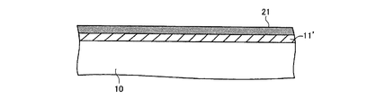
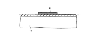
つぎに、上述した本実施の形態にかかる薄膜トランジスタの製造方法について説明する。まず、図4−1に示すように、ガラス等の基板10上にゲート層11を形成するための金属層11′を形成する。金属層11′は、タンタル(Ta)、チタン(Ti)、アルミニウム(Al)、クロム(Cr)、銅(Cu)などの単層または多層の金属をスパッタリング法などにより堆積して形成される。つぎに、図4−1に示すようにレジスト21を塗布し、図4−2に示すようにパターニングする。
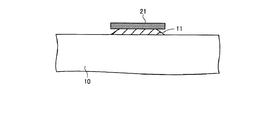
Next, a manufacturing method of the thin film transistor according to the above-described embodiment will be described. First, as shown in FIG. 4A, a
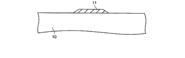
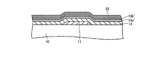
つぎに、パターニングしたレジスト21をマスクに用いて金属層11′のエッチングを行って図4−3に示すようにゲート層11を形成し、レジスト21を除去する。図4−4にレジスト除去後の状態を示す。つぎに、図4−5に示すようにゲート絶縁膜12としてシリコン窒化膜12、第1チャネル層13a用のアモルファスシリコン膜(真性半導体膜)13a′、第2チャネル層13b用のドープアモルファスシリコン膜(ドープ半導体膜)13b′をこの順で基板10上およびゲート層11上に形成する。シリコン窒化膜12′は、たとえばプラズマCVD法またはスパッタリング法などによって単層または多層に形成することができる。また、アモルファスシリコン膜(真性半導体膜)13a′およびドープアモルファスシリコン膜(ドープ半導体膜)13b′はたとえばプラズマCVD法によって形成することができる。
Next, the
つぎに、図4−5に示すようにレジスト22を塗布し、図4−6に示すようにパターニングする。そして、パターニングしたレジスト22をマスクに用いて第2チャネル層13b用のドープアモルファスシリコン膜(ドープ半導体膜)13b′および第1チャネル層13a用のアモルファスシリコン膜(真性半導体膜)13a′のエッチングを行って図4−7に示すように第1チャネル層(真性半導体層)13aと第2チャネル層(ドープ半導体層)13bとを形成し、レジスト22を除去する。図4−8にレジスト除去後の状態を示す。
Next, a resist 22 is applied as shown in FIG. 4-5 and patterned as shown in FIG. 4-6. Then, using the patterned resist 22 as a mask, the doped amorphous silicon film (doped semiconductor film) 13b ′ for the
つぎに、図4−9に示すようにソース・ドレイン層14用の金属層14′を堆積し、レジスト23を塗布し、図4−10に示すようにレジスト23をパターニングする。この金属層は、たとえばスパッタリング法などによって形成することができ、アルミニウム、チタン、珪化モリブデン、ITO等を単層または多層に堆積して形成することができる。そして、パターニングしたレジスト23をマスクに用いて図4−11に示すように金属層14′のエッチングを行ってソース・ドレイン層14を形成する。このとき、図1に示すようにソース・ドレイン層14の端部P1、P2、P3、P4を曲線形状に形成する。さらに図4−12に示すように第2チャネル層(ドープ半導体層)13bのエッチングを行ってパターニングをし、レジスト23を除去する。図4−13にレジスト除去後の状態を示す。以上により、図1および図2に示した本実施の形態にかかる薄膜トランジスタが完成する。
Next, a metal layer 14 'for the source /
なお、たとえば特開2005−72135号公報にはソース・ドレイン電極の形状を変化させた薄膜トランジスタが示されているが、本発明は以下の点で大きく異なるものである。同文献に示された薄膜トランジスタは光リークを軽減するためチャネル端におけるチャネル長を大きくするものであるが、同文献に示された薄膜トランジスタは本発明の目的を満足するものではない。すなわち、同文献の図1の薄膜トランジスタはソース・ドレイン電極の端に135°前後の頂点があり、この頂点で電流集中が起きる。また、図5の薄膜トランジスタはチャネル中央のチャネル長が均一でないため、電流密度が不均一になる。また、図10、図11、図12、図13の薄膜トランジスタは直角の頂点を有しており、この頂点で電流集中が起きる。したがって、これらの薄膜トランジスタでは、本発明の効果を得られるものではない。 For example, Japanese Patent Application Laid-Open No. 2005-72135 discloses a thin film transistor in which the shape of the source / drain electrodes is changed. However, the present invention is greatly different in the following points. The thin film transistor disclosed in this document increases the channel length at the channel end in order to reduce light leakage, but the thin film transistor disclosed in this document does not satisfy the object of the present invention. That is, the thin film transistor of FIG. 1 of the same document has a vertex of about 135 ° at the end of the source / drain electrode, and current concentration occurs at this vertex. Further, since the channel length at the center of the channel is not uniform in the thin film transistor of FIG. 5, the current density is not uniform. 10, 11, 12, and 13 have a right apex, and current concentration occurs at this apex. Therefore, the effects of the present invention cannot be obtained with these thin film transistors.
実施の形態2.
実施の形態2においては、本発明にかかる薄膜トランジスタの変形例について説明する。図5は、本発明の実施の形態2にかかる薄膜トランジスタの構成を示す図であり、バックチャネルカット(BCC)型の薄膜トランジスタの要部上面図である。本実施の形態にかかる薄膜トランジスタの基本構成は、上述した実施の形態1にかかる薄膜トランジスタと同様であるため、同じ部材については図1と同じ符号を付すことでここでは詳細な説明は省略する。
Embodiment 2. FIG.
In the second embodiment, a modification of the thin film transistor according to the present invention will be described. FIG. 5 is a diagram showing the configuration of the thin film transistor according to the second embodiment of the present invention, and is a top view of the main part of the back channel cut (BCC) type thin film transistor. Since the basic configuration of the thin film transistor according to the present embodiment is the same as that of the thin film transistor according to the first embodiment described above, the same members are denoted by the same reference numerals as those in FIG.
本実施の形態にかかる薄膜トランジスタが実施の形態1にかかる薄膜トランジスタと異なる点は、ソース・ドレイン電極141a、142aのうち、ソース電極とドレイン電極との間に実質的に電流が流れる領域、すなわちソース・ドレイン電極141a、142aがチャネル層と重なる領域において対向するチャネル幅方向の両端部P3、P4が、両端部P1、P2の曲率半径よりも大とされた凹形状とされている点である。
The thin film transistor according to the present embodiment is different from the thin film transistor according to the first embodiment in that a region where a current substantially flows between the source electrode and the drain electrode in the source /
本発明においては、チャネル層上のソース・ドレイン電極の曲率半径がチャネル長以上であれば良く、チャネル幅方向の両端でチャネル長が大きい必要はなく、またソース・ドレイン電極形状が凸形状である必要もない。ただし、チャネル幅方向における両端でのチャネル長がチャネル幅方向中央でのチャネル長より小さくなることは、電流密度が高くなることにつながるので好ましくない。 In the present invention, the radius of curvature of the source / drain electrodes on the channel layer may be equal to or greater than the channel length, the channel length need not be large at both ends in the channel width direction, and the source / drain electrode shape is convex. There is no need. However, it is not preferable that the channel length at both ends in the channel width direction is smaller than the channel length at the center in the channel width direction because the current density is increased.
したがって、本実施の形態にかかる薄膜トランジスタにおいても上述した実施の形態1にかかる薄膜トランジスタと同様の効果を得ることができる。 Therefore, also in the thin film transistor according to the present embodiment, the same effect as the thin film transistor according to the first embodiment described above can be obtained.
実施の形態3.
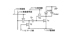
実施の形態3では、上述した本発明にかかる薄膜トランジスタを適用した画像表示装置について説明する。図6は、上述した本発明を適用した薄膜トランジスタ(n−MISFET TFT)を用いて構成した有機EL表示装置の1画素に対応する画素回路の構成を示す図である。同図において、画素回路は、注入電流に応じた輝度で発光する発光手段として有機EL素子OLEDを、発光手段である有機EL素子OLEDへの注入電流を制御する制御手段として有機EL素子容量Coled、駆動トランジスタTd、閾値電圧検出用トランジスタTth、補助容量Cs、スイッチングトランジスタTsおよびスイッチングトランジスタTmを、備えて構成されている。
Embodiment 3 FIG.
In Embodiment 3, an image display device to which the above-described thin film transistor according to the present invention is applied will be described. FIG. 6 is a diagram showing a configuration of a pixel circuit corresponding to one pixel of an organic EL display device configured by using the above-described thin film transistor (n-MISFET TFT) to which the present invention is applied. In the figure, the pixel circuit includes an organic EL element OLED as a light emitting means that emits light with a luminance corresponding to the injection current, and an organic EL element capacitance Coled as a control means for controlling an injection current to the organic EL element OLED that is a light emitting means. The driving transistor Td, the threshold voltage detecting transistor Tth, the auxiliary capacitor Cs, the switching transistor Ts, and the switching transistor Tm are provided.
有機EL素子OLEDは、閾値電圧以上の電位差(アノード−カソード間電位差)が生じることにより、電流が流れ、発光する特性を有する素子である。具体的には、有機EL素子OLEDは、Al、Cu、ITO(Indium Tin Oxide)等によって形成されたアノード層およびカソード層と、アノード層とカソード層との間にフタルシアニン、トリスアルミニウム錯体、ベンゾキノリノラト、ベリリウム錯体等の有機系の材料によって形成された発光層とを少なくとも備えた構造を有し、発光層に注入された正孔と電子とが発光再結合することによって光を生じる機能を有する。有機EL素子容量Coledは、有機EL素子OLEDの容量を等価的に表したものである。 The organic EL element OLED is an element having a characteristic that a current flows and emits light when a potential difference (anode-cathode potential difference) equal to or higher than a threshold voltage is generated. Specifically, the organic EL element OLED includes an anode layer and a cathode layer formed of Al, Cu, ITO (Indium Tin Oxide), and the like, and a phthalocyanine, trisaluminum complex, benzoate between the anode layer and the cathode layer. It has a structure including at least a light emitting layer formed of an organic material such as quinolinolato or beryllium complex, and generates light by recombination of holes and electrons injected into the light emitting layer. Have The organic EL element capacity Coled is an equivalent expression of the capacity of the organic EL element OLED.
駆動トランジスタTdは、ゲート電極・ソース電極間に与えられる電位差に応じて有機EL素子OLEDに流れる電流量を制御するためのものである。また閾値電圧検出用トランジスタTthは、オン状態となった時に、駆動トランジスタTdのゲート電極とドレイン電極とを電気的に接続し、駆動トランジスタTdのゲート電極・ソース電極間の電位差が駆動トランジスタTdの閾値電圧Vthとなるまで駆動トランジスタTdのゲート電極からドレイン電極に向かって電流を流すことにより、駆動トランジスタTdの閾値電圧Vthを検出する機能を有している。 The drive transistor Td is for controlling the amount of current flowing through the organic EL element OLED according to the potential difference applied between the gate electrode and the source electrode. Further, when the threshold voltage detection transistor Tth is turned on, the gate electrode and the drain electrode of the drive transistor Td are electrically connected, and the potential difference between the gate electrode and the source electrode of the drive transistor Td is increased. It has a function of detecting the threshold voltage Vth of the drive transistor Td by causing a current to flow from the gate electrode to the drain electrode of the drive transistor Td until the threshold voltage Vth is reached.
駆動トランジスタTd、閾値電圧検出用トランジスタTth、スイッチングトランジスタTsおよびスイッチングトランジスタTmは、薄膜トランジスタである。そして、有機EL素子OLEDに直接接続されて該有機EL素子OLEDの駆動を制御する駆動トランジスタTdに関しては、上述した本発明にかかる薄膜トランジスタを用いている。 The drive transistor Td, the threshold voltage detection transistor Tth, the switching transistor Ts, and the switching transistor Tm are thin film transistors. As the drive transistor Td that is directly connected to the organic EL element OLED and controls the drive of the organic EL element OLED, the above-described thin film transistor according to the present invention is used.
電源線110は、駆動トランジスタTdおよびスイッチングトランジスタTmに電源を供給する。Tth制御線111は、閾値電圧検出用トランジスタTthを制御するための信号を供給する。マージ線112は、スイッチングトランジスタTmを制御するための信号を供給する。走査線113は、スイッチングトランジスタTsを制御するための信号を供給する。画像信号線114は、画像信号を供給する。
The power line 110 supplies power to the drive transistor Td and the switching transistor Tm. The
上記構成において、画素回路は、準備期間、閾値電圧検出期間、書き込み期間および発光期間という4つの期間を経て動作する。すなわち、準備期間では、電源線110には所定の正電位(Vp、Vp>0)が引加され、閾値電圧検出用トランジスタTthがオフ、スイッチングトランジスタTsがオフ、駆動トランジスタTdがオン、スイッチングトランジスタTmがオンとなるように制御される。その結果、電源線110→駆動トランジスタTd→有機EL素子容量Coledという経路で電流が流れ、有機EL素子容量Coledに電荷が蓄積される。 In the above structure, the pixel circuit operates through four periods of a preparation period, a threshold voltage detection period, a writing period, and a light emission period. That is, in the preparation period, a predetermined positive potential (Vp, Vp> 0) is applied to the power supply line 110, the threshold voltage detection transistor Tth is turned off, the switching transistor Ts is turned off, the drive transistor Td is turned on, and the switching transistor Control is performed so that Tm is turned on. As a result, a current flows through a path of the power supply line 110 → the driving transistor Td → the organic EL element capacitor Coled, and charges are accumulated in the organic EL element capacitor Coled.
つぎの閾値電圧検出期間では、電源線110にはゼロ電位が印加され、閾値電圧検出用トランジスタTthがオンとなるように制御され、駆動トランジスタTdのゲートとドレインとが接続される。これにより、補助容量Csおよび有機EL素子容量Coledに蓄積された電荷が放電され、駆動トランジスタTd→電源線110という経路で電流が流れる。そして、駆動トランジスタTdのゲート−ドレイン間の電位差が、駆動トランジスタTdの駆動閾値に対応する閾値電圧Vthに達すると、駆動トランジスタTdがオフとされる。 In the next threshold voltage detection period, a zero potential is applied to the power supply line 110, the threshold voltage detection transistor Tth is controlled to be turned on, and the gate and drain of the drive transistor Td are connected. As a result, the charges accumulated in the auxiliary capacitor Cs and the organic EL element capacitor Coled are discharged, and a current flows through the path of the drive transistor Td → the power supply line 110. When the potential difference between the gate and the drain of the drive transistor Td reaches the threshold voltage Vth corresponding to the drive threshold of the drive transistor Td, the drive transistor Td is turned off.
つぎの書き込み期間では、電源線110の電位はゼロ電位を維持し、スイッチングトランジスタTsがオン、スイッチングトランジスタTmがオフとなり、有機EL素子容量Coledに蓄積された電荷が放電される。その結果、有機EL素子容量Coled→閾値電圧検出用トランジスタTth→補助容量Csという経路で電流が流れ、補助容量Csに電荷が蓄積される。すなわち、有機EL素子容量Coledに蓄積された電荷は、補助容量Csに移動する。 In the next writing period, the potential of the power supply line 110 maintains zero potential, the switching transistor Ts is turned on, the switching transistor Tm is turned off, and the charge accumulated in the organic EL element capacitor Coled is discharged. As a result, a current flows through a path of organic EL element capacitance Coled → threshold voltage detection transistor Tth → auxiliary capacitance Cs, and charges are accumulated in the auxiliary capacitance Cs. That is, the charge accumulated in the organic EL element capacitor Coled moves to the auxiliary capacitor Cs.
つぎの発光期間では、電源線110には所定の負電位(−VDD、VDD>0)が引加され、駆動トランジスタTdがオン、閾値電圧検出用トランジスタTthがオフ、スイッチングトランジスタTsがオフとなるように制御される。その結果、有機EL素子OLED→駆動トランジスタTd→電源線110という経路で電流が流れ、有機EL素子OLEDが発光する。 In the next light emission period, a predetermined negative potential (−VDD, VDD> 0) is applied to the power supply line 110, the drive transistor Td is turned on, the threshold voltage detection transistor Tth is turned off, and the switching transistor Ts is turned off. To be controlled. As a result, a current flows through a path of the organic EL element OLED → the driving transistor Td → the power supply line 110, and the organic EL element OLED emits light.
以上のような本実施の形態にかかる有機EL表示装置においては、駆動トランジスタTdに本発明にかかる薄膜トランジスタを用いているため、省スペース化(小型化)を実現するとともに、電流集中に起因したチャネル層の部分的な経年劣化を緩和した耐久性と高精度動作に優れた有機EL表示装置が実現されている。 In the organic EL display device according to the present embodiment as described above, since the thin film transistor according to the present invention is used for the drive transistor Td, a space saving (miniaturization) is realized and a channel caused by current concentration is provided. An organic EL display device excellent in durability and high-precision operation in which partial aging of the layer is alleviated has been realized.
ここで、本実施の形態にかかる有機EL表示装置においては、駆動トランジスタTdのみに限定して、本発明にかかる薄膜トランジスタを用いている。本発明にかかる薄膜トランジスタは、実質的に電流が流れる領域におけるソース・ドレイン電極の端部の形状を、曲線により構成するため、わずかであるがチャネル幅が必要最少寸法よりも大きくなる。したがって、有機EL表示装置に用いるすべての薄膜トランジスタに本発明にかかる薄膜トランジスタを用いた場合には、薄膜トランジスタの使用領域が多少大きくなる虞がある。 Here, in the organic EL display device according to the present embodiment, the thin film transistor according to the present invention is used only for the drive transistor Td. In the thin film transistor according to the present invention, since the shape of the end of the source / drain electrode in the region where the current substantially flows is configured by a curve, the channel width is slightly larger than the necessary minimum dimension. Therefore, when the thin film transistor according to the present invention is used for all the thin film transistors used in the organic EL display device, there is a possibility that the use area of the thin film transistor becomes somewhat large.
そこで、極力画素領域を省スペース化(小型化)したい場合には、電流集中によるチャネル層の劣化が直接画像表示に悪影響を及ぼす駆動トランジスタTdのみに限定して、本発明にかかる薄膜トランジスタを用いることが好ましい。これにより、本実施の形態にかかる有機EL表示装置のように、小型化を実現するとともに、電流集中に起因したチャネル層の部分的な経年劣化を緩和した耐久性と高精度動作に優れた有機EL表示装置を実現することができる。なお、有機EL表示装置に備える他の薄膜トランジスタに本発明にかかる薄膜トランジスタを適用することも可能である。 Therefore, when it is desired to save the pixel area as much as possible (miniaturization), the thin film transistor according to the present invention is used only for the drive transistor Td in which deterioration of the channel layer due to current concentration directly affects the image display. Is preferred. As a result, as with the organic EL display device according to the present embodiment, the organic EL display device is miniaturized and has excellent durability and high-precision operation with reduced partial aging of the channel layer due to current concentration. An EL display device can be realized. Note that the thin film transistor according to the present invention can be applied to other thin film transistors included in the organic EL display device.
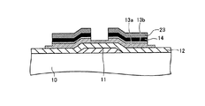
なお、本発明は上述の実施形態に限定されるものではなく、本発明の範囲を逸脱しない範囲内で種々の変更・改良が可能である。例えば、上述の実施形態においては、本発明を、ゲート電極がソース・ドレイン電極よりも基板側に位置するボトム・ゲート構造の薄膜トランジスタに適用した場合について説明したが、これに代えて、図8に示すように、ソース・ドレイン電極がゲート電極よりも基板側に位置するトップ・ゲート構造の薄膜トランジスタに適用しても良い。 In addition, this invention is not limited to the above-mentioned embodiment, A various change and improvement are possible within the range which does not deviate from the scope of this invention. For example, in the above-described embodiment, the case where the present invention is applied to a bottom-gate thin film transistor in which the gate electrode is located on the substrate side with respect to the source / drain electrode has been described. As shown, the thin film transistor may be applied to a top-gate thin film transistor in which the source / drain electrodes are located on the substrate side of the gate electrode.
以上のように、本発明にかかる薄膜トランジスタは、画像表示装置の小型化された画素の駆動用に有用であり、特に、耐久性と高精度動作が要求される用途に適している。 As described above, the thin film transistor according to the present invention is useful for driving a downsized pixel of an image display device, and is particularly suitable for an application that requires durability and high-precision operation.
10 基板
11 ゲート層
11a ゲート電極
11b 配線
12 ゲート絶縁膜
13 チャネル層
13a 第1チャネル層(真性半導体層)
13b 第2チャネル層(ドープ半導体層)
14 ソース・ドレイン層
110 電源線
111 制御線
112 マージ線
113 走査線
114 画像信号線
141a ソース・ドレイン電極
141b 配線
142b ソース・ドレイン電極
142b 配線
200 基板
201 ゲート層
202 絶縁膜
203 チャネル層
203b チャネル層
203 チャネル層
203 該チャネル層
204 ソース・ドレイン層
Coled 素子容量
Cs 補助容量
EL 有機
OLED 素子
Td 駆動トランジスタ
Tm スイッチングトランジスタ
Ts スイッチングトランジスタ
Tth 閾値電圧検出用トランジスタ
Vth 閾値電圧
DESCRIPTION OF
13b Second channel layer (doped semiconductor layer)
14 Source / Drain Layer 110
Claims (5)
前記ゲート電極上に形成されたゲート絶縁膜と、
前記ゲート絶縁膜上に形成されたチャネル層と、
前記チャネル層上に形成されたソース・ドレイン電極と、
を備え、
前記ソース・ドレイン電極は、チャネル幅方向の両端部が曲線形状を呈するとともに、前記チャネル幅方向の中央部において略等しいチャネル長を有すること
を特徴とする薄膜トランジスタ。 A gate electrode;
A gate insulating film formed on the gate electrode;
A channel layer formed on the gate insulating film;
Source / drain electrodes formed on the channel layer;
With
The source / drain electrodes have a curved shape at both ends in the channel width direction, and have substantially the same channel length at the center in the channel width direction.
を特徴とする請求項1に記載の薄膜トランジスタ。 2. The thin film transistor according to claim 1, wherein a radius of curvature of the both end portions in the channel width direction of the source / drain electrodes is equal to or greater than a channel length in the central portion of the source / drain electrodes in the channel width direction.
前記曲線形状の他端から前記ソース・ドレイン電極の前記第1辺及び前記第2辺との仮想交点までの距離が前記チャネル幅方向の中央部におけるチャネル長の2倍以下であること
を特徴とする請求項1または請求項2に記載の薄膜トランジスタ。 The source / drain electrodes have a substantially quadrilateral shape having a first side substantially parallel to the channel length direction and a second side substantially parallel to the channel width direction, and one end of the curved shape is the one of the source / drain electrodes. The first side is the other end of the curved shape starting from the second side of the source / drain electrode,
The distance from the other end of the curved shape to the virtual intersection of the first and second sides of the source / drain electrode is not more than twice the channel length at the center in the channel width direction. The thin film transistor according to claim 1 or 2.
を特徴とする請求項1乃至請求項3のいずれか1つに記載の薄膜トランジスタ。 The both end portions of the source / drain electrode are both end portions in the channel width direction in a region where a current substantially flows between the source electrode and the drain electrode. The thin-film transistor as described in any one.
各前記画素は、
注入電流に応じた輝度で発光する発光手段と、
前記発光手段を駆動する駆動トランジスタを含む複数のトランジスタと、
を備え、
複数の前記トランジスタのうち、前記駆動トランジスタのみが請求項1乃至4のいずれか1つに記載の薄膜トランジスタであること
を特徴とする画像表示装置。 In an image display device having a plurality of pixels,
Each said pixel is
A light emitting means for emitting light at a luminance according to the injected current;
A plurality of transistors including a driving transistor for driving the light emitting means;
With
5. The image display device according to claim 1, wherein only the driving transistor among the plurality of transistors is the thin film transistor according to claim 1.
Priority Applications (1)
| Application Number | Priority Date | Filing Date | Title |
|---|---|---|---|
| JP2005317044A JP2007123732A (en) | 2005-10-31 | 2005-10-31 | Thin film transistor and image display device |
Applications Claiming Priority (1)
| Application Number | Priority Date | Filing Date | Title |
|---|---|---|---|
| JP2005317044A JP2007123732A (en) | 2005-10-31 | 2005-10-31 | Thin film transistor and image display device |
Publications (1)
| Publication Number | Publication Date |
|---|---|
| JP2007123732A true JP2007123732A (en) | 2007-05-17 |
Family
ID=38147213
Family Applications (1)
| Application Number | Title | Priority Date | Filing Date |
|---|---|---|---|
| JP2005317044A Pending JP2007123732A (en) | 2005-10-31 | 2005-10-31 | Thin film transistor and image display device |
Country Status (1)
| Country | Link |
|---|---|
| JP (1) | JP2007123732A (en) |
Cited By (1)
| Publication number | Priority date | Publication date | Assignee | Title |
|---|---|---|---|---|
| CN115966572A (en) * | 2021-10-12 | 2023-04-14 | 乐金显示有限公司 | Thin film transistor and display device including the same |
-
2005
- 2005-10-31 JP JP2005317044A patent/JP2007123732A/en active Pending
Cited By (2)
| Publication number | Priority date | Publication date | Assignee | Title |
|---|---|---|---|---|
| CN115966572A (en) * | 2021-10-12 | 2023-04-14 | 乐金显示有限公司 | Thin film transistor and display device including the same |
| US12538526B2 (en) | 2021-10-12 | 2026-01-27 | Lg Display Co., Ltd. | Thin film transistor and display device comprising the same |
Similar Documents
| Publication | Publication Date | Title |
|---|---|---|
| US9257493B2 (en) | Organic light-emitting diode display device | |
| US7683382B2 (en) | Organic light emitting diode display | |
| USRE48032E1 (en) | Thin-film semiconductor substrate, light-emitting panel, and method of manufacturing the thin-film semiconductor substrate | |
| JP5096437B2 (en) | Organic EL display device | |
| US20070075955A1 (en) | Organic light emitting diode display | |
| WO2018180617A1 (en) | Active matrix substrate, liquid crystal display device, and organic el display device | |
| US8013325B2 (en) | Thin film transistor, organic light emitting device including thin film transistor, and manufacturing method thereof | |
| US20090075440A1 (en) | Display and manufacturing method thereof | |
| US7863602B2 (en) | Organic light emitting diode display and method for manufacturing the same | |
| JPWO2011161910A1 (en) | Light emitting display device and manufacturing method thereof | |
| US7038240B2 (en) | Color display device | |
| CN101414610B (en) | Display unit and manufacturing method of the display unit | |
| JP2009043748A (en) | Semiconductor device and electro-optical device | |
| TW201411853A (en) | Thin film transistor and manufacturing method thereof, and display unit and electronic device | |
| KR100740132B1 (en) | Organic electroluminescent display | |
| WO2019187102A1 (en) | Active matrix substrate, display device, and active matrix substrate manufacturing method | |
| US10868098B2 (en) | OLED display panel and OLED display | |
| JP2007123732A (en) | Thin film transistor and image display device | |
| KR20140028604A (en) | Organic light emitting diode display device and method of fabricating the same | |
| JP2007142324A (en) | Thin film transistor and image display device | |
| US8525176B2 (en) | Thin film transistor, display device using the same, and thin film transistor manufacturing method | |
| KR20040078560A (en) | Electro luminescence display device | |
| KR102388241B1 (en) | Display panel and display panel including the same and driving method thereof | |
| US11710746B2 (en) | Semiconductor device and display device | |
| US20240290278A1 (en) | Display device |