JP2007114231A - Liquid crystal lens - Google Patents
Liquid crystal lens Download PDFInfo
- Publication number
- JP2007114231A JP2007114231A JP2005302351A JP2005302351A JP2007114231A JP 2007114231 A JP2007114231 A JP 2007114231A JP 2005302351 A JP2005302351 A JP 2005302351A JP 2005302351 A JP2005302351 A JP 2005302351A JP 2007114231 A JP2007114231 A JP 2007114231A
- Authority
- JP
- Japan
- Prior art keywords
- lens
- liquid crystal
- substrate
- electrode
- layer
- Prior art date
- Legal status (The legal status is an assumption and is not a legal conclusion. Google has not performed a legal analysis and makes no representation as to the accuracy of the status listed.)
- Pending
Links
Images


Abstract
Description
本発明は、外部電圧により焦点距離を変えることの可能な液晶レンズに関する。 The present invention relates to a liquid crystal lens capable of changing a focal length by an external voltage.
液晶は、液体のような流動性を有し、電気的光学的特性に異方性を示し、かつ分子配向状態を種々制御できるという特徴を有している。かかる液晶の特徴を利用した液晶表示素子は、薄型の平板型表示素子として、近年、目覚しい発展を続けている。 The liquid crystal has fluidity like a liquid, has anisotropy in electro-optical characteristics, and can control various molecular orientation states. In recent years, liquid crystal display elements utilizing the characteristics of liquid crystals have been remarkably developed as thin flat panel display elements.
液晶分子の配向状態は、液晶表示素子を構成する2枚の透明導電膜を付したガラス基板の表面の処理や、外部印可電圧により容易に制御することができるので、液晶は、電圧印可により実効的な屈折率を異常光に対する値から常光に対する値まで連続的に可変できるという、他の光学材料にない優れた特性を有している。 The alignment state of the liquid crystal molecules can be easily controlled by the treatment of the surface of the glass substrate provided with the two transparent conductive films constituting the liquid crystal display element and the external applied voltage. It has an excellent characteristic that other optical materials do not have such that the refractive index can be continuously varied from the value for extraordinary light to the value for ordinary light.
このような液晶を用いた光学素子は、通常の受動型の光学素子とは異なり、媒質である液晶の屈折率を電圧印可により比較的容易に可変制御できるため、焦点距離を可変できる液晶レンズとして実現することができる。 An optical element using such a liquid crystal, unlike a normal passive optical element, can be variably controlled by applying a voltage to the refractive index of the liquid crystal, which is a medium. Can be realized.
例えば、ガラス基板と平凸レンズの間に液晶材料を挟み、平凸レンズの平面側を一方のガラス基板に接するように配置し、平凸レンズの曲面側に電極を設ける液晶レンズが提案されている(例えば、特許文献1参照。)。この液晶レンズは、上述した形状を備えることにより、簡単な構成できわめて容易に光学的特性を可変することができるようになっている。 For example, a liquid crystal lens has been proposed in which a liquid crystal material is sandwiched between a glass substrate and a plano-convex lens, the plane side of the plano-convex lens is placed in contact with one glass substrate, and an electrode is provided on the curved surface side of the plano-convex lens (for example, , See Patent Document 1). Since this liquid crystal lens has the shape described above, the optical characteristics can be varied very easily with a simple configuration.
しかしながら、上述した液晶レンズにおいては、平板状のガラス基板と平凸レンズの間に液晶材料を挟むことになるので、従来の量産生産方式が使えず、量産性が低いという問題がある。 However, in the above-described liquid crystal lens, a liquid crystal material is sandwiched between a flat glass substrate and a plano-convex lens. Therefore, there is a problem that the conventional mass production method cannot be used and the mass productivity is low.
また、2枚の平板ガラス基板に液晶材料を挟むタイプの液晶レンズにおいては、液晶材料中の電位分布を示す電位分布曲線が比較的緩やかな曲線となることが知られており、このため、焦点距離が比較的長くなってしまうという問題がある。 In addition, in a liquid crystal lens of a type in which a liquid crystal material is sandwiched between two flat glass substrates, it is known that a potential distribution curve indicating a potential distribution in the liquid crystal material is a relatively gentle curve. There is a problem that the distance becomes relatively long.
本発明は、上記の問題を解決するためになされたものであり、その課題の一例としては、量産性に優れるとともに、短焦点距離化が可能な液晶レンズを提供することにある。 The present invention has been made to solve the above problems, and an example of the problem is to provide a liquid crystal lens that is excellent in mass productivity and capable of shortening the focal length.
上記の課題を達成するため、請求項1記載の液晶レンズは、第1の電極を備える第1の平板形状の基板と、前記第1の平板形状の基板と対向し、第2の電極を備える第2の平板形状の基板と、前記第1の平板形状の基板と前記第2の平板形状の基板に挟まれ、前記第1の電極と前記第2の電極との間に加えられる電圧に応じて屈折率が変化する液晶層と、を有し、前記第1の平板形状の基板及び前記第2の平板形状の基板の少なくともいずれか一方は、平板形状のレンズであることを特徴とする。
In order to achieve the above object, a liquid crystal lens according to
以下、本発明の実施の形態を図面を用いて説明する。 Hereinafter, embodiments of the present invention will be described with reference to the drawings.
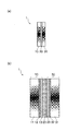
図1は、本発明の実施の形態に係る液晶レンズ1の概略構成を示す断面図である。図1(a)に示すように、液晶レンズ1は、第1電極を有する第1基板層10、第2電極を有する第2基板層30、及び第1基板層10と第2基板層30の間に挟まれた液晶層20を備える構成である。ここで、液晶レンズ1の第1基板層10及び第2基板層30は、平板形状の固定レンズ領域を具備し、固定レンズ領域は、例えば、屈折率分布レンズ(GRINレンズ)や回折レンズなどで構成される。また、液晶レンズ1の液晶層20は、第1電極及び第2電極に印可された電圧により、屈折率が変化する可変レンズ領域を形成している。すなわち、液晶レンズ1は、平板形状の基板間に液晶材料を挟み込む構成であるので、量産性に優れるとともに、液晶層20の可変レンズ領域だけでなく、第1基板層10及び第2基板層30の固定レンズ領域も光学的レンズ作用を及ぼすことができるので、従来の液晶レンズより短焦点距離化を実現することができるようになっている。
FIG. 1 is a cross-sectional view showing a schematic configuration of a
より詳しくは、液晶レンズ1は、図1(b)に示すようなセル構成をしており、第1基板層10は、固定レンズ領域を形成する第1基板11に、第1電極12及び配向膜13が積層されている。同様に、第2基板30は、第2基板31に、第2電極32及び配向膜33が積層されている。ここで、第1基板11及び第2基板31は、具体的には、屈折率分布レンズであるとする。
More specifically, the
第1電極12及び第2電極32は、例えば、具体的には、ITO(Indium Tin Oxide:インジウム・スズ酸化物)などの透明電極の薄膜であり、第1電極12は、第1基板11の、液晶層20と接する面(右側面)、第2電極32は、第2基板31の、液晶層20と接する面(左側面)に設けられている。尚、図1(b)においては、第1電極12及び第2電極32を、それぞれ第1基板11及び第2基板31の、液晶層20と接する面に設けたが、第1電極12及び第2電極32が配置される位置はこれに限定されるものではなく、液晶層20と接する面とは反対側の面(第1基板11の左側面、第2基板31の右側面)に設けるようにしてもよい。また、第1電極12及び第2電極32の形状においても、図1(b)に示すように、側面全体に渡って形成される他、後述する各実施例で示すような種々の形状パターン(例えば、中央部に円形の孔を設けた形状、中央部に設けられた円形の形状など)が適用可能である。これは、第1電極12及び第2電極32の配置位置及び形状は、液晶層20の可変焦点レンズ領域の仕様に依存するため、液晶層20にどのような光学的レンズ作用をさせるか(例えば、凹レンズとして機能させるか、凸レンズとして機能させるかなど)により、第1電極12及び第2電極32の配置位置及び形状は決定されるからである。
For example, the
配向膜13及び33は、例えば、ポリイミドなどの薄膜であり、第1基板層10及び第2基板層30の液晶層20と接する面にそれぞれ形成され、表面上は、液晶分子が均一に配列するように一方向にラビングされている。
The
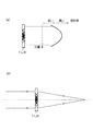
固定レンズ領域を形成する屈折率分布レンズは、平板形状のものを採用し、平板形状内部に屈折率の勾配をつけ、この屈折率の勾配によって光を曲げて結像作用を持たせたレンズである。より詳しくは、本実施形態で用いられる屈折率分布レンズは、光軸方向と垂直方向に屈折率勾配があるラジアル型屈折率分布レンズであり、両端面が平面でもレンズ作用が得られるようになっている。例えば、屈折率分布レンズの屈折率分布が、図2(a)に示すように、中心部の屈折率を最も高く、中心部から離れるに従って低くなるような場合は、図2(b)に示すように、屈折率分布レンズは凸レンズとして機能することになる。勿論、屈折率分布レンズの屈折率分布は、図2(a)に示すような屈折率分布に限定されるものではなく、他の屈折率分布、例えば、凹レンズとして機能するような屈折率分布など、としてもよい。 The refractive index distribution lens that forms the fixed lens region is a flat lens with a refractive index gradient inside the flat plate shape, and the light is bent by this refractive index gradient to provide an imaging function. is there. More specifically, the refractive index distribution lens used in the present embodiment is a radial type refractive index distribution lens having a refractive index gradient in a direction perpendicular to the optical axis direction, and a lens action can be obtained even if both end surfaces are flat. ing. For example, when the refractive index distribution of the refractive index distribution lens is such that the refractive index at the center is the highest as shown in FIG. 2A and becomes lower as the distance from the center increases, it is shown in FIG. Thus, the gradient index lens functions as a convex lens. Of course, the refractive index distribution of the refractive index distribution lens is not limited to the refractive index distribution as shown in FIG. 2A, but other refractive index distributions such as a refractive index distribution that functions as a concave lens. It is good also as.
また、液晶レンズ1は、図3(a)に示すように、2つの基板層の双方が固定レンズ領域を具備する構成としたが、本発明の液晶レンズはこのような構成に限定されるものではなく、図3(b)及び図3(c)に示すように、2つの基板層のいずれか一方が固定レンズ領域を具備する構成としてもよい。すなわち、液晶レンズ2は、均質なガラス基板41を有する第1基板層40、可変レンズ領域として機能する液晶層20、及び固定レンズ領域として機能する第2基板層30を備える構成である。また、液晶レンズ3は、固定レンズ領域として機能する第1基板層10、可変レンズ領域として機能する液晶層20、及び均質なガラス基板51を有する第2基板層50を備える構成である。
Further, as shown in FIG. 3A, the
尚、上述した固定レンズ領域は、平板状に形成されるのであれば、屈折率分布レンズに限定されないものであり、他のレンズ、例えば、回折レンズであってもよい。回折レンズは、光の回折現象を使って光を曲げて結像作用を持たせたレンズである。ここで、回折レンズの基板表面には微細パターンが記録されているため、第1基板11及び第2基板31の、液晶層20と接する面とは反対側の面(例えば、図1(b)に示す構成の液晶レンズ1において、第1基板11の左側面、第2基板31の右側面)は、厳密には平板形状ではないが、可視光の波長程度の溝は、巨視的に見て平板形状であるといってよい。すなわち、本明細書上で定義される「平板形状」は、固定レンズ領域の表面に生じた微細な凹凸も含む意であり、具体的には、固定レンズ領域の表面上に、最大、可視光の波長の10倍程度の溝が設けられた場合までを「平板形状」として許容する。このように、回折レンズの回折面は、液晶層と接する面とは反対側の面に設けられている。勿論、回折レンズは、基板表面に記録された微細パターンにより光学的レンズ作用が変わるため、屈折率分布レンズの場合と同様に、回折レンズを凸レンズ又は凹レンズとして機能させることが可能である。
The fixed lens region described above is not limited to a gradient index lens as long as it is formed in a flat plate shape, and may be another lens, for example, a diffractive lens. A diffractive lens is a lens that has an imaging function by bending light using a diffraction phenomenon of light. Here, since a fine pattern is recorded on the substrate surface of the diffractive lens, the surface of the
液晶層20は、電極12と電極32との間に印加された駆動電圧に応じて屈折率が変動する光学素子であり、外部電圧によって、レンズの焦点距離を任意に変えることが可能となっている。
The
以上のような構成の液晶レンズ1は、上述したように平板形状の固定レンズ領域を備えるため、従来からの量産生産方式を流用し、例えば、図4に示すような生産方法で作製することが出来る。すなわち、大きなガラス基板に上述した各層(配向膜、電極、液晶層)を形成させた後、各レンズのサイズに切り分けることで、液晶レンズ1を作成することができるので、一度に多くの液晶レンズ1を生産することができる。尚、第1基板11及び第2基板31を構成する屈折率分布レンズに関しては、例えば、イオン交換法を用いれば、図4に示すように、大きなガラス基板上にマトリックス状に集積配置された屈折率分布レンズを作成することができる。
As described above, the
図5は、液晶レンズ1の液晶層20の光学的レンズ作用を示す図である。詳しくは、図5(a)は、液晶層20に電圧を印可すると、液晶レンズ1の液晶層20が凸レンズの作用を奏する場合、図5(b)は、液晶層20に電圧を印可すると、液晶レンズ1の液晶層20が凹レンズの作用を奏する場合、図5(c)は、液晶層20に電圧を印可すると、液晶レンズ1の液晶層20が凸レンズと凹レンズの両方の作用を奏する場合を示している。
FIG. 5 is a diagram illustrating the optical lens action of the
上述したように、電極12と電極32の配置される位置及び電極の形状により、液晶レンズ1の液晶層20の光学的レンズ作用は変化するので、以下においては、電極12と電極32の配置される位置及び電極の形状を特定した実施例を用いて、液晶レンズ1(2,3)を具体的に説明する。ここで、図6乃至9は、各実施例の液晶レンズの断面図、左側面図及び右側面図である。尚、実施例1、2、11及び12は、液晶層20が凸レンズとして作用する場合、実施例3、4、5、6、13、14、15及び16は、液晶層20が凹レンズとして作用する場合、実施例7、8、9、10、17、18、19及び20は、液晶層20が凸レンズと凹レンズの両方の作用をする場合である。
As described above, the optical lens action of the
(実施例1)
実施例で記載している液晶とは、誘電率の符号が正の液晶を言うこととする。
Example 1
The liquid crystal described in the examples refers to a liquid crystal having a positive dielectric constant sign.
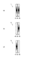
実施例1の液晶レンズ1Aは、固定レンズ領域である第1基板11及び第2基板31を備え、第1基板11及び第2基板31は、それぞれ屈折率分布レンズ(以下、各実施例では、屈折率分布レンズを11a、31aと表記し、回折レンズを11b、31bと表記する)11a及び31aから構成されている。また、第1電極12は、屈折率分布レンズ11aの、液晶層20と接する面とは反対側の面(左側面)に設けられており、電極は当該面の中央部に円形の孔を有する形状となっている。一方、第2電極32は、屈折率分布レンズ31aの、液晶層20と接する面(左側面)全体に渡って設けられている。
The
このような電極配置及び電極形状においては、特開2004−4616号公報に開示されるように、液晶層が凸レンズとして作用することが知られているので、液晶レンズ1Aは、可変レンズ領域の凸レンズとしての光学的レンズ作用と、固定レンズ領域の光学的レンズ作用と、を有することができる。これにより、液晶レンズ1Aは、従来の可変レンズ領域しか有しない液晶レンズよりも短焦点距離化を実現することができる。
In such an electrode arrangement and electrode shape, as disclosed in Japanese Patent Application Laid-Open No. 2004-4616, it is known that the liquid crystal layer acts as a convex lens. Therefore, the
尚、実施例1では、2つの固定レンズ領域を備えるようにしたが、これとは別に、1つの固定レンズ領域を備える液晶レンズとしてもよい。すなわち、屈折率分布レンズ11aを含む第1基板層10と、ガラス基板51を含む第2基板層50を備える液晶レンズ3Aとしてもよいし、ガラス基板41を含む第1基板層40と、屈折率分布レンズ31を含む第2基板層30を備える液晶レンズ2Aとしてもよい。
In the first embodiment, two fixed lens regions are provided. Alternatively, a liquid crystal lens having one fixed lens region may be used. That is, the liquid crystal lens 3A may include the
(実施例2)
実施例2の液晶レンズ2Bは、実施例1と電極配置及び電極形状は同一であるが、液晶レンズ1Aの屈折率分布レンズ11aをガラス基板41に、屈折率分布レンズ31aを回折レンズ31bに代えている。この場合、回折レンズ31bは屈折率分布レンズ31aと同一の光学的レンズ作用を奏するので、実施例1と同じ効果、すなわち、従来の可変レンズ領域しか有しない液晶レンズよりも短焦点距離化を実現することができる。
(Example 2)
The
尚、実施例2では、第2基板層が固定レンズ領域を具備する構成としたが、これとは別に第1基板層が固定レンズ領域を具備する構成としてもよいし、また、第1基板層及び第2基板層の双方が固定レンズ領域を具備する構成としてもよい。すなわち、回折レンズ11bを含む第1基板層10と、ガラス基板51を含む第2基板層50と、を備える液晶レンズ3Bとしてもよいし、回折レンズ11bを含む第1基板層10と、回折レンズ31bを含む第2基板層30と、を備えた液晶レンズ1Bとしてもよい。
In the second embodiment, the second substrate layer has a fixed lens region. Alternatively, the first substrate layer may have a fixed lens region, or the first substrate layer. The second substrate layer may have a fixed lens region. That is, a liquid crystal lens 3B including the
(実施例3)
実施例3の液晶レンズ1Cは、固定レンズ領域である第1基板11及び第2基板31を備え、第1基板11及び第2基板31は、それぞれ屈折率分布レンズ11a及び31aから構成されている。また、第1電極12は、屈折率分布レンズ11aの、液晶層20と接する面とは反対側の面(左側面)の中央部に円形に設けられている。一方、第2電極32は、屈折率分布レンズ31aの、液晶層20と接する面(左側面)全体に設けられている。
(Example 3)
The liquid crystal lens 1C of Example 3 includes a
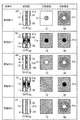
このような電極配置及び電極形状を備える液晶レンズ(可変レンズ領域のみ有する液晶レンズ)の電位分布を図10に示す。ここで、図10(a)は、液晶レンズの断面図、図10(b)は、液晶レンズの電位分布図である。より詳しくは、図10(b)は、第1電極12に5[V]の電圧を印加し、第2電極32に0[V]の電圧を印加した場合の断面における電位分布図である。図10(b)に示すように、電位分布曲線は、凹レンズの如き態様で分布しており、この電位に沿って液晶が配向するため、図10(a)に示す液晶レンズは凹レンズとして機能する。以上から、液晶レンズ1Cは、可変レンズ領域の凹レンズとしての光学的レンズ作用と、固定レンズ領域の光学的レンズ作用と、を有することができる。これにより、液晶レンズ1Cは、従来の可変レンズ領域しか有しない液晶レンズよりも短焦点距離化を実現することができる。
FIG. 10 shows a potential distribution of a liquid crystal lens (liquid crystal lens having only a variable lens region) having such an electrode arrangement and electrode shape. Here, FIG. 10A is a cross-sectional view of the liquid crystal lens, and FIG. 10B is a potential distribution diagram of the liquid crystal lens. More specifically, FIG. 10B is a potential distribution diagram in a cross section when a voltage of 5 [V] is applied to the
尚、実施例3では、2つの固定レンズ領域を備えるようにしたが、これとは別に、1つの固定レンズ領域を備える液晶レンズとしてもよい。すなわち、屈折率分布レンズ11aを含む第1基板層10と、ガラス基板51を含む第2基板層50を備える液晶レンズ3Cとしてもよいし、ガラス基板41を含む第1基板層40と、屈折率分布レンズ31aを含む第2基板層30を備える液晶レンズ2Cとしてもよい。
In the third embodiment, two fixed lens regions are provided. Alternatively, a liquid crystal lens having one fixed lens region may be used. In other words, the liquid crystal lens 3C may include the
(実施例4)
実施例4の液晶レンズ2Dは、実施例3と電極配置及び電極形状は同一であるが、液晶レンズ1Cの屈折率分布レンズ11aをガラス基板41に、屈折率分布レンズ31aを回折レンズ31bに代えている。すなわち、固定レンズ領域に回折レンズを用いた液晶レンズである。この場合、回折レンズ31bは屈折率分布レンズ31aと同一の光学的レンズ作用を奏するので、実施例3と同じ効果、すなわち、従来の可変レンズ領域しか有しない液晶レンズよりも短焦点距離化を実現することができる。
Example 4
The
尚、実施例4では、第2基板層が固定レンズ領域を具備する構成としたが、これとは別に第1基板層が固定レンズ領域を具備する構成としてもよいし、また、第1基板層及び第2基板層の双方が固定レンズ領域を具備する構成としてもよい。すなわち、回折レンズ11bを含む第1基板層10と、ガラス基板51を含む第2基板層50と、を備える液晶レンズ3Dとしてもよいし、回折レンズ11bを含む第1基板層10と、回折レンズ31bを含む第2基板層30と、を備えた液晶レンズ1Dとしてもよい。
In the fourth embodiment, the second substrate layer has a fixed lens region. Alternatively, the first substrate layer may have a fixed lens region, or the first substrate layer. The second substrate layer may have a fixed lens region. That is, the liquid crystal lens 3D may include the
(実施例5)
実施例5の液晶レンズ1Eは、固定レンズ領域である第1基板11及び第2基板31を備え、第1基板11及び第2基板31は、それぞれ屈折率分布レンズ11a及び31aから構成されている。また、第1電極12は、屈折率分布レンズ11aの、液晶層20と接する面とは反対側の面(左側面)の中央部に円形に設けられている。一方、第2電極32は、屈折率分布レンズ31aの、液晶層20と接する面に設けられており、電極は当該面の中央部に円形の孔を有する形状となっている。
(Example 5)
The
このような電極配置及び電極形状を備える液晶レンズ(可変レンズ領域のみ有する液晶レンズ)の電位分布を図11に示す。ここで、図11(a)は、液晶レンズの断面図、図11(b)は、液晶レンズの電位分布図である。より詳しくは、図11(b)は、第1電極12に5[V]の電圧を印加し、第2電極32に0[V]の電圧を印加した場合の断面における電位分布図である。図11(b)に示すように、電位分布曲線は、凹レンズの如き態様で分布しており、この電位に沿って液晶が配向するため、図11(a)に示す液晶レンズは凹レンズとして機能する。また、液晶層での電位勾配が、図10に示した液晶層での電位勾配と比較して、相対的に大きくなっているので、凹レンズ状に分布する傾向は図10に示す液晶レンズより強いことがわかる。従って、液晶レンズ1Eは、可変レンズ領域の凹レンズとしての光学的レンズ作用と、固定レンズ領域の光学的レンズ作用と、を有することができる。これにより、液晶レンズ1Eは、従来の可変レンズ領域しか有しない液晶レンズよりも短焦点距離化を実現することができる。また、液晶レンズ1Eは、液晶レンズ1Cよりも可変レンズ領域をより好適に凹レンズとして作用させることができる。
FIG. 11 shows a potential distribution of a liquid crystal lens (liquid crystal lens having only a variable lens region) having such an electrode arrangement and electrode shape. Here, FIG. 11A is a cross-sectional view of the liquid crystal lens, and FIG. 11B is a potential distribution diagram of the liquid crystal lens. More specifically, FIG. 11B is a potential distribution diagram in a cross section when a voltage of 5 [V] is applied to the
尚、実施例5では、2つの固定レンズ領域を備えるようにしたが、これとは別に、1つの固定レンズ領域を備える液晶レンズとしてもよい。すなわち、屈折率分布レンズ11aを含む第1基板層10とガラス基板51を含む第2基板層50を備える液晶レンズ3Eとしてもよいし、ガラス基板41を含む第1基板層40と屈折率分布レンズ31を含む第2基板層30を備える液晶レンズ2Eとしてもよい。
In the fifth embodiment, two fixed lens regions are provided. Alternatively, a liquid crystal lens having one fixed lens region may be used. That is, the liquid crystal lens 3E may include the
(実施例6)
実施例6の液晶レンズ2Fは、実施例5と電極配置及び電極形状は同一であるが、液晶レンズ1Eの屈折率分布レンズ11aをガラス基板41に、屈折率分布レンズ31aを回折レンズ31bに代えている。すなわち、固定レンズ領域に回折レンズを用いた液晶レンズである。この場合、回折レンズ31bは屈折率分布レンズ31aと同一の光学的レンズ作用を奏するので、実施例5と同じ効果、すなわち、従来の可変レンズ領域しか有しない液晶レンズよりも短焦点距離化を実現することができる。
(Example 6)
The
尚、実施例6では、第2基板層が固定レンズ領域を具備する構成としたが、これとは別に第1基板層が固定レンズ領域を具備する構成としてもよいし、また、第1基板層及び第2基板層の双方が固定レンズ領域を具備する構成としてもよい。すなわち、回折レンズ11bを含む第1基板層10と、ガラス基板51を含む第2基板層50と、を備える液晶レンズ3Fとしてもよいし、回折レンズ11bを含む第1基板層10と、回折レンズ31bを含む第2基板層30と、を備えた液晶レンズ1Fとしてもよい。
In the sixth embodiment, the second substrate layer has a fixed lens region. Alternatively, the first substrate layer may have a fixed lens region, or the first substrate layer. The second substrate layer may have a fixed lens region. In other words, the liquid crystal lens 3F may include the
(実施例7)
実施例7の液晶レンズ1Gは、固定レンズ領域である第1基板11及び第2基板31を備え、第1基板11及び第2基板31は、それぞれ屈折率分布レンズ11a及び31aから構成されている。また、第1電極12は、屈折率分布レンズ11aの、液晶層20と接する面(右側面)に設けられており、電極は当該面の中央部に円形の孔を有する形状となっている。一方、第2電極32は、屈折率分布レンズ31の、液晶層20と接する面(左側面)に設けられており、電極は当該面の中央部に円形の孔を有する形状となっている。
(Example 7)
The liquid crystal lens 1G of Example 7 includes a
このような電極配置及び電極形状は、「Jpn.J.Appl.Phys,2001,Vol.40,P.6514−6521」に開示されるように、液晶層が凸レンズ及び凹レンズの双方として作用することが知られているので、液晶レンズ1Gは、可変レンズ領域の凸レンズ及び凹レンズとしての光学的レンズ作用と、固定レンズ領域の光学的レンズ作用と、を有することができる。これにより、液晶レンズ1Gは、従来の可変レンズ領域しか有しない液晶レンズよりも短焦点距離化を実現することができる。 Such an electrode arrangement and electrode shape are such that the liquid crystal layer acts as both a convex lens and a concave lens as disclosed in “Jpn. J. Appl. Phys, 2001, Vol. 40, P. 6514-6521”. Therefore, the liquid crystal lens 1G can have an optical lens action as a convex lens and a concave lens in the variable lens area and an optical lens action in the fixed lens area. Thereby, the liquid crystal lens 1G can realize a shorter focal length than a liquid crystal lens having only a conventional variable lens region.
尚、実施例7では、2つの固定レンズ領域を備えるようにしたが、これとは別に、1つの固定レンズ領域を備える液晶レンズとしてもよい。すなわち、屈折率分布レンズ11aを含む第1基板層10とガラス基板51を含む第2基板層50を備える液晶レンズ3Gとしてもよいし、ガラス基板41を含む第1基板層40と屈折率分布レンズ31aを含む第2基板層30を備える液晶レンズ2Gとしてもよい。
In the seventh embodiment, two fixed lens regions are provided. Alternatively, a liquid crystal lens having one fixed lens region may be used. That is, the liquid crystal lens 3G may include the
(実施例8)
実施例8の液晶レンズ2Hは、実施例7と電極配置及び電極形状は同一であるが、液晶レンズ1Gの屈折率分布レンズ11aをガラス基板41に、屈折率分布レンズ31aを回折レンズ31bに代えている。この場合、回折レンズ31bは屈折率分布レンズ31aと同一の光学的レンズ作用を奏するので、実施例7と同じ効果、すなわち、従来の可変レンズ領域しか有しない液晶レンズよりも短焦点距離化を実現することができる。
(Example 8)
The
尚、実施例8では、第2基板層が固定レンズ領域を具備する構成としたが、これとは別に第1基板層が固定レンズ領域を具備する構成としてもよいし、また、第1基板層及び第2基板層の双方が固定レンズ領域を具備する構成としてもよい。すなわち、回折レンズ11bを含む第1基板層10と、ガラス基板51を含む第2基板層50と、を備える液晶レンズ3Hとしてもよいし、回折レンズ11bを含む第1基板層10と、回折レンズ31bを含む第2基板層30と、を備えた液晶レンズ1Hとしてもよい。
In Example 8, the second substrate layer has a fixed lens region. However, the first substrate layer may have a fixed lens region. Alternatively, the first substrate layer may have a fixed lens region. The second substrate layer may have a fixed lens region. In other words, the liquid crystal lens 3H may include the
(実施例9)
実施例9の液晶レンズ1Iは、固定レンズ領域である第1基板11及び第2基板31を備え、第1基板11及び第2基板31は、それぞれ屈折率分布レンズ11a及び31aから構成されている。また、第1電極12は、屈折率分布レンズ11aの、液晶層20と接する面(右側面)上全体に設けられている。一方、第2電極32は、屈折率分布レンズ31aの、液晶層20と接する面(左側面)に設けられており、電極は当該面の中央部に円形の孔を有する形状となっている。
Example 9
The liquid crystal lens 1I of Example 9 includes a
上述したように、実施例7に示す電極配置及び電極形状の液晶レンズの液晶層は、凸レンズ及び凹レンズの双方として作用することから、本実施例に示す電極配置及び電極形状の液晶レンズの液晶層も、同様にして、液晶層が凸レンズ及び凹レンズの双方として作用する。従って、液晶レンズ1Iは、可変レンズ領域の凸レンズ及び凹レンズとしての光学的レンズ作用と、固定レンズ領域の光学的レンズ作用と、を有することができる。これにより、液晶レンズ1Iは、従来の可変レンズ領域しか有しない液晶レンズよりも短焦点距離化を実現することができる。 As described above, since the liquid crystal layer of the electrode arrangement and the electrode-shaped liquid crystal lens shown in Example 7 functions as both a convex lens and a concave lens, the liquid crystal layer of the electrode arrangement and the electrode-shaped liquid crystal lens shown in this example. Similarly, the liquid crystal layer acts as both a convex lens and a concave lens. Accordingly, the liquid crystal lens 1I can have an optical lens action as a convex lens and a concave lens in the variable lens area, and an optical lens action in the fixed lens area. Thereby, the liquid crystal lens 1I can realize a shorter focal length than a liquid crystal lens having only a conventional variable lens region.
尚、実施例9では、2つの固定レンズ領域を備えるようにしたが、これとは別に、1つの固定レンズ領域を備える液晶レンズとしてもよい。すなわち、屈折率分布レンズ11aを含む第1基板層10とガラス基板51を含む第2基板層50を備える液晶レンズ2Iとしてもよいし、ガラス基板41を含む第1基板層40と屈折率分布レンズ31を含む第2基板層30を備える液晶レンズ3Iとしてもよい。
In the ninth embodiment, two fixed lens regions are provided. Alternatively, a liquid crystal lens including one fixed lens region may be used. That is, the liquid crystal lens 2I may include the
(実施例10)
実施例10の液晶レンズ2Jは、実施例9と電極配置及び電極形状は同一であるが、液晶レンズ1Iの屈折率分布レンズ11aを均質ガラス基板41に、屈折率分布レンズ31aを回折レンズ31bに代えている。この場合、回折レンズ31bは屈折率分布レンズ11aと同一の光学的レンズ作用を奏するので、実施例9と同じ効果、すなわち、従来の可変レンズ領域しか有しない液晶レンズよりも短焦点距離化を実現することができる。
(Example 10)
The
尚、実施例10では、第2基板層が固定レンズ領域を具備する構成としたが、これとは別に第1基板層が固定レンズ領域を具備する構成としてもよいし、また、第1基板層及び第2基板層の双方が固定レンズ領域を具備する構成としてもよい。すなわち、回折レンズ11bを含む第1基板層10と、ガラス基板51を含む第2基板層50と、を備える液晶レンズ3Jとしてもよいし、回折レンズ11bを含む第1基板層10と、回折レンズ31bを含む第2基板層30と、を備えた液晶レンズ1Jとしてもよい。
In Example 10, the second substrate layer has a fixed lens region. Alternatively, the first substrate layer may have a fixed lens region, or the first substrate layer. The second substrate layer may have a fixed lens region. In other words, the liquid crystal lens 3J may include the
(実施例11〜20)
実施例11乃至20は、上述した実施例1乃至10を変形した実施例となっている(実施例1と実施例11、実施例2と実施例12、…、実施例10と実施例20が対応している)。具体的には、実施例11乃至16は、それぞれ実施例1乃至6の第2電極32を、屈折率分布レンズ31a(または回折レンズ31b)の、液晶層20と接する面(左側面)から、液晶層20と接する面とは反対側の面(右側面)に移動させたものである。また、実施例17乃至20は、それぞれ実施例7乃至10の第1電極12を、屈折率分布レンズ11a(またはガラス基板41)の、液晶層20と接する面(右側面)から、液晶層20と接する面とは反対側の面(左側面)に移動させるとともに、第2電極32を、屈折率分布レンズ31a(または回折レンズ31b)の、液晶層20と接する面(左側面)から、液晶層20と接する面とは反対側の面に移動させたものである。
(Examples 11 to 20)
Examples 11 to 20 are examples obtained by modifying Examples 1 to 10 described above (Examples 1 and 11, Example 2 and Example 12, ..., Example 10 and Example 20). Yes) Specifically, in Examples 11 to 16, the
このように実施例11乃至20の液晶レンズは、実施例1乃至10の液晶レンズと電極の形状は同一であって、電極間の距離が離れただけなので、実施例11乃至20の液晶レンズの両電極間の電位分布曲線の態様は、実施例1乃至10の液晶レンズの電位分布曲線とほぼ同一となる。従って、実施例11乃至20は、それぞれ実施例1乃至10と同一の効果を有することができる。 As described above, the liquid crystal lenses of Examples 11 to 20 have the same shape as the liquid crystal lenses of Examples 1 to 10 and the distance between the electrodes is long, so that the liquid crystal lenses of Examples 11 to 20 are the same. The mode of the potential distribution curve between both electrodes is substantially the same as the potential distribution curve of the liquid crystal lenses of Examples 1 to 10. Therefore, Examples 11 to 20 can have the same effects as Examples 1 to 10, respectively.
以上、実施例1から実施例20に係る液晶レンズについて説明したが、本発明の液晶レンズは、上記実施例に限定されるものでなく、電極12と電極32の配置される位置及び電極の形状には他のバリエーションも含まれるのは勿論である。例えば、電極の形状及び電極に設けられた孔は、上記実施例では、円形としたが、この他、楕円形や多角形であってもよいものである。また、固定レンズ領域に屈折率分布レンズと回折レンズをそれぞれ用いた構成としてもよい。例えば、屈折率分布レンズ11aを含む第1基板層10と、回折レンズ31bを含む第2基板層30を備える液晶レンズとしてもよい。
As described above, the liquid crystal lenses according to Examples 1 to 20 have been described. However, the liquid crystal lens of the present invention is not limited to the above examples, and the positions where the
以上説明したように、本実施形態の液晶レンズは、第1電極12を備える平板形状の第1基板と、第1基板と対向し、第2電極32を備える平板形状の第2基板と、第1基板と第2基板に挟まれ、第1の電極と第2の電極との間に加えられる電圧に応じて屈折率が変化する液晶層20と、を有し、第1基板及び第2基板の少なくともいずれか一方は、平板形状のレンズであるので、量産性に優れるとともに、短焦点距離化を実現することができる。
As described above, the liquid crystal lens of the present embodiment includes a flat plate-shaped first substrate including the
1,2,3,1A〜1J,2A〜2J,3A〜3J 液晶レンズ
10,40 第1基板層
20 液晶層
11 第1基板
31 第2基板
12 第1電極
13,33 配向膜
30,50 第2基板層
32 第2電極
41,51 ガラス基板
1, 2, 3, 1A to 1J, 2A to 2J, 3A to 3J
Claims (4)
前記第1の基板と対向し、第2の電極を備える第2の平板形状の基板と、
前記第1の平板形状の基板と前記第2の平板形状の基板に挟まれ、前記第1の電極と前記第2の電極との間に加えられる電圧に応じて屈折率が変化する液晶層と、
を有し、前記第1の平板形状の基板及び前記第2の平板形状の基板の少なくともいずれか一方は、平板形状のレンズであることを特徴とする液晶レンズ。 A first plate-shaped substrate comprising a first electrode;
A second flat-plate-shaped substrate facing the first substrate and provided with a second electrode;
A liquid crystal layer sandwiched between the first plate-shaped substrate and the second plate-shaped substrate, the refractive index of which varies according to the voltage applied between the first electrode and the second electrode; ,
A liquid crystal lens, wherein at least one of the first flat plate-shaped substrate and the second flat plate-shaped substrate is a flat plate-shaped lens.
Priority Applications (1)
| Application Number | Priority Date | Filing Date | Title |
|---|---|---|---|
| JP2005302351A JP2007114231A (en) | 2005-10-17 | 2005-10-17 | Liquid crystal lens |
Applications Claiming Priority (1)
| Application Number | Priority Date | Filing Date | Title |
|---|---|---|---|
| JP2005302351A JP2007114231A (en) | 2005-10-17 | 2005-10-17 | Liquid crystal lens |
Publications (2)
| Publication Number | Publication Date |
|---|---|
| JP2007114231A true JP2007114231A (en) | 2007-05-10 |
| JP2007114231A5 JP2007114231A5 (en) | 2008-10-30 |
Family
ID=38096528
Family Applications (1)
| Application Number | Title | Priority Date | Filing Date |
|---|---|---|---|
| JP2005302351A Pending JP2007114231A (en) | 2005-10-17 | 2005-10-17 | Liquid crystal lens |
Country Status (1)
| Country | Link |
|---|---|
| JP (1) | JP2007114231A (en) |
Cited By (2)
| Publication number | Priority date | Publication date | Assignee | Title |
|---|---|---|---|---|
| KR100818481B1 (en) | 2007-06-08 | 2008-04-02 | 삼성전기주식회사 | Liquid crystal lens with inner electrode pattern and method of manufacturing the same |
| JP2012068607A (en) * | 2010-09-24 | 2012-04-05 | Silicon Touch Technology Inc | Liquid crystal lens |
Citations (4)
| Publication number | Priority date | Publication date | Assignee | Title |
|---|---|---|---|---|
| JPH0653537A (en) * | 1992-07-31 | 1994-02-25 | Japan Energy Corp | Semiconductor light receiving element |
| JPH06308453A (en) * | 1993-04-27 | 1994-11-04 | Toyota Motor Corp | Liquid crystal optical element |
| JP2002514315A (en) * | 1997-01-29 | 2002-05-14 | コーニング インコーポレイテッド | LCD panel surface lens array and manufacturing method |
| JP2003057411A (en) * | 2001-08-20 | 2003-02-26 | Fusao Terada | Variable focus lens |
-
2005
- 2005-10-17 JP JP2005302351A patent/JP2007114231A/en active Pending
Patent Citations (4)
| Publication number | Priority date | Publication date | Assignee | Title |
|---|---|---|---|---|
| JPH0653537A (en) * | 1992-07-31 | 1994-02-25 | Japan Energy Corp | Semiconductor light receiving element |
| JPH06308453A (en) * | 1993-04-27 | 1994-11-04 | Toyota Motor Corp | Liquid crystal optical element |
| JP2002514315A (en) * | 1997-01-29 | 2002-05-14 | コーニング インコーポレイテッド | LCD panel surface lens array and manufacturing method |
| JP2003057411A (en) * | 2001-08-20 | 2003-02-26 | Fusao Terada | Variable focus lens |
Cited By (2)
| Publication number | Priority date | Publication date | Assignee | Title |
|---|---|---|---|---|
| KR100818481B1 (en) | 2007-06-08 | 2008-04-02 | 삼성전기주식회사 | Liquid crystal lens with inner electrode pattern and method of manufacturing the same |
| JP2012068607A (en) * | 2010-09-24 | 2012-04-05 | Silicon Touch Technology Inc | Liquid crystal lens |
Similar Documents
| Publication | Publication Date | Title |
|---|---|---|
| US9122112B2 (en) | Liquid crystal lens, controlling method thereof and 3D display using the same | |
| JP5486465B2 (en) | Double layer liquid crystal lens device | |
| US8493658B2 (en) | Polarizer and display device including polarizer | |
| US10353238B2 (en) | Liquid crystal lens and 3D display device | |
| US10551716B2 (en) | Lens device | |
| KR101377728B1 (en) | Curvature reduction for switchable liquid crystal lens array | |
| JP5334116B2 (en) | Low voltage liquid crystal lens | |
| JP2006313243A (en) | Liquid crystal lens | |
| JP2012141552A (en) | Liquid crystal cylindrical lens array and display device | |
| TWI495943B (en) | Liquid crystal panel, driving method thereof, and liquid crystal display containing the same | |
| JP2006313248A (en) | Liquid crystal lens | |
| TWI417574B (en) | Zoom lens array and switchable two and three dimensional display | |
| US20070040972A1 (en) | Flexible display device | |
| JP2010107686A (en) | Method for manufacturing liquid crystal lens, and liquid crystal lens | |
| JP2011099999A (en) | Liquid crystal optical device | |
| JP2020531909A (en) | Optical device with liquid crystal orientation | |
| JP2007114231A (en) | Liquid crystal lens | |
| JP5501142B2 (en) | Liquid crystal lens and driving method thereof | |
| US10824020B2 (en) | Polarization independent optical phase modulator | |
| US10613404B2 (en) | Liquid crystal optical element and optical apparatus | |
| JP2007310092A (en) | Actuating reflection/absorption plate, and display element using the same | |
| KR101866193B1 (en) | Bi-focal gradient index lens and method for fabricating the lens | |
| JP2009223301A (en) | Liquid crystal lens | |
| JP2009229963A (en) | Liquid crystal optical element | |
| JP2009210964A (en) | Liquid crystal optical element |
Legal Events
| Date | Code | Title | Description |
|---|---|---|---|
| A521 | Written amendment |
Free format text: JAPANESE INTERMEDIATE CODE: A523 Effective date: 20080916 |
|
| A621 | Written request for application examination |
Free format text: JAPANESE INTERMEDIATE CODE: A621 Effective date: 20080916 |
|
| A977 | Report on retrieval |
Free format text: JAPANESE INTERMEDIATE CODE: A971007 Effective date: 20110427 |
|
| A131 | Notification of reasons for refusal |
Free format text: JAPANESE INTERMEDIATE CODE: A131 Effective date: 20110502 |
|
| A02 | Decision of refusal |
Free format text: JAPANESE INTERMEDIATE CODE: A02 Effective date: 20110906 |