JP2007079848A - Power unit and electronic equipment using the same - Google Patents
Power unit and electronic equipment using the same Download PDFInfo
- Publication number
- JP2007079848A JP2007079848A JP2005265892A JP2005265892A JP2007079848A JP 2007079848 A JP2007079848 A JP 2007079848A JP 2005265892 A JP2005265892 A JP 2005265892A JP 2005265892 A JP2005265892 A JP 2005265892A JP 2007079848 A JP2007079848 A JP 2007079848A
- Authority
- JP
- Japan
- Prior art keywords
- power supply
- microprocessor
- voltage
- supply voltage
- system controller
- Prior art date
- Legal status (The legal status is an assumption and is not a legal conclusion. Google has not performed a legal analysis and makes no representation as to the accuracy of the status listed.)
- Pending
Links
Images


Classifications
-
- G—PHYSICS
- G06—COMPUTING; CALCULATING OR COUNTING
- G06F—ELECTRIC DIGITAL DATA PROCESSING
- G06F1/00—Details not covered by groups G06F3/00 - G06F13/00 and G06F21/00
- G06F1/26—Power supply means, e.g. regulation thereof
Abstract
Description
この発明は、CPUなどのマイクロプロセッサに対して電源電圧を供給する電源装置に関する。 The present invention relates to a power supply apparatus that supplies a power supply voltage to a microprocessor such as a CPU.
パーソナルコンピュータやワークステーション、あるいはゲーム機器などに使用されるCPUなどのマイクロプロセッサには、電圧レギュレータ回路(以下、単にレギュレータ回路ともいう)によって安定化された所定の電源電圧が供給される。マイクロプロセッサに供給すべき電源電圧は、マイクロプロセッサの半導体製造プロセスなどに応じて設定され、近年の低電圧プロセスを用いたマイクロプロセッサの電源電圧は1.2V程度となっている。 A predetermined power supply voltage stabilized by a voltage regulator circuit (hereinafter also simply referred to as a regulator circuit) is supplied to a microprocessor such as a CPU used in a personal computer, a workstation, or a game machine. The power supply voltage to be supplied to the microprocessor is set according to the semiconductor manufacturing process of the microprocessor, and the power supply voltage of the microprocessor using the low voltage process in recent years is about 1.2V.
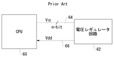
現在、複数のベンダーによって様々なマイクロプロセッサが供給されている。各ベンダーから供給されるマイクロプロセッサは、レギュレータ回路に対し、独自の方式によって自身に供給すべき電源電圧を指示している。言い換えれば、レギュレータ回路は、マイクロプロセッサからの電源電圧の指定を受け付けられるように設計される。図6は、従来のマイクロプロセッサとレギュレータ回路の構成例を示すブロック図である。 Currently, various microprocessors are supplied by a plurality of vendors. The microprocessor supplied from each vendor instructs the power supply voltage to be supplied to the regulator circuit by a unique method. In other words, the regulator circuit is designed to accept the designation of the power supply voltage from the microprocessor. FIG. 6 is a block diagram showing a configuration example of a conventional microprocessor and regulator circuit.
図6に示すように、マイクロプロセッサ60と、レギュレータ回路62間は、たとえば5ビットの信号線64でパラレル接続されている。マイクロプロセッサ60は、この信号線64を介してVID(Voltage ID)信号を送信し、レギュレータ回路62に対して自身に供給すべき電源電圧Vddを指示する。レギュレータ回路62は、マイクロプロセッサ60によって指示された電源電圧Vddを生成し、電源ライン66を介してマイクロプロセッサ60に供給する。このような構成をとることにより、たとえばマイクロプロセッサ60およびレギュレータ回路62が搭載される機器(以下単にセットともいう)の出荷後において、ユーザが別のマイクロプロセッサ60に交換した場合にも、交換後のマイクロプロセッサ60に最適な電源電圧Vddを供給することができる。
As shown in FIG. 6, the
しかしながら、従来の技術では、セットメーカは、使用するマイクロプロセッサ10のベンダーを選定するときに、そのベンダーから供給されるマイクロプロセッサ10に対応したレギュレータ回路12を選択する必要があり、設計の自由度に制約を受けていた。また、信号線64によりレギュレータ回路62に送信されるVID信号は、そのビット数によって電源電圧Vddの分解能が制限されるため、細かな電圧設定が行えないという問題がある。
However, in the conventional technique, when the set manufacturer selects the vendor of the
本発明はこうした課題に鑑みてなされたものであり、その目的は、マイクロプロセッサに供給すべき電源電圧を柔軟に設定可能な電源装置の提供にある。 The present invention has been made in view of these problems, and an object thereof is to provide a power supply apparatus capable of flexibly setting a power supply voltage to be supplied to a microprocessor.
本発明のある態様は、マイクロプロセッサに対して電源電圧を供給する電源装置に関する。この電源装置は、マイクロプロセッサから出力される電圧指示信号にもとづき、マイクロプロセッサに供給すべき電源電圧を設定し、設定した電源電圧に対応した電圧設定信号を出力するシステムコントローラと、システムコントローラから出力される電圧設定信号にもとづき、システムコントローラにおいて設定された電源電圧を生成し、マイクロプロセッサに供給するレギュレータ回路と、を備える。 One embodiment of the present invention relates to a power supply device that supplies a power supply voltage to a microprocessor. This power supply device sets a power supply voltage to be supplied to the microprocessor based on a voltage instruction signal output from the microprocessor, and outputs a voltage setting signal corresponding to the set power supply voltage, and is output from the system controller. And a regulator circuit that generates a power supply voltage set in the system controller based on the voltage setting signal to be supplied to the microprocessor.
この態様によれば、電源装置にシステムコントローラを設け、レギュレータ回路ではなく、システムコントローラにおいて、電源電圧の設定を行うことにより、さまざまな状況に応じて適切な電源電圧をマイクロプロセッサに供給することができる。 According to this aspect, the system controller is provided in the power supply apparatus, and the power supply voltage is set in the system controller, not in the regulator circuit, so that an appropriate power supply voltage can be supplied to the microprocessor according to various situations. it can.
なお、以上の構成要素の任意の組合せ、本発明の表現を、方法、装置、システム、などの間で変換したものもまた、本発明の態様として有効である。 It should be noted that any combination of the above-described components and a representation of the present invention converted between a method, an apparatus, a system, etc. are also effective as an aspect of the present invention.
本発明によれば、マイクロプロセッサに供給すべき電源電圧を柔軟に設定することができる。 According to the present invention, the power supply voltage to be supplied to the microprocessor can be set flexibly.
はじめに、本発明の実施の形態に係る電源装置の概要について説明する。この電源装置は、パーソナルコンピュータやゲーム機器などの電子機器に搭載され、マイクロプロセッサに対して電源電圧を供給する電源装置である。 First, an outline of a power supply device according to an embodiment of the present invention will be described. This power supply device is a power supply device that is mounted on an electronic device such as a personal computer or a game machine and supplies a power supply voltage to a microprocessor.
ある態様の電源装置は、マイクロプロセッサから出力される電圧指示信号にもとづき、マイクロプロセッサに供給すべき電源電圧を設定し、設定した電源電圧に対応した電圧設定信号を出力するシステムコントローラと、システムコントローラから出力される電圧設定信号にもとづき、システムコントローラにおいて設定された電源電圧を生成し、マイクロプロセッサに供給するレギュレータ回路と、を備える。 A power supply device according to an aspect includes a system controller that sets a power supply voltage to be supplied to a microprocessor based on a voltage instruction signal output from the microprocessor, and outputs a voltage setting signal corresponding to the set power supply voltage, and a system controller And a regulator circuit that generates a power supply voltage set in the system controller based on the voltage setting signal output from the power supply and supplies the power supply voltage to the microprocessor.
この態様によると、システムコントローラにおいて、電源電圧の設定を行うことにより、さまざまな状況に応じて適切な電源電圧をマイクロプロセッサに供給することをできる。 According to this aspect, by setting the power supply voltage in the system controller, an appropriate power supply voltage can be supplied to the microprocessor according to various situations.
システムコントローラは、電圧指示信号と、マイクロプロセッサに供給すべき電源電圧との関係を保持する電圧設定テーブルを備えてもよい。また、電圧設定テーブルは、その保持するデータが、更新可能に構成されてもよい。 The system controller may include a voltage setting table that holds the relationship between the voltage instruction signal and the power supply voltage to be supplied to the microprocessor. Further, the voltage setting table may be configured so that the data held therein can be updated.
システムコントローラは、マイクロプロセッサの状態を取得し、取得した状態を電源電圧の設定に反映させてもよい。
マイクロプロセッサの状態は、マイクロプロセッサの使用時間、温度、演算量(演算負荷)などである。これらをパラメータとすることにより、マイクロプロセッサのそのときどきの状態に応じて最適な電源電圧を設定することができる。
The system controller may acquire the state of the microprocessor and reflect the acquired state in the setting of the power supply voltage.
The state of the microprocessor includes the usage time of the microprocessor, temperature, calculation amount (calculation load), and the like. By using these as parameters, it is possible to set an optimum power supply voltage according to the current state of the microprocessor.
システムコントローラと、マイクロプロセッサとは、バスを介して接続されてもよい。バスとしては、SPI(Serial Peripheral Interface)バスやI2Cバスを好適に用いることができ、多くの情報を送受信することが可能となる。 The system controller and the microprocessor may be connected via a bus. As the bus, an SPI (Serial Peripheral Interface) bus or an I2C bus can be suitably used, and a large amount of information can be transmitted and received.
マイクロプロセッサは、バスを介して通信を行い、電源電圧を動的に設定してもよい。「動的に設定」とは、一度システムコントローラにおいて設定された電源電圧をマイクロプロセッサに対して固定的に供給し続けるのではなく、マイクロプロセッサや本電源装置が搭載される機器の状態に応じて、電源電圧を設定することをいう。 The microprocessor may communicate via the bus and dynamically set the power supply voltage. “Dynamically set” means that the power supply voltage once set in the system controller is not continuously supplied to the microprocessor in a fixed manner, but depending on the state of the device in which the microprocessor and the power supply device are mounted. This means setting the power supply voltage.
レギュレータ回路は、デジタル信号として入力される電圧設定信号にもとづいて、電源電圧を生成するものであり、システムコントローラとレギュレータ回路は、デジタル信号線を介して接続されてもよい。
この場合、従来のマイクロプロセッサへの電源供給へ用いられるレギュレータ回路を用いることができる。
The regulator circuit generates a power supply voltage based on a voltage setting signal input as a digital signal, and the system controller and the regulator circuit may be connected via a digital signal line.
In this case, a regulator circuit used for power supply to a conventional microprocessor can be used.
レギュレータ回路は、アナログ信号として入力される電圧設定信号にもとづいて、電源電圧を生成するものであり、システムコントローラから出力されるデジタルの電圧設定信号をアナログの電圧設定信号に変換して、レギュレータ回路に出力するデジタルアナログ変換器をさらに備えてもよい。
この場合、アナログ入力される電圧にもとづいて出力電圧を設定する汎用的なレギュレータ回路を用いることができる。
The regulator circuit generates a power supply voltage based on a voltage setting signal input as an analog signal. The regulator circuit converts the digital voltage setting signal output from the system controller into an analog voltage setting signal. A digital-to-analog converter that outputs the signal may be further provided.
In this case, a general-purpose regulator circuit that sets an output voltage based on an analog input voltage can be used.
マイクロプロセッサに供給される電源電圧をアナログデジタル変換するアナログデジタル変換器をさらに備えてもよい。システムコントローラは、アナログデジタル変換器の出力信号と、レギュレータ回路に出力する電圧設定信号から、マイクロプロセッサでの消費電力を算出する電力算出部を含んでもよい。 An analog-to-digital converter that performs analog-to-digital conversion on the power supply voltage supplied to the microprocessor may be further provided. The system controller may include a power calculation unit that calculates power consumption in the microprocessor from the output signal of the analog-digital converter and the voltage setting signal output to the regulator circuit.
システムコントローラにおいて設定したマイクロプロセッサに供給すべき電源電圧と、実際にマイクロプロセッサに供給される電圧を比較することにより、電源ラインのインピーダンスが既知である場合、マイクロプロセッサに流れる電流を計算することができる。 By comparing the power supply voltage to be supplied to the microprocessor set in the system controller with the voltage actually supplied to the microprocessor, the current flowing through the microprocessor can be calculated when the impedance of the power supply line is known. it can.
以下、本発明の実施の形態に係る電源装置の詳細を、図面を参照しつつ説明する。
(第1の実施の形態)
図1は、第1の実施の形態に係る電子機器1000の構成を示すブロック図である。電子機器1000は、CPUやグラフィックプロセッサなどのマイクロプロセッサ10と、マイクロプロセッサ10に対して電源電圧Vddを供給する電源装置100を含む。以降の図において、同一または同等の構成要素には同一の符号を付し、適宜説明を省略するものとする。電源装置100により駆動されるマイクロプロセッサ10は、典型的には1.2V程度の電源電圧で動作するものである。しかしながら、実際には、実行する演算処理の内容、マイクロプロセッサ10の温度、あるいは、実装されてからの使用年月などのさまざまな要因によって、最適な電源電圧Vddは変化する。以下、いくつかの実施の形態にもとづいて、マイクロプロセッサ10に最適な電源電圧Vddを供給する電源装置100について説明する。
Hereinafter, details of the power supply device according to the embodiment of the present invention will be described with reference to the drawings.
(First embodiment)
FIG. 1 is a block diagram illustrating a configuration of an
以下、第1の実施の形態に係る電源装置100の構成について説明する。電源装置100は、レギュレータ回路12およびシステムコントローラ20を含む。システムコントローラ20とマイクロプロセッサ10とは、第1信号線14を介して接続される。このシステムコントローラ20には、第1信号線14を介してマイクロプロセッサ10から出力される電圧指示信号Dcnfが入力される。システムコントローラ20は、この電圧指示信号Dcnfにもとづき、マイクロプロセッサ10が要求する最適な電源電圧Vddを設定する。後述するように、システムコントローラ20は、マイクロプロセッサ12の状態を取得し、取得した状態を電源電圧Vddの設定に反映させる。
Hereinafter, the configuration of the
システムコントローラ20とレギュレータ回路12は、nビットの第2信号線16により接続される。システムコントローラ20は、電圧指示信号Dcnfにもとづいて設定した最適な電源電圧を、nビットのデジタル電圧設定信号Dsetとしてレギュレータ回路12に出力する。
The
レギュレータ回路12は、nビットの入力端子44を備え、入力端子44に入力される信号に応じたアナログの電源電圧Vddを生成し、出力端子42から出力する。本実施の形態において使用するレギュレータ回路12は、図6に示す従来のレギュレータ回路62と同等の機能を有するものである。
The
レギュレータ回路12の入力端子44には、第2信号線16を介して電圧設定信号Dsetが入力されている。すなわち、レギュレータ回路12は、システムコントローラ20からの指示を受け、システムコントローラ20において設定された最適な電源電圧Vddを生成する。レギュレータ回路12の出力端子42から出力される電源電圧Vddは、電源ライン18を介してマイクロプロセッサ10に供給される。
The voltage setting signal Dset is input to the
図2は、システムコントローラ20の内部構成を示すブロック図である。システムコントローラ20は、インターフェース部22、電源電圧設定部24、電圧設定テーブル26を含む。インターフェース部22は、システムコントローラ20の外部に接続されるマイクロプロセッサ10およびレギュレータ回路12などのブロックと、電源電圧設定部24間の信号の送受信を制御する。たとえば、マイクロプロセッサ10とシステムコントローラ20を接続する第1信号線14は、SPIバスであってもよい。この場合、マイクロプロセッサ10とシステムコントローラ20は、データイン、データアウト、クロック、チップセレクトに対応した4本の信号線で接続される。マイクロプロセッサ10およびシステムコントローラ20間をSPIバスで接続した場合、インターフェース部22は、SPIに対応した信号処理を行い、電圧指示信号Dcnfを電源電圧設定部24に転送する。なお、SPIバスに代えて、I2Cバスなどを用いてもよい。
FIG. 2 is a block diagram showing an internal configuration of the
電源電圧設定部24には、マイクロプロセッサ10から出力されるデジタルの電圧指示信号Dcnfが入力されている。また、電源電圧設定部24は、電圧設定テーブル26と接続される。電圧設定テーブル26は、デジタルの電圧指示信号Dcnfと、マイクロプロセッサ10に供給すべき最適な電源電圧Vddとの関係を、本電源装置100を含む機器の状態をパラメータとして保持している。
The power supply
システムコントローラ20の電源電圧設定部24は、電圧指示信号Dcnfをもとに、電圧設定テーブル26を参照し、セットがおかれる状況に応じて最適な電源電圧Vddを設定する。以下に、システムコントローラ20における電圧指示信号Dcnfにもとづく電源電圧Vddの設定方法について説明する。
The power supply
(設定方法1)
たとえば、電圧設定テーブル26には、電圧指示信号Dcnfとマイクロプロセッサ10に供給すべき電源電圧Vddの関係が、本電源装置100が搭載されるセットの出荷後の経過時間τをパラメータとして記憶されている。
(Setting method 1)
For example, in the voltage setting table 26, the relationship between the voltage instruction signal Dcnf and the power supply voltage Vdd to be supplied to the
マイクロプロセッサ10は、ゲートと呼ばれる無数のトランジスタ素子が集積化されて構成される。このトランジスタ素子が安定に動作する電源電圧レベルは、経時劣化によって、徐々に上昇することが知られている。そこで、従来のマイクロプロセッサに対する電源供給技術では、このような経年劣化を踏まえて、初期状態において本来必要な電源電圧よりも高い電圧を供給する必要があった。このことは、マイクロプロセッサ10において余分な電力を消費していることを意味する。
The
一方、本実施の形態に係る電源装置100では、システムコントローラ20において、出荷後の経過時間τを管理し、経過時間に応じて、マイクロプロセッサ10に供給すべき電源電圧Vddの設定値を徐々に上昇させる。図3は、デジタルの電圧指示信号Dcnf、経過時間τ、および最適な電源電圧Vddの関係図であり、電圧設定テーブル26の内容を示す図である。
On the other hand, in the
マイクロプロセッサ10からは、品種ごと、ロットごと、あるいは個別のプロセッサごとに予め定められたデジタルの電圧指示信号Dcnfが出力される。システムコントローラ20は、セット出荷後の経過時間τと、電圧指示信号Dcnfにもとづき、電圧設定テーブル26を参照して、最適な電源電圧Vddを決定する。たとえば、あるマイクロプロセッサ10から電圧指示信号Dcnf1が出力されており、経過時間がτ1であった場合、最適な電源電圧はVdd1となる。電圧設定テーブル26には、最適な電源電圧Vddの値がnビットのデジタル値として記憶されており、電源電圧設定部24は、このデジタル値をデジタル電圧設定信号Dsetとしてレギュレータ回路12に出力する。
The
このように、本設定方法によれば、セットの出荷後の経過時間τに応じて、電源電圧Vddを調節することにより、必要以上に高い電源電圧を供給する必要がなくなるため、消費電力を低減することが可能となる。 Thus, according to this setting method, it is not necessary to supply a power supply voltage higher than necessary by adjusting the power supply voltage Vdd according to the elapsed time τ after shipment of the set, thereby reducing power consumption. It becomes possible to do.
なお、セット出荷後の経過時間τは、システムコントローラ20自身で管理して取得してもよいし、マイクロプロセッサ10において管理しておき、第1信号線14を介して取得してもよく、あるいは、外部の処理ブロックから取得してもよい。
また、システムコントローラ20は、出荷後の経過時間τに代えて、マイクロプロセッサ10の積算使用時間を管理して、電源電圧Vddを設定してもよい。
The elapsed time τ after set shipment may be managed and acquired by the
Further, the
(設定方法2)
設定方法2では、マイクロプロセッサ10の演算処理量(演算負荷)をモニタし、演算負荷に応じて電源電圧Vddを最適な値に設定する。マイクロプロセッサ10の演算負荷は、電圧指示信号Dcnfとともに、第1信号線14を介してマイクロプロセッサ10から入力される。上述のように、第1信号線14をSPIバスやI2Cバスとした場合には、このような付加的な情報の送受信が可能となる。
(Setting method 2)
In the setting method 2, the amount of calculation processing (calculation load) of the
この設定方法では、マイクロプロセッサ10から電源電圧設定部24に対して、電圧指示信号Dcnfおよび演算負荷を表す演算負荷信号SigLが出力される。電圧設定テーブル26には、演算負荷信号SigLおよび電圧指示信号Dcnfと、電源電圧Vddの関係が記憶される。電源電圧設定部24は、電圧設定テーブル26を参照して、現在の演算負荷信号SigLと、電圧指示信号Dcnfにもとづいて、設定電圧Dsetを決定し、レギュレータ回路12へと指示する。
In this setting method, the
この設定方法によれば、マイクロプロセッサ10の演算量や動作クロックに応じて、電源電圧Vddを好適に制御することができる。
According to this setting method, the power supply voltage Vdd can be suitably controlled according to the calculation amount of the
(設定方法3)
本設定方法では、システムコントローラ20は、マイクロプロセッサ10の温度THをモニタし、マイクロプロセッサ10の温度に応じてマイクロプロセッサ10に供給すべき電源電圧Vddを調節する。マイクロプロセッサ10の温度THは、たとえばサーミスタなどを用いた温度検出回路によって、電圧信号(以下、温度検出電圧Vthという)として取得することができる。温度検出電圧Vthは、インターフェース部22、あるいは外部のA/Dコンバータによりデジタル値に変換された後、電源電圧設定部24へと入力される。
(Setting method 3)
In this setting method, the
電圧設定テーブル26には、電圧指示信号Dcnfと電源電圧Vddの関係が、マイクロプロセッサ10の温度THをパラメータとして記憶されており、電源電圧設定部24は、電圧設定テーブル26を参照することにより、最適な電源電圧Vddをレギュレータ回路12に対して指示することができる。
The voltage setting table 26 stores the relationship between the voltage instruction signal Dcnf and the power supply voltage Vdd using the temperature TH of the
(設定方法4)
セットの低消費電力化の観点からみると、マイクロプロセッサ10に供給すべき電源電圧Vddは、マイクロプロセッサ10が動作可能な範囲で、なるべく低く設定することが望ましい。そこで、設定方法4では、電源電圧設定部24とマイクロプロセッサ10が双方向通信を行いながら、最適な電源電圧Vddを動的に設定する。
(Setting method 4)
From the viewpoint of reducing the power consumption of the set, it is desirable that the power supply voltage Vdd to be supplied to the
具体的には電源電圧設定部24とマイクロプロセッサ10は、以下の動作を行うことによって最適な電源電圧Vddを設定する。
まず、電源電圧設定部24は、初期電源電圧VddINITを設定する。この初期電源電圧VddINITは、マイクロプロセッサ10が確実に動作する値に設定することが望ましい。
電源電圧設定部24は、設定した初期電源電圧VddINITに対応する電圧設定信号Dsetをレギュレータ回路12に対して出力する。レギュレータ回路12は、入力された電圧設定信号Dsetにもとづいて、初期電源電圧VddINITを生成し、マイクロプロセッサ10へと出力する。
Specifically, the power supply
First, the power supply
The power supply
マイクロプロセッサ10は、初期電源電圧VddINITが印加された状態で安定に動作可能かどうかを表すイネーブル信号ENを、第1信号線14を介して電源電圧設定部24へと出力する。イネーブル信号ENはハイレベル(1)のとき動作可能、ローレベル(0)のとき動作不能を表すものとする。電源電圧設定部24は、イネーブル信号ENがハイレベルのとき、電圧設定信号Dsetを、電源電圧Vddが低下する方向にシフトし、レギュレータ回路12へと出力する。その結果、マイクロプロセッサ10には、初期電源電圧VddINITよりも低い電源電圧が供給される。
The
マイクロプロセッサ10は、現在の電源電圧Vddで安定に動作可能かを判定し、イネーブル信号ENを電源電圧設定部24へと送信する。このとき、電源電圧設定部24は、イネーブル信号ENがハイレベルであればさらに電源電圧Vddを低下させ、逆にローレベルであれば、電源電圧Vddを上昇させる。
The
本設定方法では、マイクロプロセッサ10とシステムコントローラ20が上記手順を繰り返すことによって、マイクロプロセッサ10が動作可能な最小の電源電圧Vddを設定することができる。さらに、この方式を用いる場合、電圧設定テーブル26は設けなくてもよい。
In this setting method, the minimum power supply voltage Vdd at which the
このように、本実施の形態に係る電源装置100によれば、レギュレータ回路12ではなく、システムコントローラ20において、電源電圧Vddの設定を行うため、セットがおかれる状況に応じて適切な電源電圧をマイクロプロセッサ10に供給することができる。
As described above, according to the
また、マイクロプロセッサ10とシステムコントローラ20間をSPIバスやI2Cバスで接続する場合、図6に示す従来の電源装置のように、マイクロプロセッサ10からnビットの信号線を出力する必要がないため、マイクロプロセッサ10のピン数を減らすことができる。
Further, when the
なお、設定方法1〜設定方法4で説明した設定方法は、単独で用いても良いし、任意で組み合わせてもよい。システムコントローラ20において、セット出荷後の経過時間τ、マイクロプロセッサ10の温度TH、あるいはマイクロプロセッサ10の演算負荷などの複数の要素を統合的に解析することにより、より最適な電源電圧Vddを設定することができる。
In addition, the setting method demonstrated by the setting method 1-the setting method 4 may be used independently, and may be combined arbitrarily. The
システムコントローラ20に設けられた電圧設定テーブル26は、アップデート可能に構成されていても良い。たとえば、本電源装置100が搭載されるセットがパーソナルコンピュータやゲーム機器などのネットワーク機能を備える場合、LAN(Local Area Network)などを介して、ネットワークに接続することにより、新たな設定テーブルのデータをダウンロードすることができる。システムコントローラ20は、ダウンロードしたデータをもとに、電圧設定テーブル26の内容を書き換える。電圧設定テーブル26を必要に応じて更新することによって、不具合の修正や、より適切な電源電圧の設定が可能となる。なお、電圧設定テーブル26の更新は、CD−ROMやフレキシブルディスクなどのメディアなどによって行ってもよい。
The voltage setting table 26 provided in the
(第2の実施の形態)
第1の実施の形態では、出力電圧の設定をデジタル信号によって行うタイプのレギュレータ回路12を用いた電源装置100について説明した。以下で説明する第2の実施の形態では、アナログ電圧によって出力電圧を設定可能なレギュレータ回路を用いた電源装置110について説明する。
(Second Embodiment)
In the first embodiment, the
図4は、第2の実施の形態に係る電源装置110の構成を示すブロック図である。電源装置110は、レギュレータ回路40、D/Aコンバータ30、システムコントローラ20を備える。システムコントローラ20の構成およびマイクロプロセッサ10との接続態様については、第1の実施の形態と同じであるため、説明を省略する。
FIG. 4 is a block diagram illustrating a configuration of the
システムコントローラ20から第2信号線16を介して出力されるnビットのデジタルの電圧設定信号Dsetは、D/Aコンバータ30へと入力される。D/Aコンバータ30は、電圧設定信号Dsetをデジタルアナログ変換し、アナログの電圧設定信号Vsetに変換する。D/Aコンバータ30から出力される電圧設定信号Vsetは、レギュレータ回路40の入力端子44に入力される。
An n-bit digital voltage setting signal Dset output from the
レギュレータ回路40は、入力端子44に入力された電圧設定信号Vsetに応じて、電源電圧Vddを生成し、電源ライン18を介してマイクロプロセッサ10へと出力する。
The
本実施の形態によれば、汎用的なレギュレータ回路を利用することができる。さらに、システムコントローラ20から出力されるデジタルの電圧設定信号Dsetのビット数を増やすことにより、レギュレータ回路の出力電圧、すなわちマイクロプロセッサ10に供給する電源電圧Vddを従来の電源装置に比べて、より細かく調節することができる。
According to this embodiment, a general-purpose regulator circuit can be used. Furthermore, by increasing the number of bits of the digital voltage setting signal Dset output from the
(第3の実施の形態)
図5は、第3の実施の形態に係る電源装置120の構成を示すブロック図である。本実施の形態に係る電源装置120は、マイクロプロセッサ10の消費電流、消費電力を算出する機能を備える。
(Third embodiment)
FIG. 5 is a block diagram illustrating a configuration of the
本実施の形態に係る電源装置120は、システムコントローラ20’、レギュレータ回路12、ローパスフィルタ50、A/Dコンバータ52を備える。
The
一般的なレギュレータ回路12は、制御対象の電圧、すなわち電源電圧Vddが、電圧設定信号Dsetによって指示される目標値に近づくように帰還制御を行っている。本実施の形態では、実際にマイクロプロセッサ10に印加されている電源電圧Vddが、帰還電圧Vfbとしてレギュレータ回路12に帰還されている。レギュレータ回路12は、帰還電圧Vfbが目標値に近づくように電圧生成を行う。
The
帰還電圧Vfbは、ローパスフィルタ50を介してA/Dコンバータ52へと入力される。帰還電圧Vfbは、高周波成分の除去によって平滑化された後、A/Dコンバータ52によってデジタルの帰還信号Dfbに変換される。帰還信号Dfbは、システムコントローラ20へと入力される。
The feedback voltage Vfb is input to the A /
本実施の形態に係るシステムコントローラ20’は、図2に加えて、電力算出部28を備える。電力算出部28には、電源電圧設定部24から出力される電圧設定信号DsetおよびA/Dコンバータ52から出力される帰還信号Dfbが入力されており、2つの信号にもとづき、マイクロプロセッサ10における消費電流および消費電力を算出する。
The
レギュレータ回路12によって生成した電源電圧Vddは、電源ライン18を介してマイクロプロセッサ10に印加される。ここで電源ライン18は、微小な抵抗成分RLを有しているため、負荷電流ILが流れることによって電圧降下ΔVが発生する。電圧降下ΔVと、抵抗成分RL、負荷電流ILの間には、IL=ΔV/RLの関係式が成り立つ。
The power supply voltage Vdd generated by the
本実施の形態において、電源ライン18での電圧降下ΔVは、ΔV=Vdd−Vfbによって求めることができる。ここで、Vddは、電圧設定信号Dsetにより指示された電圧値であり、Vfbは、実際にマイクロプロセッサ10に印加される電圧である。電力算出部28は、Vddに対応する電圧設定信号Dsetと、Vfbに対応する帰還信号Dfbによって、電圧降下ΔVを算出する。
In the present embodiment, the voltage drop ΔV in the
電源ライン18の抵抗成分RLは予め測定しておく。電力算出部28は、電圧設定信号Dsetおよび帰還信号Dfbから求めた電圧降下ΔVと、抵抗成分RLから上記関係式を用いて、マイクロプロセッサ10に流れる電流を算出する。
The resistance component RL of the
たとえば、電圧設定信号Dsetが1.2Vに対応した値を示しており、帰還信号Dfbが、1.08Vに対応した値を示しているとすると、電圧降下ΔV=0.l2Vとなる。また、電源ライン18の抵抗値がRL=1.2mΩであったとすると、マイクロプロセッサ10における消費電流ILは、IL=0.12V/1.2mΩ=100Aとなる。さらに消費電力は、P=I・V=100A×1.2V=120Wとなる。
For example, if the voltage setting signal Dset indicates a value corresponding to 1.2V and the feedback signal Dfb indicates a value corresponding to 1.08V, the voltage drop ΔV = 0. 12V. If the resistance value of the
電力算出部28はこのようにして算出したマイクロプロセッサ10の消費電流および消費電力を、外部に接続されるパフォーマンスモニタ54へと出力する。ユーザは、パフォーマンスモニタ54から、マイクロプロセッサ10の動作状態を知ることができる。
The
このように、本実施の形態に係る電源装置120によれば、システムコントローラ20’に、電力算出部28を設け、マイクロプロセッサ10の駆動経路上の一点の電圧を入力して電圧降下を測定することにより、マイクロプロセッサ10の消費電流あるいは消費電力を算出することができる。
As described above, according to the
さらに、本実施の形態に係る電源装置120において算出したマイクロプロセッサ10の消費電流あるいは消費電力を、第1の実施の形態で説明したように、マイクロプロセッサ10に供給する電源電圧Vddの設定に反映してもよい。
Further, the current consumption or power consumption of the
以上、本発明について、実施の形態をもとに説明した。この実施の形態は例示であり、それらの各構成要素や各処理プロセスの組合せにいろいろな変形例が可能なこと、またそうした変形例も本発明の範囲にあることは当業者に理解されるところである。 The present invention has been described based on the embodiments. This embodiment is an exemplification, and it will be understood by those skilled in the art that various modifications can be made to combinations of the respective constituent elements and processing processes, and such modifications are also within the scope of the present invention. is there.
実施の形態において、システムコントローラ20は、レギュレータ回路12を制御する処理を行ったが、このシステムコントローラ20に、その他の処理を実行させてもよい。たとえば、システムコントローラ20において、マイクロプロセッサ10の温度情報を取得する場合には、システムコントローラ20により、マイクロプロセッサ10を冷却するファンを制御してもよい。その他、システムコントローラ20をその他のブロックと接続することにより、統合的な処理を行うことができる。
In the embodiment, the
10 マイクロプロセッサ、 12 レギュレータ回路、 14 第1信号線、 16 第2信号線、 18 電源ライン、 20 システムコントローラ、 100 電源装置、 110 電源装置、 22 インターフェース部、 24 電源電圧設定部、 26 電圧設定テーブル、 28 電力算出部、 30 D/Aコンバータ、 40 レギュレータ回路、 50 ローパスフィルタ、 52 A/Dコンバータ、 54 パフォーマンスモニタ。
DESCRIPTION OF
Claims (13)
前記マイクロプロセッサから出力される電圧指示信号にもとづき、前記マイクロプロセッサに供給すべき電源電圧を設定し、設定した電源電圧に対応した電圧設定信号を出力するシステムコントローラと、
前記システムコントローラから出力される前記電圧設定信号にもとづき、前記システムコントローラにおいて設定された電源電圧を生成し、前記マイクロプロセッサに供給するレギュレータ回路と、
を備えることを特徴とする電源装置。 A power supply device for supplying a power supply voltage to a microprocessor,
A system controller that sets a power supply voltage to be supplied to the microprocessor based on a voltage instruction signal output from the microprocessor, and outputs a voltage setting signal corresponding to the set power supply voltage;
A regulator circuit that generates a power supply voltage set in the system controller based on the voltage setting signal output from the system controller and supplies the power supply voltage to the microprocessor;
A power supply apparatus comprising:
前記電圧指示信号と、前記マイクロプロセッサに供給すべき電源電圧との関係を保持する電圧設定テーブルを備えることを特徴とする請求項1に記載の電源装置。 The system controller is
The power supply apparatus according to claim 1, further comprising a voltage setting table that holds a relationship between the voltage instruction signal and a power supply voltage to be supplied to the microprocessor.
前記システムコントローラと前記レギュレータ回路は、デジタル信号線を介して接続されることを特徴とする請求項1または2に記載の電源装置。 The regulator circuit generates the power supply voltage based on a voltage setting signal input as a digital signal,
The power supply apparatus according to claim 1, wherein the system controller and the regulator circuit are connected via a digital signal line.
前記システムコントローラから出力されるデジタルの電圧設定信号をアナログの電圧設定信号に変換して、前記レギュレータ回路に出力するデジタルアナログ変換器をさらに備えることを特徴とする請求項1または2に記載の電源装置。 The regulator circuit generates the power supply voltage based on a voltage setting signal input as an analog signal.
The power supply according to claim 1, further comprising a digital-analog converter that converts a digital voltage setting signal output from the system controller into an analog voltage setting signal and outputs the analog voltage setting signal to the regulator circuit. apparatus.
前記システムコントローラは、前記アナログデジタル変換器の出力信号と、前記レギュレータ回路に出力する電圧設定信号から、前記マイクロプロセッサでの消費電力を算出する電力算出部を含むことを特徴とする請求項1または2に記載の電源装置。 An analog-digital converter that performs analog-digital conversion on a power supply voltage supplied to the microprocessor;
2. The system controller according to claim 1, further comprising: a power calculation unit that calculates power consumption in the microprocessor from an output signal of the analog-digital converter and a voltage setting signal output to the regulator circuit. 2. The power supply device according to 2.
前記マイクロプロセッサに電源電圧を供給する請求項1から3のいずれかに記載の電源装置と、
を備えることを特徴とする電子機器。 A microprocessor;
The power supply device according to any one of claims 1 to 3, wherein a power supply voltage is supplied to the microprocessor.
An electronic device comprising:
Priority Applications (3)
| Application Number | Priority Date | Filing Date | Title |
|---|---|---|---|
| JP2005265892A JP2007079848A (en) | 2005-09-13 | 2005-09-13 | Power unit and electronic equipment using the same |
| PCT/JP2006/308583 WO2007032119A1 (en) | 2005-09-13 | 2006-04-24 | Power source device, and electronic device using the same |
| US12/064,303 US8051304B2 (en) | 2005-09-13 | 2006-04-24 | Power supply apparatus with system controller |
Applications Claiming Priority (1)
| Application Number | Priority Date | Filing Date | Title |
|---|---|---|---|
| JP2005265892A JP2007079848A (en) | 2005-09-13 | 2005-09-13 | Power unit and electronic equipment using the same |
Related Child Applications (1)
| Application Number | Title | Priority Date | Filing Date |
|---|---|---|---|
| JP2011110523A Division JP5089790B2 (en) | 2011-05-17 | 2011-05-17 | Power supply device and electronic device using the same |
Publications (2)
| Publication Number | Publication Date |
|---|---|
| JP2007079848A true JP2007079848A (en) | 2007-03-29 |
| JP2007079848A5 JP2007079848A5 (en) | 2007-12-27 |
Family
ID=37864722
Family Applications (1)
| Application Number | Title | Priority Date | Filing Date |
|---|---|---|---|
| JP2005265892A Pending JP2007079848A (en) | 2005-09-13 | 2005-09-13 | Power unit and electronic equipment using the same |
Country Status (3)
| Country | Link |
|---|---|
| US (1) | US8051304B2 (en) |
| JP (1) | JP2007079848A (en) |
| WO (1) | WO2007032119A1 (en) |
Cited By (3)
| Publication number | Priority date | Publication date | Assignee | Title |
|---|---|---|---|---|
| JP2011165215A (en) * | 2011-05-17 | 2011-08-25 | Sony Computer Entertainment Inc | Power supply and electronic equipment using the same |
| JP2012169471A (en) * | 2011-02-15 | 2012-09-06 | Fujitsu Ltd | Electronic device, power supply voltage control method of electronic device, semiconductor device, power supply voltage control method of semiconductor device |
| JP2016519356A (en) * | 2013-03-15 | 2016-06-30 | クアルコム,インコーポレイテッド | Voltage regulator |
Families Citing this family (8)
| Publication number | Priority date | Publication date | Assignee | Title |
|---|---|---|---|---|
| JP5092997B2 (en) * | 2008-08-27 | 2012-12-05 | 富士通セミコンダクター株式会社 | DC-DC converter and system power supply |
| CN102130899B (en) | 2010-12-28 | 2015-04-29 | 华为技术有限公司 | Power protocol management method, device and applied power system |
| JP5296136B2 (en) * | 2011-04-11 | 2013-09-25 | 株式会社ソニー・コンピュータエンタテインメント | Electronic device, control method thereof, and semiconductor integrated circuit |
| US9275676B2 (en) | 2014-02-28 | 2016-03-01 | Seagate Technology Llc | Skew compensation in a patterned medium |
| US10148096B2 (en) * | 2014-07-07 | 2018-12-04 | Mediatek Singapore Pte. Ltd. | Wireless or wired power delivery using a controllable power adapter |
| US9269384B1 (en) | 2015-05-29 | 2016-02-23 | Seagate Technology Llc | Template misalignment and eccentricity error compensation for a patterned medium |
| GB2561178A (en) * | 2017-04-03 | 2018-10-10 | Ford Global Tech Llc | Improvements in or relating to oil sensors |
| CN107147870B (en) * | 2017-04-13 | 2020-02-14 | 浙江大华技术股份有限公司 | Method for adaptively adjusting power consumption of intercom device and intercom device |
Citations (7)
| Publication number | Priority date | Publication date | Assignee | Title |
|---|---|---|---|---|
| JPH11203163A (en) * | 1998-01-14 | 1999-07-30 | Matsushita Electric Ind Co Ltd | Information processor and its applied-voltage control method |
| JP2000259288A (en) * | 1999-03-09 | 2000-09-22 | Toshiba Corp | Electronic equipment |
| JP2002543513A (en) * | 1999-04-30 | 2002-12-17 | インテル・コーポレーション | Method and apparatus for dynamically controlling power of a low power processor |
| JP2003256069A (en) * | 2002-03-05 | 2003-09-10 | Ricoh Co Ltd | Control device and multi-function machine |
| JP2005503744A (en) * | 2001-06-13 | 2005-02-03 | インターシル アメリカズ インク | Device for setting output power level of integrated pulse width modulation controller |
| JP2005134531A (en) * | 2003-10-29 | 2005-05-26 | Nec Corp | Display device and display method |
| JP2006332131A (en) * | 2005-05-23 | 2006-12-07 | Toshiba Corp | Semiconductor integrated circuit and control method thereof |
Family Cites Families (5)
| Publication number | Priority date | Publication date | Assignee | Title |
|---|---|---|---|---|
| JPH02161583A (en) | 1988-12-14 | 1990-06-21 | Toshiba Corp | Device for controlling life of parts |
| US5852737A (en) * | 1995-04-24 | 1998-12-22 | National Semiconductor Corporation | Method and apparatus for operating digital static CMOS components in a very low voltage mode during power-down |
| US7120804B2 (en) * | 2002-12-23 | 2006-10-10 | Intel Corporation | Method and apparatus for reducing power consumption through dynamic control of supply voltage and body bias including maintaining a substantially constant operating frequency |
| US7098635B2 (en) * | 2003-12-31 | 2006-08-29 | Intel Corporation | Regulating voltage applied to an integrated circuit and proxy frequency |
| US20060049886A1 (en) * | 2004-09-08 | 2006-03-09 | Agostinelli Victor M Jr | On-die record-of-age circuit |
-
2005
- 2005-09-13 JP JP2005265892A patent/JP2007079848A/en active Pending
-
2006
- 2006-04-24 WO PCT/JP2006/308583 patent/WO2007032119A1/en active Application Filing
- 2006-04-24 US US12/064,303 patent/US8051304B2/en active Active
Patent Citations (7)
| Publication number | Priority date | Publication date | Assignee | Title |
|---|---|---|---|---|
| JPH11203163A (en) * | 1998-01-14 | 1999-07-30 | Matsushita Electric Ind Co Ltd | Information processor and its applied-voltage control method |
| JP2000259288A (en) * | 1999-03-09 | 2000-09-22 | Toshiba Corp | Electronic equipment |
| JP2002543513A (en) * | 1999-04-30 | 2002-12-17 | インテル・コーポレーション | Method and apparatus for dynamically controlling power of a low power processor |
| JP2005503744A (en) * | 2001-06-13 | 2005-02-03 | インターシル アメリカズ インク | Device for setting output power level of integrated pulse width modulation controller |
| JP2003256069A (en) * | 2002-03-05 | 2003-09-10 | Ricoh Co Ltd | Control device and multi-function machine |
| JP2005134531A (en) * | 2003-10-29 | 2005-05-26 | Nec Corp | Display device and display method |
| JP2006332131A (en) * | 2005-05-23 | 2006-12-07 | Toshiba Corp | Semiconductor integrated circuit and control method thereof |
Cited By (3)
| Publication number | Priority date | Publication date | Assignee | Title |
|---|---|---|---|---|
| JP2012169471A (en) * | 2011-02-15 | 2012-09-06 | Fujitsu Ltd | Electronic device, power supply voltage control method of electronic device, semiconductor device, power supply voltage control method of semiconductor device |
| JP2011165215A (en) * | 2011-05-17 | 2011-08-25 | Sony Computer Entertainment Inc | Power supply and electronic equipment using the same |
| JP2016519356A (en) * | 2013-03-15 | 2016-06-30 | クアルコム,インコーポレイテッド | Voltage regulator |
Also Published As
| Publication number | Publication date |
|---|---|
| US20090037752A1 (en) | 2009-02-05 |
| WO2007032119A1 (en) | 2007-03-22 |
| US8051304B2 (en) | 2011-11-01 |
Similar Documents
| Publication | Publication Date | Title |
|---|---|---|
| JP2007079848A (en) | Power unit and electronic equipment using the same | |
| US8615669B1 (en) | AVS—adaptive voltage scaling | |
| US8037445B2 (en) | System for and method of controlling a VLSI environment | |
| JP4908581B2 (en) | Power reduction method, apparatus, readable medium, and system | |
| TWI550392B (en) | Power management for an electronic device | |
| JP2006197795A (en) | Method, system and adjustment technology for measuring and saving power in plural time frames | |
| US20110283117A1 (en) | Power management method and apparatus | |
| JP4406931B2 (en) | Power system | |
| US20160357239A1 (en) | Controller and semiconductor system | |
| US8769329B1 (en) | Power management system and method for peripheral devices | |
| US20190121413A1 (en) | Power supplying method for computer system | |
| US20020194516A1 (en) | Apparatus for setting output power levels of integrated PWM controller | |
| JP2015133905A (en) | controller | |
| JP5089790B2 (en) | Power supply device and electronic device using the same | |
| US10218363B1 (en) | Background calibration for real-time clock systems | |
| JP4705088B2 (en) | Power supply device and power supply method | |
| TW201222230A (en) | System and method for dynamically managing power in an electronic device | |
| US20120151228A1 (en) | Electronic device having power consumption adjusting feature | |
| JP2008187773A (en) | Power supply device and communication apparatus | |
| JP5070855B2 (en) | Power supply and communication equipment | |
| JP4935379B2 (en) | Power supply and communication equipment | |
| JP3671189B2 (en) | Power supply control device, DC-DC conversion circuit, and electronic equipment | |
| TWI772730B (en) | Graphics processing system and performance adjustment method | |
| US11837959B2 (en) | Power supply system and control in a dynamic load configuration | |
| CN116569465A (en) | Current consumption controller |
Legal Events
| Date | Code | Title | Description |
|---|---|---|---|
| A521 | Request for written amendment filed |
Free format text: JAPANESE INTERMEDIATE CODE: A523 Effective date: 20071109 |
|
| A621 | Written request for application examination |
Free format text: JAPANESE INTERMEDIATE CODE: A621 Effective date: 20071109 |
|
| A131 | Notification of reasons for refusal |
Free format text: JAPANESE INTERMEDIATE CODE: A131 Effective date: 20100706 |
|
| A521 | Request for written amendment filed |
Free format text: JAPANESE INTERMEDIATE CODE: A523 Effective date: 20100827 |
|
| A131 | Notification of reasons for refusal |
Free format text: JAPANESE INTERMEDIATE CODE: A131 Effective date: 20100914 |
|
| A521 | Request for written amendment filed |
Free format text: JAPANESE INTERMEDIATE CODE: A523 Effective date: 20101013 |
|
| A711 | Notification of change in applicant |
Free format text: JAPANESE INTERMEDIATE CODE: A712 Effective date: 20101125 |
|
| RD03 | Notification of appointment of power of attorney |
Free format text: JAPANESE INTERMEDIATE CODE: A7423 Effective date: 20110127 |
|
| A02 | Decision of refusal |
Free format text: JAPANESE INTERMEDIATE CODE: A02 Effective date: 20110315 |
|
| A521 | Request for written amendment filed |
Free format text: JAPANESE INTERMEDIATE CODE: A523 Effective date: 20110517 |