JP2006515953A - Sealed integrated MEMS switch - Google Patents
Sealed integrated MEMS switch Download PDFInfo
- Publication number
- JP2006515953A JP2006515953A JP2005506093A JP2005506093A JP2006515953A JP 2006515953 A JP2006515953 A JP 2006515953A JP 2005506093 A JP2005506093 A JP 2005506093A JP 2005506093 A JP2005506093 A JP 2005506093A JP 2006515953 A JP2006515953 A JP 2006515953A
- Authority
- JP
- Japan
- Prior art keywords
- seesaw
- mems switch
- layer
- conductor
- mems
- Prior art date
- Legal status (The legal status is an assumption and is not a legal conclusion. Google has not performed a legal analysis and makes no representation as to the accuracy of the status listed.)
- Pending
Links
Images


Classifications
-
- H—ELECTRICITY
- H01—ELECTRIC ELEMENTS
- H01H—ELECTRIC SWITCHES; RELAYS; SELECTORS; EMERGENCY PROTECTIVE DEVICES
- H01H59/00—Electrostatic relays; Electro-adhesion relays
-
- H—ELECTRICITY
- H01—ELECTRIC ELEMENTS
- H01P—WAVEGUIDES; RESONATORS, LINES, OR OTHER DEVICES OF THE WAVEGUIDE TYPE
- H01P1/00—Auxiliary devices
- H01P1/10—Auxiliary devices for switching or interrupting
- H01P1/12—Auxiliary devices for switching or interrupting by mechanical chopper
- H01P1/127—Strip line switches
-
- B—PERFORMING OPERATIONS; TRANSPORTING
- B81—MICROSTRUCTURAL TECHNOLOGY
- B81B—MICROSTRUCTURAL DEVICES OR SYSTEMS, e.g. MICROMECHANICAL DEVICES
- B81B7/00—Microstructural systems; Auxiliary parts of microstructural devices or systems
- B81B7/04—Networks or arrays of similar microstructural devices
-
- H—ELECTRICITY
- H01—ELECTRIC ELEMENTS
- H01H—ELECTRIC SWITCHES; RELAYS; SELECTORS; EMERGENCY PROTECTIVE DEVICES
- H01H59/00—Electrostatic relays; Electro-adhesion relays
- H01H59/0009—Electrostatic relays; Electro-adhesion relays making use of micromechanics
-
- H—ELECTRICITY
- H01—ELECTRIC ELEMENTS
- H01H—ELECTRIC SWITCHES; RELAYS; SELECTORS; EMERGENCY PROTECTIVE DEVICES
- H01H59/00—Electrostatic relays; Electro-adhesion relays
- H01H59/0009—Electrostatic relays; Electro-adhesion relays making use of micromechanics
- H01H2059/0054—Rocking contacts or actuating members
Abstract
MEMSスイッチは、シーソー部52、一対のねじり棒部66a,66b、及びフレーム64を有した微細加工されたモノリシック層122を備えている。フレーム64は、軸線68周りの回転の際にシーソー部52を支持する。シーソー部52の端部における短絡バー58a,58bは、層122の一方の表面に結合された基板174に保持されたスイッチ接点56a1,56a2,56b1,56b2対にまたがってこれらをつなぎ合せる。また、基部104が、基板174とは反対側における層122の表面に取り付けられている。基板174は、シーソー部52を軸線68周りに回転させるために、シーソー部52に力を加えるための電極54a,54bを保持している。片持ちばり部166の自由端で支持される電気的接触アイランド152によって、層122上の接地板162a,162bと基板174上の導電体との間の良好な電気的導通性が確保される。The MEMS switch includes a microfabricated monolithic layer 122 having a seesaw portion 52, a pair of torsion bar portions 66 a and 66 b, and a frame 64. The frame 64 supports the seesaw portion 52 when rotating around the axis 68. The shorting bars 58a, 58b at the end of the seesaw portion 52 connect them across the switch contacts 56a1, 56a2, 56b1, 56b2 pairs held on the substrate 174 bonded to one surface of the layer 122. A base 104 is attached to the surface of the layer 122 on the opposite side of the substrate 174. The substrate 174 holds electrodes 54 a and 54 b for applying a force to the seesaw portion 52 in order to rotate the seesaw portion 52 around the axis 68. The electrical contact island 152 supported at the free end of the cantilever 166 ensures good electrical continuity between the ground plates 162a, 162b on the layer 122 and the conductor on the substrate 174.
Description
本発明は、電気スイッチの技術分野一般に係り、より詳細には、マイクロ・エレクトロ・メカニカル・システム(微小電気機械素子)(MEMS:micro-electro mechanical systems)スイッチに関する。 The present invention relates generally to the technical field of electrical switches, and more particularly to micro-electro mechanical systems (MEMS) switches.
高周波(RF:Radio Frequency)スイッチは、マイクロ波及びミリメートル波伝送システムにおいて、ビーム形成フェーズドアレイアンテナを含めたアンテナのスイッチング用途のために広く用いられている。一般的にこのようなスイッチング用途には現在、ガリウムヒ素(GaAs)MESFETもしくはPINダイオードといった、機械スイッチと対比されるような半導体固体電子スイッチ(semiconductor solid state electronic switch)が用いられている。また、このような半導体固体電子スイッチは、送信と受信との間の切り替えのためにセルラ電話(携帯電話)に広く用いられている。 Radio frequency (RF) switches are widely used in microwave and millimeter wave transmission systems for antenna switching applications including beamforming phased array antennas. In general, such switching applications currently use semiconductor solid state electronic switches such as gallium arsenide (GaAs) MESFETs or PIN diodes, as opposed to mechanical switches. Such semiconductor solid-state electronic switches are widely used in cellular phones (cell phones) for switching between transmission and reception.
高周波信号の周波数が大体1GHzを超えると、固体スイッチは、“オン”状態にあるとき(すなわち、電気信号がスイッチを通過するとき)には挿入損失を来たすようになり、また、“オフ”状態にあるとき(すなわち、電気信号の送信を遮断するとき)には、電気的絶縁性を劣化させるようになる。MEMSスイッチは、これらのいずれの特性に関しても、1GHz近辺もしくはそれを超えるようなRF周波数の場合に特に、固体デバイスをはるかに凌ぐ長所を提供する。 If the frequency of the high-frequency signal exceeds approximately 1 GHz, the solid state switch will experience insertion loss when it is in the “on” state (ie when the electrical signal passes through the switch), and will also be in the “off” state. When it is in the state (that is, when transmission of an electric signal is cut off), the electrical insulation is deteriorated. The MEMS switch provides an advantage over solid state devices, especially for RF frequencies around 1 GHz or above, for any of these characteristics.
米国特許第5994750号明細書(特許文献1)、米国特許第6069540号明細書(特許文献2)、米国特許第6535091号明細書(特許文献3)は、いずれもMEMSスイッチを開示しているが、そこで開示されているMEMSスイッチでは、一対の同軸形ねじり棒部、ピン又は一対の可撓なヒンジが、該ねじり棒部、ピン又は可撓なヒンジによって確定される軸線の周りの回転に際して、それぞれ略平坦でたわまない梁部もしくはベーンを支持している。これら3つの特許発明においては、上記一対の同軸形ねじり棒部、ピン又は一対の可撓なヒンジはそれぞれ、略平坦でたわまない梁部もしくはベーンを基板から上方に少し離間させた状態で支持している。米国特許第5994750号明細書('750特許)が開示しているのは、梁部から外方に突出して一対の支持部材だけにそれぞれ固定されたねじり棒部の終端部が、前記梁部をガラス基板から上方に少し離間させた状態で支持しているというものである。米国特許第6069540号明細書('540特許)ならびに米国特許第6535091号明細書('091特許)のいずれに係る発明もそれぞれ、梁部もしくはベーンと基板との間に、それらの間の間隙を保つため、上記可撓なヒンジの位置に設けられた上下の支柱又はピンを介在させている。 US Pat. No. 5,994,750 (Patent Document 1), US Pat. No. 6,069,540 (Patent Document 2), and US Pat. No. 6,535,091 (Patent Document 3) all disclose MEMS switches. In the MEMS switch disclosed therein, a pair of coaxial torsion bar portions, pins or a pair of flexible hinges, upon rotation about an axis defined by the torsion bar portions, pins or flexible hinges, Each supports a beam or vane that is substantially flat and does not flex. In these three patent inventions, the pair of coaxial torsion bar portions, the pins, or the pair of flexible hinges are each in a state where the beam portions or vanes that are substantially flat and do not bend are slightly spaced upward from the substrate. I support it. U.S. Pat. No. 5,994,750 (the '750 patent) discloses that the end portions of the torsion bar portions that protrude outward from the beam portions and are respectively fixed only to a pair of support members, It is supported in a state of being slightly spaced upward from the glass substrate. US Pat. No. 6,069,540 (the '540 patent) and US Pat. No. 6,535,091 (the' 091 patent) each provide a gap between the beam or vane and the substrate, respectively. In order to maintain, upper and lower columns or pins provided at the position of the flexible hinge are interposed.
'750特許の例では、上記梁部は、ねじり棒部の一方の側にのみ延出しており、これにより、梁部のねじり棒部材周りでの回転が、この回転によって行われる電気スイッチの閉動作に際して、自身のヒンジを支えとして揺動するドアの動きと同じになっている。これとは異なり、'540特許ならびに'091特許のいずれにおいても、各梁部もしくはベーンは、ピン又は一対の可撓なヒンジから外側に向かって両方向に延在している。そのため、これらの2つの特許にそれぞれ開示された構造では、電気スイッチを閉じる際、ピン又は一対の可撓なヒンジによって決まる軸線周りにおける梁部もしくはベーンの回転は、シーソーの動きに似ている。3つの特許のいずれにおいても、静電気的な引力が、スイッチを閉鎖させる回転を引き起こしている。 In the example of the '750 patent, the beam extends only on one side of the torsion bar, so that the rotation of the beam around the torsion bar member causes the electrical switch to be closed by this rotation. In operation, the movement of the door swings with its own hinge as a support. In contrast, in both the '540 and' 091 patents, each beam or vane extends outward in both directions from a pin or a pair of flexible hinges. Thus, in the structures disclosed in each of these two patents, the rotation of the beam or vane about an axis determined by a pin or a pair of flexible hinges resembles the seesaw movement when closing the electrical switch. In all three patents, electrostatic attraction causes rotation that causes the switch to close.
'750特許の本文や図面に記載された製作関係の多くの細部を除けば、'750特許は、当該特許発明の梁部を形成する材料が、最初、p+表面層を形成するために内部にホウ素イオンが注入されたn型拡散層を保持するモノリシックp型シリコン基板の一部として出発することを第一の実施例において開示している。すなわち、n型拡散層がp型シリコン基板からp+表面層を隔離している。梁部を作製する間、梁部を形成するためのn型拡散層とp+表面層の材料だけを残してp型シリコン基板がエッチングによって除去される。同様に、ねじり棒部の作製によって、ねじり棒部を形成するためのp+表面層の材料だけを残してn型拡散層の材料が除去される。一連のプロセシングによって、ねじり棒部の終端部を形成するp+表面層と、隣接するガラス基板との間にまたがるアルミニウム製の支持部材が形成される。 Except for the many details of the manufacturing relationship described in the text and drawings of the '750 patent, the' 750 patent is a material that forms the p + surface layer of the material that forms the beam of the patented invention. The first embodiment discloses starting as a part of a monolithic p-type silicon substrate that holds an n-type diffusion layer implanted with boron ions. That is, the n-type diffusion layer isolates the p + surface layer from the p-type silicon substrate. During the fabrication of the beam portion, the p-type silicon substrate is removed by etching, leaving only the n-type diffusion layer and p + surface layer material for forming the beam portion. Similarly, the fabrication of the torsion bar removes the material of the n-type diffusion layer leaving only the p + surface layer material for forming the torsion bar. A series of processing forms an aluminum support member that spans between the p + surface layer that forms the end of the torsion bar and the adjacent glass substrate.
'540特許に開示されているのは、スイッチ挿入損失を低減するとともに感度を高めるために、梁部が好適にも全て金属から(周りを梁部が回転するピンがそうであるように)形成されているというものである。特に、'540特許は、大半の半導体プロセシングに比べて低温で電気めっきされたニッケル(Ni)から梁部が形成され得ることを開示している。'540特許は、該特許発明における全金属製の梁部によって、既知のSiO2ないし複合シリコン金属の梁部と比較して挿入損失が低減されるだけでなく、そのような構造もまた、ダイナミックレンジを増やすようにするための3次のインタセプトポイントを改善することを開示している。ガラス基板において金属製梁部に最寄りの側に堆積された一対の金の電極と、前記梁部から最遠の前記ガラス基板の反対側に配設された一対のフィールド板との間にそれぞれ印加された電位が静電気的な力を発生させ、この力が金属製のピンの周りに梁部を回転させる。 The '540 patent discloses that the beam is preferably made entirely of metal (as is the case with the pin about which the beam rotates) in order to reduce switch insertion loss and increase sensitivity. It is what has been done. In particular, the '540 patent discloses that the beam can be formed from nickel (Ni) electroplated at a low temperature compared to most semiconductor processing. The '540 patent not only reduces the insertion loss compared to known SiO 2 or composite silicon metal beams with the all-metal beam in the patented invention, but such a structure is also dynamic. It is disclosed to improve the third order intercept point to increase the range. Applied between a pair of gold electrodes deposited on the side closest to the metal beam portion on the glass substrate and a pair of field plates disposed on the opposite side of the glass substrate farthest from the beam portion. The generated electric potential generates an electrostatic force, which rotates the beam around the metal pin.
'091特許に開示されたMEMSスイッチに設けられたベーンは、金属シード層上部の誘電材料、蒸着された金属、あるいはめっきされた金属といったような比較的曲がりにくい材料から形成されている。薄くて曲がりやすい金属製のヒンジは、上記ベーンの両側において低損失マイクロ波絶縁(ないし半絶縁)基板から外方に突出する金のフレームにつながっている。上記基板は、クォーツ、アルミナ、サファイア、金属上低温セラミック回路(LTCC-M:Low Temperature Ceramic circuit on Metal)、GaAs、又は高抵抗率シリコンから作製することができる。このように構成されると、ベーンとヒンジは、基板の上に配設され、曲がりやすいヒンジはベーンをフレームに電気的に結合させる。平らにも波形にもできるヒンジは、基板に対して平行なピボット軸であってかつ下側支柱上方にあるピボット軸の周りにベーンを回転させることができる。窒化ケイ素(Si3N4)等の絶縁体に封入することができる引き戻し(pull-back)ならびに引き下げ(pull-down)電極は、ベーンに隣接した基板上に形成される。引き下げ電極(プルダウン電極)ないし引き戻し電極(プルバック電極)に各々印加された電位がMEMSスイッチを開いたり閉じたりする。 The vanes provided in the MEMS switch disclosed in the '091 patent are formed of a relatively inflexible material such as a dielectric material on top of the metal seed layer, a deposited metal, or a plated metal. Thin and flexible metal hinges are connected to a gold frame projecting outward from a low-loss microwave insulating (or semi-insulating) substrate on both sides of the vane. The substrate can be made from quartz, alumina, sapphire, low temperature ceramic circuit on metal (LTCC-M), GaAs, or high resistivity silicon. When configured in this way, the vanes and hinges are disposed on the substrate, and the flexible hinges electrically couple the vanes to the frame. A hinge that can be flat or corrugated can rotate the vane about a pivot axis that is parallel to the substrate and above the lower post. A pull-back and pull-down electrode that can be encapsulated in an insulator such as silicon nitride (Si 3 N 4 ) is formed on a substrate adjacent to the vane. The potential applied to each of the pull-down electrode (pull-down electrode) or the pull-back electrode (pull-back electrode) opens or closes the MEMS switch.
米国特許第5629790号明細書(特許文献4)、米国特許第5648618号明細書(特許文献5)、米国特許第5895866号明細書(特許文献6)、米国特許第5969465号明細書(特許文献7)、米国特許第6044705号明細書(特許文献8)、米国特許第6272907号明細書(特許文献9)、米国特許第6392220号明細書(特許文献10)、及び米国特許第6426013号明細書(特許文献11)に係る一連の米国特許発明の明細書は、いずれもMEMS構造を開示しており、これらの明細書に係る発明は、'750特許、'540特許、及び'091特許に関して上述した発明に大なり小なり似通っている。これらの特許明細書が開示しているのは、集積型の微小機械式ねじりスキャナであり、このスキャナは、特殊な構成において、フレーム形の基準部材を備えることができる。このねじりスキャナの特殊な構成は、対蹠的に対置された一対の、軸線に揃えられたねじり棒部を備え、このねじり棒部が基準部材から突出しかつ基準部材に結合されている。特殊な一構成では、'750特許、'540特許及び'091特許にそれぞれ開示されている梁部やベーンに類似のプレート形状の力学的部材は、フレームによって取り囲まれ、さらにねじり棒部によって該フレームに結合されている。このような構成とされることで、ねじり棒部は、ねじり棒部と同一直線上の軸線周りに上記力学的部材が回転するように力学的部材を支持する。基準部材、ねじり棒部、及び力学的部材は全て、シリコン基板の一半導体層からモノリシックに作製される。ねじりスキャナを作製するための望ましい方法は、SIMOXウェハないし類似のウェハ、例えばシリコン・オン・インシュレータ(SOI:silicon-on-insulator)基板(プレートの厚さがウェハのエピタキシャル層によって決まる)を用いる。金属ないしポリシリコンに比べると、単結晶シリコンは、その並外れた強度と疲労特性の故に、プレートにもねじり棒部にも好適である。上記の特許明細書はまた、力学的部材の回転運動を起こさせるために静電気的な力を用いることを開示している。
本願発明の一つの課題は、改良されたMEMSスイッチを提供することにある。 One object of the present invention is to provide an improved MEMS switch.
本願発明の他の課題は、すばやく切り替えを行なうMEMSスイッチを提供することにある。 Another object of the present invention is to provide a MEMS switch that switches quickly.
本願発明の他の課題は、動作電圧がより低いMEMSスイッチを提供することにある。 Another object of the present invention is to provide a MEMS switch having a lower operating voltage.
本願発明の他の課題は、シングルポール・ダブルスローリレイ(SPDT:single-pole double-throw)MEMSスイッチを提供することにある。 Another object of the present invention is to provide a single-pole double-throw (SPDT) MEMS switch.
本願発明の他の課題は、周期的な構造の繰り返しごとに追加のポールを設けることができるMEMSスイッチを提供することにある。 Another object of the present invention is to provide a MEMS switch in which an additional pole can be provided for each repetition of a periodic structure.
本願発明の他の課題は、信号絶縁が改善されるMEMSスイッチを提供することにある。 Another object of the present invention is to provide a MEMS switch with improved signal isolation.
本願発明の他の課題は、スイッチ接点材料選択及び仕様変更に役立つMEMSスイッチを提供することにある。 Another object of the present invention is to provide a MEMS switch useful for selecting a switch contact material and changing specifications.
本願発明の他の課題は、製造に犠牲層を必要としないMEMSスイッチを提供することにある。 Another object of the present invention is to provide a MEMS switch that does not require a sacrificial layer for manufacturing.
本願発明の他の課題は、バルク製作に有用で、個別の複数のMEMSスイッチに容易に分割するMEMSスイッチを提供することにある。 Another object of the present invention is to provide a MEMS switch that is useful for bulk fabrication and that is easily divided into a plurality of individual MEMS switches.
本願発明の他の課題は、製造中に本質的に気密密閉された状態になるMEMSスイッチを提供することにある。 Another object of the present invention is to provide a MEMS switch that is inherently hermetically sealed during manufacture.
本願発明の他の課題は、よりシンプルなMEMSスイッチを提供することにある。 Another object of the present invention is to provide a simpler MEMS switch.
本願発明の他の課題は、価格が有利なMEMSスイッチを提供することにある。 Another object of the present invention is to provide a MEMS switch that is advantageous in price.
本願発明の他の課題は、製造が容易なMEMSスイッチを提供することにある。 Another object of the present invention is to provide a MEMS switch that is easy to manufacture.
本願発明の他の課題は、製造が経済的なMEMSスイッチを提供することにある。 Another object of the present invention is to provide a MEMS switch that is economical to manufacture.
本願発明の他の課題は、MEMS構造において、該MEMS構造の2つの異なる層上に存在する金属間における優れた電気的接続を与えるMEMS構造を提供することにある。 Another object of the present invention is to provide a MEMS structure that provides excellent electrical connection between metals present on two different layers of the MEMS structure.
簡単に述べれば、本願発明の第一の観点は、集積型の微小電気機械システム(MEMS)スイッチであって、該MEMSスイッチに接続された第1の入力用導体側に存在する電気的な信号を、同じく該MEMSスイッチに接続された第1の出力用導体に、選択的に結合するように設けられたMEMSスイッチである。このMEMSスイッチは、微細加工された材料からなるモノリシック層(一体構造層)を備え、該モノリシック層は:
a.シーソー部;
b.前記シーソー部の両側に配置されるとともに前記シーソー部に連結された一対のねじり棒部(このねじり棒部によって軸線が決定され、この軸線の周りに前記シーソー部が回転可能とされている);及び
c.前記シーソー部から遠い側における前記ねじり棒部の端部が連結されるフレーム;
を有している。前記フレームは、前記ねじり棒部によって決まる軸線周りの回転のために前記ねじり棒部を介して前記シーソー部を支持する。また、MEMSスイッチは、前記ねじり棒部によって決定される前記回転軸線から離れた位置にある前記シーソー部の端部において保持された導電性を有する短絡バーを備えている。
Briefly, a first aspect of the present invention is an integrated micro electro mechanical system (MEMS) switch, which is an electrical signal present on the first input conductor side connected to the MEMS switch. Is a MEMS switch provided so as to be selectively coupled to a first output conductor which is also connected to the MEMS switch. This MEMS switch comprises a monolithic layer (monolithic layer) made of microfabricated material, the monolithic layer being:
a. Seesaw part;
b. A pair of torsion bar portions arranged on both sides of the seesaw portion and connected to the seesaw portion (the torsion bar portion determines an axis line, and the seesaw portion is rotatable around the axis line); And c. A frame to which an end of the torsion bar portion on the side far from the seesaw portion is connected;
have. The frame supports the seesaw portion via the torsion bar portion for rotation around an axis determined by the torsion bar portion. The MEMS switch includes a short-circuit bar having conductivity held at an end portion of the seesaw portion at a position away from the rotation axis determined by the torsion bar portion.
また、MEMSスイッチは、前記モノリシック層の第1の表面に接合された基部を備えている。上記MEMSスイッチ内に同じく設けられた一つの基板が、前記基部が接合された前記モノリシック層の前記第1の表面から離れた側にある前記モノリシック層の第2の表面に結合されている。前記基板内に形成されるのが、前記ねじり棒部によって決定される前記回転軸線の片側にある前記シーソー部の表面に対して対置される電極である。この電極と前記シーソー部との間に電位を与えると、前記シーソー部が前記ねじり棒部によって決定される前記回転軸線の周りに第1の方向に回転させられる。同じく前記基板上に形成されるのが一対のスイッチ接点であり、この一対のスイッチ接点は、前記入力用導体と前記出力用導体にそれぞれ接続されるように設けられている。前記スイッチ接点の対は:
a.前記シーソー部に力が加わっていないときには、前記第1の短絡バーに隣接しているが該第1の短絡バーから離間された状態で配置されており;
b.前記シーソー部に力が加わっていないときには、互いに電気的に絶縁されており;さらに、
c.前記シーソー部を前記第1の方向に回転させる十分強い力が前記シーソー部に加わると、前記第1の短絡バーによって接触させられる。
このようにして、短絡バー及びスイッチ接点間の接触が、前記スイッチ接点の第1の対を電気的に結合する。
The MEMS switch also includes a base bonded to the first surface of the monolithic layer. A single substrate, also provided in the MEMS switch, is coupled to the second surface of the monolithic layer on the side remote from the first surface of the monolithic layer to which the base is bonded. What is formed in the substrate is an electrode facing the surface of the seesaw portion on one side of the rotation axis determined by the torsion bar portion. When a potential is applied between the electrode and the seesaw portion, the seesaw portion is rotated in the first direction around the rotation axis determined by the torsion bar portion. Similarly, a pair of switch contacts are formed on the substrate, and the pair of switch contacts are provided so as to be connected to the input conductor and the output conductor, respectively. The switch contact pairs are:
a. When no force is applied to the seesaw portion, the seesaw portion is disposed adjacent to the first shorting bar but separated from the first shorting bar;
b. When no force is applied to the seesaw portions, they are electrically insulated from each other;
c. When a sufficiently strong force for rotating the seesaw portion in the first direction is applied to the seesaw portion, the seesaw portion is brought into contact with the first shorting bar.
In this way, the contact between the shorting bar and the switch contact electrically couples the first pair of switch contacts.
本願発明の他の観点は、第1の層および第2の層を備えてこれらの各層がそれぞれ導電体を保持しているようなMEMS電気的接触構造体ならびにMEMS構造体である。前記第2の層は、片持ちばり部を有しており、前記片持ちばり部は、該片持ちばり部の自由端において電気的接触アイランドを支持している。前記電気的接触アイランドは、前記片持ちばり部から遠位に一つの端部を有し、該端部が、前記第2の層上に配設された導電体の一部を保持している。本願発明のこの特殊な観点において、前記電気的接触アイランドの前記端部における前記導電体の一部は、前記片持ちばり部によって加えられる力によって、前記第1の層上に配設された導電体と密接に接触させられる。 Another aspect of the present invention is a MEMS electrical contact structure and a MEMS structure having a first layer and a second layer, each of which holds a conductor. The second layer has a cantilevered portion that supports the electrical contact island at the free end of the cantilevered portion. The electrical contact island has an end distal to the cantilevered portion, the end holding a portion of a conductor disposed on the second layer. . In this particular aspect of the invention, a portion of the conductor at the end of the electrical contact island is electrically conductive disposed on the first layer by a force applied by the cantilever. Be in close contact with the body.
これらの、そしてその他の特徴、対象、ならびに長所は、様々な図に示された好ましい実施形態に関する以下の詳細な説明から当業者には理解されようし、そうでなくても自明であろう。 These and other features, objects, and advantages will be apparent to those of ordinary skill in the art from the following detailed description of the preferred embodiments illustrated in the various figures, and will be apparent otherwise.
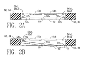
図1、図2A、及び図2Bは、本願発明のMEMSスイッチに設けられるシーソー部52、金属製電極54a及び54b、金属製スイッチ接点56a1,56a2,56b1及び56b2、及び金属製短絡バー58a及び58bを示す。シーソー部52は、好適には単結晶シリコン(Si)とされた材料からなる層62をマイクロマシニングすること(微細加工すること)によって形成される。層62の材料はまた、シーソー部52を好適に取り囲むフレーム64も形成している。一対のねじり棒部66a及び66b(図1中に点線で示されており、シーソー部52の両側からフレーム64に向かって外方に突出している)もまた、層62の材料からシーソー部52及びフレーム64とともにモノリシックに(一体に)形成されている。シーソー部52の寸法は、MEMSスイッチの特殊な構造に依存して変化するが、図の一実施形態においては、シーソー部52を取り囲むフレーム64を作り上げるために層62内に微細加工された開口部は、おおよそ約0.4×0.4ミリメートルの寸法である。この同じ図の実施形態では、層62はおおよそ17ミクロンの厚さであり、その一方で、シーソー部52は、おおよそ5ミクロンの厚さであり、ねじり棒部66a及び66bも同様である。
1, 2A, and 2B show a
ねじり棒部66a,66bは、シーソー部52を、該ねじり棒部66a,66bと同一直線上にある軸線68周りに回転するように周囲のフレーム64から支持している。数ミクロン厚の短絡バー58a,58bは、軸線68から最遠位のシーソー部52の両端で該シーソー部52に担持されている。ねじり棒部66a,66bは、上述の図の実施形態においては、おおよそ20ミクロン幅,60ミクロン長である。斯かる構成を有したねじり棒部66a,66bは硬く、そのために高い共鳴周波数を現し、これがかなり大きな復元力を与えて、この力によって、MEMSスイッチがスティクションを示そうとする度合いが低減される。さらに、ねじり棒部66a,66bの剛性は、結合されたシーソー部52とねじり棒部66a,66bがスイッチ動作速度を増加させるためのより高い共鳴周波数でのスイッチ動作速度に直接関与している。
The
上述の図の実施形態の場合、薄いチタン(Ti)接着層上にめっきされた数ミクロンの金(Au)が短絡バー58a,58bを形成している。短絡バー58a,58bは、おおよそ10ミクロン幅、40ミクロン長とされている。軸線68から最遠位のシーソー部52の両端にそれぞれ配置された一対の二酸化ケイ素(SiO2)絶縁パッド72a,72bが、短絡バー58a,58bをシーソー部52から電気的に絶縁するために、短絡バー58a,58bとシーソー部52との間に挿入されている。図1に示されているように、絶縁パッド72a,72bは、短絡バー58a,58bよりもシーソー部52上で大きな面積を覆っており、おおよそ1.0ミクロン厚とされている。シーソー部52に隣接するスイッチ接点56a1,56a2,56b1,56b2及び電極54a,54bは、おおよそ4.0ミクロン厚とされている。
In the case of the embodiment shown above, several micron gold (Au) plated on a thin titanium (Ti) adhesive layer forms the shorting
シーソー部52に外力が働かない場合は、ねじり棒部66a,66bによって与えられる復元力がシーソー部52を図2Aに描かれた姿勢位置に置こうとする。この位置に置かれると、シーソー部52は、隣接した電極54a,54b及びスイッチ接点56a1,56a2,56b1,56b2からおおよそ3ミクロン離間される。層62と電極54a,54bの一つとの間に電位差を与えると、電極(例えば図2Bの電極54a)に向かってシーソー部52が引き付けられるために、シーソー部52が軸線68周りに回転させられる。シーソー部52が十分回転することによって、短絡バー58a,58bの一方が、一対のスイッチ接点56a1,56a2,又は56b1,56b2(例えば図2Bのスイッチ接点56a1,56a2)に接触させられ、その結果、それらの間に電気回路ができる。
When no external force acts on the
以下に述べるように、図1、図2A及び図2Bに示されるように構成された、シーソー部52、電極54a,54b、スイッチ接点56a1,56a2,56b1,56b2、及び短絡バー58a,58bを有する本願発明に係るMEMSスイッチを組み立てるための種々異なるプロセスが存在するのであるが、好適なプロセスは、図3に示されるように開始される。図3は、基底ウェハ104上で1個のMEMSスイッチが占める領域102を示す。図3の実例では、線106は、中央の領域102と、隣接する8個の同一の領域102(これらの領域は、基底ウェハ104の縁に臨んだ部分を除けば、中央の領域102を取り囲んでいる)との境界を示している。以下の記載にあるように、MEMSスイッチが完成したのち、領域102は、線106に沿ったソーイングによって、個々のMEMSスイッチの領域に分割されることになる。
As will be described below, it has a
基底ウェハ104は、普通のシリコンウェハであり、ウェハ直径に関するSEMI規格準拠の厚さより薄いものとすることができる。例えば、基底ウェハ104が150mmの直径を有していれば、SEMI規格準拠のウェハであれば通常はおおよそ650ミクロンの厚さを有している。しかしながら、基底ウェハ104の厚さ(この厚さは、大幅に変更可能とされ、それでも本願発明に係るMEMSスイッチを作製するために有用足りえるものとされる)は、SEMI規格準拠のシリコンウェハより薄くすることができる。
The
本願発明に係る好ましい実施形態のMEMSスイッチの作製は、スイッチされる端子パッド用空洞部112、シーソー部用空洞部114、及び共通端子パッド用空洞部116を、基底ウェハ104の最上面108内に微細加工することから始まる。空洞部112,114及び116の深さは、厳密なものではないが、上述の図の実施形態の場合では、おおよそ10ミクロン深さとしなければならない。プラズマ装置、好適には、良好な均一性と異方性を与える反応性イオンエッチング(RIE:Reactive Ion Etch)が、空洞部112,114,116の微細加工に用いられる。しかしながら、KOHないし他のウェットエッチングもまた空洞部112,114,116を微細加工するのに用いることができる。標準的なエッチング阻止技術が空洞部112,114,116を微細加工する際に用いられる。それは、プラズマエッチング用のフォトレジストであったり、あるいはウェット(KOH)エッチング用の酸化ケイ素ないし窒化ケイ素によって形成されたマスクである。このマイクロマシニング(微細加工)によって、シーソー部用空洞部114が得られ、このシーソー部用空洞部114が、図2Bに図示されているようなシーソー部52の動きを受け入れ、その一方で、空洞部112,116が、以下に詳述されるように、フィードスルー又は電気的接点パッドを収容する。
Fabrication of a preferred embodiment MEMS switch according to the present invention involves switching the
上面108内に空洞部112,114,116を微細加工した後、どの図にも示されていないが、次のステップは、図3に示される基底ウェハ104の底面118内にアライメントマークをエッチングすることである。底側のアライメントマークは、後続のプロセシング作業を通じて空洞部112,114,116と他の微細加工された構造を揃えることができるように、基底ウェハ104内に微細加工された空洞部112,114,116に見当合わせされなければならない。この底側のアライメントマークは、全プロセスの流れの終わり近くの底面側のシリコンエッチング中にも用いられることになる。底面側アライメントマークは、空洞部112,114,116に揃えられた状態で、先ず特殊なターゲット専用マスクを用いたリソグラフィステップによって、そして次には基底ウェハ104の底面118を微細加工することによって形成される。ターゲット専用マスクのパターンは、基底ウェハ104の両面からフォトレジストを取り去る前に、底面118内へと数ミクロン深さでプラズマエッチングされる。MEMSスイッチを作製する際に赤外線の性能を有したアライナが使える場合には、底面側アライメントマーク作成は省くことができる。
After microfabrication of the
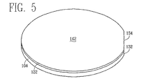
図4に示されたMEMSスイッチ製造の次のステップは、シリコン・オン・インシュレータ(SOI:silicon-on-insulator)ウェハ124の薄い単結晶Siデバイス層122を、基底ウェハ104の上面108に融着接合するというものである。好適にも、SOIウェハ124のデバイス層122は、極めて薄い二酸化ケイ素(SiO2)の埋め込み層上で17ミクロン厚とされ、そのため、その名前がシリコン・オン・インシュレータないしSOIとされている。シーソー部52及びねじり棒部66a,66bを微細加工する際に有利なSOIウェハ124の特徴は、デバイス層122が、薄いSiO2層132に対してSOIウェハ124の全表面上で略均一な厚さ(それも好ましくは約17ミクロン)を有していることである。SOIウェハ124のデバイス層122を基底ウェハ104の上面108に融着する際には、ウェハ104とウェハ124とは、基底ウェハ104上のアライメント用オリエンテーションフラット134を、対応するSOIウェハ124上のアライメント用オリエンテーションフラット136に合わせることで、大まかに揃えられる。基底ウェハ104へのSOIウェハ124の融着は、おおよそ1000℃で行なわれる。
The next step in fabricating the MEMS switch shown in FIG. 4 is to fuse a thin single crystal
基底ウェハ104とSOIウェハ124とが融着により一体に形成された後、基底ウェハ104の上面108に結合されたデバイス層122だけを残して、デバイス層122から最も遠い位置にあるハンドル層138、及び次のSiO2層132が取り除かれる。先ず、保護のための二酸化ケイ素層、窒化ケイ素層、これら両者の組み合わせ、もしくは他の任意の適した保護層が基底ウェハ104の底面118上に形成される。基底ウェハ104をこのようにマスクしたら、ハンドル層138のシリコンが、SOIウェハ124に対して行なわれるKOHエッチングによって取り除かれる。ハンドル層138を形成するシリコンのバルクが取り除かれて、埋め込まれたSiO2層132に達すると、KOHがSOIウェハ124をエッチングする速さがかなり遅くなる。このように、SiO2層132は、ハンドル層138を取り除くためのエッチストップとして機能する。ハンドル層138のバルクシリコンが取り除かれたら、前には埋もれていたが今や露出したSiO2層132がHFエッチングによって取り除かれる。その他のウェットなシリコンエッチング液、プラズマエッチング、研削及び研磨、あるいはこれらの方法の組み合わせを含め、ハンドル層138のバルクシリコンを除去する他の方法を用いることもできることに留意されたい。このプロセスが全て終了すると、図5に図示されたように、SOIウェハ124のデバイス層122だけが基底ウェハ104に結合された状態のままで残る。
After the
図6は、ハンドル層138とSiO2層132とがエッチングによって取り去られることで、デバイス層122の前面142として何が露出されたかを示している。空洞部112,114,116を形成するのと同じように、MEMSスイッチの好ましい実施形態を製造する次のステップは、おおよそ12.0ミクロン深さの初期空洞部144を、前面142を貫いてデバイス層122内へと微細加工(好適にはKOHエッチングを用いる)することである。MEMSならびに半導体製造の当業者には周知であるように、デバイス層122の前面142は、先ず酸化され、KOHを用いて初期空洞部144を微細加工するための遮蔽マスクが得られるようにパターンが形成される。次いで、初期空洞部144を微細加工した後に、残っているデバイス層122の前面142上の酸化物が除去される。図6に続く図では、初期空洞部144の壁部が垂直であるように示されているが、好適にもRIEプラズマエッチングよりむしろKOHエッチングを用いて壁部が形成されるために、従来よく知られているように、好ましい実施形態における初期空洞部144の壁部は、実際にはおおよそ54°の角度で傾いている。
FIG. 6 shows what is exposed as the
MEMSスイッチの好ましい実施形態においては、初期空洞部144の深さが、図2Aに図示された電極54a,54bの、シーソー部52から最も遠い表面と、シーソー部52の、電極54a,54bに最も近い表面との間のあきかたを決定する。初期空洞部144の深さは、シーソー部52上の短絡バー58a,58b及び電極54a,54bの金属及びスイッチ接点56a1,56a2,56b1,56b2の間の所望のギャップが得られるように、シーソー部52の所望の厚さとデバイス層122の所望の厚さを考慮に入れて算出される。
In a preferred embodiment of the MEMS switch, the depth of the
デバイス層122内に初期空洞部144を微細加工することで、初期空洞部144の底から上方に突出する4つの接地アイランド152(接地用孤立部)、U字形壁部154、さらにまたぎざぎざのU字形壁部156が残る。接地アイランド152及び壁部154,156は、上に向かって初期空洞部144の底からデバイス層122の前面142へと延出している。これら壁部154,156は、MEMSスイッチのシーソー部52となるべき前面142の床の部分を大部分取り囲んでいる。初期空洞部144の形成後、短絡バー58a,58bならびに初期空洞部144内の他の金属構造の堆積に備えてSiO2絶縁パッド72a,72bが初期空洞部144の床の上に堆積される。
By microfabricating the
図7及び図8は、短絡バー58a,58bを含めて、初期空洞部144の底に堆積される様々な金属構造部を示している。先に述べたように、これらの金属製の構造体は、最初に薄いTi接着層を堆積し、その上に続けて、図の実施形態ではおおよそ0.5ミクロンのAuを堆積させて形成することが好ましい。短絡バー58a,58bに加えて、一対の金属製の接地板162a,162bがそれぞれ延在して、初期空洞部144を横切り、短絡バー58a,58bならびに絶縁パッド72a,72bを超え、対になった接地アイランド152の間に拡がっている。0.5ミクロンのAu層を堆積した後、この金属部は、短絡バー58a,58bならびに接地板162a,162b用の形状が確定するように続いてリソグラフィによりパターン形成されてエッチングされる。その後、おおよそ4.0ミクロンの全厚となるように追加的なAuが短絡バー58a,58b上にめっきされる。
7 and 8 show various metal structures deposited on the bottom of the
全ての金属構造部が初期空洞部144内に作られたら、初期空洞部144の底に残っているデバイス層122の材料に穴をあける第2のRIEエッチングによって、ねじり棒部66a,66b及びシーソー部52の輪郭が描かれ、これによって軸線68の周りに回転するようにシーソー部52が自由になる。このようにして、シーソー部52及びねじり棒部66a,66bは、フレーム64になるデバイス層122の包囲材料とともにモノリシックに形成される。第2のRIEエッチングはまた、片持ちばり部166を下方に残しつつかつそれぞれの接地アイランド152を支持した状態にしながら、初期空洞部144を基底ウェハ104の空洞部112,116へと開口する。片持ちばり部166の自由端においてそれぞれの接地アイランド152を支持することによって、前面142より上側に突出している接地アイランド152の頂上における接地板162a,162bの終端部分でのAuの厚さが考慮される。片持ちばり部166に加わる従う力が、接地板162a,162bと以下に述べる後続の金属化(メタライゼーション)層との間の良好な電気的接触の形成を保証する。
Once all of the metal structure has been created in the
図9には、続いて図7に示されたデバイス層122の前面142にぴたりと合わされて融着されることになるパイレックス(登録商標)ガラス基板174のメタライゼーション表面172上の領域が示されている。ガラス基板174は、基底ウェハ104及びSOIウェハ124と同じ直径を有しており、好適には、1.0mmの厚さとされている。図9の例は、薄い1000Åのクロム−金(Cr‐Au)のシード層をメタライゼーション表面172上に堆積させた後のメタライゼーション表面172上部に存在する金属構造部を示すものである。Cr‐Auシード層をパターン形成することによって、好適な実施形態のMEMSスイッチの共通端子182、スイッチ接点56a1,56a2,56b1,56b2、及び電極54a,54bになるものに用いられる接点パッドと導体線とが構築される。また、Cr‐Auシード層をパターン形成することによって、接地アイランド152の突出している端部上に存在している接地板162a,162bの部分とぴたりと合わされるようにあてがわれる接地パッド186が構築される。上記構造部のためにCr‐Auシード層にパターンが作られたら、続いて、図9に表されたパターンを形成するようにおおよそ2.0ミクロンのAuがめっきされる。高い周波数の高周波(RF)信号を効果的に導くのに適した表皮効果条件を満足するように、スイッチ接点56a1,56a2,56b1,56b2及び共通端子182は、4.0ミクロン厚であることが好ましい。しかしながら、本願発明に係るスイッチは、上述されたものとは異なる材料及びプロセシングの工程が用いられるものであってもよい。
FIG. 9 shows a region on the
電極54a,54bは、該電極54a,54bとシーソー部52上における直接向き合った部分との間のギャップを低減するために、スイッチ接点56a1,56a2,56b1,56b2と同じ厚さでめっきされる。電極54a,54bと、シーソー部52上における直に向き合う部分との間のギャップがより小さくなることで、MEMSスイッチを駆動するために印加しなければならない電圧が低減する。
The
図10は、先に図3,図6,図7に図示された基底ウェハ104の部分を示す図であって、図9に図示されたガラス基板174のメタライゼーション表面172における対応部分がデバイス層122の前面142に陽極接合された後の基底ウェハ104の部分を示している。メタライゼーション表面172を前面142に接合する際には、図9に図示された金属パターンが、図7及び図8に見られるデバイス層122内に微細加工された構造に注意深く揃えられる。メタライゼーション表面172を前面142にこのように接合することで、図1,図2A及び図2Bに図示されるようなMEMSスイッチが構築される。図7及び図8に図示された構造では、電極54a,54bの接点パッドに接続している電極54a,54bのワイヤは、それぞれ壁部156内の鋸歯状の刻み目を通過し、その一方で、スイッチ接点56a1,56a2,56b1,56b2が、それぞれU字形の壁部154,156の腕の部分に沿って、接地板162a,162bにそれぞれ極めて近接した状態で延びている。
FIG. 10 is a diagram illustrating a portion of the
メタライゼーション表面172を174に陽極接合する間、接地アイランド152を支える片持ちばり部166は、各接地アイランド152頂上にある接地板162a,162bの金属と、ガラス基板174のメタライゼーション表面172上に形成された接地パッド186との間の干渉によって曲がる。片持ちばり部166を形成する単結晶シリコン材料の機械的な剛性が、接地パッド186と、接地アイランド152の位置において前記接地パッド186に対置された接地板162a,162bの部分との間の音響電気的な接続を確保する力を与える。
While anodizing the
ガラス基板174が壁部154に陽極接合された後、デバイス層122から最も離れているガラス基板174と基底ウェハ104の両方の外側部分全体が、図10に点線192,194で示されるように薄くされる。基底ウェハ104及びガラス基板174は、両側において研削及び研磨処理で薄くされることが好ましい。ガラス基板174がおおよそ100ミクロンの最終的な厚さを持つようにして、各層の約半分の厚さが除去される。組み合わされた基底ウェハ104、デバイス層122、及びガラス基板174を研削しかつ研磨することで、標準的な半導体デバイスの厚さに比肩し得る厚さを持ったMEMSスイッチが作り出される。基底ウェハ104とガラス基板174を薄くする際には、研削、研磨、化学機械平坦化(CMP:chemical mechanical planarization)、ないし種々のウェットエッチングやプラズマエッチングを含めて、MEMSないし半導体プロセシングに通常用いられるあらゆる技術を用いることができる。
After the
図11は、組み合わされた基底ウェハ104、デバイス層122、及びガラス基板174の断面を、図10で示したものを逆にした状態で示している。また、図11は、基底ウェハ104を薄くした後の空洞部112,116の基底にエッチング前には残っていた基底ウェハ104のシリコン材料を貫いてエッチングされた開口部を図示している。空洞部112,116を延長することは、先ず、両側アライナを用いてデバイス層122から最も離れている基底ウェハ104の底面側にパターンを作り上げ、さらに透明なガラス基板174を通してデバイス層122の構造を観察することによって行なわれる。次に、基底ウェハ104を形成しているシリコン材料がディープRIE装置を用いてプラズマエッチングされる。このように空洞部112,116を開口することで、電極54a,54bのための接点パッドと、スイッチ接点56a2,56b2のための共通端子182とともにスイッチ接点56a1,56b1と、陽極接合前にガラス基板174上にもともと形成されていた接地パッド186(図9に示されていて図11では点線で示されている)とが外に剥き出しになる。
FIG. 11 shows a cross section of the combined
図12は、組み合わされた基底ウェハ104、デバイス層122、及びガラス基板174を、この組体内部に同時に形成された多数のスイッチを別々にするためにソーイングした後の、そしてMEMSスイッチ内に備えられた接地パッド186と接点パッドに電気的なリード線198(図12には電気的なリード線198のうちの一本だけが示されている)をワイヤ接続した後の本願発明に係るMEMSスイッチの断面図である。
FIG. 12 shows the combined
電気的なリード線198は、一つが出力であるMEMSスイッチへの2つの入力信号を結合するための手段、又はこれとは別に、単一の入力信号を、MEMSスイッチからの2つの出力のいずれか一方、もしくはそれとは別の他方に結合するための手段を提供する。電気的なリード線198はまた、接地板162a,162bをシーソー部52ともども電気的に接地するための手段を提供し、さらには、シーソー部52に軸線68周りの回転を起させるシーソー部52と電極54a,54bとの間の電位に差を与えるための手段を提供する。
組み合わされた基底ウェハ104、デバイス層122、及びガラス基板174をソーイングすることによって、個別のMEMSスイッチ(典型的にはおおよそ2.0×1.5×1.5ミリメータ〔L×W×H〕とされている)が製造される。上記の寸法は、その大きさの2倍ないし2分の1の大きさに容易に変更することができる。組み合わされた基底ウェハ104、デバイス層122、及びガラス基板174のソーイング中、上方に向いた基底ウェハ104表面上の開放空洞部112,116は、従来のウェハテープによって覆われる。空洞部112,116をウェハテープで密封することは、底のところで接点パッドと接地パッド186が剥き出しとなった空洞部112,116の中に、そして、おそらくは、MEMSスイッチの内部にある短絡バー58a,58bとスイッチ接点56a1,56a2,56b1,56b2にさえもソー・スラリが入らないように保証する上で重要である。
By sawing the combined
必要であれば、あるいはその方がよければ、図7に示されたデバイス層122及び図9に示されたガラス基板174の表面を疎水性にすることによって、ソー・スラリのMEMSスイッチ内部への侵入に対する防壁部を作ることもできる。デバイス層122へのガラス基板174の陽極接合によって短絡バー58a,58b及びスイッチ接点56a1,56a2,56b1,56b2が作られているMEMSスイッチの内部と空洞部112,116との間の通路部は、おおよそ10ミクロン×100ミクロンとされている。これらの通路部の表面が疎水性であれば、その表面状態が、ソーイング中の水の侵入を防ぐことになる。ガラス基板174のメタライゼーション表面172を通路部に陽極接合する前に、あるいは空洞部112,116を開放するために上述の如く基底ウェハ104の背面側をエッチングした後に、表面をシリコーンで被覆することによって、上記の表面疎水性が作られる。表面をシリコーンで被覆するために用いることができる一つの方法としては、図7に示された組み合わされた基底ウェハ104及びデバイス層122、あるいは、図11に示された組み合わされた基底ウェハ104、デバイス層122、及びガラス基板174を、ゲルパック(Gel Pak)材料からなる加熱パッドとともに真空チャンバ内に配置するというものがある。ゲルパックパッドからのポリマの層をおおよそ40℃まで加熱するために熱板(ホットプレート)が用いられる。熱板が上記温度に達したら、組み合わされた基底ウェハ104及びデバイス層122及びゲルパックパッドが入っているチャンバが密閉され、真空引きされ、そしておおよそ4時間その状態に保たれる。その時間が経過したら、チャンバは先ずパージされ、次いで再び空気で満たされ、その後、後続のプロセシングのために組み合わされた基底ウェハ104及びデバイス層122が取り出される。組み合わされた基底ウェハ104及びデバイス層122をこのように処理することで、ソーイング中に空洞部112,116を通ってMEMSスイッチの内部に水が入ってくることが防止される。
If necessary or better, the surface of the
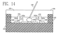
本願発明の他の実施形態には、スイッチ接点56a1,56a2,56b1,56b2、電極54a,54b、及び接地板162a,162bへの電気的な接続を行なうための様々な技術が主として含まれる。上記の接続を行なうための図13,14に図示された一つの代替技術は、空洞部112,116を開口するためにRIEエッチングを行なうのではなく、空洞部112,116の列に沿って基底ウェハ104の中へと、しかし貫通することなくソー切断部204の機械切削を行なうというものである。組み合わされた基底ウェハ104、デバイス層122、及びガラス基板174において直ぐ隣り合っているMEMSスイッチ同士の間の空け方や鋸歯の幅に合わせてソー切断部204を機械切削すれば、直ぐ隣り合っている一対のソー切断部204の間に突出するリッジ206を残すことも残さないこともできる。個別のMEMSスイッチを形成するために、組み合わされた基底ウェハ104、デバイス層122、及びガラス基板174を完全に貫くように後から切断しきってしまうことで、リッジ206が(もし残っているようなら)取り除かれる。ソー切断部204を機械切削すると、接点パッド及び接地パッドがソー・スラリに必ずさらされることになるために、この特殊な他の一実施形態の場合、空洞部112,116とMEMSスイッチの内部との間の通路部が、デバイス層122へのガラス基板174の陽極接合の前に疎水性にされることが不可欠である。上記の表面が上述のゲルパックの処置を用いることで疎水性にされることが好ましい。
Other embodiments of the present invention primarily include various techniques for making electrical connections to switch contacts 56a1, 56a2, 56b1, 56b2,
必要な電気的な接続を与えるための他の代替的な技術は、2つの主要な相違点があるものの、図10に示された基底ウェハ104とガラス基板174の薄層化を通してMEMSスイッチを製造するための先に上で述べたものと同じ工程をたどる。上記第1の相違点というのは、図3に示された空洞部112,116が、電気的な接点パッドのためには必要とされず、その代わりに接地アイランド152と片持ちばり部166のためだけにしか必要でないという点である。この他の一実施形態においては、接点パッド及び接地パッドは、ガラス基板174の外層上に配置されることになる。上記第2の相違点というのは、金属パターンが好ましい実施形態とは違ったものになり、それにより、ガラスウェハの両側で、金属製の相互接続部の2つの層を用いてRFパフォーマンスを最適化するようにするという点である。ガラス基板174をおおよそ50ミクロンの厚さにまで薄くした後、図15、図16に示されているように、バイア212が、接点パッド、接地パッド、及び電極のCrシード層までガラス基板174を貫通するようにしてエッチングされる。上記Crシード層は、図9に示された金属構造部を形成する際に堆積させた。上記ガラスは、8:1のHNO3:HFといったような等方性エッチング液を用いてウェットエッチングされるのが普通である。上記エッチング液は、Cr層に達すると同時に止まる。接点パッド、接地パッド、及び電極を形成する金属部が剥き出しにされたら、金属部214がバイア212内へと堆積されるとともに、ガラス基板174の表面の上側に堆積され、これにより、接点パッド、接地パッド、及び電極の金属部がガラス基板174の外側表面に広がることになる。金属部214は、図9に示された金属構造部を形成する際にガラス基板174上に堆積されたのと同じような、ガラス基板174上にスパッタリングないし蒸着されたクロム‐金(Cr-Au)の膜とされている。堆積されたCr‐Au膜は、内側にそれぞれ堆積された金属部214に隣接しかつ接続された接合パッド領域を残してパターン形成されてエッチングされる。続いて、追加のAuが、全厚でおおよそ4.0ミクロンとなるように上記金属部上にめっきされる。金属部214の接合パッド領域は、金属部214に接合されたワイヤを用いるか、あるいは、はんだ付け用バンプを用いることによってプリント回路基板に接続することができる。ガラス基板174の外部表面上に接合パッド領域が設けられるため、図11に図示されたような空洞部112,116を開口するための基底ウェハ104のRIEエッチングは、もはや必要ではない。従って、空洞部112,116を開口するためにRIEエッチングに必要とされた基底ウェハ104の裏側のパターン形成とエッチングは、この実施形態においては省略される。スイッチ接点56a1,56a2,56b1,56b2、電極54a,54b、及び接地板162a,162bへの電気的接続を形成するためのこの特殊な代替的な技術によって得られる一つの利点は、最終的に得られるMEMSスイッチが気密に密閉されていることである。
Another alternative technique for providing the necessary electrical connections is to produce a MEMS switch through thinning of the
図17ないし図20は、別の最後の実施形態を示している。この実施形態も、気密に密閉されたMEMSスイッチを提供する。この別の実施形態においては、先ず溝部222のパターンが、図17に示されるようにガラス基板174の表面224内におおよそ50ミクロンの深さでエッチングされる。次にCr‐Auのシード層が表面224上に堆積されてパターン形成され、これにより、おおよそ4.0ミクロン厚とされたAu導体226が続いて各溝部222内に形成可能となる。Au導体226は、スイッチ構造部、つまりMEMSスイッチの気密密閉された部分の内部のスイッチ接点56a1,56a2,56b1,56b2、電極54a,54b、及び接地板162a,162bから、MEMSスイッチの密閉された部分の外側にある接合パッド248へと電気的な信号を伝える。
17 to 20 show another final embodiment. This embodiment also provides a hermetically sealed MEMS switch. In this alternative embodiment, the pattern of
図18に示されるように、ガラス基板174の表面224は、次いで従来のシリコン支持ウェハ232に陽極接合され、ガラス基板174が100ミクロンまで薄くされる。図15,16に示された他の実施形態において上述したプロセス同様、次に、導体226のCrシード層に達するまでガラス基板174を貫くようにしてバイア242がエッチングされる。ガラスは、8:1のHNO3:HFといったような等方性エッチング液を用いてウェットエッチングされるのが普通である。上記エッチング液は、Cr層に達すると同時に止まる。導体226のCr層が剥き出しにされたら、金属部244がバイア242内へと堆積されるとともに、ガラス基板174のメタライゼーション表面172の上側に堆積され、これにより、導体226の金属部がガラス基板174のメタライゼーション表面172に拡がることになる。金属部244は、図9に示された金属構造部を形成する際にガラス基板174上に堆積されたのと同じようなスパッタリングないし蒸着されたクロム‐金(Cr-Au)の膜とされている。堆積されたCr‐Au膜は、パターン形成されてエッチングされ、電極54a,54b、スイッチ接点56a1,56a2,56b1,56b2、接地アイランド152頂上の接地板162a,162bのための接点端子、ならびに接合パッド248を形成する。続いて、追加のAuが、全厚でおおよそ4.0ミクロンとなるように上記金属部上にめっきされる。
As shown in FIG. 18, the
次に、図19に図示されるように、ガラス基板174のメタライゼーション表面172が、デバイス層122の前面142に陽極接合され、これにより、接合パッド248が、接合パッド空洞部252内のMEMSスイッチの他の残りから切り離されることになる。空洞部252(ソー切断部が引き続きMEMSスイッチを別々にしてしまうことなる場所の直ぐ隣に位置している)は、図6に示された空洞部112,114,116の微細加工と同時に基底ウェハ104内に形成され、図6の初期空洞部144の微細加工ならびにそれに続く図7のシーソー部52の解放と同時にデバイス層122を貫いて形成される。上記MEMSスイッチの好ましい実施形態と本実施形態との間の、初期空洞部144を形成する際の主な違いは、今や初期空洞部144が、図3に示された空洞部112,114,116に対応する3つの別々の空洞部に分離されていることである。図6に示された好ましい実施形態において開口部を有していた壁部154,156は、今や連続しており、そのために、初期空洞部144を3つの離れた空洞部に分離している。今や埋設された導体226は、壁部154,156の下で電気的な信号を伝える。それで、図13,図14に図示された他の実施形態と同様に、ソー切断部204は、基底ウェハ104内で空洞部252の列に沿って作られ、それにより、内部で隔離された接合パッド248を露にする。組み合わされた基底ウェハ104、デバイス層122、ガラス基板174及び支持ウェハ232を全て貫ききる後続のソーイングにより、個別のMEMSスイッチが作り出される。
Next, as illustrated in FIG. 19, the
図20は、内部に配置された接合パッド248、ガラス基板174を貫通するバイア242、及び溝部222内の導体226を有する一つの空洞部252を示している。図20の例はまた、電気的なリード線198、接合パッド248の一つに結合されたワイヤ示している。これとは別構成として、はんだ付けバンプを接合パッド248上に形成してもよい。
FIG. 20 shows one
本願発明を現在好ましい実施形態の観点から述べたが、斯かる開示は、純粋に例示にすぎず、限定として解釈されるべきでないことを理解されたい。例えば、シーソー部52を形成するための単結晶シリコン層は、好ましくはSOIウェハのデバイス層であるが、エピウェハ上のエピのN型最上層とすることもできる。シーソー部52から遠い方のねじり棒部66a,66bの端部が接合されるデバイス層122の材料は、シーソー部52を好適に取り囲むフレームを形成するが、本願発明に係るMEMSスイッチのシーソー部52は、デバイス層122の材料で囲まれていなくても構わない。MEMSスイッチ内に含まれる金属の導体部は、チタン(Ti)接着層に付与された金(AU)であることが好ましいが、それら導体部は、チタン(Ti)もしくはタングステン(W)上のプラチナ(Pt)といったようなあらゆる数の別の材料の組み合わせを使って作ることができよう。金属は、スパッタリング、電子ビーム堆積、ならびに蒸着を含めて、半導体プロセシングに用いられる任意の一般的な堆積法によって付着させることができる。
While the present invention has been described in terms of presently preferred embodiments, it is to be understood that such disclosure is purely exemplary and should not be construed as limiting. For example, the single crystal silicon layer for forming the
信号をMEMSスイッチ内につないだり、外へとつないだりするために、接点パッド及び接地パッド186に接続された電気的なリード線198を用いるのとは別の仕方も存在する。基底ウェハ104は、100ミクロンよりも薄い厚さに薄くすることができるので、電気的な信号は、別法として、接点パッド及び接地パッド186上に形成されたはんだ付けバンプ(solder bump)を用いて、MEMSスイッチの中へ、そして外へとつなげることができる。接点パッド及び接地パッド186上のはんだ付けバンプの存在によって、プリント回路基板上に存在する合わせはんだ付けバンプへのMEMSスイッチのフリップチップアタッチメントが可能になる。
There is an alternative to using
同様に、本明細書で開示された好ましい実施形態のMEMSスイッチは、シングルポール・ダブルスローリレイ(SPDT:single-pole double-throw)スイッチとされているが、2つの相互排他的なシングルポール・シングルスローリレイ(SPST:single-pole single-throw)スイッチとしての構成に容易に用いることができる。それで、上記の2つの相互排他的なSPSTスイッチは、MEMSスイッチ外側にある適宜接続された配線によってSPDTスイッチとして動作させるように構成することができる。加えて、スイッチ接点56a1,56a2,56b1,56b2及び2つの短絡バー58a,58bの代わりに、本願発明に係るSPDT‐MEMSスイッチは、スイッチ接点56a1,56b1だけを用い、そしてシーソー部52上に配置された導体によって互いに電気的に接続されている2つの短絡バー58a,58bを用いて構成することができる。MEMSスイッチのためのこのような構成においては、シーソー部52上の2つの短絡バー58a,58bを共に電気的に接続する導体は、延長することによってねじり棒部66a,66bの一方を横断する共通端子182につながっている。
Similarly, the preferred embodiment MEMS switch disclosed herein is a single-pole double-throw (SPDT) switch, although two mutually exclusive single-pole It can be easily used in a configuration as a single-throw relay (SPST) switch. Thus, the above two mutually exclusive SPST switches can be configured to operate as SPDT switches by appropriately connected wirings outside the MEMS switch. In addition, instead of the switch contacts 56a1, 56a2, 56b1, 56b2 and the two shorting
また、複数のシーソー部52は、該シーソー部に対応して設けられた電極54a,54b及びスイッチ接点56a1,56a2,56b1,56b2とともに、本願発明に係る単一のMEMSスイッチ内に組み込むことができる。2つのシーソー部52(それらシーソー部に対して設けられた電極54a,54b及びスイッチ接点56a1,56a2,56b1,56b2を有する)を用いると、シングルポール・フォースロー(SP4T:single-pole four-throw)MEMSスイッチを構成することができる。本願発明に係るMEMSスイッチがシャントスイッチとして動作するように外部配線を構成できるが、MEMSスイッチ自身は、短絡バー58a,58bをアースに接続することによってシャントスイッチとして動作するように構成することができる。斯かるシャントスイッチにおいては、スイッチ接点56a1,56a2,56b1,56b2は、図1及び図9に見られるギャップが無い連続した導体にすることができよう。
Further, the plurality of
従って、当業者であれば、上記の開示を読めば本発明の思想と観点から逸脱することなく、様々な変更、修正、及び/又は本発明の別の用途を間違いなく想到するであろう。それゆえ、請求項は、本発明の真の思想と観点の中に入るようなあらゆる変更、修正、あるいは別の用途を包含しているものと捉えられるべきである。 Accordingly, those of ordinary skill in the art will readily appreciate various changes, modifications, and / or other uses of the present invention without departing from the spirit and scope of the present invention after reading the above disclosure. Therefore, the claims should be construed to include any changes, modifications, or other uses that fall within the true spirit and scope of the present invention.
52 シーソー部
54a,54b 電極
56a1,56a2 スイッチ接点の第1の対
56b1,56b2 スイッチ接点の第2の対
58a,58b 短絡バー
64 フレーム
66a,66b ねじり棒部
68 軸線
104 基底ウェハ(基部)
122 デバイス層(微細加工されたモノリシック層)
152 接地アイランド(電気的接触アイランド)
162a,162b 接地板
166 片持ちばり部
174 基板(ガラス基板)
52
122 Device layer (microfabricated monolithic layer)
152 Grounding island (electrical contact island)
162a,
Claims (14)
内部に、
a.シーソー部;
b.前記シーソー部の両側に配置されかつ前記シーソー部に連結されて前記シーソー部がその周りに回転可能とされる一つの軸線を決定する一対のねじり棒部;及び
c.前記シーソー部から遠い側における前記ねじり棒部の端部が連結されて前記ねじり棒部によって決まる前記軸線周りに回転させるために前記ねじり棒部を介して前記シーソー部を支持するフレーム;
を微細加工した材料からなるモノリシック層と;
前記ねじり棒部によって決定される前記回転軸線から遠位の前記シーソー部の端部で保持された導電性を有する第1の短絡バーと;
前記モノリシック層の第1の表面に取り付けられた基部と;さらに、
前記基部が取り付けられた前記モノリシック層の前記第1の表面から遠い側の前記モノリシック層の第2の表面に接合された基板であって、
該基板上に、
a.前記ねじり棒部によって決定される前記回転軸線の片側にある前記シーソー部の表面に対して対置された第1の電極であって、該第1の電極と前記シーソー部との間に電位を与えることで、前記ねじり棒部によって決定される前記回転軸線の周りに前記シーソー部を第1の方向に回転させる第1の電極;及び
b.前記第1の入力用導体に対して、そして前記第1の出力用導体に対して、それぞれ接続可能となるように設けられたスイッチ接点の第1の対であって:
i.前記シーソー部に力が加わっていないときには、前記第1の短絡バーに隣接しているが該第1の短絡バーから離間された状態で配置されており;
ii.前記シーソー部に力が加わっていないときには、互いに電気的に絶縁されており;さらに、
iii.前記ねじり棒部によって決定される前記回転軸線周りに前記シーソー部を前記第1の方向に回転させる十分強い力が前記シーソー部に加わると前記第1の短絡バーがつなぎ合せる;
スイッチ接点の第1の対;
を形成した基板と;
を備え、
前記第1の短絡バーが前記スイッチ接点の第1の対に接触する程に、前記ねじり棒部によって決定される前記回転軸線周りに前記シーソー部が前記第1の方向に回転すると、前記接続を行なう第1の短絡バーが前記スイッチ接点の第1の対とともに電気的に連結するように構成されているMEMSスイッチ。 An integrated microelectromechanical system (MEMS) switch, wherein an electrical signal present on a first input conductor connected to the MEMS switch is also output to a first output connected to the MEMS switch. In a MEMS switch provided to selectively couple to a conductor,
Inside,
a. Seesaw part;
b. A pair of torsion bar portions disposed on opposite sides of the seesaw portion and connected to the seesaw portion to determine one axis around which the seesaw portion is rotatable; and c. A frame for supporting the seesaw portion via the torsion bar portion so that the end of the torsion bar portion on the side far from the seesaw portion is connected and rotated around the axis determined by the torsion bar portion;
A monolithic layer made of a microfabricated material;
A first shorting bar having conductivity held at the end of the seesaw portion distal to the axis of rotation determined by the torsion bar;
A base attached to the first surface of the monolithic layer; and
A substrate bonded to the second surface of the monolithic layer on the side remote from the first surface of the monolithic layer to which the base is attached,
On the substrate,
a. A first electrode opposed to the surface of the seesaw portion on one side of the rotation axis determined by the torsion bar, and applying a potential between the first electrode and the seesaw portion A first electrode for rotating the seesaw portion in a first direction about the axis of rotation determined by the torsion bar portion; and b. A first pair of switch contacts provided to be connectable to the first input conductor and to the first output conductor, respectively:
i. When no force is applied to the seesaw portion, the seesaw portion is disposed adjacent to the first shorting bar but separated from the first shorting bar;
ii. When no force is applied to the seesaw portions, they are electrically insulated from each other;
iii. The first shorting bar joins when a sufficiently strong force is applied to the seesaw portion to rotate the seesaw portion in the first direction around the rotation axis determined by the torsion bar portion;
A first pair of switch contacts;
A substrate formed with;
With
When the seesaw portion rotates in the first direction around the rotation axis determined by the torsion bar portion so that the first shorting bar contacts the first pair of the switch contacts, the connection is made. A MEMS switch configured to have a first shorting bar to perform electrically connect with the first pair of switch contacts.
前記シーソー部は、前記第1の短絡バーとは前記回転軸線を挟んで反対の側にある前記シーソー部の端部に第2の短絡バーを保持し;さらに、
前記基板が、同じく該基板上に:
a.前記第2の入力用導体に対して、そして前記第2の出力用導体に対して、それぞれ接続可能となるように設けられたスイッチ接点の第2の対であって:
i.前記シーソー部に力が加わっていないときには、前記第2の短絡バーに隣接しているが該第2の短絡バーから離間された状態で配置されており;
ii.前記シーソー部に力が加わっていないときには、互いに電気的に絶縁されており;さらに、
iii.前記ねじり棒部によって決定される前記回転軸線周りに前記シーソー部を、前記第1の方向とは逆の前記第2の方向に回転させる十分強い力が前記シーソー部に加わると前記第2の短絡バーがつなぎ合わせる;
スイッチ接点の第2の対
を形成し、
前記第2の短絡バーが前記スイッチ接点の第2の対に接触する程に、前記ねじり棒部によって決定される前記回転軸線周りに前記シーソー部が前記第2の方向に回転すると、前記接続を行なう第2の短絡バーが前記スイッチ接点の第2の対とともに電気的に連結するように構成されているMEMSスイッチ。 2. The MEMS switch according to claim 1, wherein an electrical signal existing on a second input conductor side connected to the MEMS switch is applied to a second output conductor also connected to the MEMS switch. In a MEMS switch further provided to selectively couple:
The seesaw portion holds a second shorting bar at an end of the seesaw portion on the opposite side of the rotation axis from the first shorting bar;
The substrate is also on the substrate:
a. A second pair of switch contacts provided to be connectable to the second input conductor and to the second output conductor, respectively:
i. When no force is applied to the seesaw portion, the seesaw portion is disposed adjacent to the second shorting bar but separated from the second shorting bar;
ii. When no force is applied to the seesaw portions, they are electrically insulated from each other;
iii. When a sufficiently strong force to rotate the seesaw portion around the rotation axis determined by the torsion rod portion in the second direction opposite to the first direction is applied to the seesaw portion, the second short circuit is performed. The bars join together;
Forming a second pair of switch contacts,
When the seesaw portion rotates in the second direction about the rotation axis determined by the torsion bar portion, the connection is made so that the second short-circuit bar contacts the second pair of switch contacts. A MEMS switch configured to electrically couple a second shorting bar to perform with the second pair of switch contacts.
前記シーソー部は、前記第1の短絡バーとは前記回転軸線を挟んで反対の側にある前記シーソー部の端部に第2の短絡バーを保持し;さらに、
前記基板が、同じく該基板上に:
a.スイッチ接点の第2の対、それも、そのうち一つの第1のスイッチ接点が、第2の入力用導体にそれぞれ接続可能となるように設けられるとともに、そのうち一つの第2のスイッチ接点が、前記第1の出力用導体に接続可能となるように設けられた該スイッチ接点の第2の対の一方に接続されたスイッチ接点の第2の対であって:
i.前記シーソー部に力が加わっていないときには、前記第2の短絡バーに隣接しているが該第2の短絡バーから離間された状態で配置されており;
ii.前記シーソー部に力が加わっていないときには、互いに電気的に絶縁されており;さらに、
iii.前記ねじり棒部によって決定される前記回転軸線周りに前記シーソー部を、前記第1の方向とは逆の前記第2の方向に回転させる十分強い力が前記シーソー部に加わると前記第2の短絡バーがつなぎ合わせる;
スイッチ接点の第2の対
を形成し、
前記第2の短絡バーが前記スイッチ接点の第2の対に接触する程に、前記ねじり棒部によって決定される前記回転軸線周りに前記シーソー部が前記第2の方向に回転すると、前記接続を行なう第2の短絡バーが前記スイッチ接点の第2の対とともに電気的に連結するように構成されているMEMSスイッチ。 The MEMS switch according to claim 1, wherein an electrical signal existing on a second input conductor side connected to the MEMS switch is selectively transmitted to the first output conductor connected to the MEMS switch. In a MEMS switch further provided to couple to:
The seesaw portion holds a second shorting bar at an end of the seesaw portion on the opposite side of the rotation axis from the first shorting bar;
The substrate is also on the substrate:
a. A second pair of switch contacts is provided such that one of the first switch contacts is connectable to the second input conductor, and one of the second switch contacts is the aforementioned switch contact. A second pair of switch contacts connected to one of the second pair of switch contacts provided to be connectable to a first output conductor, wherein:
i. When no force is applied to the seesaw portion, the seesaw portion is disposed adjacent to the second shorting bar but separated from the second shorting bar;
ii. When no force is applied to the seesaw portions, they are electrically insulated from each other;
iii. When a sufficiently strong force to rotate the seesaw portion around the rotation axis determined by the torsion rod portion in the second direction opposite to the first direction is applied to the seesaw portion, the second short circuit is performed. The bars join together;
Forming a second pair of switch contacts,
When the seesaw portion rotates in the second direction about the rotation axis determined by the torsion bar portion, the connection is made so that the second short-circuit bar contacts the second pair of switch contacts. A MEMS switch configured to electrically couple a second shorting bar to perform with the second pair of switch contacts.
前記基板は、該基板上に、スイッチ接点と入力用導体ならびに出力用導体との間において電気的な信号をそれぞれ伝送する導電体を形成し、
前記導電体に隣接して配置されているとともに該導電体から電気的に絶縁された接地板を備えているMEMSスイッチ。 The MEMS switch according to claim 1, wherein:
The board forms a conductor on the board for transmitting an electrical signal between the switch contact and the input conductor and the output conductor,
A MEMS switch comprising a ground plate disposed adjacent to the conductor and electrically insulated from the conductor.
前記第2の層内に設けられた片持ちばり部を備え;さらに、
同じく前記第2の層内に設けられて前記片持ちばり部の自由端において支持された電気的接触アイランドを備え、該電気的接触アイランドが、前記片持ちばり部から遠位の該電気的接触アイランドの端部において前記第2の層上に配置された前記導電体の一部を保持し、前記電気的接触アイランドの前記端部における前記導電体の前記一部が、前記片持ちばり部によって加えられる力によって、前記第1の層上に配置された導電体と密接に接触させられるMEMS電気的接触構造体。 A microelectromechanical system (MEMS) provided to make electrical contact between a conductor disposed on a first layer of the MEMS device and a conductor disposed on a second layer of the MEMS device. ) An electrical contact structure,
A cantilever portion provided in the second layer;
An electrical contact island also provided in the second layer and supported at a free end of the cantilever, the electrical contact island being distal to the cantilever A portion of the conductor disposed on the second layer is held at an end of the island, and the portion of the conductor at the end of the electrical contact island is held by the cantilever A MEMS electrical contact structure that is brought into intimate contact with a conductor disposed on the first layer by an applied force.
同じく一つの導電体が上に配置された第2の層を備え、
前記第2の層は、
a.片持ちばり部;及び
b.前記片持ちばり部の自由端において支持された電気的接触アイランドを備え、前記電気的接触アイランドが、前記片持ちばり部から遠位の該電気的接触アイランドの端部において、前記第2の層上に配置された前記導電体の一部を保持し、前記電気的接触アイランドの前記端部における前記導電体の前記一部が、前記片持ちばり部によって加えられる力によって、前記第1の層上に配置された導電体と密接に接触させられる微小電気機械システム(MEMS)構造体。
A first layer with one conductor disposed thereon; and a second layer also having a conductor disposed thereon;
The second layer is
a. A cantilever; and b. An electrical contact island supported at a free end of the cantilever, wherein the electrical contact island is at the end of the electrical contact island distal from the cantilever. Holding the portion of the conductor disposed thereon, the portion of the conductor at the end of the electrical contact island by the force applied by the cantilevered portion, the first layer; A micro electro mechanical system (MEMS) structure that is in intimate contact with a conductor disposed thereon.
Applications Claiming Priority (4)
| Application Number | Priority Date | Filing Date | Title |
|---|---|---|---|
| US40131102P | 2002-08-03 | 2002-08-03 | |
| US41532502P | 2002-10-02 | 2002-10-02 | |
| US44295803P | 2003-01-29 | 2003-01-29 | |
| PCT/US2003/024255 WO2004013898A2 (en) | 2002-08-03 | 2003-08-04 | Sealed integral mems switch |
Publications (2)
| Publication Number | Publication Date |
|---|---|
| JP2006515953A true JP2006515953A (en) | 2006-06-08 |
| JP2006515953A5 JP2006515953A5 (en) | 2006-09-21 |
Family
ID=31499336
Family Applications (1)
| Application Number | Title | Priority Date | Filing Date |
|---|---|---|---|
| JP2005506093A Pending JP2006515953A (en) | 2002-08-03 | 2003-08-04 | Sealed integrated MEMS switch |
Country Status (6)
| Country | Link |
|---|---|
| US (1) | US7123119B2 (en) |
| EP (1) | EP1547189A4 (en) |
| JP (1) | JP2006515953A (en) |
| KR (1) | KR100997929B1 (en) |
| AU (1) | AU2003258020A1 (en) |
| WO (1) | WO2004013898A2 (en) |
Cited By (3)
| Publication number | Priority date | Publication date | Assignee | Title |
|---|---|---|---|---|
| WO2008069202A1 (en) * | 2006-12-07 | 2008-06-12 | Omron Corporation | High frequency relay and its connection structure |
| JP2011501460A (en) * | 2007-10-25 | 2011-01-06 | コーニンクレッカ フィリップス エレクトロニクス エヌ ヴィ | Polarized light emitting device |
| JP2011129369A (en) * | 2009-12-17 | 2011-06-30 | Fujifilm Corp | Piezo-electric mems switch and method for manufacturing the same |
Families Citing this family (63)
| Publication number | Priority date | Publication date | Assignee | Title |
|---|---|---|---|---|
| US20060232365A1 (en) * | 2002-10-25 | 2006-10-19 | Sumit Majumder | Micro-machined relay |
| US7275292B2 (en) * | 2003-03-07 | 2007-10-02 | Avago Technologies Wireless Ip (Singapore) Pte. Ltd. | Method for fabricating an acoustical resonator on a substrate |
| US7190245B2 (en) | 2003-04-29 | 2007-03-13 | Medtronic, Inc. | Multi-stable micro electromechanical switches and methods of fabricating same |
| US7388459B2 (en) | 2003-10-28 | 2008-06-17 | Medtronic, Inc. | MEMs switching circuit and method for an implantable medical device |
| KR100530010B1 (en) * | 2003-11-13 | 2005-11-22 | 한국과학기술원 | Low-voltage and low-power toggle type - SPDT(Single Pole Double Throw) rf MEMS switch actuated by combination of electromagnetic and electrostatic forces |
| EP1756848A4 (en) * | 2004-04-12 | 2009-12-23 | Siverta Inc | Single-pole, double-throw mems switch |
| US7615833B2 (en) * | 2004-07-13 | 2009-11-10 | Avago Technologies Wireless Ip (Singapore) Pte. Ltd. | Film bulk acoustic resonator package and method of fabricating same |
| US7521363B2 (en) * | 2004-08-09 | 2009-04-21 | Analog Devices, Inc. | MEMS device with non-standard profile |
| US7388454B2 (en) | 2004-10-01 | 2008-06-17 | Avago Technologies Wireless Ip Pte Ltd | Acoustic resonator performance enhancement using alternating frame structure |
| US8981876B2 (en) | 2004-11-15 | 2015-03-17 | Avago Technologies General Ip (Singapore) Pte. Ltd. | Piezoelectric resonator structures and electrical filters having frame elements |
| US7202560B2 (en) | 2004-12-15 | 2007-04-10 | Avago Technologies Wireless Ip (Singapore) Pte. Ltd. | Wafer bonding of micro-electro mechanical systems to active circuitry |
| US7791434B2 (en) | 2004-12-22 | 2010-09-07 | Avago Technologies Wireless Ip (Singapore) Pte. Ltd. | Acoustic resonator performance enhancement using selective metal etch and having a trench in the piezoelectric |
| KR100661350B1 (en) * | 2004-12-27 | 2006-12-27 | 삼성전자주식회사 | Mems devices package and method for manufacturing thereof |
| JP4417861B2 (en) * | 2005-01-31 | 2010-02-17 | 富士通株式会社 | Micro switching element |
| US7369013B2 (en) | 2005-04-06 | 2008-05-06 | Avago Technologies Wireless Ip Pte Ltd | Acoustic resonator performance enhancement using filled recessed region |
| US7611919B2 (en) * | 2005-04-21 | 2009-11-03 | Hewlett-Packard Development Company, L.P. | Bonding interface for micro-device packaging |
| US7528691B2 (en) * | 2005-08-26 | 2009-05-05 | Innovative Micro Technology | Dual substrate electrostatic MEMS switch with hermetic seal and method of manufacture |
| US7737807B2 (en) | 2005-10-18 | 2010-06-15 | Avago Technologies Wireless Ip (Singapore) Pte. Ltd. | Acoustic galvanic isolator incorporating series-connected decoupled stacked bulk acoustic resonators |
| GB0523713D0 (en) * | 2005-11-22 | 2005-12-28 | Cavendish Kinetics Ltd | Enclosure method |
| JP2007149370A (en) * | 2005-11-24 | 2007-06-14 | Fujitsu Media Device Kk | Switch |
| KR100697652B1 (en) | 2005-12-01 | 2007-03-20 | 주식회사 에이스테크놀로지 | RF Switch |
| JP4628275B2 (en) * | 2006-01-31 | 2011-02-09 | 富士通株式会社 | Microswitching device and method for manufacturing microswitching device |
| US7746677B2 (en) | 2006-03-09 | 2010-06-29 | Avago Technologies Wireless Ip (Singapore) Pte. Ltd. | AC-DC converter circuit and power supply |
| US7479685B2 (en) | 2006-03-10 | 2009-01-20 | Avago Technologies General Ip (Singapore) Pte. Ltd. | Electronic device on substrate with cavity and mitigated parasitic leakage path |
| US8120133B2 (en) * | 2006-09-11 | 2012-02-21 | Alcatel Lucent | Micro-actuator and locking switch |
| JP4855233B2 (en) * | 2006-12-07 | 2012-01-18 | 富士通株式会社 | Microswitching device and method for manufacturing microswitching device |
| ITTO20060907A1 (en) | 2006-12-20 | 2008-06-21 | St Microelectronics Srl | PROCESS OF MANUFACTURE OF A MICROELECTRANCANICAL INTERACTION SYSTEM FOR A STORAGE SUPPORT |
| US7732977B2 (en) | 2008-04-30 | 2010-06-08 | Avago Technologies Wireless Ip (Singapore) | Transceiver circuit for film bulk acoustic resonator (FBAR) transducers |
| US7855618B2 (en) | 2008-04-30 | 2010-12-21 | Avago Technologies Wireless Ip (Singapore) Pte. Ltd. | Bulk acoustic resonator electrical impedance transformers |
| DE102008043790B4 (en) * | 2008-11-17 | 2017-04-06 | Robert Bosch Gmbh | Micromechanical component |
| JP2012528335A (en) * | 2009-05-27 | 2012-11-12 | キング アブドゥーラ ユニバーシティ オブ サイエンス アンド テクノロジー | MEMS mass-spring-damper system using out-of-plane suspension system |
| US8248185B2 (en) | 2009-06-24 | 2012-08-21 | Avago Technologies Wireless Ip (Singapore) Pte. Ltd. | Acoustic resonator structure comprising a bridge |
| US8902023B2 (en) | 2009-06-24 | 2014-12-02 | Avago Technologies General Ip (Singapore) Pte. Ltd. | Acoustic resonator structure having an electrode with a cantilevered portion |
| JP5398411B2 (en) * | 2009-08-10 | 2014-01-29 | 株式会社東芝 | Micro movable device and manufacturing method of micro movable device |
| US8193877B2 (en) | 2009-11-30 | 2012-06-05 | Avago Technologies Wireless Ip (Singapore) Pte. Ltd. | Duplexer with negative phase shifting circuit |
| US8796904B2 (en) | 2011-10-31 | 2014-08-05 | Avago Technologies General Ip (Singapore) Pte. Ltd. | Bulk acoustic resonator comprising piezoelectric layer and inverse piezoelectric layer |
| US9243316B2 (en) | 2010-01-22 | 2016-01-26 | Avago Technologies General Ip (Singapore) Pte. Ltd. | Method of fabricating piezoelectric material with selected c-axis orientation |
| US8962443B2 (en) | 2011-01-31 | 2015-02-24 | Avago Technologies General Ip (Singapore) Pte. Ltd. | Semiconductor device having an airbridge and method of fabricating the same |
| US9425764B2 (en) | 2012-10-25 | 2016-08-23 | Avago Technologies General Ip (Singapore) Pte. Ltd. | Accoustic resonator having composite electrodes with integrated lateral features |
| US9154112B2 (en) | 2011-02-28 | 2015-10-06 | Avago Technologies General Ip (Singapore) Pte. Ltd. | Coupled resonator filter comprising a bridge |
| US9048812B2 (en) | 2011-02-28 | 2015-06-02 | Avago Technologies General Ip (Singapore) Pte. Ltd. | Bulk acoustic wave resonator comprising bridge formed within piezoelectric layer |
| US9083302B2 (en) | 2011-02-28 | 2015-07-14 | Avago Technologies General Ip (Singapore) Pte. Ltd. | Stacked bulk acoustic resonator comprising a bridge and an acoustic reflector along a perimeter of the resonator |
| US9203374B2 (en) | 2011-02-28 | 2015-12-01 | Avago Technologies General Ip (Singapore) Pte. Ltd. | Film bulk acoustic resonator comprising a bridge |
| US9136818B2 (en) | 2011-02-28 | 2015-09-15 | Avago Technologies General Ip (Singapore) Pte. Ltd. | Stacked acoustic resonator comprising a bridge |
| US9148117B2 (en) | 2011-02-28 | 2015-09-29 | Avago Technologies General Ip (Singapore) Pte. Ltd. | Coupled resonator filter comprising a bridge and frame elements |
| US9490418B2 (en) | 2011-03-29 | 2016-11-08 | Avago Technologies General Ip (Singapore) Pte. Ltd. | Acoustic resonator comprising collar and acoustic reflector with temperature compensating layer |
| US8575820B2 (en) | 2011-03-29 | 2013-11-05 | Avago Technologies General Ip (Singapore) Pte. Ltd. | Stacked bulk acoustic resonator |
| US9490771B2 (en) | 2012-10-29 | 2016-11-08 | Avago Technologies General Ip (Singapore) Pte. Ltd. | Acoustic resonator comprising collar and frame |
| US9444426B2 (en) | 2012-10-25 | 2016-09-13 | Avago Technologies General Ip (Singapore) Pte. Ltd. | Accoustic resonator having integrated lateral feature and temperature compensation feature |
| US9401692B2 (en) | 2012-10-29 | 2016-07-26 | Avago Technologies General Ip (Singapore) Pte. Ltd. | Acoustic resonator having collar structure |
| US8350445B1 (en) | 2011-06-16 | 2013-01-08 | Avago Technologies Wireless Ip (Singapore) Pte. Ltd. | Bulk acoustic resonator comprising non-piezoelectric layer and bridge |
| US8922302B2 (en) | 2011-08-24 | 2014-12-30 | Avago Technologies General Ip (Singapore) Pte. Ltd. | Acoustic resonator formed on a pedestal |
| US8940586B2 (en) * | 2011-11-23 | 2015-01-27 | Taiwan Semiconductor Manufacturing Co., Ltd. | Mechanism for MEMS bump side wall angle improvement |
| US9165723B2 (en) | 2012-08-23 | 2015-10-20 | Harris Corporation | Switches for use in microelectromechanical and other systems, and processes for making same |
| US9053874B2 (en) | 2012-09-20 | 2015-06-09 | Harris Corporation | MEMS switches and other miniaturized devices having encapsulating enclosures, and processes for fabricating same |
| US9053873B2 (en) | 2012-09-20 | 2015-06-09 | Harris Corporation | Switches for use in microelectromechanical and other systems, and processes for making same |
| US8907849B2 (en) | 2012-10-12 | 2014-12-09 | Harris Corporation | Wafer-level RF transmission and radiation devices |
| US9203133B2 (en) | 2012-10-18 | 2015-12-01 | Harris Corporation | Directional couplers with variable frequency response |
| US9385684B2 (en) | 2012-10-23 | 2016-07-05 | Avago Technologies General Ip (Singapore) Pte. Ltd. | Acoustic resonator having guard ring |
| US9330874B2 (en) * | 2014-08-11 | 2016-05-03 | Innovative Micro Technology | Solder bump sealing method and device |
| US10376444B2 (en) * | 2016-03-22 | 2019-08-13 | International Business Machines Corporation | Secure medication delivery |
| US11083837B2 (en) | 2016-03-22 | 2021-08-10 | International Business Machines Corporation | Secure medication delivery |
| CN106771667B (en) * | 2016-12-29 | 2019-05-03 | 西北核技术研究所 | Method for microwave measurement and measuring system based on the rotation of the phase heart |
Citations (8)
| Publication number | Priority date | Publication date | Assignee | Title |
|---|---|---|---|---|
| JPH052977A (en) * | 1991-06-25 | 1993-01-08 | Matsushita Electric Works Ltd | Electrostatic relay |
| JPH052978A (en) * | 1991-06-25 | 1993-01-08 | Matsushita Electric Works Ltd | Electrostatic relay |
| JPH0714479A (en) * | 1993-03-29 | 1995-01-17 | Seiko Epson Corp | Substrate conducting device and pressure detecting device, and fluid delivery device and ink jet head employing the devices |
| JPH0917483A (en) * | 1995-06-27 | 1997-01-17 | Yokogawa Electric Corp | Electrode lead-out structure for micro-machine device |
| JPH09180616A (en) * | 1995-12-28 | 1997-07-11 | Omron Corp | Electrostatic relay and its manufacture |
| JPH11273529A (en) * | 1998-03-20 | 1999-10-08 | Nec Corp | High-frequency relay |
| JP2001076605A (en) * | 1999-07-01 | 2001-03-23 | Advantest Corp | Integrated microswitch and its manufacture |
| WO2002058092A1 (en) * | 2001-01-18 | 2002-07-25 | Arizona State University | Micro-magnetic latching switch with relaxed permanent magnet alignment requirements |
Family Cites Families (25)
| Publication number | Priority date | Publication date | Assignee | Title |
|---|---|---|---|---|
| US5278368A (en) * | 1991-06-24 | 1994-01-11 | Matsushita Elec. Works, Ltd | Electrostatic relay |
| US5173055A (en) * | 1991-08-08 | 1992-12-22 | Amp Incorporated | Area array connector |
| US5619061A (en) * | 1993-07-27 | 1997-04-08 | Texas Instruments Incorporated | Micromechanical microwave switching |
| US6044705A (en) * | 1993-10-18 | 2000-04-04 | Xros, Inc. | Micromachined members coupled for relative rotation by torsion bars |
| US5488862A (en) * | 1993-10-18 | 1996-02-06 | Armand P. Neukermans | Monolithic silicon rate-gyro with integrated sensors |
| US6426013B1 (en) * | 1993-10-18 | 2002-07-30 | Xros, Inc. | Method for fabricating micromachined members coupled for relative rotation |
| JP3465940B2 (en) * | 1993-12-20 | 2003-11-10 | 日本信号株式会社 | Planar type electromagnetic relay and method of manufacturing the same |
| JP3182301B2 (en) * | 1994-11-07 | 2001-07-03 | キヤノン株式会社 | Microstructure and method for forming the same |
| US5578976A (en) * | 1995-06-22 | 1996-11-26 | Rockwell International Corporation | Micro electromechanical RF switch |
| US5861549A (en) * | 1996-12-10 | 1999-01-19 | Xros, Inc. | Integrated Silicon profilometer and AFM head |
| WO1997026527A1 (en) * | 1996-01-22 | 1997-07-24 | Xros, Inc. | Vane-type micromachined silicon micro-flow meter |
| EP1012890A4 (en) * | 1997-04-01 | 2000-06-28 | Xros Inc | Adjusting operating characteristics of micromachined torsional oscillators |
| EP0892419B1 (en) * | 1997-07-18 | 2005-11-16 | Northrop Grumman Corporation | Micro electro-mechanical system (MEMS) switch |
| DE19823690C1 (en) * | 1998-05-27 | 2000-01-05 | Siemens Ag | Micromechanical electrostatic relay |
| US6154176A (en) * | 1998-08-07 | 2000-11-28 | Sarnoff Corporation | Antennas formed using multilayer ceramic substrates |
| US6392220B1 (en) * | 1998-09-02 | 2002-05-21 | Xros, Inc. | Micromachined members coupled for relative rotation by hinges |
| US6410360B1 (en) * | 1999-01-26 | 2002-06-25 | Teledyne Industries, Inc. | Laminate-based apparatus and method of fabrication |
| US6069540A (en) * | 1999-04-23 | 2000-05-30 | Trw Inc. | Micro-electro system (MEMS) switch |
| US6307169B1 (en) * | 2000-02-01 | 2001-10-23 | Motorola Inc. | Micro-electromechanical switch |
| US6384353B1 (en) * | 2000-02-01 | 2002-05-07 | Motorola, Inc. | Micro-electromechanical system device |
| DE10004393C1 (en) | 2000-02-02 | 2002-02-14 | Infineon Technologies Ag | micro-relay |
| US6535091B2 (en) * | 2000-11-07 | 2003-03-18 | Sarnoff Corporation | Microelectronic mechanical systems (MEMS) switch and method of fabrication |
| KR100387239B1 (en) * | 2001-04-26 | 2003-06-12 | 삼성전자주식회사 | MEMS Relay and fabricating method thereof |
| US6701779B2 (en) * | 2002-03-21 | 2004-03-09 | International Business Machines Corporation | Perpendicular torsion micro-electromechanical switch |
| KR100451409B1 (en) * | 2002-10-15 | 2004-10-06 | 한국전자통신연구원 | Micro-optical switch and method for manufacturing the same |
-
2003
- 2003-08-04 US US10/523,532 patent/US7123119B2/en not_active Expired - Fee Related
- 2003-08-04 JP JP2005506093A patent/JP2006515953A/en active Pending
- 2003-08-04 EP EP03767105A patent/EP1547189A4/en not_active Withdrawn
- 2003-08-04 KR KR1020057001977A patent/KR100997929B1/en not_active IP Right Cessation
- 2003-08-04 WO PCT/US2003/024255 patent/WO2004013898A2/en active Application Filing
- 2003-08-04 AU AU2003258020A patent/AU2003258020A1/en not_active Abandoned
Patent Citations (8)
| Publication number | Priority date | Publication date | Assignee | Title |
|---|---|---|---|---|
| JPH052977A (en) * | 1991-06-25 | 1993-01-08 | Matsushita Electric Works Ltd | Electrostatic relay |
| JPH052978A (en) * | 1991-06-25 | 1993-01-08 | Matsushita Electric Works Ltd | Electrostatic relay |
| JPH0714479A (en) * | 1993-03-29 | 1995-01-17 | Seiko Epson Corp | Substrate conducting device and pressure detecting device, and fluid delivery device and ink jet head employing the devices |
| JPH0917483A (en) * | 1995-06-27 | 1997-01-17 | Yokogawa Electric Corp | Electrode lead-out structure for micro-machine device |
| JPH09180616A (en) * | 1995-12-28 | 1997-07-11 | Omron Corp | Electrostatic relay and its manufacture |
| JPH11273529A (en) * | 1998-03-20 | 1999-10-08 | Nec Corp | High-frequency relay |
| JP2001076605A (en) * | 1999-07-01 | 2001-03-23 | Advantest Corp | Integrated microswitch and its manufacture |
| WO2002058092A1 (en) * | 2001-01-18 | 2002-07-25 | Arizona State University | Micro-magnetic latching switch with relaxed permanent magnet alignment requirements |
Cited By (4)
| Publication number | Priority date | Publication date | Assignee | Title |
|---|---|---|---|---|
| WO2008069202A1 (en) * | 2006-12-07 | 2008-06-12 | Omron Corporation | High frequency relay and its connection structure |
| US8421561B2 (en) | 2006-12-07 | 2013-04-16 | Omron Corporation | High frequency relay and its connection structure |
| JP2011501460A (en) * | 2007-10-25 | 2011-01-06 | コーニンクレッカ フィリップス エレクトロニクス エヌ ヴィ | Polarized light emitting device |
| JP2011129369A (en) * | 2009-12-17 | 2011-06-30 | Fujifilm Corp | Piezo-electric mems switch and method for manufacturing the same |
Also Published As
| Publication number | Publication date |
|---|---|
| WO2004013898A2 (en) | 2004-02-12 |
| AU2003258020A1 (en) | 2004-02-23 |
| US7123119B2 (en) | 2006-10-17 |
| KR20050083613A (en) | 2005-08-26 |
| EP1547189A2 (en) | 2005-06-29 |
| AU2003258020A8 (en) | 2004-02-23 |
| EP1547189A4 (en) | 2006-11-08 |
| US20050206483A1 (en) | 2005-09-22 |
| KR100997929B1 (en) | 2010-12-02 |
| WO2004013898A3 (en) | 2004-06-10 |
Similar Documents
| Publication | Publication Date | Title |
|---|---|---|
| JP2006515953A (en) | Sealed integrated MEMS switch | |
| EP3642611B1 (en) | Microfabricated ultrasonic transducer having individual cells with electrically isolated electrode sections | |
| US7242066B2 (en) | Manufacturing method of a microelectromechanical switch | |
| JP5189491B2 (en) | Wafer level packaging method | |
| EP1760036B1 (en) | MEMS device having contact and standoff bumps and method of actuating | |
| JP2007159389A (en) | Piezoelectric type rf-mems element and its method of manufacturing | |
| JP3918559B2 (en) | Electrostatic relay and communication equipment using the relay | |
| US6621135B1 (en) | Microrelays and microrelay fabrication and operating methods | |
| TW200534354A (en) | A fabrication method for making a planar cantilever, low surface leakage, reproducible and reliable metal dimple contact micro-relay mems switch, and a microelectromechanical device having a common ground plane layer and set of contact teeth and method | |
| TW200947490A (en) | Mem switch and method for manufacturing the same | |
| CN102569306A (en) | Electromechanical transducer and method of manufacturing the same | |
| JP2007535797A (en) | Beam for micromachine technology (MEMS) switches | |
| EP1672661A2 (en) | MEMS switch and method of fabricating the same | |
| US20080217149A1 (en) | Integrated arrangement and method for production | |
| US7816999B2 (en) | Single-pole double-throw MEMS switch | |
| US7463125B2 (en) | Microrelays and microrelay fabrication and operating methods | |
| US20050062565A1 (en) | Method of using a metal platform for making a highly reliable and reproducible metal contact micro-relay MEMS switch | |
| KR100668614B1 (en) | Piezoelectric driven resistance?type RF MEMS switch and manufacturing method thereof | |
| US7208339B2 (en) | Process for manufacturing a micromachined oscillating element, in particular a mirror for optical switches | |
| Chiao et al. | MEMS reconfigurable antennas | |
| US20180155184A1 (en) | Bondline for mm-wave applications | |
| US20020097118A1 (en) | Current actuated switch | |
| Pranonsatit et al. | Rotary RF MEMS switch based on the wobble motor principle | |
| CN101123321A (en) | Sealed integral MEMS switch | |
| JP3836809B2 (en) | Micromachine manufacturing method |
Legal Events
| Date | Code | Title | Description |
|---|---|---|---|
| A521 | Written amendment |
Free format text: JAPANESE INTERMEDIATE CODE: A523 Effective date: 20060301 |
|
| A521 | Written amendment |
Free format text: JAPANESE INTERMEDIATE CODE: A523 Effective date: 20060804 |
|
| A621 | Written request for application examination |
Free format text: JAPANESE INTERMEDIATE CODE: A621 Effective date: 20060804 |
|
| A131 | Notification of reasons for refusal |
Free format text: JAPANESE INTERMEDIATE CODE: A131 Effective date: 20081028 |
|
| A521 | Written amendment |
Free format text: JAPANESE INTERMEDIATE CODE: A523 Effective date: 20090128 |
|
| A131 | Notification of reasons for refusal |
Free format text: JAPANESE INTERMEDIATE CODE: A131 Effective date: 20090804 |
|
| A601 | Written request for extension of time |
Free format text: JAPANESE INTERMEDIATE CODE: A601 Effective date: 20091104 |
|
| A602 | Written permission of extension of time |
Free format text: JAPANESE INTERMEDIATE CODE: A602 Effective date: 20091111 |
|
| A131 | Notification of reasons for refusal |
Free format text: JAPANESE INTERMEDIATE CODE: A131 Effective date: 20100817 |
|
| A601 | Written request for extension of time |
Free format text: JAPANESE INTERMEDIATE CODE: A601 Effective date: 20101117 |
|
| A602 | Written permission of extension of time |
Free format text: JAPANESE INTERMEDIATE CODE: A602 Effective date: 20101125 |
|
| A02 | Decision of refusal |
Free format text: JAPANESE INTERMEDIATE CODE: A02 Effective date: 20110412 |