JP2006512956A - Hook fastener component having switch circuit - Google Patents
Hook fastener component having switch circuit Download PDFInfo
- Publication number
- JP2006512956A JP2006512956A JP2004565934A JP2004565934A JP2006512956A JP 2006512956 A JP2006512956 A JP 2006512956A JP 2004565934 A JP2004565934 A JP 2004565934A JP 2004565934 A JP2004565934 A JP 2004565934A JP 2006512956 A JP2006512956 A JP 2006512956A
- Authority
- JP
- Japan
- Prior art keywords
- hook
- loop fastener
- component
- switch circuit
- electrical
- Prior art date
- Legal status (The legal status is an assumption and is not a legal conclusion. Google has not performed a legal analysis and makes no representation as to the accuracy of the status listed.)
- Withdrawn
Links
Images


Classifications
-
- A—HUMAN NECESSITIES
- A44—HABERDASHERY; JEWELLERY
- A44B—BUTTONS, PINS, BUCKLES, SLIDE FASTENERS, OR THE LIKE
- A44B18/00—Fasteners of the touch-and-close type; Making such fasteners
- A44B18/0046—Fasteners made integrally of plastics
- A44B18/0061—Male or hook elements
- A44B18/0065—Male or hook elements of a mushroom type
Landscapes
- Adhesives Or Adhesive Processes (AREA)
- Slide Fasteners, Snap Fasteners, And Hook Fasteners (AREA)
- Adhesive Tapes (AREA)
Abstract
本発明は、例えばフック、茸頭片またはループ等の多数の面ファスナー要素(2)を有する面ファスナー部品(1、101、201、301)であって、面ファスナー部品(1、101、201、301)が平面的基材(3、103、203、303)を有し、面ファスナー要素(2)が基材(3、103、203、303)の少なくとも一方の面(4)から張り出しているものにおいて、面ファスナー部品(1、101、201、301)がスイッチ回路(5、305)を有し、このスイッチ回路が少なくとも1つの電気部品および/または電子部品(6、106;7、107、207、307)を有することを特徴とする面ファスナー部品に関する。The present invention relates to a hook-and-loop fastener component (1, 101, 201, 301) having a number of hook-and-loop fastener elements (2) such as hooks, wharves or loops, 301) has a planar substrate (3, 103, 203, 303) and a hook-and-loop fastener element (2) projects from at least one surface (4) of the substrate (3, 103, 203, 303). In one, the hook-and-loop fastener component (1, 101, 201, 301) has a switch circuit (5, 305), the switch circuit comprising at least one electrical component and / or electronic component (6, 106; 7, 107, 207, 307).
Description
本発明は、請求項1の前文に係る面ファスナー部品に関する。
The present invention relates to a hook-and-loop fastener component according to the preamble of
このような面ファスナー部品が例えば特許文献1により公知である。ふつう2つの互いに作用結合可能な面ファスナー部品から形成される面ファスナーはしばしば繊維製またはその他の衣服類において利用され、ベルクロファスナーの名称でも知られている。他の応用分野は、例えば車両工学において内装材要素の固着または一般に脱離可能な固着実現のための例えば組立技術である。
本発明の課題は、面ファスナー部品および面ファスナーの機能性を高めることである。 The subject of this invention is improving the functionality of a hook_and_loop | surface fastener component and a hook_and_loop | surface fastener.
この課題は、請求項1に明示された面ファスナー部品によって解決される。本発明の特別な実施形態は従属請求項に明示されている。
This problem is solved by the hook-and-loop fastener part specified in
この課題は、例えばフック、茸頭片またはループ等の多数の面ファスナー要素を有する面ファスナー部品であって、面ファスナー部品が平面的基材を有し、面ファスナー要素が基材の少なくとも一方の面から張り出しているものにおいて、面ファスナー部品がスイッチ回路を有し、このスイッチ回路が少なくとも1つの電気部品および/または電子部品を有することによって解決される。 The problem is a hook-and-loop fastener part having a number of hook-and-loop fastener elements such as hooks, wharves or loops, the hook-and-loop fastener part having a planar substrate, and the hook-and-loop fastener element being at least one of the substrates. In the overhang, the surface fastener part has a switch circuit, which is solved by having at least one electrical component and / or electronic component.
基材および/または面ファスナー要素は主にプラスチックから製造されている。プラスチックは例えば熱可塑的に成形可能であり、面ファスナー要素の製造には特許文献1による方法が応用される。熱可塑性プラスチックの代わりに熱硬化性プラスチック、ポリマープラスチック、アクリルプラスチックまたはその他の好適なプラスチックも使用することができる。面ファスナー要素は主に基材と一体に構成されている。そうする代わりに面ファスナー要素は特許文献2に述べられたように特に塗布装置で製造しておくこともでき、この塗布装置によって面ファスナー要素は連続的に与えられる小滴で構成される。
The substrate and / or the hook-and-loop fastener element are mainly made of plastic. The plastic can be molded, for example, thermoplastically, and the method according to
本発明の特別な1実施形態において電気部品および/または電子部品は平面的基材に、上におよび/または内に配置されている。部品が基材の表面に配置されている限り、これは面ファスナー要素のない領域で行うことができる。特に面ファスナー要素は基材の片面にのみ配置し、基材の反対側の側面上に部品を配置しておくことができる。その都度の応用事例に依存して部品は面ファスナー要素間または要素上に配置しておくこともできる。 In a special embodiment of the invention, the electrical and / or electronic components are arranged on, on and / or in a planar substrate. As long as the part is placed on the surface of the substrate, this can be done in the area without the hook-and-loop element. In particular, the hook-and-loop fastener element can be arranged only on one side of the substrate, and the parts can be arranged on the opposite side surface of the substrate. Depending on the particular application case, the parts can also be arranged between or on the hook-and-loop fastener elements.
部品が平面的基材に一体化されている限り、これは混成式に、または一体式にさえ、行うことができ、特に基材もしくはその材料自体は電気的および/または電子的機能性を有することができる。例えば基材用に相応するプラスチックを使用する場合、導体路を用意するために、場合によっては局所的に限定された電気伝導性を予定することができる。選択的にまたは補足的に基材も、少なくとも局所的に限定された半導体特性を有することができ、回路技術的インテリジェンスを平面的基材に一体化可能である。 As long as the component is integrated into the planar substrate, this can be done in a hybrid manner or even in an integral manner, in particular the substrate or the material itself has electrical and / or electronic functionality. be able to. For example, when using a corresponding plastic for the substrate, a locally limited electrical conductivity can be planned in some cases in order to prepare the conductor track. Alternatively or additionally, the substrate can also have at least locally limited semiconductor properties, and circuit technology intelligence can be integrated into the planar substrate.
好ましい一実施形態において部品は厚膜技術または薄膜技術で平面的基材上に被着されている。例えば電気導体路は構造化または非構造化被覆、例えば印刷、析出または蒸着によって基材上に設けておくことができる。包装技術の方から例えばアルミニウム被覆包装フィルムが知られているが、包装フィルムにおいてアルミニウム被覆はまったく別の目的のために、つまり拡散障壁として設けられている。相応する印刷技術もしくは被覆技術を利用して、少なくとも領域によっては構造化したアルミニウムウェブ、またはその他の導電性材料からなる導体路を比較的簡単に基材上に用意することができる。 In a preferred embodiment, the component is deposited on a planar substrate using thick film technology or thin film technology. For example, the electrical conductor track can be provided on the substrate by a structured or unstructured coating, such as printing, deposition or vapor deposition. For example, an aluminum coated packaging film is known from the packaging art, but in the packaging film the aluminum coating is provided for a completely different purpose, ie as a diffusion barrier. By means of a corresponding printing or coating technique, it is possible to relatively easily prepare a conductor track made of a structured aluminum web, or at least some other conductive material, on a substrate.
こうして、例えば面ファスナー部品に対する力の印加を信号で知らせる電気式センサを用意することもできる。これにより、例えば車両シート用表皮材を固着するのに利用される面ファスナー部品は同時に、人間が車両シートに着座したか否かを電気信号で知らせることができ、それに応じて車両のベルトテンショナまたはエアバッグ等の安全装置を制御することができる。 In this way, for example, an electric sensor that notifies the application of force to the hook-and-loop fastener component by a signal can be prepared. As a result, for example, a hook-and-loop fastener component used for fixing a vehicle seat skin material can simultaneously notify whether or not a person is seated on the vehicle seat with an electric signal, and accordingly, a vehicle belt tensioner or Safety devices such as airbags can be controlled.
実質的に導体路によって形成されるこのように単純な電気式センサに留まらず、ほぼ任意の複雑なセンサ、アクチュエータ、データ処理電子装置を基材上に実現する可能性がある。これに加えて例えば電子式センサおよび/または集積半導体部品を基材にまたは基材内に設けておくことができる。電気部品および/または電子部品の少なくとも一部は、面ファスナー要素の平面的基材に積層されもしくは平面的基材と結合された他の基材上に被着しておくこともできる。 In addition to such a simple electrical sensor formed substantially by a conductor track, almost any complex sensor, actuator, and data processing electronics may be realized on the substrate. In addition, for example, electronic sensors and / or integrated semiconductor components can be provided on or in the substrate. At least a portion of the electrical and / or electronic components can also be deposited on another substrate that is laminated to or bonded to the planar substrate of the hook and loop element.
本発明に係る面ファスナー部品によって例えばいわゆるスマートラベルを実現することができ、スマートラベルはインテリジェントラベルとして面ファスナー部品の機械的機能性に基づいて簡単にかつ任意の頻度で再剥離可能に衣服類、対象物等に取付可能である。 For example, a so-called smart label can be realized by the hook-and-loop fastener part according to the present invention, and the smart label is an intelligent label that can be easily peeled off at any frequency based on the mechanical functionality of the hook-and-loop fastener part, It can be attached to an object.
特別な一実施形態において集積半導体部品は電子データ記憶装置を有する。これは読取専用記憶装置(ROM)やプログラマブル読取専用記憶装置(PROM)とすることもできる。特に消去可能なプログラマブル読取専用記憶装置(EPROM)や電気的消去書込み可能な読取専用記憶装置(EEPROM)であれば有効である。データ記憶装置内に例えば識別データまたは許可データを記憶することができる。例えば安全技術上重要な部屋、車両、諸機能等に対するアクセス認証をこのようなデータ記憶装置内に格納しておくことができる。 In one particular embodiment, the integrated semiconductor component has an electronic data storage device. This can also be a read only memory (ROM) or a programmable read only memory (PROM). In particular, an erasable programmable read-only storage device (EPROM) or an electrically erasable and writable read-only storage device (EEPROM) is effective. For example, identification data or authorization data can be stored in the data storage device. For example, access authentication for rooms, vehicles, functions, etc. that are important in terms of safety technology can be stored in such a data storage device.
選択的にまたは補足的に、人間の生物学的特徴、特に個人的な特徴を保存することができる。これは特徴及び個人的な特色を記憶し保存するために使用される。このような面ファスナー部品は例えば、この面ファスナー部品によって相応するアクセス認証を有する相応に許可された人間の衣服に脱離可能に簡単に取付けることができる。 Alternatively or additionally, human biological characteristics, in particular personal characteristics, can be preserved. This is used to store and store features and personal features. Such a hook-and-loop fastener part can be easily removably attached, for example, to a correspondingly authorized human garment having a corresponding access authorization.
これに関連して、データ記憶装置に記憶されたデータを非接触式に読み出すことができると特別有利である。面ファスナー部品は主に、相応する電子問合せに答えて、いずれにしても記憶データの一部を送信する一種の応答機を形成する。付属する読出ステーションは定置式とすることもできるし、携帯式とすることもできる。 In this connection, it is particularly advantageous if the data stored in the data storage device can be read out in a contactless manner. The hook-and-loop fastener component mainly forms a kind of responder that responds to a corresponding electronic inquiry and in any case transmits a part of the stored data. The attached reading station can be stationary or portable.
面ファスナー部品と読出ステーションとの間での情報伝送に必要なエネルギーは電磁場によって非接触式に面ファスナー部品内のスイッチ回路に入力することができる。このためスイッチ回路が少なくとも1つの受信コイルを有し、この受信コイルは例えば相応に構造化された導体路によって形成しておくこともできる。 The energy required for information transmission between the hook-and-loop fastener component and the reading station can be input to the switch circuit in the hook-and-loop fastener component in a non-contact manner by an electromagnetic field. For this purpose, the switch circuit can have at least one receiving coil, which can be formed, for example, by a correspondingly structured conductor track.
選択的にまたは補足的にスイッチ回路はエネルギー溜、特に、電池または充電可能な蓄電池の態様の電気化学的エネルギー溜を有することができる。選択的にまたは補足的に容量式またはその他のエネルギー溜も利用することができる。エネルギー溜も主に薄膜技術または厚膜技術で実施されており、面ファスナー部品は全体として僅かな厚さを有する。 Alternatively or additionally, the switch circuit can have an energy reservoir, in particular an electrochemical energy reservoir in the form of a battery or a rechargeable battery. Alternatively or additionally, capacitive or other energy reservoirs can be utilized. The energy reservoir is also mainly implemented by thin film technology or thick film technology, and the surface fastener component has a slight thickness as a whole.
主にデータ記憶装置内に非接触式にもデータが記憶可能でもあり、記憶装置から情報を読み出すことができるだけでなく、新たな、場合によっては更新された情報を記憶装置に書き込むこともできる。この書込み過程も主に非接触式に行われ、読出し過程と同様に、面ファスナー部品と読出し装置との間に直接的な視覚上の接触を必要としない。別の応用分野から知られている通信システムにおいて、達成可能な通信到達距離は1メートル以下またはそれ以上である。到達距離は送信器の出力および/または書込み/読取装置のアンテナ寸法によって実質的に決まる。面ファスナー部品に一体化されたエネルギー溜を利用すると基本的に一層大きな到達距離を達成できる。 Data can be stored mainly in a non-contact manner in the data storage device, and not only can information be read from the storage device, but also new and possibly updated information can be written to the storage device. This writing process is also mainly performed in a non-contact manner and does not require direct visual contact between the hook-and-loop fastener component and the reading device, as in the reading process. In communication systems known from other applications, the achievable communication range is 1 meter or less. The reach is substantially determined by the output of the transmitter and / or the antenna size of the writer / reader. By using the energy reservoir integrated with the hook-and-loop fastener component, basically a larger reach can be achieved.
このようなインテリジェント面ファスナー部品の応用分野はごく広範に広がっており、特に、従来は面ファスナー部品が利用されなかった応用も実現できる。面ファスナー部品の機械的機能性は、人間もしくはその衣服類または対象物に電子インテリジェンスを簡単にかつ反復可能に取付けまた引き剥がすことを可能とする。情報伝送が視覚上の接触を必要としないので、面ファスナー部品は、例えば衣服の内面または対象物の目視可能でない側面上に隠して配置しておくこともできる。 The field of application of such intelligent hook-and-loop fastener parts is extremely widespread, and in particular, applications where no hook-and-loop fastener parts are conventionally used can be realized. The mechanical functionality of the hook-and-loop fastener component allows electronic intelligence to be easily and repeatably attached to and removed from a person or their garments or objects. Since information transmission does not require visual contact, the hook-and-loop fastener component can be hidden and placed, for example, on the inner surface of the garment or on the non-visible side of the object.
本発明のその他の利点、特徴および細部は従属請求項と以下の明細書から明らかとなり、以下の明細書では図面を参考に幾つかの実施例が詳しく説明される。特許請求の範囲および明細書で触れられた特徴はそれぞれ個々にそれ自体としてまたは任意に組合せても発明にとって本質的たり得る。 Other advantages, features and details of the invention will become apparent from the dependent claims and the following specification, in which several embodiments are described in detail with reference to the drawings. Each feature mentioned in the claims and specification can be essential to the invention either individually or in any combination.
図1は本発明に係る面ファスナー部品1を備えた面ファスナーの横断面図である。面ファスナー部品は行と列とに規則的に配置される多数の面ファスナー要素2を有し、面ファスナー要素は平面的基材3と一体に熱可塑的に成形可能なプラスチックから形成されており、基材3の一方の面4から斜めに、主に直角に張り出している。面ファスナー要素2とは反対の面上に面ファスナー部品1がスイッチ回路5を有し、図示実施例においてこのスイッチ回路は導体路6の態様の電気部品も集積半導体部品7の態様の電子部品も有する。
FIG. 1 is a cross-sectional view of a hook-and-loop fastener provided with a hook-and-
導体路6は構造化アルミニウム被覆によって基材3の面ファスナー要素2とは反対の側面上に形成されている。半導体部品7の接続電極との接続は接続突起8、いわゆるバンプを介して行われる。半導体部品7の機能と複雑性はその都度の応用事例に適合されている。例えば半導体部品7は実質的に温度センサで構成することができ、場合によっては、例えば所定の温度値を上まわりまたは下まわるとき、求めた温度値を規則的にまたは事象に起因して記憶するための記憶装置をなお備えている。このため半導体部品7が部分領域にデータ記憶装置17を有し、このデータ記憶装置から主に非接触式にデータを読み出すことができ、また主にやはり非接触式にデータを書き込むことができる。これらのデータは導体路6を介して面ファスナー部品1の外側へと送ることができる。別の応用事例において半導体部品7は例えば応答機一式を含むことができ、この応答機は非接触式に相応する書込み/読出し装置と識別データを交信する。
The conductor track 6 is formed on the side surface of the
本発明により装備した面ファスナー部品1は面ファスナー要素2を利用して機械的に強固に、但し脱離可能に、その機械的機能性に関して実質同一に構成される他の面ファスナー部品9と、相対応する面ファスナー要素2、10の係合によって結合させることができる。他の面ファスナー部品9は繊維製またはその他の衣服11に縫い付け、貼り付けまたはその他の仕方で強固に、ふつう脱離不能に被着しておくことができる。それゆえ、本発明により装備した面ファスナー部品1は脱離可能に衣服11に固定することができる。従って、本発明により装備した面ファスナー部品1は従来の面ファスナーの機械的固着可能性を電気部品および/または電子部品の多かれ少なかれ複雑な制御機能と組み合わせ、従ってスマートファスナーまたはインテリジェント面ファスナーと称することができる。
The hook-and-
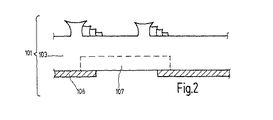
図2は本発明の第2実施例を示す。面ファスナー部品101はやはり熱可塑的に成形可能な基材103を有し、この基材に半導体部品107が一体化されている。この一体化は混成態様で、例えば基材103に相応に設けられまたは押し込まれた凹部に半導体部品107を挿入することによって実施しておくことができる。基材103もしくはそれに付属する材料の諸可能性および特性に依存して制御インテリジェンスは一体式に基材103の材料に、例えば基材103の場合によっては局所的に限定された半導体領域に適切に影響を及ぼすことによって、実現することもできる。一体式または混成式に一体化された電子部品107のボンディングはやはり導体路106を通して行われ、この場合導体路は基材103の相応する表面の構造化被覆によって製造されている。 FIG. 2 shows a second embodiment of the present invention. The hook-and-loop fastener component 101 also has a base material 103 that can be molded thermoplastically, and a semiconductor component 107 is integrated with the base material. This integration can be carried out in a hybrid manner, for example by inserting the semiconductor component 107 into a recess provided correspondingly or pressed into the substrate 103. Depending on the possibilities and properties of the substrate 103 or the materials attached to it, the control intelligence can be integrated into the material of the substrate 103 in one piece, for example in the case of the substrate 103 in some locally limited semiconductor regions. It can also be realized by influencing. Bonding of the integrated or hybrid integrated electronic component 107 is again performed through the conductor track 106, in which case the conductor track is produced by a structured coating on the corresponding surface of the substrate 103.
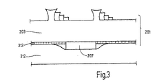
図3は本発明の第3実施例を示す。電子部品207は、接着剤層213によって面ファスナー要素201の平面的基材203に積層された他の基材212上に被着されている。
FIG. 3 shows a third embodiment of the present invention. The
図4は本発明の第4実施例を示す。図の中央に配置された本発明に係る面ファスナー部品301の面ファスナー要素302とは反対の面にスイッチ回路305が配置されており、この面でもって面ファスナー部品は強固かつ脱離不能に繊維布カバー314に固定されており、この布カバーは例えば車両シートパッドのカバー用に使用することができる。面ファスナー要素302とは反対の面上に面ファスナー部品301は相突接する導体路306a、306bを有する。面ファスナー部品301は面ファスナー要素302を利用して繊維布カバー314と一緒に脱離可能にパッド部品315に固定可能であり、このためパッド部品は相応する他の面ファスナー部品309を有する。
FIG. 4 shows a fourth embodiment of the present invention. A
例えば車両シートに着座した人間によって矢印316の方向で力Fが作用すると、パッド部品315が、従って面ファスナー部品301も、多かれ少なかれ強く撓み、特に導体路306a、306bの間の距離もしくは突接個所が変化することになる。それに伴って、直接的にまたは基材303に一体化された電子部品307を介して間接的に面ファスナー部品301の外側へと交信できる電気接触抵抗が変化する。電子部品307は非接触式交信用部品および/または他の制御インテリジェンスもしくは他のセンサの実装を選択できるよう設けられているにすぎない。特にセンサ機能は電子半導体部品307なしでも面ファスナー部品301内に設けておくことができ、例えば圧力センサまたは湿度センサも導体路の相応する櫛状配置によって実現される。
For example, when a force F acts in the direction of
半導体部品307のすぐ横に、または場合によってはそれから空間的に離間しても、但し電気的にそれと接続されて、面ファスナー部品301は薄膜技術または厚膜技術のエネルギー溜318、主に電池または再充電可能な蓄電池の態様の電気化学的エネルギー溜318を有する。
The hook-and-
導体路は金属層の構造化または非構造化被着によって実現することができ、例えば気相からの蒸着または析出等の非構造化被着の場合、引き続く構造化は機械式、化学式またはその他の仕方で行うことができる。本発明に係る面ファスナー部品1、101、201、301用に使用されるすべての材料、特に使用済みプラスチックは主にリサイクル可能および/または生物学的に分解可能である。
Conductor tracks can be realized by structured or unstructured deposition of the metal layer, for example in the case of unstructured deposition such as vapor deposition or deposition from the gas phase, subsequent structuring can be mechanical, chemical or other Can be done in a way. All materials used for the hook-and-
Claims (14)
Applications Claiming Priority (2)
| Application Number | Priority Date | Filing Date | Title |
|---|---|---|---|
| DE10301424A DE10301424B3 (en) | 2003-01-13 | 2003-01-13 | Burr fastener material, especially for automobile seat covers, incorporates a circuit with at least one electrical/electronic component and a memory, to register occupancy and signal the safety belt condition |
| PCT/EP2003/011283 WO2004062415A1 (en) | 2003-01-13 | 2003-10-11 | Adhesive closing device provided with a switching circuit |
Publications (2)
| Publication Number | Publication Date |
|---|---|
| JP2006512956A true JP2006512956A (en) | 2006-04-20 |
| JP2006512956A5 JP2006512956A5 (en) | 2011-08-04 |
Family
ID=30775634
Family Applications (1)
| Application Number | Title | Priority Date | Filing Date |
|---|---|---|---|
| JP2004565934A Withdrawn JP2006512956A (en) | 2003-01-13 | 2003-10-11 | Hook fastener component having switch circuit |
Country Status (7)
| Country | Link |
|---|---|
| US (1) | US7847195B2 (en) |
| EP (1) | EP1583438B1 (en) |
| JP (1) | JP2006512956A (en) |
| DE (1) | DE10301424B3 (en) |
| DK (1) | DK1583438T3 (en) |
| ES (1) | ES2566564T3 (en) |
| WO (1) | WO2004062415A1 (en) |
Families Citing this family (2)
| Publication number | Priority date | Publication date | Assignee | Title |
|---|---|---|---|---|
| DE102004016627A1 (en) * | 2004-03-29 | 2005-11-24 | Gottlieb Binder Gmbh & Co. Kg | display device |
| EP2037234A1 (en) | 2007-09-14 | 2009-03-18 | General Electric Company | Fluid detector |
Citations (4)
| Publication number | Priority date | Publication date | Assignee | Title |
|---|---|---|---|---|
| JPH09201338A (en) * | 1996-01-26 | 1997-08-05 | Hiromichi Omura | Flexible living body information signal generating device |
| US5774341A (en) * | 1995-12-20 | 1998-06-30 | Motorola, Inc. | Solderless electrical interconnection including metallized hook and loop fasteners |
| JP2001147945A (en) * | 1999-11-24 | 2001-05-29 | Toshiba Tec Corp | Shop job progress monitoring device |
| WO2002035672A2 (en) * | 2000-10-25 | 2002-05-02 | Velcro Industries B.V. | Securing electrical conductors |
Family Cites Families (10)
| Publication number | Priority date | Publication date | Assignee | Title |
|---|---|---|---|---|
| US4429348A (en) * | 1982-01-18 | 1984-01-31 | International Telephone And Telegraph Corporation | Printed circuit mounting apparatus especially for use in luminaires |
| US5136470A (en) * | 1990-06-29 | 1992-08-04 | Loral/Rolm Mil-Spec Computers | Printed circuit board vibration stiffener |
| USH1471H (en) * | 1993-04-26 | 1995-08-01 | Braun David J | Metal substrate double sided circuit board |
| US5457610A (en) * | 1993-06-01 | 1995-10-10 | Motorola, Inc. | Low profile mechanical interconnect system having metalized loop and hoop area |
| US5898290A (en) * | 1995-09-07 | 1999-04-27 | Norand Corporation | Battery pack with capacity and pre-removal indicators |
| DE19646318A1 (en) * | 1996-11-09 | 1998-05-14 | Binder Gottlieb Gmbh & Co | Efficient process for the production of an adhesive closure part from thermoplastic plastic |
| US6173899B1 (en) * | 1998-04-03 | 2001-01-16 | Alexander Rozin | Method and system for contactless energy transmission and data exchange between a terminal and IC card |
| US6080110A (en) * | 1999-04-19 | 2000-06-27 | Tel, Inc. | Heartbeat monitor for wearing during exercise |
| DE10106705C1 (en) * | 2001-02-14 | 2002-04-25 | Binder Gottlieb Gmbh & Co | Production of mechanically-adherent plastic closure components, comprises depositing plastic droplets onto form elements shaped locally without molding |
| US6598274B1 (en) * | 2002-04-11 | 2003-07-29 | Koninklijke Philips Electronics N.V. | Electrically releasable hook and loop fastener |
-
2003
- 2003-01-13 DE DE10301424A patent/DE10301424B3/en not_active Expired - Lifetime
- 2003-10-11 EP EP03770973.0A patent/EP1583438B1/en not_active Expired - Lifetime
- 2003-10-11 US US10/541,827 patent/US7847195B2/en active Active
- 2003-10-11 DK DK03770973.0T patent/DK1583438T3/en active
- 2003-10-11 WO PCT/EP2003/011283 patent/WO2004062415A1/en active Application Filing
- 2003-10-11 ES ES03770973.0T patent/ES2566564T3/en not_active Expired - Lifetime
- 2003-10-11 JP JP2004565934A patent/JP2006512956A/en not_active Withdrawn
Patent Citations (4)
| Publication number | Priority date | Publication date | Assignee | Title |
|---|---|---|---|---|
| US5774341A (en) * | 1995-12-20 | 1998-06-30 | Motorola, Inc. | Solderless electrical interconnection including metallized hook and loop fasteners |
| JPH09201338A (en) * | 1996-01-26 | 1997-08-05 | Hiromichi Omura | Flexible living body information signal generating device |
| JP2001147945A (en) * | 1999-11-24 | 2001-05-29 | Toshiba Tec Corp | Shop job progress monitoring device |
| WO2002035672A2 (en) * | 2000-10-25 | 2002-05-02 | Velcro Industries B.V. | Securing electrical conductors |
Also Published As
| Publication number | Publication date |
|---|---|
| US7847195B2 (en) | 2010-12-07 |
| DE10301424B3 (en) | 2004-02-26 |
| WO2004062415A1 (en) | 2004-07-29 |
| EP1583438B1 (en) | 2016-03-09 |
| ES2566564T3 (en) | 2016-04-13 |
| DK1583438T3 (en) | 2016-05-30 |
| EP1583438A1 (en) | 2005-10-12 |
| US20060131066A1 (en) | 2006-06-22 |
Similar Documents
| Publication | Publication Date | Title |
|---|---|---|
| JP4283667B2 (en) | Injection molded product and manufacturing method thereof | |
| US20100144268A1 (en) | System and portable device for transmitting identification signals | |
| US8282007B1 (en) | Laminated cards with manual input interfaces | |
| US9177191B2 (en) | Fingerprint sensing assemblies and methods of making | |
| US5430441A (en) | Transponding tag and method | |
| US6940408B2 (en) | RFID device and method of forming | |
| US7577406B2 (en) | Wireless transceiver for automotive vehicle | |
| CN105940413B (en) | Fingerprint identification device, its manufacturing method and electronic equipment | |
| KR101151601B1 (en) | Identification system | |
| US7714724B2 (en) | Radio frequency identification device support and its manufacturing method | |
| KR20200139871A (en) | Non-contacting metal card having a sheet for absorbing electromagnetic wave | |
| EP3802049A1 (en) | Smartcard comprising a fingerprint sensor and method for manufacturing the smartcard | |
| JP2006512956A (en) | Hook fastener component having switch circuit | |
| JP4620237B2 (en) | Non-contact data carrier with moisture and water resistance | |
| US20240320461A1 (en) | Inlet and card medium | |
| US11983594B2 (en) | Contactless card with operator controlled structure | |
| CN101395616A (en) | Arrangement comprising an object made at least partially of metal or precious metal and an RFID identification device | |
| JP4712157B2 (en) | Non-contact data carrier | |
| JPH1134559A (en) | Certification identification ic card | |
| JP2006512956A5 (en) | ||
| JP2018173877A (en) | RFID card | |
| JP2009237598A (en) | Non-contact ic card holder | |
| JP2001307050A (en) | Non-contact data carrier | |
| IL195386A (en) | Radio frequency identification device medium and method for making same | |
| JP2001147999A (en) | Non-contact type data carrier |
Legal Events
| Date | Code | Title | Description |
|---|---|---|---|
| A521 | Request for written amendment filed |
Free format text: JAPANESE INTERMEDIATE CODE: A523 Effective date: 20060908 |
|
| A621 | Written request for application examination |
Free format text: JAPANESE INTERMEDIATE CODE: A621 Effective date: 20060908 |
|
| A131 | Notification of reasons for refusal |
Free format text: JAPANESE INTERMEDIATE CODE: A131 Effective date: 20090929 |
|
| A601 | Written request for extension of time |
Free format text: JAPANESE INTERMEDIATE CODE: A601 Effective date: 20091224 |
|
| A602 | Written permission of extension of time |
Free format text: JAPANESE INTERMEDIATE CODE: A602 Effective date: 20100106 |
|
| A521 | Request for written amendment filed |
Free format text: JAPANESE INTERMEDIATE CODE: A523 Effective date: 20100329 |
|
| A131 | Notification of reasons for refusal |
Free format text: JAPANESE INTERMEDIATE CODE: A131 Effective date: 20100615 |
|
| A601 | Written request for extension of time |
Free format text: JAPANESE INTERMEDIATE CODE: A601 Effective date: 20100820 |
|
| A602 | Written permission of extension of time |
Free format text: JAPANESE INTERMEDIATE CODE: A602 Effective date: 20100827 |
|
| A521 | Request for written amendment filed |
Free format text: JAPANESE INTERMEDIATE CODE: A523 Effective date: 20101215 |
|
| A02 | Decision of refusal |
Free format text: JAPANESE INTERMEDIATE CODE: A02 Effective date: 20110215 |
|
| A524 | Written submission of copy of amendment under article 19 pct |
Free format text: JAPANESE INTERMEDIATE CODE: A524 Effective date: 20110615 |
|
| A911 | Transfer to examiner for re-examination before appeal (zenchi) |
Free format text: JAPANESE INTERMEDIATE CODE: A911 Effective date: 20110622 |
|
| A912 | Re-examination (zenchi) completed and case transferred to appeal board |
Free format text: JAPANESE INTERMEDIATE CODE: A912 Effective date: 20110902 |
|
| A601 | Written request for extension of time |
Free format text: JAPANESE INTERMEDIATE CODE: A601 Effective date: 20120206 |
|
| A602 | Written permission of extension of time |
Free format text: JAPANESE INTERMEDIATE CODE: A602 Effective date: 20120209 |
|
| A761 | Written withdrawal of application |
Free format text: JAPANESE INTERMEDIATE CODE: A761 Effective date: 20120723 |