JP2006507152A - Inkjet printhead with a heater with insulating protective coating - Google Patents
Inkjet printhead with a heater with insulating protective coating Download PDFInfo
- Publication number
- JP2006507152A JP2006507152A JP2004554053A JP2004554053A JP2006507152A JP 2006507152 A JP2006507152 A JP 2006507152A JP 2004554053 A JP2004554053 A JP 2004554053A JP 2004554053 A JP2004554053 A JP 2004554053A JP 2006507152 A JP2006507152 A JP 2006507152A
- Authority
- JP
- Japan
- Prior art keywords
- heater element
- printhead
- nozzle
- foam
- forming liquid
- Prior art date
- Legal status (The legal status is an assumption and is not a legal conclusion. Google has not performed a legal analysis and makes no representation as to the accuracy of the status listed.)
- Pending
Links
- 239000011253 protective coating Substances 0.000 title claims description 31
- 239000000758 substrate Substances 0.000 claims abstract description 52
- 239000007788 liquid Substances 0.000 claims description 78
- 238000000034 method Methods 0.000 claims description 47
- 239000011248 coating agent Substances 0.000 claims description 29
- 238000000576 coating method Methods 0.000 claims description 29
- 239000011343 solid material Substances 0.000 claims description 26
- 238000005229 chemical vapour deposition Methods 0.000 claims description 25
- 238000009835 boiling Methods 0.000 claims description 22
- 238000010438 heat treatment Methods 0.000 claims description 18
- 239000000725 suspension Substances 0.000 claims description 7
- 230000000737 periodic effect Effects 0.000 claims description 6
- 229910052582 BN Inorganic materials 0.000 claims description 5
- PZNSFCLAULLKQX-UHFFFAOYSA-N Boron nitride Chemical group N#B PZNSFCLAULLKQX-UHFFFAOYSA-N 0.000 claims description 5
- OKTJSMMVPCPJKN-UHFFFAOYSA-N Carbon Chemical compound [C] OKTJSMMVPCPJKN-UHFFFAOYSA-N 0.000 claims description 5
- 229910052799 carbon Inorganic materials 0.000 claims description 5
- PMHQVHHXPFUNSP-UHFFFAOYSA-M copper(1+);methylsulfanylmethane;bromide Chemical group Br[Cu].CSC PMHQVHHXPFUNSP-UHFFFAOYSA-M 0.000 claims description 5
- 239000000976 ink Substances 0.000 description 131
- 239000010410 layer Substances 0.000 description 75
- 238000004519 manufacturing process Methods 0.000 description 61
- 239000000463 material Substances 0.000 description 31
- 239000006260 foam Substances 0.000 description 26
- 230000000694 effects Effects 0.000 description 22
- 230000008569 process Effects 0.000 description 21
- 238000005530 etching Methods 0.000 description 11
- XUIMIQQOPSSXEZ-UHFFFAOYSA-N Silicon Chemical compound [Si] XUIMIQQOPSSXEZ-UHFFFAOYSA-N 0.000 description 9
- 238000001816 cooling Methods 0.000 description 9
- 229910052710 silicon Inorganic materials 0.000 description 9
- 239000010703 silicon Substances 0.000 description 9
- 239000011241 protective layer Substances 0.000 description 8
- AUGNBQPSMWGAJE-UHFFFAOYSA-N 1,2,3-trichloro-4-(2,3-dichlorophenyl)benzene Chemical compound ClC1=C(Cl)C(Cl)=CC=C1C1=CC=CC(Cl)=C1Cl AUGNBQPSMWGAJE-UHFFFAOYSA-N 0.000 description 7
- 230000015572 biosynthetic process Effects 0.000 description 7
- 239000012530 fluid Substances 0.000 description 7
- 238000007639 printing Methods 0.000 description 6
- HQVNEWCFYHHQES-UHFFFAOYSA-N silicon nitride Chemical group N12[Si]34N5[Si]62N3[Si]51N64 HQVNEWCFYHHQES-UHFFFAOYSA-N 0.000 description 6
- 239000004593 Epoxy Substances 0.000 description 5
- 229910052581 Si3N4 Inorganic materials 0.000 description 5
- NRTOMJZYCJJWKI-UHFFFAOYSA-N Titanium nitride Chemical compound [Ti]#N NRTOMJZYCJJWKI-UHFFFAOYSA-N 0.000 description 5
- 238000010586 diagram Methods 0.000 description 5
- GUVRBAGPIYLISA-UHFFFAOYSA-N tantalum atom Chemical compound [Ta] GUVRBAGPIYLISA-UHFFFAOYSA-N 0.000 description 5
- IJGRMHOSHXDMSA-UHFFFAOYSA-N Atomic nitrogen Chemical compound N#N IJGRMHOSHXDMSA-UHFFFAOYSA-N 0.000 description 4
- 230000008901 benefit Effects 0.000 description 4
- 238000004891 communication Methods 0.000 description 4
- 230000007246 mechanism Effects 0.000 description 4
- 229910052751 metal Inorganic materials 0.000 description 4
- 239000002184 metal Substances 0.000 description 4
- BPUBBGLMJRNUCC-UHFFFAOYSA-N oxygen(2-);tantalum(5+) Chemical compound [O-2].[O-2].[O-2].[O-2].[O-2].[Ta+5].[Ta+5] BPUBBGLMJRNUCC-UHFFFAOYSA-N 0.000 description 4
- 239000007787 solid Substances 0.000 description 4
- 229910052715 tantalum Inorganic materials 0.000 description 4
- MZLGASXMSKOWSE-UHFFFAOYSA-N tantalum nitride Chemical compound [Ta]#N MZLGASXMSKOWSE-UHFFFAOYSA-N 0.000 description 4
- 230000006378 damage Effects 0.000 description 3
- 238000000151 deposition Methods 0.000 description 3
- 239000000428 dust Substances 0.000 description 3
- 150000004767 nitrides Chemical class 0.000 description 3
- 238000012856 packing Methods 0.000 description 3
- 238000002161 passivation Methods 0.000 description 3
- 238000004513 sizing Methods 0.000 description 3
- 239000000126 substance Substances 0.000 description 3
- PBCFLUZVCVVTBY-UHFFFAOYSA-N tantalum pentoxide Inorganic materials O=[Ta](=O)O[Ta](=O)=O PBCFLUZVCVVTBY-UHFFFAOYSA-N 0.000 description 3
- 230000007704 transition Effects 0.000 description 3
- XLYOFNOQVPJJNP-UHFFFAOYSA-N water Chemical compound O XLYOFNOQVPJJNP-UHFFFAOYSA-N 0.000 description 3
- WDLTVNWWEZJMPF-UHFFFAOYSA-N 1,2,3,5-tetrachloro-4-(2,3-dichlorophenyl)benzene Chemical compound ClC1=CC=CC(C=2C(=C(Cl)C(Cl)=CC=2Cl)Cl)=C1Cl WDLTVNWWEZJMPF-UHFFFAOYSA-N 0.000 description 2
- PXHVJJICTQNCMI-UHFFFAOYSA-N Nickel Chemical compound [Ni] PXHVJJICTQNCMI-UHFFFAOYSA-N 0.000 description 2
- VYPSYNLAJGMNEJ-UHFFFAOYSA-N Silicium dioxide Chemical compound O=[Si]=O VYPSYNLAJGMNEJ-UHFFFAOYSA-N 0.000 description 2
- RTAQQCXQSZGOHL-UHFFFAOYSA-N Titanium Chemical compound [Ti] RTAQQCXQSZGOHL-UHFFFAOYSA-N 0.000 description 2
- 239000000853 adhesive Substances 0.000 description 2
- 230000001070 adhesive effect Effects 0.000 description 2
- RVSGESPTHDDNTH-UHFFFAOYSA-N alumane;tantalum Chemical compound [AlH3].[Ta] RVSGESPTHDDNTH-UHFFFAOYSA-N 0.000 description 2
- 230000000712 assembly Effects 0.000 description 2
- 238000000429 assembly Methods 0.000 description 2
- 230000008859 change Effects 0.000 description 2
- 239000003086 colorant Substances 0.000 description 2
- 230000007423 decrease Effects 0.000 description 2
- 230000008021 deposition Effects 0.000 description 2
- 229910052735 hafnium Inorganic materials 0.000 description 2
- VBJZVLUMGGDVMO-UHFFFAOYSA-N hafnium atom Chemical compound [Hf] VBJZVLUMGGDVMO-UHFFFAOYSA-N 0.000 description 2
- 229910052757 nitrogen Inorganic materials 0.000 description 2
- 229920001721 polyimide Polymers 0.000 description 2
- 230000001681 protective effect Effects 0.000 description 2
- 230000009467 reduction Effects 0.000 description 2
- 239000004065 semiconductor Substances 0.000 description 2
- 239000010935 stainless steel Substances 0.000 description 2
- 229910001220 stainless steel Inorganic materials 0.000 description 2
- 239000010936 titanium Substances 0.000 description 2
- 229910052719 titanium Inorganic materials 0.000 description 2
- 229910000838 Al alloy Inorganic materials 0.000 description 1
- ZOXJGFHDIHLPTG-UHFFFAOYSA-N Boron Chemical compound [B] ZOXJGFHDIHLPTG-UHFFFAOYSA-N 0.000 description 1
- RYGMFSIKBFXOCR-UHFFFAOYSA-N Copper Chemical compound [Cu] RYGMFSIKBFXOCR-UHFFFAOYSA-N 0.000 description 1
- LRTTZMZPZHBOPO-UHFFFAOYSA-N [B].[B].[Hf] Chemical compound [B].[B].[Hf] LRTTZMZPZHBOPO-UHFFFAOYSA-N 0.000 description 1
- 238000005054 agglomeration Methods 0.000 description 1
- 230000002776 aggregation Effects 0.000 description 1
- 229910052782 aluminium Inorganic materials 0.000 description 1
- XAGFODPZIPBFFR-UHFFFAOYSA-N aluminium Chemical compound [Al] XAGFODPZIPBFFR-UHFFFAOYSA-N 0.000 description 1
- QVGXLLKOCUKJST-UHFFFAOYSA-N atomic oxygen Chemical compound [O] QVGXLLKOCUKJST-UHFFFAOYSA-N 0.000 description 1
- 239000013060 biological fluid Substances 0.000 description 1
- 229910052796 boron Inorganic materials 0.000 description 1
- 230000002301 combined effect Effects 0.000 description 1
- 238000011109 contamination Methods 0.000 description 1
- 229910052802 copper Inorganic materials 0.000 description 1
- 239000010949 copper Substances 0.000 description 1
- 238000005260 corrosion Methods 0.000 description 1
- 230000007797 corrosion Effects 0.000 description 1
- 230000032798 delamination Effects 0.000 description 1
- 230000009977 dual effect Effects 0.000 description 1
- 239000000975 dye Substances 0.000 description 1
- 230000008846 dynamic interplay Effects 0.000 description 1
- 238000005538 encapsulation Methods 0.000 description 1
- 238000005265 energy consumption Methods 0.000 description 1
- 238000005516 engineering process Methods 0.000 description 1
- 238000001125 extrusion Methods 0.000 description 1
- 238000011049 filling Methods 0.000 description 1
- 239000000834 fixative Substances 0.000 description 1
- XLYOFNOQVPJJNP-UHFFFAOYSA-M hydroxide Chemical compound [OH-] XLYOFNOQVPJJNP-UHFFFAOYSA-M 0.000 description 1
- -1 hydroxyl ions Chemical class 0.000 description 1
- 238000009413 insulation Methods 0.000 description 1
- 239000003562 lightweight material Substances 0.000 description 1
- 238000002844 melting Methods 0.000 description 1
- 230000008018 melting Effects 0.000 description 1
- 238000001465 metallisation Methods 0.000 description 1
- 229910052759 nickel Inorganic materials 0.000 description 1
- 230000003647 oxidation Effects 0.000 description 1
- 238000007254 oxidation reaction Methods 0.000 description 1
- 229910052760 oxygen Inorganic materials 0.000 description 1
- 239000001301 oxygen Substances 0.000 description 1
- 239000002245 particle Substances 0.000 description 1
- 238000001020 plasma etching Methods 0.000 description 1
- 239000011148 porous material Substances 0.000 description 1
- 238000011084 recovery Methods 0.000 description 1
- 235000012239 silicon dioxide Nutrition 0.000 description 1
- 239000000377 silicon dioxide Substances 0.000 description 1
- 239000002356 single layer Substances 0.000 description 1
- 239000002904 solvent Substances 0.000 description 1
- 238000005393 sonoluminescence Methods 0.000 description 1
- 238000003860 storage Methods 0.000 description 1
- 239000002699 waste material Substances 0.000 description 1
Images


Classifications
-
- B—PERFORMING OPERATIONS; TRANSPORTING
- B41—PRINTING; LINING MACHINES; TYPEWRITERS; STAMPS
- B41J—TYPEWRITERS; SELECTIVE PRINTING MECHANISMS, i.e. MECHANISMS PRINTING OTHERWISE THAN FROM A FORME; CORRECTION OF TYPOGRAPHICAL ERRORS
- B41J2/00—Typewriters or selective printing mechanisms characterised by the printing or marking process for which they are designed
- B41J2/005—Typewriters or selective printing mechanisms characterised by the printing or marking process for which they are designed characterised by bringing liquid or particles selectively into contact with a printing material
- B41J2/01—Ink jet
- B41J2/135—Nozzles
- B41J2/16—Production of nozzles
- B41J2/1601—Production of bubble jet print heads
-
- B—PERFORMING OPERATIONS; TRANSPORTING
- B41—PRINTING; LINING MACHINES; TYPEWRITERS; STAMPS
- B41J—TYPEWRITERS; SELECTIVE PRINTING MECHANISMS, i.e. MECHANISMS PRINTING OTHERWISE THAN FROM A FORME; CORRECTION OF TYPOGRAPHICAL ERRORS
- B41J2/00—Typewriters or selective printing mechanisms characterised by the printing or marking process for which they are designed
- B41J2/005—Typewriters or selective printing mechanisms characterised by the printing or marking process for which they are designed characterised by bringing liquid or particles selectively into contact with a printing material
- B41J2/01—Ink jet
- B41J2/135—Nozzles
- B41J2/14—Structure thereof only for on-demand ink jet heads
- B41J2/14016—Structure of bubble jet print heads
- B41J2/14032—Structure of the pressure chamber
- B41J2/1404—Geometrical characteristics
-
- B—PERFORMING OPERATIONS; TRANSPORTING
- B41—PRINTING; LINING MACHINES; TYPEWRITERS; STAMPS
- B41J—TYPEWRITERS; SELECTIVE PRINTING MECHANISMS, i.e. MECHANISMS PRINTING OTHERWISE THAN FROM A FORME; CORRECTION OF TYPOGRAPHICAL ERRORS
- B41J2/00—Typewriters or selective printing mechanisms characterised by the printing or marking process for which they are designed
- B41J2/005—Typewriters or selective printing mechanisms characterised by the printing or marking process for which they are designed characterised by bringing liquid or particles selectively into contact with a printing material
- B41J2/01—Ink jet
- B41J2/135—Nozzles
- B41J2/14—Structure thereof only for on-demand ink jet heads
- B41J2/14016—Structure of bubble jet print heads
- B41J2/14088—Structure of heating means
- B41J2/14112—Resistive element
- B41J2/1412—Shape
-
- B—PERFORMING OPERATIONS; TRANSPORTING
- B41—PRINTING; LINING MACHINES; TYPEWRITERS; STAMPS
- B41J—TYPEWRITERS; SELECTIVE PRINTING MECHANISMS, i.e. MECHANISMS PRINTING OTHERWISE THAN FROM A FORME; CORRECTION OF TYPOGRAPHICAL ERRORS
- B41J2/00—Typewriters or selective printing mechanisms characterised by the printing or marking process for which they are designed
- B41J2/005—Typewriters or selective printing mechanisms characterised by the printing or marking process for which they are designed characterised by bringing liquid or particles selectively into contact with a printing material
- B41J2/01—Ink jet
- B41J2/135—Nozzles
- B41J2/16—Production of nozzles
- B41J2/1621—Manufacturing processes
- B41J2/1623—Manufacturing processes bonding and adhesion
-
- B—PERFORMING OPERATIONS; TRANSPORTING
- B41—PRINTING; LINING MACHINES; TYPEWRITERS; STAMPS
- B41J—TYPEWRITERS; SELECTIVE PRINTING MECHANISMS, i.e. MECHANISMS PRINTING OTHERWISE THAN FROM A FORME; CORRECTION OF TYPOGRAPHICAL ERRORS
- B41J2/00—Typewriters or selective printing mechanisms characterised by the printing or marking process for which they are designed
- B41J2/005—Typewriters or selective printing mechanisms characterised by the printing or marking process for which they are designed characterised by bringing liquid or particles selectively into contact with a printing material
- B41J2/01—Ink jet
- B41J2/135—Nozzles
- B41J2/16—Production of nozzles
- B41J2/1621—Manufacturing processes
- B41J2/1626—Manufacturing processes etching
- B41J2/1628—Manufacturing processes etching dry etching
-
- B—PERFORMING OPERATIONS; TRANSPORTING
- B41—PRINTING; LINING MACHINES; TYPEWRITERS; STAMPS
- B41J—TYPEWRITERS; SELECTIVE PRINTING MECHANISMS, i.e. MECHANISMS PRINTING OTHERWISE THAN FROM A FORME; CORRECTION OF TYPOGRAPHICAL ERRORS
- B41J2/00—Typewriters or selective printing mechanisms characterised by the printing or marking process for which they are designed
- B41J2/005—Typewriters or selective printing mechanisms characterised by the printing or marking process for which they are designed characterised by bringing liquid or particles selectively into contact with a printing material
- B41J2/01—Ink jet
- B41J2/135—Nozzles
- B41J2/16—Production of nozzles
- B41J2/1621—Manufacturing processes
- B41J2/1631—Manufacturing processes photolithography
-
- B—PERFORMING OPERATIONS; TRANSPORTING
- B41—PRINTING; LINING MACHINES; TYPEWRITERS; STAMPS
- B41J—TYPEWRITERS; SELECTIVE PRINTING MECHANISMS, i.e. MECHANISMS PRINTING OTHERWISE THAN FROM A FORME; CORRECTION OF TYPOGRAPHICAL ERRORS
- B41J2/00—Typewriters or selective printing mechanisms characterised by the printing or marking process for which they are designed
- B41J2/005—Typewriters or selective printing mechanisms characterised by the printing or marking process for which they are designed characterised by bringing liquid or particles selectively into contact with a printing material
- B41J2/01—Ink jet
- B41J2/135—Nozzles
- B41J2/16—Production of nozzles
- B41J2/1621—Manufacturing processes
- B41J2/1637—Manufacturing processes molding
- B41J2/1639—Manufacturing processes molding sacrificial molding
-
- B—PERFORMING OPERATIONS; TRANSPORTING
- B41—PRINTING; LINING MACHINES; TYPEWRITERS; STAMPS
- B41J—TYPEWRITERS; SELECTIVE PRINTING MECHANISMS, i.e. MECHANISMS PRINTING OTHERWISE THAN FROM A FORME; CORRECTION OF TYPOGRAPHICAL ERRORS
- B41J2/00—Typewriters or selective printing mechanisms characterised by the printing or marking process for which they are designed
- B41J2/005—Typewriters or selective printing mechanisms characterised by the printing or marking process for which they are designed characterised by bringing liquid or particles selectively into contact with a printing material
- B41J2/01—Ink jet
- B41J2/135—Nozzles
- B41J2/16—Production of nozzles
- B41J2/1621—Manufacturing processes
- B41J2/164—Manufacturing processes thin film formation
- B41J2/1642—Manufacturing processes thin film formation thin film formation by CVD [chemical vapor deposition]
-
- B—PERFORMING OPERATIONS; TRANSPORTING
- B41—PRINTING; LINING MACHINES; TYPEWRITERS; STAMPS
- B41J—TYPEWRITERS; SELECTIVE PRINTING MECHANISMS, i.e. MECHANISMS PRINTING OTHERWISE THAN FROM A FORME; CORRECTION OF TYPOGRAPHICAL ERRORS
- B41J2/00—Typewriters or selective printing mechanisms characterised by the printing or marking process for which they are designed
- B41J2/005—Typewriters or selective printing mechanisms characterised by the printing or marking process for which they are designed characterised by bringing liquid or particles selectively into contact with a printing material
- B41J2/01—Ink jet
- B41J2/135—Nozzles
- B41J2/14—Structure thereof only for on-demand ink jet heads
- B41J2002/14491—Electrical connection
-
- B—PERFORMING OPERATIONS; TRANSPORTING
- B41—PRINTING; LINING MACHINES; TYPEWRITERS; STAMPS
- B41J—TYPEWRITERS; SELECTIVE PRINTING MECHANISMS, i.e. MECHANISMS PRINTING OTHERWISE THAN FROM A FORME; CORRECTION OF TYPOGRAPHICAL ERRORS
- B41J2202/00—Embodiments of or processes related to ink-jet or thermal heads
- B41J2202/01—Embodiments of or processes related to ink-jet heads
- B41J2202/19—Assembling head units
-
- B—PERFORMING OPERATIONS; TRANSPORTING
- B41—PRINTING; LINING MACHINES; TYPEWRITERS; STAMPS
- B41J—TYPEWRITERS; SELECTIVE PRINTING MECHANISMS, i.e. MECHANISMS PRINTING OTHERWISE THAN FROM A FORME; CORRECTION OF TYPOGRAPHICAL ERRORS
- B41J2202/00—Embodiments of or processes related to ink-jet or thermal heads
- B41J2202/01—Embodiments of or processes related to ink-jet heads
- B41J2202/20—Modules
Abstract
Description
本発明は、サーマルインクジェットプリントヘッド、このようなプリントヘッドを組み込むプリンタシステム、及びかかるプリントヘッドを使用して(インク液滴のような)液滴を射出する方法に関する。 The present invention relates to thermal ink jet printheads, printer systems incorporating such printheads, and methods of ejecting droplets (such as ink droplets) using such printheads.
本発明は、泡形成液体内に気泡又は水蒸気泡を形成することによるインク液滴の射出に関連する。この原理は、一般的に下記の特許文献1に記載されている。
The present invention relates to the ejection of ink droplets by forming bubbles or water vapor bubbles within the foam-forming liquid. This principle is generally described in
様々なタイプのサーマルインクジェットプリントヘッド装置が知られている。一方がHewlett Packard(ヒューレットパッカード(商標))社製であり、もう一方がCanon(キャノン(商標))社製であるこのタイプの2つの典型的な装置は、インク射出ノズルと、ノズルに隣接したインク貯蔵チャンバとを有する。各チャンバはいわゆるノズル板によって覆われ、このノズル板は個別に作られた製品であり、チャンバの壁に機械的に固定される。ある種の従来技術の装置では、天板はDupont(デュポン(商標))社の商標名がKapton(商標)であるポリイミド膜から作られ、ノズルを形成するためレーザー穿孔された。これらの装置はまた、ノズルに隣接して配置されたインクと熱接触するヒーター素子を含み、インクを加熱し、これにより、インク内に気泡を形成する。気泡はインク液滴をノズルから射出させる圧力をインク内に発生させる。 Various types of thermal ink jet printhead devices are known. Two typical devices of this type, one made by Hewlett Packard (trademark) and the other by Canon (cannon (trademark)), are adjacent to the ink ejection nozzle and the nozzle. An ink storage chamber. Each chamber is covered by a so-called nozzle plate, which is an individually made product and is mechanically fixed to the chamber wall. In certain prior art devices, the top plate was made from a polyimide film under the Dupont ™ trade name Kapton ™ and was laser perforated to form a nozzle. These devices also include a heater element that is in thermal contact with the ink disposed adjacent to the nozzle to heat the ink, thereby forming bubbles in the ink. The bubbles generate pressure in the ink that causes ink droplets to be ejected from the nozzles.
本発明の目的は、従来のものに代わるものであり、以下に説明するような利点を有する有用なプリントヘッド、プリンタシステム、又はインク及びその他の関連した液体の液滴を射出する方法を提供することである。
本発明の第1の態様によれば、複数台のノズルと、各ノズルに対応する少なくとも1台のそれぞれのヒーター素子と、を備え、各ヒーター素子が絶縁保護コーティングによって実質的に覆われ、各ヒーター素子の上記コーティングがシームレスであるように実質的に上記ヒーター素子の全面へ同時に塗布され、各ヒーター素子が泡形成液体と熱接触するように設けられ、各ヒーター素子が、上記泡形成液体の少なくとも一部分をその沸点よりも高い温度まで加熱して上記泡形成液体内に気泡を形成し、それによって、当該ヒーター素子に対応する上記ノズルを通して射出可能な液体の液滴を射出させるように構成される、インクジェットプリントヘッドが提供される。 According to a first aspect of the present invention, a plurality of nozzles and at least one respective heater element corresponding to each nozzle are provided, each heater element being substantially covered with an insulating protective coating, The coating of the heater element is applied to the entire surface of the heater element substantially simultaneously so as to be seamless, each heater element is provided in thermal contact with the foam-forming liquid, and each heater element is formed of the foam-forming liquid. At least a portion is heated to a temperature above its boiling point to form bubbles in the foam-forming liquid, thereby ejecting liquid droplets that can be ejected through the nozzle corresponding to the heater element. An inkjet printhead is provided.
本発明の第2の態様によれば、プリントヘッドを組み込むプリンタシステムであって、前記プリントヘッドが、複数台のノズルと、各ノズルに対応する少なくとも1台のそれぞれのヒーター素子と、を備え、各ヒーター素子が絶縁保護コーティングによって実質的に覆われ、各ヒーター素子の上記コーティングがシームレスであるように実質的に上記ヒーター素子の全面へ同時に塗布され、各ヒーター素子が泡形成液体と熱接触するように設けられ、各ヒーター素子が、上記泡形成液体の少なくとも一部分をその沸点よりも高い温度まで加熱して上記泡形成液体内に気泡を形成し、それによって、当該ヒーター素子に対応する上記ノズルを通して射出可能な液体の液滴を射出させるように構成される、プリンタシステムが提供される。 According to a second aspect of the present invention, there is provided a printer system incorporating a print head, the print head comprising a plurality of nozzles and at least one heater element corresponding to each nozzle, Each heater element is substantially covered by an insulating protective coating and is applied to the entire surface of the heater element substantially simultaneously so that the coating of each heater element is seamless, and each heater element is in thermal contact with the foam-forming liquid. And each heater element heats at least a portion of the foam-forming liquid to a temperature above its boiling point to form bubbles in the foam-forming liquid, thereby the nozzle corresponding to the heater element A printer system is provided that is configured to eject droplets of liquid that can be ejected therethrough.
本発明の第3の態様によれば、複数台のノズルと各ノズルに対応する少なくとも1台のそれぞれのヒーター素子とを備えるプリントヘッドから射出可能な液体の液滴を射出する方法であって、各ヒーター素子に、実質的に当該各ヒーター素子の全面へ同時に、コーティングがシームレスであるように絶縁保護コーティングを塗布する工程を含む、上記プリントヘッドを準備するステップと、少なくとも1台の加熱されたヒーター素子と熱接触する泡形成液体の少なくとも一部分を上記泡形成液体の沸点よりも高い温度まで加熱するように、上記ノズルに対応する少なくとも1台のヒーター素子を加熱するステップと、上記加熱するステップによって、上記泡形成液体内で気泡を発生させるステップと、上記気泡を発生させるステップによって、上記少なくとも1台の加熱されたヒーター素子に対応する上記ノズルを通して上記射出可能な液体の液滴を射出させるステップと、を含む方法が提供される。 According to a third aspect of the present invention, there is provided a method for ejecting liquid droplets that can be ejected from a print head comprising a plurality of nozzles and at least one heater element corresponding to each nozzle, Providing each print element with an insulating protective coating so that the coating is seamless, substantially simultaneously on the entire surface of each heater element, and at least one heated element. Heating at least one heater element corresponding to the nozzle so as to heat at least a portion of the foam-forming liquid in thermal contact with the heater element to a temperature higher than the boiling point of the foam-forming liquid; and the heating step By the step of generating bubbles in the bubble-forming liquid and the step of generating bubbles Method comprising the step of emitting a droplet of the jettable liquid through the nozzle corresponding to the at least one heated heater element is provided.
当業者によって理解されるように、本明細書に記載されるような射出可能な液体の液滴の射出は、本実施形態においては、射出可能な液体と同じ液体の本体である泡形成液体内の気泡の発生によって引き起こされる。発生させられた泡は射出可能な液体内の圧力を増加させ、この圧力増加が液滴を関連したノズルの中に通す。泡はインクと熱接触したヒーター素子のジュール熱によって発生される。ヒーターに印加される電気パルスは間隔が短く、典型的に2ミリ秒未満である。液体に蓄積された熱のために、泡はヒーターパルスが止められた後の数ミリ秒に亘って膨張する。蒸気が冷えると、再び凝結し、泡が壊れる。泡はインクの慣性と表面張力の動的な相互作用によって決まるポイントまで壊れる。本明細書では、このようなポイントは泡の「崩壊点」と呼ばれる。 As will be appreciated by those skilled in the art, ejection of a drop of ejectable liquid as described herein is within this embodiment a foam-forming liquid that is the same liquid body as the ejectable liquid. Caused by the generation of bubbles. The generated bubbles increase the pressure in the ejectable liquid, and this pressure increase passes the droplets into the associated nozzle. Bubbles are generated by Joule heat of the heater element in thermal contact with the ink. The electrical pulses applied to the heater are short in duration and are typically less than 2 milliseconds. Due to the heat stored in the liquid, the foam expands for several milliseconds after the heater pulse is turned off. As the steam cools, it condenses again and the bubbles break. Bubbles break to a point determined by the dynamic interaction of ink inertia and surface tension. Herein, such points are referred to as the “collapse points” of the bubbles.
本発明によるプリントヘッドは、複数台のノズルと、そして、各ノズルに対応するチャンバ及び1台以上のヒーター素子とを備える。1台のノズル、そのチャンバ、及びその1台以上の素子に属するプリントヘッドの各部分は、本明細書中、「ユニットセル」と呼ばれる。 The print head according to the present invention includes a plurality of nozzles, a chamber corresponding to each nozzle, and one or more heater elements. Each part of the printhead belonging to one nozzle, its chamber, and its one or more elements is referred to herein as a “unit cell”.
本明細書では、互いに熱接触する部品が参照されるが、これは、部品が、それ自体は、互いに物理的に接触していなくても、一方の部品が加熱されるときに、もう一方の部品を加熱することができるように、それらの部品が互いに相対的に位置付けられることを意味する。 In this specification, reference is made to parts that are in thermal contact with each other, which means that when one part is heated, while the parts themselves are not in physical contact with each other, It means that the parts are positioned relative to each other so that the parts can be heated.
また、用語「インク」はあらゆる射出可能な液体を示すため使用され、着色染料を含有する従来型のインクに限定されない。非着色インクの例には、固定剤、赤外線吸収インク、機能化学品、接着剤、生物流体、水、及びその他の溶剤等が含まれる。インク又は射出可能な液体は、また、必ずしも厳密に液体でなくてもよく、固体粒子の懸濁液体を含有してもよく、又は室温で固体であり、射出温度で液体でもよい。 Also, the term “ink” is used to denote any ejectable liquid and is not limited to conventional inks containing colored dyes. Examples of non-colored inks include fixatives, infrared absorbing inks, functional chemicals, adhesives, biological fluids, water, and other solvents. The ink or ejectable liquid may also not necessarily be strictly liquid, may contain a suspension of solid particles, or may be solid at room temperature and liquid at ejection temperature.
本明細書中、用語「周期元素」は元素の周期律表に反映されたタイプの元素を示す。 In this specification, the term “periodic element” refers to an element of a type reflected in the periodic table of elements.
以下では、本発明の好ましい実施形態を、一例としてのみ、添付図面を参照して説明する。 In the following, preferred embodiments of the present invention will be described by way of example only with reference to the accompanying drawings.
以下の説明中、種々の図面で使用される対応する参照番号、又は対応する参照番号のプレフィックス(すなわち、参照番号の小数点の前に現れる部分)は、対応する部分に関係する。基準番号には対応するプレフィックスと異なるサフィックスとが存在し、これらは対応する部分の異なる特定の実施形態を示す。 In the following description, the corresponding reference numbers used in the various drawings, or the prefixes of the corresponding reference numbers (ie, the portions that appear before the decimal point of the reference numbers) relate to the corresponding portions. There are corresponding prefixes and different suffixes in the reference number, which indicate different specific embodiments of the corresponding part.
本発明の概略と一般的な動作の説明
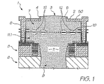
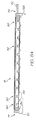
図1〜4を参照すると、本発明の一実施形態によるプリントヘッドのユニットセル1はノズル3を内部に備えたノズル板2を備え、ノズルはノズルリム4と、ノズル板の中に広がるアパーチャ5とを有する。ノズル板2は、次にエッチングされる犠牲材料の上に、化学気相成長法(CVD)を用いて、堆積された窒化ケイ素構造体からプラズマエッチングされる。
1-4 and Description of General Operation Referring to FIGS. 1 to 4, a
プリントヘッドは、また、各ノズル3に関して、ノズル板が担持される側壁6と、壁及びノズル板2によって画成されるチャンバ7と、多層基板8と、多層基板の中を通り基板の裏側(図示せず)まで延びる入口通路9とを含む。ループ状の細長いヒーター素子10はチャンバ7内に吊り下げられるので、素子は吊り梁の形である。図示されるようなプリントヘッドは、微小電気機械システム(MEMS)構造体であり、以下で詳述されるリソグラフィックプロセスによって形成される。
The print head also includes, for each
プリントヘッドが使用されているとき、インク11は貯蔵庫(図示せず)から入口通路9を介してチャンバ7へ入るので、チャンバは図1に示されたレベルまで充填される。次に、ヒーター素子10が1マイクロ秒よりも多少短い時間に亘って加熱され、その加熱は熱パルスの形式である。ヒーター素子10はチャンバ7内のインク11と熱接触するので、素子が加熱されるとき、インク内に気泡12を発生させることがわかる。したがって、インク11は泡形成液体の構成要素である。図1は、熱パルス発生の約1ミリ秒後における、すなわち、ちょうど泡がヒーター素子10上に凝集されたときの泡12の形成を示す。熱はパルスの形で加えられるので、泡12を発生させるために必要な全エネルギーは短時間のうちに供給されるべきであることがわかる。
When the print head is in use, the
図34を簡単に参照すると、以下で詳述されるように、リソグラフィックプロセス中に、プリントヘッドのヒーター14(このヒーターは上記の素子10を含む)を形成するマスク13が示されている。マスク13はヒーター14を形成するため使用されるので、その様々な部分の形状は素子10の形状に対応する。マスク13は、したがって、ヒーター14の様々な部分を識別するために役立つ基準を提供する。ヒーター14は、マスク13の15.34で指定される部分に対応する電極15と、マスクの10.34で指定される部分に対応するヒーター素子10とを有する。動作中に、電圧が電極15の両端間に印加され、素子10に電流を通す。電極15は素子10よりも遙かに厚いので、電気抵抗の大部分は素子によって与えられる。したがって、ヒーター14を動かす際に消費される殆どすべての電力は素子10によって散逸され、上記の熱パルスを生ずる。
Referring briefly to FIG. 34, as will be described in detail below, there is shown a
素子10が上記のように加熱されるとき、泡12は素子の全長に沿って作られ、この泡は、図1の断面図では、断面図に示された素子部分のそれぞれに1個ずつの4個の泡部分として示されている。
When the
泡12は、一旦発生させられると、チャンバ7内の圧力を増加させ、この圧力増加は次にノズル3を通してインク11の液滴16を射出させる。リム4は、液滴16が射出されたときに液滴を方向付けるので、液滴の方向の誤りの危険を最小限に抑える。
Once generated, the
入口通路9ごとに1台のノズル3と1台のチャンバ7しか存在しない理由は、チャンバ内で発生される圧力波が、素子10の加熱時及び泡12の形成時に、隣接するチャンバ及びそれらの対応するノズルに影響を与えないようにするためである。
There is only one
ヒーター素子10が固体材料に埋め込まれるのではなく吊されることの利点は後述される。
The advantages of the
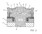
図2及び3は、後の連続した2段階のプリントヘッドの動作時のユニットセル1を示す。泡12がさらに発生し、したがって、成長し、その結果として、インク11がノズル3を通って前進していることがわかる。図3に示されるように、成長したときの泡12の形状は、インク11の慣性力学と表面張力の組み合わせによって決まる。帳面張力は泡12の表面積を最小化する傾向があるので、ある程度の量の液体が気化されるときまで、泡は基本的に円板状である。
2 and 3 show the
チャンバ7内の圧力増加は、インク11をノズル3から押し出すだけでなく、一部のインクを入口通路9から押し戻す。しかし、入口通路9は長さが約200〜300ミクロンであり、直径が約16ミクロンしかない。したがって、かなりの粘性抵抗がある。その結果、チャンバ7内の圧力増加の圧倒的な影響は、インクを射出された液滴としてノズル3を通して押し出すことであり、入口通路9を通して押し戻すことではない。
The pressure increase in the
次に図4を参照すると、さらに別の連続した動作段階におけるプリントヘッドが示され、液滴が離脱する前の「ネッキングフェーズ」中の射出されているインク液滴16が示されている。この段階では、泡12は既にその最大サイズに到達し、図5にさらに詳細に示されているように、崩壊点17へ向かって壊れ始めている。
Referring now to FIG. 4, the printhead is shown in yet another successive phase of operation, showing the ejected
崩壊点17へ向かう泡12の崩壊は、崩壊点へ向かって、一部のインク11をノズル3内部から(液滴の側面18から)取り出し、一部を入口通路9から取り出す。このようにして取り出された大半のインク11はノズル3から取り出され、液滴が離脱する前に液滴16のベースに環状のネック19を形成する。
The collapse of the
液滴16は、離脱するためには、表面張力に打ち勝つためのある程度の運動量を必要とする。インク11が泡12の崩壊によってノズル3から取り出されるとき、ネック19の直径は減少するので、液滴を保持する総表面張力の量が減少し、その結果、液滴がノズルから射出されるときの液滴の運動量は液滴を離脱させることが十分に可能である。
In order to detach, the
液滴16が離脱するとき、泡12が崩壊点17まで崩壊するので、矢印20によって示されるようなキャビテーション力が生じる。なお、崩壊点17の近傍には、キャビテーションが影響する可能性のある固体表面が存在しないことに注意する必要がある。
When the
製造プロセス
本発明の一実施形態によるプリントヘッドの製造プロセスの関連部分が図6〜29を参照して説明される。
Manufacturing Process Relevant portions of the printhead manufacturing process according to one embodiment of the present invention will be described with reference to FIGS.
図6を参照すると、Memjetプリントヘッドの一部であり、製造プロセスの中間段階におけるシリコン基板部21を通る断面図が示されている。同図はユニットセル1に対応するプリントヘッドの一部に関係する。以下の製造プロセスの説明はユニットセル1についての説明であるが、このプロセスはプリントヘッド全体を構成する多数の隣接ユニットセルに適用されることが理解される。
Referring to FIG. 6, there is shown a cross-sectional view through the
図6は、製造プロセス中であって、基板部21内の領域22におけるCMOS駆動トランジスタ(図示せず)の製作を含む標準的なCMOS製作プロセスの終了後であり、かつ、標準的なCMOS相互接続層23及びパッシベーション層24の完了後における、次の連続的なステップを示す。破線25で示された配線は、トランジスタとその他の駆動回路(同様に図示せず)とノズルに対応したヒーター素子とを電気的に相互接続する。
FIG. 6 is during the manufacturing process, after the completion of a standard CMOS fabrication process, including fabrication of a CMOS drive transistor (not shown) in
保護リング26は、インク11が、ユニットセル1のノズルが形成される27で示された領域から基板部21を介して配線25を含む領域まで拡散し、22で示された領域に配置されたCMOS回路を腐食することを防止するため、相互接続層23のメタライゼーションに形成される。
The
CMOS製作プロセスの終了後の最初の段階は、パッシベーション凹部29を形成するためにパッシベーション層24の一部をエッチングする。
The first step after the CMOS fabrication process is to etch a portion of the
図8は、相互接続層23のエッチング後に、開口部30を形成するための製造段階を示す。開口部30は、プロセスのもっと後で形成されるチャンバへのインク入口通路を構成する。
FIG. 8 shows a manufacturing stage for forming the
図10は、ノズルが形成されるべき場所で基板部21に孔31をエッチングした後の製造段階を示す。製造プロセスのもっと後で、さらなる孔(破線32で示される)が孔31とつながるように基板部21の反対側(図示せず)からエッチングされ、チャンバまでの入口通路を完成する。このように、孔32は、遠く離れた基板部の反対側から相互接続層23のレベルまでエッチングする必要がない。
FIG. 10 shows the manufacturing stage after etching the
逆に、孔32が遠方から相互接続層23までエッチングされなければならないならば、孔32が領域22内のトランジスタを破壊するまでエッチングされることを回避するため、孔32は、エッチングの不正確さに対する適切な余白(矢印34によって示される)を残すため、その領域からより遠い距離でエッチングされるべきである。しかし、基板部21の上端からの孔31のエッチングと、これにより短縮された孔32の奥行きは、残されるべき余白34をより小さくできること、及びノズルのパッキング密度を実質的に増加させ得ることを意味する。
Conversely, if the
図11は4ミクロンの厚さの犠牲レジストの層35が層24に堆積した後の製造段階を示す。この層35は孔31を埋め、プリントヘッドの構造体の一部を形成する。レジスト層35は、凹部36及び溝部37を形成するため、(図12に示されたマスクによって表現されるような)ある種のパターンで露光される。これにより、製造プロセスの後の段階で形成されるヒーター素子の電極15のための接点が作られる。溝部37は、プロセスの後の段階で、チャンバ7の一部を画成するノズル壁6を作る。
FIG. 11 shows the manufacturing stage after a 4 micron thick layer of sacrificial resist 35 has been deposited on
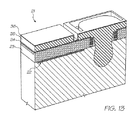
図13は、本実施形態では窒化チタンで作られた0.25ミクロンの厚さのヒーター材料の層38を層35に堆積させた後の製造段階を示す。
FIG. 13 shows the manufacturing stage after depositing on layer 35 a
図14は、ヒーター素子10及び電極15を含むヒーター14を形成するため、ヒーター層38をパターニングしエッチングした後の製造段階を示す。
FIG. 14 shows the manufacturing stage after the
図16は、約1ミクロンの厚さの別の犠牲レジスト層39が加えられた後の製造段階を示す。
FIG. 16 shows the manufacturing stage after another sacrificial resist
図18は、第2のヒーター材料の層40が堆積した後の製造段階を示す。好ましい一実施形態において、この層40は、第1のヒーター層38と同様に、0.25ミクロンの厚さの窒化チタンで作られる。
FIG. 18 shows the manufacturing stage after the second
図19は、参照番号41によって示された図のようなパターンを形成するためにエッチングされた後の第2のヒーター材料の層40を示す。この説明図において、パターン付きの層はヒーター層素子10を含まず、この意味において、ヒーター機能性をもたない。しかし、このヒーター材料の層は、ヒーター14の電極15の抵抗を低下させるために役立つので、動作中に、電極によって消費されるエネルギーが減少し、ヒーター素子10はより大量のエネルギー消費が可能になり、したがって、ヒーター素子10の効果を高めることが可能である。図38に示された二重ヒーターの実施形態において、対応する層40はヒーター14を収容する。
FIG. 19 shows the
図21は、犠牲レジストからなる第3の層42が堆積した後の製造段階を示す。この層の最上レベルは後で形成されるべきノズル板2の内側表面、したがって、ノズルアパーチャ5の内側範囲を構成するので、この層42の高さは、プリントヘッドの動作中に、43で示された領域内に泡12を形成することを可能にさせるために十分でなければならない。
FIG. 21 shows the manufacturing stage after the
図23は、最上層44、すなわち、ノズル板2を構成する層が堆積した後の製造段階を示す。100ミクロンの厚さのポリイミド膜から形成されるのではなく、ノズル板2はわずか2ミクロンの厚さの窒化ケイ素から形成される。
FIG. 23 shows the manufacturing stage after the
図24は、ノズルリム4の外側部分を形成するように、層44を形成する窒化ケイ素の化学気相成長(CVD)が45で示された場所で部分的にエッチングされた後の製造段階を示し、この外側部分は41で示されている。
FIG. 24 shows the manufacturing stage after the chemical vapor deposition (CVD) of silicon
図26は、ノズルリム4の形成を完了し、ノズルアパーチャ5を形成するために窒化ケイ素のCVDが46を通して幅広くエッチングされ、かつ、CVD窒化ケイ素が必要とされない47で示される場所で除去された後の製造段階を示す。
FIG. 26 shows that after the formation of the
図28はレジストの保護層48が塗布された後の製造段階を示す。この段階の後、基板部21は、基板部をその公称厚の約800ミクロンから約200ミクロンまで縮小し、次に、上記のように孔32をエッチングするため、その反対側(図示せず)から研磨される。孔32は、それが孔31に達するような深さまでエッチングされる。
FIG. 28 shows the manufacturing stage after the resist protective layer 48 has been applied. After this stage, the
次に、レジスト層35、39、42及び48のそれぞれの犠牲レジスタが、一体的にチャンバ7を画成する壁6及びノズル板2を備えた(壁及びノズル板の一部が切り取られて図に示されている)図30に示されるような構造体を形成するため、酸素プラズマを使用して除去される。なお、これは、孔31を埋めるレジストを取り除くためにも役立つことに注意する必要があり、この孔は、孔32(図30に示されない)と一体となって、基板部21の下方側からノズル3へ延びる通路を画成し、この通路がチャンバ7へ至る全体的に9で示されたインク入口通路としての役割を果たす。
Next, each of the sacrificial resistors of the resist
上記の製造プロセスは図30に示されたプリントヘッドの実施形態を製造するため使用されるが、様々なヒーター構造体を有するさらなるプリントヘッドの実施形態が図33、図35及び37、並びに図38及び40に示されている。 Although the above manufacturing process is used to manufacture the printhead embodiment shown in FIG. 30, additional printhead embodiments with various heater structures are shown in FIGS. 33, 35 and 37, and FIG. And 40.
インク液滴射出の制御
図30を再参照すると、上記のような図示されたユニットセル1は、壁6とノズル板2の一部が切り取られ、チャンバ7の内部が示されている。図示されたヒーター14は切り取られていないので、ヒーター素子10の両方の半分が見える。
Control of Ink Droplet Ejection Referring again to FIG. 30, the
動作中に、インク11はインク入口通路9(図28を参照)を通り、チャンバ7を満たす。次に、電圧が電極15の両端間に印加され、ヒーター素子10を通る電流の流れを定める。これは、図1に関して説明したように素子10を加熱し、チャンバ7内のインクに気泡を形成する。
During operation,
ヒーター14について考えられる様々な構造体は、そのうちの一部が図33、35、37及び38に示されているが、ヒーター素子10の長さと幅の比率に多様な変化を与えることが可能である。このような変化は(たとえ、素子10の表面積が同じであるとしても)、素子の電気抵抗に、したがって、素子のある種の電力を実現するための電圧と電流の間のバランスに重大な影響がある。
A variety of possible structures for the
最新型の駆動電子コンポーネントは、従来型よりも所要の駆動電力が小さく、「オン」状態の駆動トランジスタの抵抗が小さいという傾向がある。したがって、このような駆動トランジスタにおいて、一定のトランジスタ面積に対して、各プロセス内の電流能力が増加し、電圧許容値が低下する傾向がある。 State-of-the-art drive electronic components tend to require less drive power than conventional types, and the resistance of drive transistors in the “on” state is low. Therefore, in such a drive transistor, the current capability in each process tends to increase and the allowable voltage value tends to decrease for a certain transistor area.
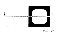
上記の図36は、図35に示されたプリントヘッドの実施形態のヒーター構造体を形成するマスクの形状を平面図で示す。したがって、図36はその実施形態のヒーター素子10の形状を表現するので、ヒーター素子を説明する際に参照される。動作中に、電流は電極15へ垂直に流れるので(15.36で示された部分によって示される)、電極の電流フロー面積はかなり広く、その結果として、電気抵抗が小さくなる。これに対して、10.36によって示された部分により図36に表現されている素子10は、長く、かつ、薄く、本実施形態の素子の幅は1ミクロンであり、厚さは0.25ミクロンである。
FIG. 36 above shows in plan view the shape of the mask that forms the heater structure of the printhead embodiment shown in FIG. Therefore, FIG. 36 represents the shape of the
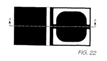
図33に示されたヒーター14は図35に示された素子10よりも著しく小さい素子10を有し、単一のループ36しか持たないことに注意すべきである。したがって、図33の素子10は、図35の素子10よりも非常に小さい電気抵抗を有し、かつ、より大きい電流の流れを許容する。その結果として、所定のエネルギーを所定の時間内にヒーター14へ送るために要する駆動電力が小さい。
It should be noted that the
図38では、これに対して、図示された実施形態は、同じユニットセル1に対応する2台のヒーター素子10.1及び10.2を有するヒーター14を含む。これらの素子の一方10.2はもう一方の素子10.1の2倍の幅があり、それに応じて表面積が広い。下方の素子10.2の様々なパスは幅が2ミクロンであり、上方の素子10.1の様々なパスは幅が1ミクロンである。したがって、下方の素子10.2によってチャンバ7内のインクに印加されるエネルギーは、所定の駆動電力及びパルス間隔で上方の素子10.1によって印加されるエネルギーの2倍である。これは、気泡のサイズ、したがって、泡によって射出されるインク液滴のサイズの調整を可能にする。
In contrast, in FIG. 38, the illustrated embodiment includes a
上方の素子10.1によってインクに印加されるエネルギーがXであると仮定すると、下方の素子10.2によって印加されるエネルギーは約2Xであり、2台の素子が一体となって印加するエネルギーは約3Xであることがわかる。勿論、どちらの素子も動作していないときに印加されるエネルギーはゼロである。したがって、実際上、2ビットの情報が1台のノズル3を用いて印刷される。
Assuming that the energy applied to the ink by the upper element 10.1 is X, the energy applied by the lower element 10.2 is about 2X, and the energy applied by the two elements together. Is about 3X. Of course, the energy applied when neither element is operating is zero. Therefore, in practice, 2-bit information is printed using one
上記のエネルギー出力の倍率は実際には正確に達成されないので、素子10.1及び10.2の正確なサイジング、又はそれらの素子に印加される駆動電圧のある程度の「微調整」が必要である。 Since the magnification of the above energy output is not actually achieved accurately, precise sizing of elements 10.1 and 10.2, or some “fine tuning” of the drive voltage applied to those elements is required. .
同様に、上方の素子10.1は下方の素子10.2に対して垂直軸の周りに180°回転させられることに注意すべきである。このため、それらの電極15は一致せず、別個の駆動回路へ独立に接続することが可能である。
Similarly, it should be noted that the upper element 10.1 is rotated 180 ° about the vertical axis relative to the lower element 10.2. For this reason, the
特定の実施形態の特徴及び効果
以下では、適切な見出しの下に、本発明の実施形態のある種の具体的な特徴とこれらの特徴の効果が検討される。これらの特徴は、コンテキストがある種の図面を特に除外し、特に言及された図面に関係しない限り、本発明に属する図面のすべてに関連して考慮されるべきである。
Features and Effects of Certain Embodiments In the following, certain specific features of embodiments of the present invention and the effects of these features are discussed under appropriate headings. These features should be considered in connection with all of the drawings belonging to the present invention unless the context specifically excludes certain types of drawings and not specifically related to the referenced drawings.
吊り梁ヒーター
図1を参照すると、既に記載したように、ヒーター素子10は吊り梁の形であり、インク11(泡形成液体)の少なくとも一部分(11.1で示される)の上に吊される。素子10はこのようにして構成され、Hewlett Packard(ヒューレットパッカード)、Canon(キャノン)、及びLexmarkレックスマークのような様々な製造業者によって作られた既存のプリントヘッドシステムにおける場合のように、基板の一部を形成し、又は基板に埋め込まれるのではない。これは本発明の実施形態と従来のインクジェットテクノロジーとの間の重大な差異となる。
Suspension Heater Referring to FIG. 1, as already described, the
この特徴の主要な効果は、従来技術の装置において行われる、ヒーター素子10を取り囲む不必要な固体材料(例えば、チャンバ壁6を形成し、入口通路9を取り囲む固体材料)の加熱を回避することによって、より高い効率が達成されることである。このような固体材料の加熱は気泡12の形成に寄与しないので、このような材料の加熱はエネルギーの浪費を伴う。泡12の発生に有意に寄与する唯一のエネルギーは、加熱されるべき液体に直接加えられるエネルギーであり、この液体は典型的にインク11である。
The main effect of this feature is to avoid heating of unnecessary solid material surrounding the heater element 10 (eg, the solid material forming the
好ましい一実施形態では、図1に示されるように、ヒーター素子10はインク11(泡形成液体)内に吊されるので、この液体は素子を取り囲む。これはさらに図41に示されている。別の可能な実施形態では、図42に示されるように、ヒーター素子10のビームはインク(泡形成液体)11の表面で吊されるので、この液体は、素子を取り囲むのではなく、素子よりも下だけに存在し、素子の上方側には空気が存在する。図41に関して記載された実施形態は、泡が素子よりも下だけに形成される図42に関して記載された実施形態とは異なり、泡12が素子10の周囲全体に形成されるので好ましい。したがって、図41の実施形態は、より効率的な動作を提供する可能性が高い。
In a preferred embodiment, as shown in FIG. 1, the
例えば、図30及び31を参照してわかるように、ヒーター素子10のビームは片側だけで支持され、その反対側では自由にされているので、このビームは片持ち梁を構成する。
For example, as can be seen with reference to FIGS. 30 and 31, the beam of the
プリントヘッドの効率
今検討中の特徴は、インク11に泡12を形成し、ノズル3を通してインク液滴16を射出するため十分に素子を加熱するために素子に印加する必要があるエネルギーが500ナノジュール(nJ)未満であるように、ヒーター素子10が構成されることである。好ましい一実施形態において、所要エネルギーは300nJ未満であり、さらなる一実施形態では、エネルギーは120nJ未満である。
Printhead Efficiency The feature under consideration is that the energy required to be applied to the element to form a
当業者に認められるように、従来技術の装置は一般に、気泡12を発生させてインク液滴16を射出するため十分に素子を加熱するためには5マイクロジュール以上を必要とする。したがって、本発明の所要エネルギーは従来のサーマルインクジェットシステムの所要エネルギーよりもオーダーが1桁少ない。この消費エネルギーの削減は、動作コストの削減、電源の小型化などを可能にするが、また、プリントヘッド冷却を大幅に簡単化し、ノズル3の高密度化を可能にし、より高解像度での印刷を可能にする。
As will be appreciated by those skilled in the art, prior art devices generally require more than 5 microjoules to heat the element sufficiently to generate
これらの本発明の効果は、以下で詳述されるように、個々の射出されたインク液滴16がそれ自体でプリントヘッドの主要な冷却機構となる実施形態において特に重要である。
These inventive effects are particularly important in embodiments where individual ejected
プリントヘッドの自己冷却
本発明のこの特徴によれば、気泡12を形成してインク11の液滴16を射出するためにヒーター素子10に印加されたエネルギーは、射出された液滴自体によって除去されたエネルギーと、インク貯蔵室(図示せず)からプリントヘッドへ取り込まれたインクとの組み合わせによって、プリントヘッドから除去される。この結果として、熱の正味の「移動」はプリントヘッドから外向きであり、自動冷却を提供する。これらの状況下で、プリントヘッドはその他の冷却システムを必要としない。
Printhead Self-Cooling According to this aspect of the invention, the energy applied to the
射出されたインク液滴16と、射出された液滴を補充するためプリントヘッドに引き込まれるインク11の量は、同じタイプの液体によって構成され、基本的に同じ質量からなるので、エネルギーの正味の移動を、一方で、素子10の加熱によって加えられたエネルギーとして、他方で、インク液滴16の射出とインク11の補充量の取り入れとから生じる熱エネルギーの正味の除去として表現すると都合がよい。インク11の補充量が周囲温度であると仮定すると、射出されたインクとインクの補充量の正味の移動によるエネルギーの変化は、射出される液滴16の温度を、もしその温度が周囲温度であるならば、液滴が射出されるときの実際の温度まで上昇させるために必要となる熱として表現できるので都合がよい。
The amount of
上記の規準が満たされるかどうかの判定は、何が周囲温度を構成するかということに依存することがわかる。本例では、周囲温度であると見なされる温度は、インク11がプリントヘッドの入口通路9に流体連通状態で接続されたインク貯蔵庫(図示せず)からプリントヘッドへ入るときの温度である。典型的に、周囲温度は、通常およそ20℃(摂氏)である室温である。
It can be seen that the determination of whether the above criteria are met depends on what constitutes the ambient temperature. In this example, the temperature considered to be the ambient temperature is the temperature at which the
しかし、周囲温度は、例えば、室温がより低いならば、又はプリントヘッドへ入るインク11が冷却されているならば、もっと低くてもよい。
However, the ambient temperature may be much lower, for example if the room temperature is lower or if the
好ましい一実施形態において、プリントヘッドは、完全な自己冷却を実現するように設計される(すなわち、インク11の射出と補充の正味の影響による放熱エネルギーはヒーター素子10によって加えられる熱エネルギーに一致する。)。
In a preferred embodiment, the print head is designed to achieve complete self-cooling (ie, the heat dissipated energy due to the net effect of
一例として、インク11が泡形成液体であり、水性であり、したがって、約100℃の沸点を有すると仮定し、周囲温度が40℃であるならば、周囲温度からインク沸点温度までの最大値は60℃であり、これはプリントヘッドに起こり得る最大温度上昇である。
As an example, assuming that
プリントヘッド内のインク温度が(インク液滴16の射出以外のときに)インク11の沸点に非常に近づくことは避ける方が望ましい。インク11がこのような温度になると、プリントヘッドの部品間の温度変化によって一部の領域が予期せずに沸点よりも高くなり、その結果として、好ましくない気泡12の形成を生ずることがある。したがって、本発明の好ましい一実施形態は、加熱素子10が動作していないときに特定のノズルチャンバ7内のインク11(泡形成液体)の最高温度がその沸点よりも10℃低くなるとき、上記のような完全な自己冷却が実現されるよう構成される。
It is desirable to avoid that the ink temperature in the print head is very close to the boiling point of the ink 11 (other than when the
現在検討中の特徴及びその様々な実施形態の主要な効果は、インク液滴16が射出されているノズルに隣接するノズル3の望ましくない沸騰を防止する複雑な冷却方法を必要とすることなく、高いノイズ密度と高速プリントヘッド動作を可能にすることである。これは、このような特徴及び上記の温度規準が存在しない場合よりもノズルパッキング密度を100倍程度増加させることが可能である。
The features currently under consideration and the main effects of the various embodiments thereof, without the need for complex cooling methods to prevent undesired boiling of the
ノズルの面積密度
本発明のこの特徴は、プリントヘッドのノズル3の単位面積当たりの密度に関係する。図1を参照すると、ノズル板2は上側表面50を有し、本発明のこの態様はその表面上のノズル3のパッキング密度に関係する。より詳細には、その表面50上のノズル3の面積密度は、表面積1平方cm当たりのノズル数が10000台以上である。
Nozzle Area Density This feature of the present invention relates to the density per unit area of the
好ましい一実施形態において、面積密度は表面50の面積の1平方cm当たりのノズル3の数が20000台以上であり、別の好ましい実施形態では、面積密度は1平方cm当たりのノズル3の数が40000台以上である。好ましい実施形態では、面積密度は1平方cm当たりのノズル3の数が48828台である。
In a preferred embodiment, the area density is 20,000 or
面積密度について言及すると、各ノズル3は、典型的に、駆動トランジスタ、シフトレジスタ、イネーブルゲート、及びクロック再生回路(この回路は具体的に識別されていない)により構成された、ノズルに対応する駆動回路を含むものと考えられる。
Referring to area density, each
単一のユニットセル1が示された図43を参照すると、ユニットセルの寸法は、幅が32ミクロン、長さが64ミクロンとして示されている。次の連続するノズル行(図示せず)のノズル3は、このノズルのすぐ隣りに並列するので、プリントヘッドチップの外周の寸法の結果として、1平方cm当たりに48828台のノズル3が存在する。これは、典型的なサーマルインクジェットプリントヘッドのノズル面積密度の約85倍であり、ピエゾプリントヘッドのノズル面積密度のおよそ400倍である。
Referring to FIG. 43 where a
高面積密度の主要な効果は、装置が特定のサイズのシリコンウェハー上に一括製作されるので、製造コストが安いことである。 The main effect of high area density is low manufacturing cost because the device is fabricated in bulk on a silicon wafer of a specific size.
基板の1平方cm当たりに収容できるノズル3の台数が増加すると、より多数のノズルを、典型的に1枚のウェハーからなる1回のバッチで製作することが可能である。本発明のプリントヘッドにおいて使用されるタイプのCMOS−MEMSウェハーを製造するコストは、ある程度まで、その上に形成されるパターンの性質に依存しない。したがって、パターンが非常に小さいならば、非常に多数のノズル3を収容することが可能である。このため、ノズルがより低い面積密度を有する場合よりも多数のノズル3及び多数のプリントヘッドを同じコストで製造できる。コストはノズル3が占める面積に正比例する。
As the number of
ヒーター素子の反対側での泡形成
この特徴によれば、ヒーター14は、泡12がインク11(泡形成液体)内で形成されるときに、泡がヒーター素子10の両側に形成されるように構成される。好ましくは、泡は、ヒーター素子10が吊り梁の形であるならば、ヒーター素子10を取り囲むように形成される。
Foam formation on the opposite side of the heater element According to this feature, the
泡12をヒーター素子10の一方側だけでなく、両側に形成することは、図45及び46を参照して理解できる。これらのうちの最初の図において、ヒーター素子10は、泡12を一方側だけに形成するため適合し、一方、2番目の図において、素子は泡12を両側に形成するため適合していることが示されている。
It can be understood with reference to FIGS. 45 and 46 that the
図45のような構成において、泡12がヒーター素子10の一方側だけに形成される理由は、素子が基板51に埋め込まれ、その結果、泡が基板に対応した特定の側面に形成され得ないからである。これに対して、泡12は、図46の構造では、ヒーター素子10が吊されているので、両側に形成される。
In the configuration as shown in FIG. 45, the reason why the
勿論、ヒーター素子10が図1に関して説明したように吊り梁の形である場合、泡12は吊り梁素子を取り囲むように形成することが可能である。
Of course, if the
泡12が両側に形成されることの効果は、より高い効率が達成できることである。これは、ヒーター素子10の付近において加熱固体材料内で浪費され、泡12の形成に寄与しない熱が減少するためである。これは図45に示され、矢印52は熱の固体基板51への移動を示す。基板51の方へ損出される熱の量は、水性であるインク11の熱伝導率に対する基板の固体材料の熱伝導率に依存する。水の熱伝導率はかなり低いので、熱の半分以上がインク11ではなく基板51によって吸収されることが予測される。
The effect of the
キャビテーションの防止
上記のように、泡12が本発明の一実施形態によるプリントヘッド内に形成された後、泡は崩壊点17へ向かって壊れる。ここで取り扱われる特徴によれば、ヒーター素子10は、泡12を形成し、泡が崩壊するときに向かう崩壊点17はヒーター素子から離れた位置であるように構成される。好ましくは、プリントヘッドは、このような崩壊点17に固体材料が存在しないように構成される。このようにして、従来技術のサーマルインクジェット装置において重大な問題であるキャビテーションは大部分が取り除かれる。
Preventing Cavitation As described above, after the
図48を参照すると、好ましい一実施形態において、ヒーター素子10は、ギャップ(矢印54によって示される)を画成する部品53を有し、泡12を形成し、その泡が壊れる崩壊点17がそのギャップに位置するように構成される。この特徴の効果は、ヒーター素子10及びその他の固体材料に対するキャビテーションダメージを実質的に回避することである。
Referring to FIG. 48, in a preferred embodiment, the
図47に概略的に示されるような標準的な従来技術のシステムにおいて、ヒーター素子10は基板55に埋め込まれ、絶縁層56がその素子を覆い、保護層57が絶縁層を覆う。泡12が素子10によって形成されるとき、泡は素子の最上部に形成される。泡12が壊れるとき、矢印58によって示されるように、泡崩壊のすべてのエネルギーが非常に小さい崩壊点17に集中する。保護層57が無い場合、崩壊点17へのこのエネルギーの集中から生ずるキャビテーションを原因とする機械力がヒーター素子10を崩すか、若しくは、破壊する。しかし、これは保護層57によって防止される。
In a standard prior art system as schematically shown in FIG. 47, the
典型的に、このような保護層57はタンタルから作られ、酸化して非常に硬い5酸化タンタル(Ta2O5)の層を形成する。キャビテーションの効果を完全に阻害する材料は知られていないが、5酸化タンタルがキャビテーションのため崩されるならば、酸化が下にあるタンタル金属で再び起こり、5酸化タンタル層を効果的に修復する。 Typically, such a protective layer 57 is made of tantalum and oxidizes to form a very hard layer of tantalum pentoxide (Ta 2 O 5 ). No material is known that completely inhibits the effects of cavitation, but if tantalum pentoxide is destroyed due to cavitation, oxidation will occur again with the underlying tantalum metal, effectively repairing the tantalum pentoxide layer.
5酸化タンタルはこの点に関して従来のサーマルインクジェットシステムにおいて非常に巧く機能するが、ある種の欠点を有する。1つの重大な欠点は、実際において、必要なエネルギーをインク11に移動させ、泡12を形成するように加熱するため、実質的に(参照番号59によって示された厚さを有する)保護層57の全体を加熱しなければならないことである。この層57は、タンタルの原子量が非常に大きいため高熱質量を有し、これが熱移動の効率を低下させる。これは、インク11を十分に加熱するため69で示されたレベルの温度を上昇させるために59で示されたレベルで要求される熱量を増加させるだけでなく、矢印61で示された方向に実質的な熱損失を生じさせる。これらの欠点は、ヒーター素子10が表面に支えられるだけで、保護層57によって覆われていない場合には現れない。
Although tantalum pentoxide functions very well in this regard in conventional thermal ink jet systems, it has certain drawbacks. One significant drawback is that, in practice, the necessary energy is transferred to the
ここで検討中の特徴によれば、上記の保護層57の必要性は、図48に示されるように、固体材料が存在しない場所、より具体的には、ヒーター素子10の部品53の間にギャップ54が存在する場所である崩壊点17へ向かって崩壊する泡12を発生させることにより回避される。インク11自体だけが(泡発生前に)この位置にあるので、キャビテーションの効果によってここで破壊される材料は存在しない。崩壊点17における温度は、ソノルミネセンスの現象によって実証されるように、数千℃に達することがある。これは、その点におけるインク成分を破壊する。しかし、崩壊点17における極端な温度の体積は小さいので、この体積内のインク成分の破壊は僅かである。
According to the features under consideration here, the need for the protective layer 57 is shown in FIG. 48 where there is no solid material, more specifically between the
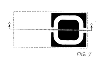
固体材料が存在しない崩壊点17へ向かって壊れるような泡12の発生は、図34に示されたマスクの部分10.34によって示された部分に対応するヒーター素子10を使用して実現される。表示された素子は対称であり、その中心に参照番号63によって示された孔を有する。その素子が加熱されるとき、泡は(破線64によって示されるように)素子の周りに形成され、次に、破線64及び65によって示されるような環状(ドーナツ型)形状ではなく、孔63を有する素子に架かるように成長し、その孔は泡を形成する蒸気で満たされる。泡12は、したがって、実質的に円板形状である。泡が壊れるとき、この崩壊は泡12を取り囲む表面張力を最小限に抑えるように向けられる。これは、関連した力学によって許される限り球形状へ向かって動く泡形状に関連する。この結果、崩壊点はヒーター素子10の中心の孔63の領域内に収まり、そこに固体材料は存在しない。
The generation of a
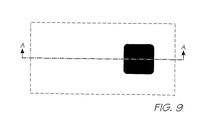
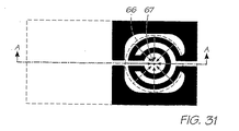
図31に示されたマスクの部分10.31によって示されたヒーター素子10は、同様の結果を得るために構成され、破線66によって示されるような泡が発生し、泡が壊れる崩壊点はその素子の中心の孔67の中にある。
The
図36に示されたマスクの部分10.36として示されたヒーター素子10もまた同じ結果を得るように構成される。素子10.36は孔68が小さくなるように寸法を決められ、ヒーター素子の製造の不正確さは、泡の崩壊点が孔によって画成される領域内に収まるように泡が形成され得る程度に影響を与える。例えば、孔は数ミクロン径と同じくらいに小さい。素子10.36において高い精度レベルが達成できないとき、これは、多少偏りのある12.36として示された泡を生ずるので、泡はこのような小領域内の崩壊点の方へ向けられない。このような場合、図36に示されたヒーター素子に関して、素子の中心ループは省くことが可能であり、これにより、泡の崩壊点が収まる領域のサイズが増加する。
The
化学気相成長法によるノズル板と薄いノズル板
各ユニットセル1のノズルアパーチャ5はノズル板2を貫通し、ノズル板は、このようにして、化学気相成長法(CVD)により形成された構造体を構成する。様々な好ましい実施形態において、CVDは窒化ケイ素、二酸化ケイ素、又はオキシナイトライドである。
Nozzle plate and thin nozzle plate by chemical vapor deposition method The
CVDによって形成されたノズル板2の効果は、ノズル板がそれをユニットセル1の壁6のような他の部品に組み付けることを必要とせずに定位置に形成されることである。これは重要な効果であり、その理由は、さもなければ必要になるノズル板2の組立は、実施が困難であり、潜在的に複雑な問題を伴う可能性があるからである。このような問題は、ノズル板2とそれが組み付けられる部品との間の熱膨張が一致しない可能性、ノズル板2を他の部品に接着する接着剤の硬化過程中に、部品を互いに位置合わせした状態に保つこと、部品を平面的に保つことに成功することの困難さなどを含む。
The effect of the
熱膨張の問題は、従来技術では、製造可能であるインクジェットのサイズを制限する重要な要因である。なぜならば、例えば、基板がシリコンで作られる場合に、ニッケルのノズル板と、ノズル板が接続される基板との間の熱膨張率の差がかなり大きいからである。その結果として、例えば、1000台のノズルによって占有されるような短い距離に亘って、周囲温度から部品を一体的に接着するため必要な硬化温度まで加熱されるそれぞれの部品間に生じる相対的な熱膨張は、ノズルの全長よりも遙かに大きい寸法の不一致を引き起こす可能性がある。これはこのような装置では著しく不利である。 The problem of thermal expansion is an important factor that limits the size of ink jets that can be produced in the prior art. This is because, for example, when the substrate is made of silicon, the difference in coefficient of thermal expansion between the nickel nozzle plate and the substrate to which the nozzle plate is connected is quite large. As a result, for example, relative distances that occur between each part heated over a short distance such as occupied by 1000 nozzles from ambient temperature to the required curing temperature to bond the parts together. Thermal expansion can cause a dimensional mismatch much larger than the total length of the nozzle. This is a significant disadvantage with such devices.
少なくとも本発明の実施形態において、今検討している本発明の特徴により取り扱われる別の問題は、従来技術の装置では、組み立てる必要があるノズル板が一般に、相対的に高い応力の条件下でプリントヘッドの残りの部分の上に積層されることである。これは装置の破壊又は望ましくない変形を生じさせる。本発明の実施形態においてCVDによるノズル板2の堆積はこの問題を回避する。
Another problem addressed by the features of the present invention under consideration, at least in embodiments of the present invention, is that in prior art devices, the nozzle plates that need to be assembled generally print under relatively high stress conditions. To be stacked on the rest of the head. This can cause destruction or undesirable deformation of the device. In the embodiment of the present invention, deposition of the
少なくとも本発明の実施形態において、本発明のこの特徴のさらなる効果は、既存の半導体製造プロセスとの互換性である。CVDによるノズル板2の堆積は、半導体製造のため普通に使用されるプロセスを使用して、ノズル板が通常のシリコンウェハー製造のスケールでプリントヘッドに組み込まれることを可能にする。
At least in embodiments of the present invention, a further advantage of this feature of the present invention is compatibility with existing semiconductor manufacturing processes. The deposition of the
既存のサーマルインクジェットシステム又はバブルジェットシステムは、泡発生フェーズの間に最大で100気圧までの圧力遷移が起こる。このような装置においてノズル板2がCVDによって塗布されたならば、このような圧力遷移に抵抗するためには、かなりの厚さのCVDノズル板が要求される。当業者にとって当然であるように、堆積したノズル板の厚さは以下に説明するようなある種の問題を生じる。
Existing thermal ink jet systems or bubble jet systems undergo pressure transitions up to 100 atmospheres during the foam generation phase. If the
例えば、ノズルチャンバ7内で100気圧の圧力に抵抗するために十分な窒化物の厚さは、例えば、10ミクロンである。厚いノズル板2を有する本発明によらないユニットセル1を示す図49を参照すると、このような厚さは、液滴射出に関係する問題を生じることが認められる。この場合、ノズル板2の厚さが原因となって、インク11がノズル板を通して射出されるときに、ノズル3によって加えられる流体抗力は、装置の効率に著しい損失を生じさせる。
For example, a sufficient nitride thickness to resist a pressure of 100 atmospheres in the
このような厚いノズル板2の場合に存在する別の問題は、実際のエッチングプロセスに関係する。これは、図示されるように、ノズル3が、例えば、標準的なプラズマエッチングを使用して、基板部のウェハー8に対して垂直にエッチングされることを仮定している。これは、典型的に10ミクロンを上回るレジスト69が塗布されることを必要とする。その厚さのレジスト69を露光するためには、レジストを露光するため使用されるステッパの焦点深度がかなり浅いので、所要の解像度のレベルを達成することが困難になる。当該深さのレジスト69はx線を使用して露光することが可能であるが、これはかなりコストのかかるプロセスである。
Another problem present in the case of such a
10ミクロンの厚さの窒化物の層がシリコン基板ウェハー上に堆積したDVCである場合にこのような厚いノズル板2に関して存在するさらなる問題は、厚い堆積層内の固有の応力の他に、CVD層と基板との間には熱膨張の差があるので、リソグラフィックプロセスのさらなるステップが実行できなくなる程度までウェハーが曲げられることである。したがって、(本発明とは異なる)10ミクロン程度の厚さのノズル板2の層は、可能ではあるが、不利である。
A further problem that exists with such a
図50を参照すると、本発明の一実施形態によるMemjetサーマルインク射出装置において、CVD窒化物ノズル板層2は僅かに2ミクロンの厚さである。したがって、ノズル3の中の流体抗力は格別大きくないので、損失の主要な原因ではない。
Referring to FIG. 50, in the Memjet thermal ink ejection device according to one embodiment of the present invention, the CVD nitride
さらに、このようなノズル板2においてノズル3をエッチングするために必要なエッチング時間及びレジスト厚と、基板ウェハー8上の応力は極端な数値にはならない。
Further, the etching time and resist thickness necessary for etching the
本発明におけるかなり薄いノズル板2が可能になる理由は、チャンバ7内に発生される圧力が、上記のように従来技術の装置における100気圧ではなく、約1気圧に過ぎないからである。
The reason that a fairly
多数の要因が本システムにおいて液滴16を射出するために必要な圧力遷移の著しい低下に寄与する。それらの要因には、
1.チャンバ7の小さいサイズ
2.ノズル3及びチャンバ7の正確な製造
3.低い液滴速度における液滴射出の安定性
4.ノズル3の間の非常に低い流体クロストーク及び熱クロストーク
5.泡面積に対する最適ノズルサイズ
6.薄い(2ミクロンの)ノズル3の中の低い流体抗力
7.入口9を通るインク射出を原因とする低い圧力損失
8.自己冷却動作
が含まれる。
A number of factors contribute to the significant reduction in pressure transition required to eject
1. 1. Small size of
図6〜31の点から記載されたプロセスに関して既に説明したように、2ミクロンの厚さのノズル板層2のエッチングは、2つの関連した段階を含む。このような段階の一方は、図24及び50において45によって示された領域のエッチングを含み、外側がノズルリム4になる凹部を形成する。このような段階のもう一方は、図26及び50において46によって示された領域におけるさらなるエッチングを含み、実際にノズルアパーチャ5を形成し、リム4を仕上げる。
As already described with respect to the process described in terms of FIGS. 6-31, the etching of the 2 micron thick
ノズル板厚
CVDによるノズル板2の形成に関して、その観点で記載された効果と共に説明したように、本発明におけるノズル板は従来技術よりも薄い。より詳細には、ノズル板2は10ミクロンの厚さよりも薄い。好ましい一実施形態において、各ユニットセル1のノズル板2は5ミクロンの厚さよりも薄く、別の好ましい実施形態では、それは2.5ミクロンの厚さよりも薄い。実際上、ノズル板2の好ましい厚さは2ミクロンの厚さである。
Nozzle plate thickness As described with respect to the formation of the
種々の層に形成されたヒーター素子
この特徴によれば、複数台のヒーター素子10が各ユニットセル1のチャンバ7内に配置される。図6〜31に関して説明したリソグラフィックプロセスによって形成された素子10は、それぞれの層に形成される。
Heater elements formed in various layers According to this feature, a plurality of
好ましい実施形態によれば、図38、40及び51に示されるように、チャンバ7内のヒーター素子10.1及び10.2は互いにサイズが異なる。
According to a preferred embodiment, as shown in FIGS. 38, 40 and 51, the heater elements 10.1 and 10.2 in the
また、上記のリソグラフィックプロセスの説明を参照してわかるように、各ヒーター素子10.1、10.2はそのプロセスの少なくとも1ステップによって形成され、素子10.1の1つずつに関係するリソグラフィックプロセスは他の素子10.2に関係するリソグラフィックプロセスと区別される。 Also, as can be seen with reference to the description of the lithographic process above, each heater element 10.1, 10.2 is formed by at least one step of the process and is associated with one of the elements 10.1. The graphic process is distinguished from the lithographic process associated with other elements 10.2.
素子10.1、10.2は、好ましくは、バイナリ重み付きインク液滴体積を実現できるように、すなわち、異なるバイナリ重み付き体積を有するインク液滴16が特定のユニットセル1のノズル3を通して射出させられるように、図51の図に概略的に反映されるように、相対的にサイジングされる。インク液滴16の体積に付けられるバイナリ重みは、素子10.1と10.2の相対的なサイズによって決まる。図51において、インク11に接触する底側ヒーター素子10.2の面積は上側ヒーター素子10.1の面積の2倍である。
The elements 10.1, 10.2 are preferably arranged so that binary weighted ink droplet volumes can be realized, i.e.
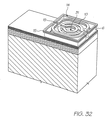
Canon(キャノン)が特許を取得し、図52に概略的に示された1つの既知の従来技術の装置は同様にノズルごとに2台のヒーター素子10.1及び10.2を有し、これらは同様にバイナリに基づいて(すなわち、バイナリ重み付き体積で液滴16を生成するため)サイジングされる。これらの素子10.1、10.2は、ノズルチャンバ7内で互いに隣接した単一の層に形成される。小さい素子10.1によって形成された泡12.1だけがかなり小さく、一方、大きい素子10.2によって形成された泡12.2だけがかなり大きいということがわかる。2台の素子の組み合わせ効果によって発生した泡は、同時に動かされるとき、12.3によって示される。3通りの異なるサイズのインク液滴16は、3個のそれぞれの泡12.1、12.2及び12.3によって射出させられる。
One known prior art device, patented by Canon and schematically shown in FIG. 52, also has two heater elements 10.1 and 10.2 per nozzle, Are similarly sized based on the binary (ie, to produce
素子10.1及び10.2自体のサイズは、異なるサイズを有する液滴16を射出させるため、又は有効な液滴の組み合わせを射出させるためにバイナリ重み付けされる必要のないことわかる。実際に、バイナリ重み付けは素子10.1、10.2自体の面積によって正確に表現されない。バイナリ重み付き液滴体積を実現するために素子10.1、10.2をサイジングする際に、泡12の発生を取り囲む流体特性、液滴動特性、液滴16が途切れたときにノズル3からチャンバ7へ引き戻される液体の量などが考慮されるべきである。したがって、素子10.1、10.2の表面積の実際の比率、又は2台のヒーターの性能は、望ましいバイナリ重み付き液滴体積を得るため実際には調整されるべきである。
It can be seen that the size of elements 10.1 and 10.2 themselves do not need to be binary weighted to fire
ヒーター素子10.1、10.2のサイズが固定され、それらの表面積の比率がしたがって固定されるとき、射出液滴16の相対的なサイズは2台の素子への電源電圧を調整することにより調整される。これは、素子10.1、10.2の動作パルスの間隔、すなわち、それらのパルス幅を調整することにより達成される。しかし、パルス幅はある一定の時間を超えることができず、その理由は、一旦、泡12が素子10.1、10.2の表面に凝集すると、その時間経過後のパルス幅は全く影響しないか、又は殆ど影響しないからである。
When the size of the heater elements 10.1, 10.2 is fixed and the ratio of their surface areas is therefore fixed, the relative size of the ejected
これに対して、ヒーター素子10.1、10.2が低熱質量であるならば、ヒーター素子を、泡12が形成され液滴16が射出される温度へ非常に高速に達するように加熱することが可能である。最大実効パルス幅は、泡凝集の開始によって、典型的に約0.5ミリ秒に制限されるが、最小パルス幅は、ヒーター素子10.1、10.2によって許容される利用可能な電流ドライブ及び電流密度だけによって制限される。
On the other hand, if the heater elements 10.1, 10.2 have a low thermal mass, the heater elements are heated so that they reach a temperature at which bubbles 12 are formed and
図51に示されるように、2台のヒーター素子10.1、10.2は2台のそれぞれの駆動回路70に接続される。これらの回路70は互いに同一でもよいが、これらの回路を用いて、例えば、上側素子10.1に接続された駆動トランジスタよりも大きく、高電流素子である下側素子10.2に接続された駆動トランジスタ(図示せず)をサイジングすることにより、さらなる調整を行うことができる。例えば、それぞれの素子10.1、10.2に供給される相対的な電流が2:1の比率であるならば、下側素子10.2に接続された回路70の駆動トランジスタは、典型的に、もう一方の素子10.1に接続された回路70の駆動トランジスタ(図示せず)の幅の2倍になる。
As shown in FIG. 51, the two heater elements 10.1, 10.2 are connected to the two
図52に関連して説明される従来技術において、同じ層にあるヒーター素子10.1、10.2は、リソグラフィック製造プロセスの同じステップにおいて同時に製作される。図51に示された本発明の実施形態では、上記の2台のヒーター素子10.1、10.2は次々に形成される。実際には、図6〜31を参照して例示されたプロセスにおいて説明されるように、素子10.2を形成する材料が堆積され、次に、リソグラフィックプロセスにおいてエッチングされ、その後、犠牲層39がその素子の最上部に堆積され、次に、もう一方の素子10.1の材料が堆積され、その結果、犠牲層が2層のヒーター素子層に挿まれる。第2の素子10.1の層は第2のリソグラフィックステップによってエッチングされ、犠牲層39が取り除かれる。
In the prior art described in connection with FIG. 52, heater elements 10.1, 10.2 in the same layer are fabricated simultaneously in the same steps of the lithographic manufacturing process. In the embodiment of the present invention shown in FIG. 51, the two heater elements 10.1, 10.2 are formed one after another. In practice, as described in the process illustrated with reference to FIGS. 6-31, the material forming element 10.2 is deposited and then etched in a lithographic process, after which
上記のように異なるサイズのヒーター素子10.1及び10.2をもう一度参照すると、これは1台のノズル3から多数のバイナリ重み付き液滴体積が得られるように素子をサイジングすることができるという効果がある。
Referring once again to the differently sized heater elements 10.1 and 10.2, as described above, it is possible to size the elements to obtain multiple binary weighted droplet volumes from a
多数の液滴体積が得られ、特に、それらがバイナリ重み付けされているならば、より少ない印刷ドット数を使用して、より低い印刷解像度で、写真のような質が得られることがわかる。 It can be seen that a large number of droplet volumes can be obtained, especially if they are binary weighted, using a lower number of printed dots and a photographic quality at a lower print resolution.
さらに、同じ状況下で、より高速な印刷が達成される。すなわち、1個だけの液滴14を射出し、次に、ノズル3が再び満たされるのを待つのではなく、1個、2個、又は3個の液滴に相当するものが射出される。ノズル3の利用可能な補充速度が制限因子ではないとするならば、最大で3倍まで高速のインク射出、したがって、印刷が達成される。しかし、実際には、ノズル補充時間は、典型的に、制限因子である。この場合、ノズル3は、(最小サイズの液滴に対して)3倍の体積の液滴16が射出されたとき、最小体積の液滴だけが射出されたときよりも僅かに長い補充時間を要する。しかし、実際には、補充するためには3倍までの時間を要しない。その原因はインク11の慣性力学及び表面張力である。
Furthermore, faster printing is achieved under the same circumstances. That is, instead of waiting for only one
図53を参照すると、一対の隣接したユニットセル1.1及び1.2が概略的に示され、左側のセル1.1はより大きい体積の液滴16が射出された後のノズル3を示し、右側のセル1.2はより小さい体積の液滴が射出された後のノズルを示す。大きい方の液滴16の場合、部分的に空になったノズル3.1の内側に形成された気泡71の曲率は、より小さい体積の液滴がもう一方のユニットセル1.2のノズル3.2から射出された後に形成された気泡72の曲率よりも大きい。
Referring to FIG. 53, a pair of adjacent unit cells 1.1 and 1.2 are schematically shown, and the left cell 1.1 shows the
ユニットセル1.1内の気泡71の曲率が大きくなると、矢印73によって示されるように、補充通路9からノズル3へ向かってチャンバ7.1内にインク11を引き込む傾向のある表面張力が大きくなる。これにより補充時間が短縮される。チャンバ7.1が補充されるとき、チャンバは、74で示される段階に到達し、その状態は隣接したユニットセル1.2内の状況と類似する。この状態において、ユニットセル1.1のチャンバ7.1は部分的に補充され、表面張力は減少している。このため、この段階において、この条件がユニットセル1.1内で達成されるときに、関連した運動量を有する液体のチャンバ7.1への流れが確立されているとしても、補充速度は低下させられる。これによる全体的な影響は、気泡71が存在するときからチャンバ7.1及びノズル3.1を完全に再充填するまでに要する時間は、状態74が存在するときからの時間よりも長くなるが、たとえ、補充されるべき体積が3倍大きい場合であっても、チャンバ7.1及びノズル3.1を補充するために要する時間は3倍も長くならないということである。
When the curvature of the
原子番号の小さい元素により構成された材料から形成されたヒーター素子
この特徴は、少なくとも重量百分率で90%が50より小さい原子番号を有する1個以上の周期元素により構成される固体材料から形成されたヒーター素子10に関連する。好ましい一実施形態において、原子量は30よりも小さく、別の実施形態では、原子量は23よりも小さい。
Heater element formed from a material composed of an element with a small atomic number This feature is formed from a solid material composed of one or more periodic elements having an atomic number of at least 90% by weight and having an atomic number of less than 50 Related to the
低原子番号の効果は、その材料の原子の質量がより小さく、したがって、ヒーター素子10の温度を上昇させるために要するエネルギーが少ないことである。その理由は、当業者によって理解されるように、物の温度は基本的に原子核の運動の状態に関連付けられているからである。したがって、軽い原子核を有する内量内よりも重い原子核を有する材料内で温度を上昇させるためには、すなわち、このような核運動を誘起するためには、より大きなエネルギーが必要である。
The effect of the low atomic number is that the mass of atoms in the material is smaller and therefore less energy is required to raise the temperature of the
サーマルインクジェットシステムのヒーター素子のため現在使用されている材料には、タンタル・アルミニウム合金(例えば、Hewlett Packard(ヒューレットパッカード)によって使用される)、及びホウ化ハフニウム(例えば、Canon(キャノン)によって使用される)が含まれる。タンタル及びハフニウムの原子番号はそれぞれ73及び72であり、一方、本発明のMemjetヒーター素子10において使用される材料は窒化チタンである。チタンの原子番号は22であり、窒素の原子番号は7であるので、これらの材料は関連した従来技術の装置材料の原子番号よりも著しく小さい。
Currently used materials for heater elements of thermal inkjet systems include tantalum aluminum alloys (eg, used by Hewlett Packard) and hafnium borides (eg, used by Canon). Included). The atomic numbers of tantalum and hafnium are 73 and 72, respectively, while the material used in the
ホウ素及びアルミニウムは、それぞれ、窒素のようにホウ化ハフニウム及びタンタル・アルミニウムのそれぞれの一部を形成し、比較的軽量の材料である。しかし、窒化タンタルの密度は16.3g/cm3であり、一方、(タンタルの代わりにチタンを含有する)窒化タンタルの密度は5.22g/cm3である。このように、窒化タンタルの密度は窒化チタンの密度の約3倍であるので、窒化チタンを加熱するために要するエネルギーは窒化タンタルのおよそ3分の1である。当業者によって理解されるように、2つの異なる温度における材料のエネルギーの差は、以下の式、
E=ΔT×CP×VOL×ρ
によって示され、ΔTは温度差を示し、Cpは比熱容量であり、VOLは体積であり、ρは材料の密度である。密度は原子番号だけでは決まらないが、密度もまた格子定数の関数であるため、密度は当該材料の原子番号による影響を強く受けるので、以下で検討する特徴の主要な様相である。
Boron and aluminum are relatively lightweight materials that form part of hafnium boride and tantalum aluminum, respectively, like nitrogen. However, the density of tantalum nitride is 16.3 g / cm 3 , while the density of tantalum nitride (containing titanium instead of tantalum) is 5.22 g / cm 3 . Thus, since the density of tantalum nitride is about three times that of titanium nitride, the energy required to heat titanium nitride is about one-third that of tantalum nitride. As will be appreciated by those skilled in the art, the difference in energy of materials at two different temperatures is given by the following equation:
E = ΔT × C P × V OL × ρ
Where ΔT is the temperature difference, C p is the specific heat capacity, V OL is the volume, and ρ is the density of the material. Although the density is not determined only by the atomic number, the density is also a function of the lattice constant, and therefore the density is strongly influenced by the atomic number of the material, and is the main aspect of the characteristics to be examined below.
低ヒーター質量
この特徴は、インク内に泡12を発生させ、インク液滴16を射出させるために、泡形成液体(すなわち、本実施形態ではインク11)の沸点よりも高く加熱される各ヒーター素子の固体材料の質量が10ナノグラム未満になるように構成されたヒーター素子10に関連する。
Low Heater Mass This feature provides each heater element that is heated above the boiling point of the foam-forming liquid (ie,
好ましい一実施形態において、質量は2ナノグラム未満であり、別の実施形態では、質量は500ピコグラム未満であり、さらに別の実施形態では、質量は250ピコグラム未満である。 In one preferred embodiment, the mass is less than 2 nanograms, in another embodiment, the mass is less than 500 picograms, and in yet another embodiment, the mass is less than 250 picograms.
上記の特徴は、ヒーター素子10の固体材料を加熱する際にエネルギー損失が減少する結果として効率を高めるので、従来技術のインクジェットシステムを上回る重要な効果を構成する。この特徴が有効になる原因は、低密度を有するヒーター素子材料の使用、素子10の比較的小さいサイズ、及び例えば、図1に示されるように、ヒーター素子が他の材料に埋め込まれない吊り梁の形をしていることである。
The above features constitute an important advantage over prior art inkjet systems because they increase efficiency as a result of reduced energy loss when heating the solid material of the
図34は図33に示されたプリントヘッドの一実施形態のヒーター構造体を形成するマスクの形状を平面図で示す。したがって、図34はその実施形態のヒーター素子10の形状を表現するので、以下でヒーター素子を検討する際に参照される。図34に参照番号10.34によって示されるようなヒーター素子は、幅が2ミクロン、かつ、厚さが0.25ミクロンである単一ループ49だけを有する。このループは、6ミクロンの外形と4ミクロンの内径を有する。ヒーター総質量は82ピコグラムである。図39において参照番号10.39によって同じように示された対応する素子10.2は質量が229.6ピコグラムであり、図36に参照番号10.36によって示された素子10は225.5ピコグラムの質量を有する。
FIG. 34 shows in plan view the shape of the mask that forms the heater structure of one embodiment of the printhead shown in FIG. Therefore, FIG. 34 represents the shape of the
例えば、図34、39及び36に示された素子10、102が使用されるとき、実際には、インクの沸点よりも高い温度まで加熱される(本実施形態では泡形成液体である)インク11と熱接触する各素子の材料の総質量は、素子が電気的絶縁性、化学的不活性、熱伝導性である材料で覆われた場合の質量よりも僅かに重い。このコーティングは、より高い温度まで上昇させられる材料の総質量をある程度まで増加させる。
For example, when the
絶縁保護コーティングされたヒーター素子
この特徴は、絶縁保護コーティングによって覆われた各素子10に関連し、このコーティングは同時に素子の全面に塗布されるので、コーティングはシームレスである。コーティング10は、好ましくは、電気的に非伝導性であり、化学的に不活性であり、高い熱伝導率を有する。好ましい一実施形態において、コーティングは窒化アルミニウムからなり、別の実施形態では、コーティングはダイヤモンド・ライク・カーボン(DLC)からなり、さらに別の実施形態では、窒化ホウ素からなる。
Insulating protective coated heater element This feature is associated with each
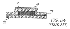
図54及び55を参照すると、上記のように絶縁保護コーティングされていないが、基板78の上に堆積され、典型的な形では、一方側が76によって示されたCVD材料によって絶縁保護コーティングされた従来技術のヒーター素子10が概略的に示される。これに対して、図56に概略的に示されるように、本例における上記のコーティングは、77によって示され、同時に全面で素子を絶縁保護コーティングする。しかし、この全面における絶縁保護コーティング77は、素子10が、コーティングされているときに、他の構造体から分離された構造体である場合、すなわち、吊り梁の形であり、素子のすべての面にアクセスできるときに限り実現可能である。
Referring to FIGS. 54 and 55, a conventional non-insulating protective coating as described above, but deposited on a
全面で素子10を絶縁保護コーティングするというとき、図57に概略的に示されるように、電極15に接続された素子(吊り梁)の端を含まれないことが理解されるべきである。すなわち、全面で素子10を絶縁保護コーティングするとは、基本的に、素子がその素子の全長に沿って絶縁保護コーティングによって十分に取り囲まれていることを意味する。
It is to be understood that when the
ヒーター素子10を絶縁保護コーティングすることの主要な効果は、もう一度図54及び55を参照して理解される。同図からわかるように、絶縁保護コーティング76が塗布されるとき、上にヒーター素子10が堆積される(すなわち、形成される)基板78は、絶縁保護コーティングされた面の反対側で事実上素子のコーティングを構成する。基板78に支えられている方のヒーター素子10上に絶縁保護コーティング76を堆積させると、シーム79が形成される。このシーム79は、酸化物及びその他の望ましくない生成物が形成されるか、又は剥離が発生する弱いポイントを構成する。実際には、図54及び55のヒーター素子10の場合、吊り梁の形の素子を提供するため、ヒーター素子10及びそのコーティング76を下にある基板78から分離するためエッチングが行われ、液体又はヒドロキシルイオンのような物質がコーティング76又は基板78の実際の材料には浸透し得ないとしても、液体又はヒドロキシルイオンの出入口が生じる。
The main effect of insulating protective coating of the
上記の材料(すなわち、窒化アルミニウム又はダイヤモンド・ライク・カーボン(DLC))は、それらの望ましい高熱伝導率と、高レベルの化学的不活性と、それらが電気的に非導電性であるという事実とに起因して、図56に示されるような本発明の絶縁保護コーティング76での使用に適している。これらの目的のための別の適当な材料は、同様に上述の窒化ホウ素である。コーティング77のため使用される材料の選択は望ましい性能特性の実現に関して重要であるが、適当な特性を有する上記材料以外の材料を代わりに使用してもよい。
The above materials (ie, aluminum nitride or diamond-like carbon (DLC)) have their desirable high thermal conductivity, high levels of chemical inertness, and the fact that they are electrically non-conductive. Is suitable for use with the insulating
プリントヘッドが使用されるプリンタ実施例
上記のコンポーネントは、プリンタシステムで使用されるプリントヘッド組立体の一部を形成する。プリントヘッド組立体は、それ自体が、多数のプリントヘッドモジュール80を含む。これらの態様を以下で説明する。
Printer Embodiments in Which Print Heads are Used The above components form part of a print head assembly used in a printer system. The printhead assembly itself includes a number of
図44を参照すると、図示されたノズル3のアレイは、プリントヘッドチップ(図示せず)に配置され、駆動トランジスタ、駆動シフトレジスタなど(図示せず)が同じチップ上に含まれ、チップ上で必要とされる接続の数を削減する。
Referring to FIG. 44, the illustrated array of
図58及び59を参照すると、それぞれ、分解図及び分解されていない図に、MEMSプリントヘッドチップ組立体81(以下ではチップと呼ばれることがある)を含むプリントヘッドモジュール組立体80が示されている。図示されるような典型的なチップ組立体81には、7680台のノズルが存在し、それらは1インチあたり1600ドットの解像度で印刷できるように間隔をあけられている。チップ81はまた6種類の色又はタイプのインク11を射出するように構成される。
Referring to FIGS. 58 and 59, an exploded view and an unexploded view, respectively, show a
フレキシブル印刷回路基板(PCB)82がチップ81に電気接続され、電力及びデータの両方をチップに供給する。チップ81はステンレス鋼の上側層シート83に接合され、このシートにエッチングされた孔84のアレイの上に載る。チップ81自体は、シリコンの多層スタックであり、シリコンの最下層85にインクチャネル(図示せず)を有し、これらのチャネルが孔84と揃えられる。
A flexible printed circuit board (PCB) 82 is electrically connected to the
チップ81はおよそ1mmの幅と21mmの長さを有する。この長さは、チップ81を製作するため使用されるステッパのフィールドの幅によって決まる。シート83は、図58に示されるようなシートの裏面にエッチングされたチャネル86を有する(その一部だけが隠れたディテールとして示されている)。図示されたチャネル86は、その端が中間層88の孔87と揃うように延びる。異なる溝部86は異なる孔87と位置が合う。孔87は、次に、下側層90のチャネル89と揃う。各チャネル89は、91で示された最後のチャネルを除いて、インクの別個の色を扱う。この最後のチャネル91は、空気溝であり、中間層88のさらなる孔92と揃う、さらなる孔92は上側層シート83内のさらなる孔93と揃う。これらの孔93は、最上部チャネル層96内の溝部95の内側部分94と位置が合うので、これらの内側部分は、破線97で示されるような空気溝91と揃い、したがって、流体連通する。
The
下側層90はチャネル89及びチャネル91へ通じる孔98を有する。空気源(図示せず)からの圧縮濾過空気は、対応する孔98を通ってチャネル91に入り、次に、中間層88の孔92、シート83の孔93、及び最上部チャネル層96の溝部95を通過し、その後、チップ組立体81の側面99に吹き込まれ、その側面から空気は、ノズルを覆うノズルガード101を介して100で外に押し出され、ノズルをペーパーダストの無い状態に保つ。異なる色のインク11(図示せず)が下側層90の孔98を通ってチャネル89に入り、次に、それぞれの孔87を通り、上側層シート83の裏面内のそれぞれのチャネル86を伝い、そのシートのそれぞれの孔84を通り、次に溝部95を通り、チップ81に移る。下側層90にはちょうど7個(インクの各色について1個ずつと圧縮空気のための1個)の孔98があり、その孔を介して、インクと空気がチップ81へ移動し、インクはチップ上の7680台のノズルへ向けられることに注意すべきである。
The
次に、図58及び59のプリントヘッドモジュール組立体80の側面図が概略的に示された図60を参照する。チップ組立体の中央層102は、7680台のノズルとそれに関連した駆動回路が配置された層である。チップ組立体の最上層は、ノズルガード104を構成し、(破線で概略的に示された)ノズルガード孔104からペーパーダストが取り除かれた状態を保つことができるように濾過圧縮空気が向けられることを可能にする。
Reference is now made to FIG. 60, which schematically illustrates a side view of the
下側層105はシリコンからなり、そこにはインクチャネルがエッチングされている。これらのインクチャネルはステンレス鋼の上側層シート83内の孔84と揃えられる。シート83は、上記のように、下側層90からインク及び圧縮空気を受け、次に、インク及び空気をチップ81の方へ向ける。下側層90によって受け取られた場所から、中間層88及び上側層83を経由して、チップ組立体81までインク及び空気を送り込むことが必要である理由は、そうしなければ、多数(7680台)の非常に小さいノズル3を、下側層90内のより大きく、精度の低い孔98と位置合わせすることが非現実的になるからである。
The
フレックスPCB82は、チップ組立体81の層102に置かれたシフトレジスタ及びその他の回路(図示せず)に接続される。チップ組立体81はワイヤー106によってフレックスPCBにボンディングされ、これらのワイヤーが次にエポキシ107内にカプセル化される。このカプセル化を実行するため、ダム108が設けられる。このダムは、ダム108とチップ組立体108との間の空間を埋めるためエポキシ107が塗布され、これにより、ワイヤー106がエポキシに埋め込まれることを可能にする。エポキシ107が硬化すると、エポキシ107は紙とほこりによる汚染、及び機械的接触からワイヤーボンディング構造体を保護する。
The
図62を参照すると、コンポーネントの中でも上記のプリントヘッドモジュール組立体80を含むプリントヘッド組立体19が分解図で概略的に示されている。プリントヘッド組立体19は、A4又は米国のレターサイズの用紙に適したページ−幅プリンタのため構成される。
Referring to FIG. 62, the
プリントヘッド組立体19は、湾曲した金属板の形で基板チャネル110に接着された11台のプリントヘッドモジュール組立体80を含む。参照番号111で示された7個の孔のグループの系列は、6種類の色のインク及び圧縮空気をチップ組立体81へ供給するため設けられる。押出フレキシブルインクホース112はチャネル110の所定の位置に接着される。ホース112は内部に孔113を含むことに注意すべきである。これらの孔113は、ホース112が最初にチャネル110に連結されるときには存在しないが、その後で、熱いワイヤー構造体(図示せず)を孔111の中に押し込むことによって、溶融を用いて形成され、これらの孔は、孔113が溶融される位置を固定するためにガイドとしての役目を果たす。これらの孔113は、プリントヘッド組立体19が組み立てられるとき、(チャネル110にグループ111を構築する)孔114を介して、各プリントヘッドモジュール組立体80の下側層90内の孔98と流体連通状態である。
ホース112は、ホースの全長に伸びる並列チャネル115を画成する。一端116において、孔112はインク容器(図示せず)と連結され、反対端117には、チャネル押出キャップ118が設けられ、ホースの反対端を塞ぐため、したがって、閉じるために役立つ。
The
金属製最上部支持板119は、チャネル110及びホース112を支え、位置付けし、それらの裏板としての役目を果たす。チャネル110及びホース112は、次に、フレキシブル印刷回路を含む組立体120に圧力を加える。板119は、チャネル110の下向きに広がる壁123内の切り欠き部122の中へ延びる突起部121を有し、チャネルと板を相対的に位置付ける。
A metal
押出部124が銅製バスバー125を位置付けるため設けられる。本発明によるプリントヘッドを動作させるために必要なエネルギーは従来のサーマルインクジェットプリンタのプリントヘッドを動作させるために必要なエネルギーよりも1桁少ないが、全部で約88000台のノズル3がプリントヘッドアレイ内に存在し、この台数は、一般的に典型的なプリントヘッドに存在するノズルの台数の約160倍である。本発明におけるノズル3は、動作中に途切れることなく動作する(すなわち、発射する)ので、総電力消費は、従来知られているようなプリントヘッドにおける総電力消費よりも1桁多いので、1ノズルあたりの電力消費が従来知られているプリントヘッドにおける電力消費よりも1桁少ないとしても、電流所要量は大きい。バスバー125はこのような電力所要量を供給するのに適しており、電力リード線126がバスバーに半田付けされる。
An
圧縮性の導電性ストリップ127が、図示されるように、プリントヘッドモジュール組立体80のフレキシブルPCB82の下側部分の表側にある接点128と接触するように設けられる。PCB82は、チップ組立体81から、チャネル110、支持板119、押出部124及びバスバー126の周囲に、ストリップ127よりも下の位置まで延び、接点128が低いところに、ストリップ127と接触した状態で配置される。
A compressible
各PCB82は、両面及びめっきスルーである。データ接続129(破線で概略的に示されている)は、PCB82の外側表面に位置付けられ、フレキシブルPCB131上の(一部だけが概略的に示された)接点スポット130と接触し、このフレキシブルPCB131は、フレキシブルPCB自体の一部として形成されたデータバス及びエッジコネクタ132を含む。データはエッジコネクタ132を介してPCB131に供給される。
Each
金属板133は、チャネル110と一体となって、プリントヘッド組立体19のコンポーネントのすべてを1つに維持するように設けられる。この点に関して、チャネル110は、組立体19が組み立てられたときに板133内の溝部135の中を通って延び、次に、溝部を通して引き出されることを防止するため約45度だけ曲げられたツイスト突起部134を含む。
A
要約として、図68を参照すると、プリントヘッド組立体19は組み立てられた状態で示されている。インク及び圧縮空気は、136の場所でホース112を介して供給され、電力はリード線126を介して供給され、データはエッジコネクタ132を介してプリントヘッドチップ組立体81に供給される。プリントヘッドチップ組立体81は、PCB82を含む11台のプリントヘッドモジュール組立体80に配置される。
In summary, referring to FIG. 68, the
取り付け穴137は、プリントヘッド組立体19をプリンタ(図示せず)内の所定の位置に取り付けるため設けられる。プリントヘッド組立体19の実効的な長さは、距離138によって示され、ちょうどA4ページの幅程度である(すなわち、約8.5インチである)。
The mounting
図69を参照すると、組み立てられたプリントヘッド19を通る断面が概略的に示されている。この図から、チップ組立体81を形成するシリコンスタックの位置は明白にわかり、インク及び空気供給ホース112を通る縦断面もわかる。同様に明白にわかるのは、上方でバスバー125と接触し、下方でチップ組立体81から延びるフレックスPCB82の下側部分と接触する圧縮性ストリップ127のアバットメントである。金属板133内の溝部135の中を通るツイスト突起部134がそれらの曲がった構造を含めて明らかであり、破線139で示されている。
Referring to FIG. 69, a cross section through the assembled
プリンタシステム
図70を参照すると、本発明の一実施形態によるプリントヘッドシステム140を説明するブロック図が示されている。
Printer System Referring to FIG. 70, a block diagram illustrating a
ブロック図には、プリントヘッド(矢印によって示されている)141と、プリントヘッドへの電源142と、インク供給部143と、プリントヘッドが145でインクを、例えば、用紙146の形式の印刷媒体に射出するときにプリントヘッドへ供給される印刷データ144と、が示されている。
In the block diagram, a printhead (indicated by an arrow) 141, a
媒体搬送ローラー147は、プリントヘッド141の傍を通る用紙146を搬送するため設けられる。媒体ピックアップメカニズム148は媒体トレイ149から1枚の用紙146を引き出すように構成される。
The
電源142はプリントヘッド装置において標準的なタイプであるDC電圧を供給する。
The
インク供給部143はインクカートリッジ(図示せず)から提供され、典型的に、インク残量のようなインク供給に関する様々なタイプの情報が150に供給される。この情報はユーザインタフェース152に接続されたシステムコントローラ151を介して提供される。インタフェース152は、典型的に、「印刷」ボタン、「ページ進み」ボタンなどのような多数のボタン(図示せず)により構成される。システムコントローラ151はまた、媒体ピックアップメカニズム148を駆動するため設けられたモーター153と、媒体搬送ローラー147を駆動するモーター154とを制御する。
The
システムコントローラ151は、印刷が正しい時間に実行できるように、1枚の用紙146がプリントヘッド141の傍を通過するときを識別することが必要である。この時間は、媒体ピックアップメカニズム148が1枚の用紙146を取り出した後に経過した特定の時間に関連付けることができる。しかし、好ましくは、用紙センサ(図示せず)が設けられ、システムコントローラ151に接続され、1枚の用紙146がプリントヘッド141に対してある一定の位置に到達したとき、システムコントローラは印刷を実行可能である。印刷は、印刷データ144をプリントヘッド141へ供給する印刷データフォーマッタ155をトリガーすることにより実行される。したがって、システムコントローラ151は印刷データフォーマッタ155と相互作用することも必要であることがわかる。
The
印刷データ144は、156で接続された外部コンピュータ(図示せず)から発生し、USB接続、ETHERNET(イーサネット(商標))接続、ファイアワイヤーとしても知られているIEEE1394接続、又は並列接続のような多数の様々な接続手段のいずれかを介して送信される。データ通信モジュール157はこのデータを印刷データフォーマッタ155へ供給し、制御情報をシステムコントローラ151へ供給する。
The
本発明は特定の実施形態に関して説明されているが、当業者によって理解されるように、本発明は多数の他の形式でも具現化される。例えば、上記の実施形態は電気的に作動されるヒーター素子について説明しているが、同様に、適切な場合、非電気的に作動される素子を実施形態において使用してもよい。 Although the invention has been described with reference to particular embodiments, it will be appreciated that the invention may be embodied in many other forms, as will be appreciated by those skilled in the art. For example, while the above embodiments describe electrically actuated heater elements, similarly, non-electrically actuated elements may be used in embodiments where appropriate.
Claims (59)
各ノズルに対応する少なくとも1台のそれぞれのヒーター素子と、
を備え、
各ヒーター素子が絶縁保護コーティングによって実質的に覆われ、各ヒーター素子の前記コーティングがシームレスであるように前記ヒーター素子の全面へ同時に塗布され、
各ヒーター素子が泡形成液体と熱接触するように設けられ、
各ヒーター素子が、前記泡形成液体の少なくとも一部分をその沸点よりも高い温度まで加熱して前記泡形成液体内に気泡を形成し、それによって、当該ヒーター素子に対応する前記ノズルを通して前記泡形成液体の液滴を射出させるように構成される、
インクジェットプリントヘッド。 Multiple nozzles,
At least one respective heater element corresponding to each nozzle;
With
Each heater element is substantially covered by an insulating protective coating and applied simultaneously to the entire surface of the heater element so that the coating of each heater element is seamless,
Each heater element is provided in thermal contact with the foam-forming liquid,
Each heater element heats at least a portion of the foam-forming liquid to a temperature above its boiling point to form bubbles in the foam-forming liquid, thereby passing the foam-forming liquid through the nozzle corresponding to the heater element. Configured to eject a droplet of
Inkjet printhead.
各ヒーター素子が、前記液滴の射出を生じさせるため前記一部分を加熱するためにそこへ加えることが必要であるエネルギーが前記液滴の体積に等しい前記泡形成液体の体積を前記周囲温度に等しい温度から前記沸点まで加熱するために必要とされるエネルギーよりも小さくなるように構成される、請求項1記載のプリントヘッド。 Configured to receive a supply of the foam-forming liquid at ambient temperature;
Each heater element equals the volume of the foam-forming liquid equal to the volume of the droplet equal to the ambient temperature the energy that needs to be applied to heat the portion to cause the ejection of the droplet The printhead of claim 1, wherein the printhead is configured to be less than the energy required to heat from temperature to the boiling point.
各ノズルが前記基板表面に開口するノズルアパーチャを有し、
前記基板表面に対する前記ノズルの面積密度が基板表面の1平方cmにつき10000台のノズルの面積密度を上回る、請求項1記載のプリントヘッド。 Comprising a substrate having a substrate surface;
Each nozzle has a nozzle aperture opening in the substrate surface;
The print head according to claim 1, wherein an area density of the nozzles relative to the substrate surface exceeds an area density of 10,000 nozzles per square centimeter of the substrate surface.
各ヒーター素子が、形成された気泡の前記崩壊点が当該ヒーター素子から間隔をあけられるように構成される、請求項1記載のプリントヘッド。 Bubbles formed by each heater element are fragile and have a collapse point,
The printhead of claim 1, wherein each heater element is configured such that the collapse point of the formed bubble is spaced from the heater element.
前記複数台のヒーター素子が各チャンバ内に配置され、各チャンバ内の前記ヒーター素子が互いに異なるそれぞれの層に形成される、請求項1記載のプリントヘッド。 Provided with multiple nozzle chambers, each nozzle chamber corresponds to each nozzle,
The print head according to claim 1, wherein the plurality of heater elements are arranged in each chamber, and the heater elements in each chamber are formed in different layers.
前記プリントヘッドが、
複数台のノズルと、
各ノズルに対応する少なくとも1台のそれぞれのヒーター素子と、
を備え、
各ヒーター素子が絶縁保護コーティングによって実質的に覆われ、各ヒーター素子の前記コーティングがシームレスであるように前記ヒーター素子の全面へ同時に塗布され、
各ヒーター素子が泡形成液体と熱接触するように設けられ、
各ヒーター素子が、前記泡形成液体の少なくとも一部分をその沸点よりも高い温度まで加熱して前記泡形成液体内に気泡を形成し、それによって、当該ヒーター素子に対応する前記ノズルを通して前記泡形成液体の液滴を射出させるように構成される、
プリンタシステム。 A printer system incorporating a printhead,
The print head is
Multiple nozzles,
At least one respective heater element corresponding to each nozzle;
With
Each heater element is substantially covered by an insulating protective coating and applied simultaneously to the entire surface of the heater element so that the coating of each heater element is seamless,
Each heater element is provided in thermal contact with the foam-forming liquid,
Each heater element heats at least a portion of the foam-forming liquid to a temperature above its boiling point to form bubbles in the foam-forming liquid, thereby passing the foam-forming liquid through the nozzle corresponding to the heater element. Configured to eject a droplet of
Printer system.
周囲温度で前記泡形成液体の供給を受けるように構成され、
各ヒーター素子が、前記液滴の射出を生じさせるため前記一部分を加熱するためにそこへ加えることが必要であるエネルギーが前記液滴の体積に等しい前記泡形成液体の体積を前記周囲温度に等しい温度から前記沸点まで加熱するために必要とされるエネルギーよりも小さくなるように構成される、請求項21記載のシステム。 The print head is
Configured to receive a supply of the foam-forming liquid at ambient temperature;
Each heater element has a volume of foam-forming liquid equal to the volume of the droplet equal to the volume of the droplet that needs to be applied to heat the portion to cause the ejection of the droplet The system of claim 21, wherein the system is configured to be less than the energy required to heat from temperature to the boiling point.
各ノズルが前記基板表面に開口するノズルアパーチャを有し、
前記基板表面に対する前記ノズルの面積密度が基板表面の1平方cmにつき10000台のノズルの面積密度を上回る、請求項21記載のシステム。 Comprising a substrate having a substrate surface;
Each nozzle has a nozzle aperture opening in the substrate surface;
The system of claim 21, wherein an area density of the nozzles relative to the substrate surface exceeds an area density of 10,000 nozzles per square centimeter of substrate surface.
各ヒーター素子が、形成された気泡の前記崩壊点が当該ヒーター素子から間隔をあけられるように構成される、請求項21記載のシステム。 Bubbles formed by each heater element are fragile and have a collapse point,
The system of claim 21, wherein each heater element is configured such that the collapse point of the formed bubble is spaced from the heater element.
前記複数台のヒーター素子が各チャンバ内に配置され、各チャンバ内の前記ヒーター素子が互いに異なるそれぞれの層に形成される、請求項21記載のシステム。 Provided with multiple nozzle chambers, each nozzle chamber corresponds to each nozzle,
The system of claim 21, wherein the plurality of heater elements are disposed in each chamber, and the heater elements in each chamber are formed in different layers.
各ヒーター素子に、当該各ヒーター素子の全面へ同時に、コーティングがシームレスであるように絶縁保護コーティングを塗布する工程を含む、前記プリントヘッドを準備するステップと、
少なくとも1台の加熱されたヒーター素子と熱接触する泡形成液体の少なくとも一部分を前記泡形成液体の沸点よりも高い温度まで加熱するように、前記ノズルに対応する少なくとも1台のヒーター素子を加熱するステップと、
前記加熱するステップによって、前記泡形成液体内で気泡を発生させるステップと、
前記気泡を発生させるステップによって、前記少なくとも1台の加熱されたヒーター素子に対応する前記ノズルを通して前記泡形成液体の液滴を射出させるステップと、
を含む方法。 A method of ejecting foam-forming liquid droplets from a print head comprising a plurality of nozzles and at least one respective heater element corresponding to each nozzle,
Providing each print element with a print head comprising applying an insulating protective coating to each heater element simultaneously so that the coating is seamless over the entire surface of each heater element;
Heating at least one heater element corresponding to the nozzle so as to heat at least a portion of the foam-forming liquid in thermal contact with the at least one heated heater element to a temperature above the boiling point of the foam-forming liquid; Steps,
Generating bubbles in the foam-forming liquid by the heating step;
Ejecting the foam-forming liquid droplets through the nozzle corresponding to the at least one heated heater element by generating the bubbles;
Including methods.
前記少なくとも1台のヒーター素子を加熱するステップの前に、前記ヒーター素子が前記泡形成液体の少なくとも一部分の上に位置付けられ、熱接触するように、前記泡形成液体を配置するステップをさらに含む、
請求項41記載の方法。 Each heater element is in the form of a hanging beam,
Prior to the step of heating the at least one heater element, further comprising positioning the foam-forming liquid such that the heater element is positioned over and in thermal contact with at least a portion of the foam-forming liquid;
42. The method of claim 41.
前記加熱するステップが、当該ヒーター素子のそれぞれに熱エネルギーを加えることにより実行され、
前記加えられる熱エネルギーが、前記液滴の体積に等しい前記泡形成液体の体積を前記周囲温度に等しい温度から前記沸点まで加熱するために必要とされるエネルギーよりも小さい、請求項41記載の方法。 Receiving a supply of the foam-forming liquid at ambient temperature to the print head prior to heating the at least one heater element;
The heating step is performed by applying thermal energy to each of the heater elements;
42. The method of claim 41, wherein the applied thermal energy is less than the energy required to heat the volume of foam-forming liquid equal to the volume of the droplets from a temperature equal to the ambient temperature to the boiling point. .
前記気泡を発生させるステップにおいて、前記気泡が加熱された各ヒーター素子の前記平面的な表面の両方で発生させられる、請求項41記載の方法。 Each heater element has a pair of planar surfaces on opposite surfaces of the heater element,
42. The method of claim 41, wherein in the step of generating bubbles, the bubbles are generated on both the planar surfaces of each heated heater element.
前記プリントヘッドを準備するステップが、各チャンバ内の前記ヒーター素子が互いに異なるそれぞれの層に形成されるように各チャンバに複数台の前記ヒーター素子を形成する工程を含む、請求項41記載の方法。 The print head has a plurality of nozzle chambers, each chamber corresponding to a respective nozzle;
42. The method of claim 41, wherein preparing the print head comprises forming a plurality of heater elements in each chamber such that the heater elements in each chamber are formed in different layers. .
前記少なくとも1台のヒーター素子を加熱するステップが、前記ヒーター素子のそれぞれの前記固体材料を前記沸点よりも高い温度まで加熱する工程を含む、請求項41記載の方法。 Each heater element comprises a solid material and has a mass of less than 10 nanograms;
42. The method of claim 41, wherein heating the at least one heater element comprises heating each solid material of the heater element to a temperature above the boiling point.
Applications Claiming Priority (2)
| Application Number | Priority Date | Filing Date | Title |
|---|---|---|---|
| US10/302,297 US6719406B1 (en) | 2002-11-23 | 2002-11-23 | Ink jet printhead with conformally coated heater |
| PCT/AU2003/001509 WO2004048104A1 (en) | 2002-11-23 | 2003-11-17 | Ink jet printhead with conformally coated heater |
Publications (1)
| Publication Number | Publication Date |
|---|---|
| JP2006507152A true JP2006507152A (en) | 2006-03-02 |
Family
ID=32043008
Family Applications (1)
| Application Number | Title | Priority Date | Filing Date |
|---|---|---|---|
| JP2004554053A Pending JP2006507152A (en) | 2002-11-23 | 2003-11-17 | Inkjet printhead with a heater with insulating protective coating |
Country Status (11)
| Country | Link |
|---|---|
| US (5) | US6719406B1 (en) |
| EP (1) | EP1567348B1 (en) |
| JP (1) | JP2006507152A (en) |
| KR (1) | KR20050085081A (en) |
| CN (1) | CN100522616C (en) |
| AT (1) | ATE465876T1 (en) |
| AU (1) | AU2003275795B2 (en) |
| CA (1) | CA2506721C (en) |
| DE (1) | DE60332381D1 (en) |
| IL (1) | IL168700A (en) |
| WO (1) | WO2004048104A1 (en) |
Families Citing this family (34)
| Publication number | Priority date | Publication date | Assignee | Title |
|---|---|---|---|---|
| US6513908B2 (en) * | 1997-07-15 | 2003-02-04 | Silverbrook Research Pty Ltd | Pusher actuation in a printhead chip for an inkjet printhead |
| US6935724B2 (en) * | 1997-07-15 | 2005-08-30 | Silverbrook Research Pty Ltd | Ink jet nozzle having actuator with anchor positioned between nozzle chamber and actuator connection point |
| US7195339B2 (en) | 1997-07-15 | 2007-03-27 | Silverbrook Research Pty Ltd | Ink jet nozzle assembly with a thermal bend actuator |
| US7287836B2 (en) * | 1997-07-15 | 2007-10-30 | Sil;Verbrook Research Pty Ltd | Ink jet printhead with circular cross section chamber |
| US20100277531A1 (en) * | 1997-07-15 | 2010-11-04 | Silverbrook Research Pty Ltd | Printer having processor for high volume printing |
| US6648453B2 (en) | 1997-07-15 | 2003-11-18 | Silverbrook Research Pty Ltd | Ink jet printhead chip with predetermined micro-electromechanical systems height |
| US7556356B1 (en) | 1997-07-15 | 2009-07-07 | Silverbrook Research Pty Ltd | Inkjet printhead integrated circuit with ink spread prevention |
| US7011390B2 (en) * | 1997-07-15 | 2006-03-14 | Silverbrook Research Pty Ltd | Printing mechanism having wide format printing zone |
| US6712453B2 (en) | 1997-07-15 | 2004-03-30 | Silverbrook Research Pty Ltd. | Ink jet nozzle rim |
| US7468139B2 (en) | 1997-07-15 | 2008-12-23 | Silverbrook Research Pty Ltd | Method of depositing heater material over a photoresist scaffold |
| AUPP654398A0 (en) * | 1998-10-16 | 1998-11-05 | Silverbrook Research Pty Ltd | Micromechanical device and method (ij46g) |
| US6582059B2 (en) * | 1997-07-15 | 2003-06-24 | Silverbrook Research Pty Ltd | Discrete air and nozzle chambers in a printhead chip for an inkjet printhead |
| US6485123B2 (en) * | 1997-07-15 | 2002-11-26 | Silverbrook Research Pty Ltd | Shutter ink jet |
| US7465030B2 (en) | 1997-07-15 | 2008-12-16 | Silverbrook Research Pty Ltd | Nozzle arrangement with a magnetic field generator |
| US7337532B2 (en) | 1997-07-15 | 2008-03-04 | Silverbrook Research Pty Ltd | Method of manufacturing micro-electromechanical device having motion-transmitting structure |
| US6188415B1 (en) | 1997-07-15 | 2001-02-13 | Silverbrook Research Pty Ltd | Ink jet printer having a thermal actuator comprising an external coil spring |
| US6682174B2 (en) | 1998-03-25 | 2004-01-27 | Silverbrook Research Pty Ltd | Ink jet nozzle arrangement configuration |
| AUPP398798A0 (en) * | 1998-06-09 | 1998-07-02 | Silverbrook Research Pty Ltd | Image creation method and apparatus (ij43) |
| ATE367927T1 (en) | 1998-10-16 | 2007-08-15 | Silverbrook Res Pty Ltd | METHOD FOR PRODUCING A NOZZLE FOR AN INK JET PRINT HEAD |
| US6719406B1 (en) * | 2002-11-23 | 2004-04-13 | Silverbrook Research Pty Ltd | Ink jet printhead with conformally coated heater |
| US6755509B2 (en) * | 2002-11-23 | 2004-06-29 | Silverbrook Research Pty Ltd | Thermal ink jet printhead with suspended beam heater |
| US7448734B2 (en) * | 2004-01-21 | 2008-11-11 | Silverbrook Research Pty Ltd | Inkjet printer cartridge with pagewidth printhead |
| US7195343B2 (en) * | 2004-08-27 | 2007-03-27 | Lexmark International, Inc. | Low ejection energy micro-fluid ejection heads |
| US7837886B2 (en) * | 2007-07-26 | 2010-11-23 | Hewlett-Packard Development Company, L.P. | Heating element |
| US7862156B2 (en) * | 2007-07-26 | 2011-01-04 | Hewlett-Packard Development Company, L.P. | Heating element |
| GB2462611A (en) * | 2008-08-12 | 2010-02-17 | Cambridge Lab | Pharmaceutical composition comprising tetrabenazine |
| DE102008053178A1 (en) | 2008-10-24 | 2010-05-12 | Dürr Systems GmbH | Coating device and associated coating method |
| US8313183B2 (en) | 2010-11-05 | 2012-11-20 | Xerox Corporation | Immersed high surface area heater for a solid ink reservoir |
| JP6434019B2 (en) | 2013-11-19 | 2018-12-05 | メムジェット テクノロジー リミテッド | Method for printing pigment-based ink, ink set therefor, ink and printer |
| SG11201703753UA (en) | 2014-11-19 | 2017-06-29 | Memjet Technology Ltd | Inkjet nozzle device having improved lifetime |
| US9546292B2 (en) | 2014-11-19 | 2017-01-17 | Memjet Technology Limited | Ink additive combinations for improving printhead lifetime |
| AU2018253075B2 (en) | 2017-04-13 | 2020-03-05 | Memjet Technology Limited | Low toxicity ink formulations with improved printhead lifetime |
| JP6972697B2 (en) * | 2017-06-22 | 2021-11-24 | セイコーエプソン株式会社 | Nozzle plate, liquid injection head, and liquid injection device |
| CN111095124B (en) | 2017-10-10 | 2022-06-14 | 惠普印迪格公司 | Electrophotographic printer and apparatus and method for use therein |
Family Cites Families (33)
| Publication number | Priority date | Publication date | Assignee | Title |
|---|---|---|---|---|
| SE349676B (en) | 1971-01-11 | 1972-10-02 | N Stemme | |
| JPS59106974A (en) * | 1982-12-11 | 1984-06-20 | Canon Inc | Liquid jet recording head |
| JPH064324B2 (en) * | 1984-06-11 | 1994-01-19 | キヤノン株式会社 | Liquid jet recording head |
| US4965594A (en) | 1986-02-28 | 1990-10-23 | Canon Kabushiki Kaisha | Liquid jet recording head with laminated heat resistive layers on a support member |
| US4894664A (en) * | 1986-04-28 | 1990-01-16 | Hewlett-Packard Company | Monolithic thermal ink jet printhead with integral nozzle and ink feed |
| DE3717294C2 (en) * | 1986-06-10 | 1995-01-26 | Seiko Epson Corp | Ink jet recording head |
| US4990939A (en) * | 1988-09-01 | 1991-02-05 | Ricoh Company, Ltd. | Bubble jet printer head with improved operational speed |
| DE69031666T2 (en) * | 1989-01-13 | 1998-04-02 | Canon Kk | Ink jet recording head, ink jet recording device and wiping method therefor |
| JP2849109B2 (en) * | 1989-03-01 | 1999-01-20 | キヤノン株式会社 | Method of manufacturing liquid jet recording head and liquid jet recording head manufactured by the method |
| AU657720B2 (en) * | 1991-01-30 | 1995-03-23 | Canon Kabushiki Kaisha | A bubblejet image reproducing apparatus |
| DE69230196T2 (en) * | 1991-04-20 | 2000-04-20 | Canon Kk | Carrier layer for recording head, recording head and manufacturing method therefor |
| JP3157964B2 (en) | 1993-08-30 | 2001-04-23 | キヤノン株式会社 | INK JET PRINT HEAD, INK JET PRINTING APPARATUS HAVING THE PRINT HEAD |
| US6070969A (en) * | 1994-03-23 | 2000-06-06 | Hewlett-Packard Company | Thermal inkjet printhead having a preferred nucleation site |
| JPH0890769A (en) * | 1994-09-27 | 1996-04-09 | Sharp Corp | Gusseted diaphragm type ink-jet head |
| ATE235375T1 (en) * | 1995-04-26 | 2003-04-15 | Canon Kk | LIQUID DISCHARGE HEAD, LIQUID DISCHARGE DEVICE AND LIQUID DISCHARGE METHOD |
| US5706041A (en) * | 1996-03-04 | 1998-01-06 | Xerox Corporation | Thermal ink-jet printhead with a suspended heating element in each ejector |
| JP3783363B2 (en) * | 1996-10-03 | 2006-06-07 | ソニー株式会社 | Data communication method, electronic apparatus, and physical layer integrated circuit |
| US6183067B1 (en) * | 1997-01-21 | 2001-02-06 | Agilent Technologies | Inkjet printhead and fabrication method for integrating an actuator and firing chamber |
| US6322201B1 (en) * | 1997-10-22 | 2001-11-27 | Hewlett-Packard Company | Printhead with a fluid channel therethrough |
| US6799838B2 (en) * | 1998-08-31 | 2004-10-05 | Canon Kabushiki Kaisha | Liquid discharge head liquid discharge method and liquid discharge apparatus |
| JP4497624B2 (en) * | 1999-02-26 | 2010-07-07 | キヤノン株式会社 | Method for reducing burnt adhesion to heater surface of ink jet recording head, ink jet recording method, ink jet recording apparatus, recording unit, and method for extending life of recording head |
| US6299294B1 (en) | 1999-07-29 | 2001-10-09 | Hewlett-Packard Company | High efficiency printhead containing a novel oxynitride-based resistor system |
| JP2001171126A (en) | 1999-10-05 | 2001-06-26 | Canon Inc | Substrate for ink-jet head with heating resistance element, ink-jet head using the same, ink-jet apparatus and recording method |
| US6296344B1 (en) * | 1999-12-22 | 2001-10-02 | Eastman Kodak Company | Method for replenishing coatings on printhead nozzle plate |
| JP3720689B2 (en) | 2000-07-31 | 2005-11-30 | キヤノン株式会社 | Inkjet head substrate, inkjet head, inkjet head manufacturing method, inkjet head usage method, and inkjet recording apparatus |
| US6561627B2 (en) | 2000-11-30 | 2003-05-13 | Eastman Kodak Company | Thermal actuator |
| KR100506079B1 (en) * | 2000-12-05 | 2005-08-04 | 삼성전자주식회사 | Bubble-jet type inkjet print head |
| JP2002192725A (en) * | 2000-12-27 | 2002-07-10 | Kyocera Corp | Ink jet head |
| US6543879B1 (en) * | 2001-10-31 | 2003-04-08 | Hewlett-Packard Company | Inkjet printhead assembly having very high nozzle packing density |
| US6755509B2 (en) * | 2002-11-23 | 2004-06-29 | Silverbrook Research Pty Ltd | Thermal ink jet printhead with suspended beam heater |
| US6719406B1 (en) * | 2002-11-23 | 2004-04-13 | Silverbrook Research Pty Ltd | Ink jet printhead with conformally coated heater |
| US7101025B2 (en) * | 2004-07-06 | 2006-09-05 | Silverbrook Research Pty Ltd | Printhead integrated circuit having heater elements with high surface area |
| US7344226B2 (en) * | 2005-04-04 | 2008-03-18 | Silverbrook Research Pty Ltd | Method of hydrophobically coating a printhead |
-
2002
- 2002-11-23 US US10/302,297 patent/US6719406B1/en not_active Expired - Fee Related
-
2003
- 2003-11-17 AU AU2003275795A patent/AU2003275795B2/en not_active Ceased
- 2003-11-17 CN CNB2003801039193A patent/CN100522616C/en not_active Expired - Fee Related
- 2003-11-17 EP EP03811690A patent/EP1567348B1/en not_active Expired - Lifetime
- 2003-11-17 DE DE60332381T patent/DE60332381D1/en not_active Expired - Lifetime
- 2003-11-17 CA CA2506721A patent/CA2506721C/en not_active Expired - Fee Related
- 2003-11-17 JP JP2004554053A patent/JP2006507152A/en active Pending
- 2003-11-17 US US10/534,803 patent/US7264335B2/en not_active Expired - Lifetime
- 2003-11-17 AT AT03811690T patent/ATE465876T1/en not_active IP Right Cessation
- 2003-11-17 KR KR1020057009162A patent/KR20050085081A/en not_active Application Discontinuation
- 2003-11-17 WO PCT/AU2003/001509 patent/WO2004048104A1/en active Application Filing
-
2005
- 2005-05-19 IL IL168700A patent/IL168700A/en active IP Right Grant
-
2007
- 2007-07-29 US US11/829,941 patent/US7416284B2/en not_active Expired - Fee Related
-
2008
- 2008-07-14 US US12/172,940 patent/US7568789B2/en not_active Expired - Fee Related
-
2009
- 2009-07-12 US US12/501,456 patent/US7918537B2/en not_active Expired - Fee Related
Also Published As
| Publication number | Publication date |
|---|---|
| CN100522616C (en) | 2009-08-05 |
| US20070268338A1 (en) | 2007-11-22 |
| US20060012642A1 (en) | 2006-01-19 |
| EP1567348A1 (en) | 2005-08-31 |
| AU2003275795B2 (en) | 2006-03-30 |
| US20090267995A1 (en) | 2009-10-29 |
| US6719406B1 (en) | 2004-04-13 |
| US7918537B2 (en) | 2011-04-05 |
| EP1567348B1 (en) | 2010-04-28 |
| CA2506721A1 (en) | 2004-06-10 |
| WO2004048104A1 (en) | 2004-06-10 |
| ATE465876T1 (en) | 2010-05-15 |
| EP1567348A4 (en) | 2008-07-16 |
| IL168700A (en) | 2009-12-24 |
| US20080273062A1 (en) | 2008-11-06 |
| KR20050085081A (en) | 2005-08-29 |
| US7416284B2 (en) | 2008-08-26 |
| AU2003275795A1 (en) | 2004-06-18 |
| CA2506721C (en) | 2010-06-08 |
| US7264335B2 (en) | 2007-09-04 |
| CN1723126A (en) | 2006-01-18 |
| US7568789B2 (en) | 2009-08-04 |
| DE60332381D1 (en) | 2010-06-10 |
Similar Documents
| Publication | Publication Date | Title |
|---|---|---|
| JP4286784B2 (en) | Thermal inkjet print head with hanging beam heater | |
| JP5014377B2 (en) | Thermal ink jet print head with a heater formed of an element with a small atomic number | |
| JP2006507152A (en) | Inkjet printhead with a heater with insulating protective coating | |
| JP2006507156A (en) | Thermal ink jet print head forming symmetrical bubbles | |
| JP2006507151A (en) | Thermal inkjet print head with high nozzle area density | |
| US7587822B2 (en) | Method of producing high nozzle density printhead in-situ | |
| US7543914B2 (en) | Thermal printhead with self-preserving heater element | |
| US20080136871A1 (en) | Inkjet nozzle arrangement with annular heater element | |
| JP2010120389A (en) | Ink jet print head with thin nozzle plate | |
| JP2006507146A (en) | Thermal inkjet printhead with cavitation gap | |
| US7101025B2 (en) | Printhead integrated circuit having heater elements with high surface area | |
| JP2006507148A (en) | Self-cooling thermal ink jet print head |
Legal Events
| Date | Code | Title | Description |
|---|---|---|---|
| A977 | Report on retrieval |
Free format text: JAPANESE INTERMEDIATE CODE: A971007 Effective date: 20080528 |
|
| A131 | Notification of reasons for refusal |
Free format text: JAPANESE INTERMEDIATE CODE: A131 Effective date: 20080722 |
|
| A521 | Request for written amendment filed |
Free format text: JAPANESE INTERMEDIATE CODE: A523 Effective date: 20081017 |
|
| RD03 | Notification of appointment of power of attorney |
Free format text: JAPANESE INTERMEDIATE CODE: A7423 Effective date: 20081017 |
|
| A02 | Decision of refusal |
Free format text: JAPANESE INTERMEDIATE CODE: A02 Effective date: 20090303 |