JP2006330688A - Optical scanner and image forming apparatus using the same - Google Patents
Optical scanner and image forming apparatus using the same Download PDFInfo
- Publication number
- JP2006330688A JP2006330688A JP2006067782A JP2006067782A JP2006330688A JP 2006330688 A JP2006330688 A JP 2006330688A JP 2006067782 A JP2006067782 A JP 2006067782A JP 2006067782 A JP2006067782 A JP 2006067782A JP 2006330688 A JP2006330688 A JP 2006330688A
- Authority
- JP
- Japan
- Prior art keywords
- imaging optical
- curvature
- optical element
- sub
- optical
- Prior art date
- Legal status (The legal status is an assumption and is not a legal conclusion. Google has not performed a legal analysis and makes no representation as to the accuracy of the status listed.)
- Withdrawn
Links
Images


Classifications
-
- G—PHYSICS
- G02—OPTICS
- G02B—OPTICAL ELEMENTS, SYSTEMS OR APPARATUS
- G02B26/00—Optical devices or arrangements for the control of light using movable or deformable optical elements
- G02B26/08—Optical devices or arrangements for the control of light using movable or deformable optical elements for controlling the direction of light
- G02B26/10—Scanning systems
- G02B26/12—Scanning systems using multifaceted mirrors
- G02B26/125—Details of the optical system between the polygonal mirror and the image plane
Landscapes
- Physics & Mathematics (AREA)
- General Physics & Mathematics (AREA)
- Optics & Photonics (AREA)
- Facsimile Scanning Arrangements (AREA)
- Lenses (AREA)
- Mechanical Optical Scanning Systems (AREA)
Abstract
Description
本発明は光走査装置及びそれを用いた画像形成装置に関し、例えば、電子写真プロセスを有するレーザービームプリンタ(LBP)やデジタル複写機やマルチファンクションプリンタ(多機能プリンタ)に好適な光走査装置に関するものである。
BACKGROUND OF THE
従来よりレーザービームプリンタやデジタル複写機等に用いられる光走査装置においては、画像信号に応じて光源手段から光変調され放射した光束(光ビーム)を、例えば、ポリゴンミラーから成る光偏向器により周期的に偏向させ、fθレンズから成る結像光学系によって感光性の記録媒体面上にスポット状に集光させ、その記録媒体面上を光束で走査することによって画像記録を行なっている。 2. Description of the Related Art Conventionally, in an optical scanning apparatus used for a laser beam printer, a digital copying machine, etc., a light beam (light beam) that is light-modulated and emitted from a light source means according to an image signal is periodically generated by an optical deflector composed of a polygon mirror, for example The image is recorded by focusing the light on a photosensitive recording medium surface in a spot shape by an imaging optical system composed of an fθ lens and scanning the recording medium surface with a light beam.
図17はこの種の従来の光走査装置の要部概略図である。
図17において光源手段111から出射した光束はコリメーターレンズ112によって平行光束とされ、開口絞り113によって該光束(光量)を整形して副走査断面内のみに屈折力を有するシリンドリカルレンズ114に入射している。
FIG. 17 is a schematic view of the main part of this type of conventional optical scanning device.
In FIG. 17, the light beam emitted from the light source means 111 is converted into a parallel light beam by the
シリンドリカルレンズ114に入射した平行光束のうち主走査断面内においてはそのままの状態で出射し、副走査断面内においては収束して回転多面鏡(ポリゴンミラー)から成る光偏向器115の反射面(偏向面)115aに線像として結像している。 Of the parallel light flux incident on the cylindrical lens 114, it exits as it is in the main scanning section, converges in the sub-scanning section, and converges in the sub-scanning section to reflect the reflecting surface (deflection) of the rotating deflector (polygon mirror). Surface) 115a is formed as a line image.
そして、光偏向器115の反射面115aで反射偏向された光束をfθ特性を有する結像光学系(fθレンズ系)116を介して被走査面としての感光ドラム面117上へ導光し、該光偏向器115を矢印A方向に回転させることによって該感光ドラム面117上を矢印B方向(主走査方向)に光束で走査して画像情報の記録を行っている。
Then, the light beam reflected and deflected by the reflecting surface 115a of the
尚、コリメータレンズ112とシリンドリカルレンズ114等の各要素は入射光学系LAの一要素を構成している。
Each element such as the
このような光走査装置及び画像形成装置においては、近年、低価格化及び小型化の要求が高まってきている。また高画質な画像出力か可能で、さらには、高速印字も可能な光走査装置が求められている。 In such an optical scanning device and an image forming apparatus, in recent years, demands for reduction in price and size are increasing. Further, there is a demand for an optical scanning device that can output a high-quality image and that can perform high-speed printing.
これらの要求を満たすものとして、例えば、結像光学系を単一の結像レンズで構成し、そのレンズの形状を工夫することにより良好な結像性能を実現した光走査装置が知られている(特許文献1、2参照)。
In order to satisfy these requirements, for example, an optical scanning device is known in which an imaging optical system is configured by a single imaging lens and a good imaging performance is realized by devising the shape of the lens. (See
特許文献1においては、結像レンズのレンズ面を非球面形状とし、その主走査断面内における光束内部での曲率の変化量、及び主走査断面内における非球面の形状と副走査断面内における曲率を変化させている。
In
よって、良好な結像性能を得ると同時に有効走査領域内での副走査方向のビームスポット径を一定に保つことで高画質化を実現している。 Therefore, high image quality is realized by obtaining a good imaging performance and maintaining a constant beam spot diameter in the sub-scanning direction within the effective scanning region.
特許文献2においては、fθレンズの両面を非球面形状とし、その両面の副走査面内の曲率をレンズの有効部内において軸上から軸外に向かい連続に変化させて被走査面に入射する光束の像高による副走査方向のFナンバーの変化を抑えている。
In
これによりマルチビーム走査時における画像有効域内の副走査のピッチ間隔変化を抑え、且つ、副走査方向のスポット径の一様性を向上させ、高画質と高速走査を実現している。
しかしながら、特許文献1においては、走査中心を走査するときの光ビームの角速度に対し、走査端を走査するときの角速度が小さくなるような特殊な光偏向器を使用している。
However, in
よって、光偏向器の一回転あたり一回しか光ビームを走査出来ず、高速化が困難であるという問題点を有していた。 Therefore, the light beam can be scanned only once per rotation of the optical deflector, and it is difficult to increase the speed.
また、特許文献1における光走査装置は、走査幅216mmで光路長が150mm以下という小型化を実現しているが、高速走査には適していないという課題があった。
Further, the optical scanning device in
特許文献2における光走査装置は、小型化を実現しながら高画質と高速走査を可能としているが、更なる小型化を図る余地がある。
The optical scanning device in
特許文献3における光走査装置は、結像レンズの副走査方向の曲率をレンズ有効部内において主走査方向に沿って連続的に、かつ主走査方向の曲率とは独立に変化させることによって諸収差を良好に補正するとともに、被走査面上における副走査方向の光学倍率を一定としている。
The optical scanning device in
しかし、特許文献3の結像レンズの主走査断面内に沿った形状の変化率が大きく、レンズ各面の主走査方向の相対位置ずれによって主走査方向のピントずれが発生し易いという欠点が存在していた。
However, there is a drawback that the rate of change of the shape along the main scanning section of the imaging lens of
特許文献4における光走査装置は、結像レンズの主走査断面内における非球面形状を所望の条件式内を満足させることにより、ビームスポット形状の崩れを防止し、また、副走査方向の光学倍率を一定としている。 The optical scanning device in Patent Document 4 prevents the beam spot shape from collapsing by satisfying the aspherical shape in the main scanning section of the imaging lens within the desired conditional expression, and the optical magnification in the sub-scanning direction. Is constant.
しかし、結像レンズをプラスチック成型したときに好ましい薄肉のレンズの場合には、被走査面上における副走査方向の光学倍率があまり一定ではない。 However, in the case of a thin lens preferable when the imaging lens is plastic-molded, the optical magnification in the sub-scanning direction on the surface to be scanned is not very constant.
さらに、レンズ各面の主走査方向の相対位置ずれによって主走査方向のピントずれが発生し易いという欠点が存在していた。 Further, there has been a drawback that a focus shift in the main scanning direction is likely to occur due to a relative position shift of each lens surface in the main scanning direction.
また、被走査面上における副走査方向の光学倍率が比較的一定にした場合には、結像レンズをプラスチック成型により製造するのには好ましくない比較的厚肉のレンズになってしまうという欠点が存在した。 Further, when the optical magnification in the sub-scanning direction on the surface to be scanned is relatively constant, there is a disadvantage that the imaging lens becomes a relatively thick lens which is not preferable for manufacturing by plastic molding. Were present.
本発明は、上記問題点を解決するべくなされたものであり、結像レンズをプラスチック成型で安価に製造する為に薄肉化した場合においても、被走査面上における副走査方向の光学倍率を一定とすることができることを目的としている。 The present invention has been made to solve the above-mentioned problems, and even when the imaging lens is thinned to be manufactured at low cost by plastic molding, the optical magnification in the sub-scanning direction on the scanned surface is constant. It aims to be able to.
そして、スポット形状の劣化がなく、また、レンズ面の相対的な位置ずれによる性能劣化の発生が少なく、容易に製造可能な走査レンズを提供することも目的としてい。 It is another object of the present invention to provide a scanning lens that can be easily manufactured with no deterioration of the spot shape and less performance deterioration due to relative displacement of the lens surface.
また、本発明では、光走査装置全体の小型化、且つ副走査方向のスポット径を有効走査域内において均一とし、単一ビーム及びマルチビーム走査にも対応可能な高速でしかも高画質な画像を得ることができる光走査装置及びそれを用いた画像形成装置の提供を目的とする。 In the present invention, the entire optical scanning device is reduced in size, the spot diameter in the sub-scanning direction is made uniform in the effective scanning area, and high-speed and high-quality images that can be used for single-beam and multi-beam scanning are obtained. An object of the present invention is to provide an optical scanning device that can perform the above and an image forming apparatus using the same.
そこで、本発明では、光源手段と、該光源手段から出射した光束を主走査方向に偏向する偏向手段と、該偏向手段で偏向された光束を被走査面上に結像させる結像光学系と、を有する光走査装置において、
副走査断面内において、該結像光学系は、該偏向手段の偏向面と該被走査面とを共役な関係としており、
該結像光学系を構成する少なくとも1つの結像光学素子の入射面及び出射面の両面の副走査断面内の曲率が有効部内において、該結像光学系の光軸から周辺部に向かうに従って連続的に変化しており、且つ、該結像光学素子の入射面及び出射面の両面の副走査断面内の曲率は、該有効部内において、曲率のその符号が反転しており、
該結像光学素子の入射面における光軸上の副走査断面内の曲率半径をr10、有効部内において、該結像光学素子の出射面における光軸上の副走査断面内の曲率に対して符号が反転している領域の副走査断面内の曲率半径の絶対値の最小値を|r2|minとするとき、
r10<0
|r10|<|r2|min
且つ、該結像光学素子の入射面又は出射面の主走査断面内の形状xを該結像光学素子の有効走査領域内の任意の主走査方向の座標yの関数:x=g(y)で表したとき、座標yにおけるxの二階微分値と座標y+0.01におけるxの二階微分値の差の絶対値を、|δd2x/dy2|としたとき、該入射面及び出射面の両面とも、
|δd2x/dy2|<0.00003
なる条件を満足する構成とした。
Therefore, in the present invention, a light source means, a deflecting means for deflecting the light beam emitted from the light source means in the main scanning direction, and an imaging optical system for imaging the light beam deflected by the deflecting means on the surface to be scanned, In an optical scanning device having
In the sub-scan section, the imaging optical system has a conjugate relationship between the deflection surface of the deflection means and the surface to be scanned.
The curvature in the sub-scan section of both the entrance surface and the exit surface of at least one image forming optical element constituting the image forming optical system is continuous in the effective portion from the optical axis of the image forming optical system toward the peripheral portion. And the curvature in the sub-scan section of both the entrance surface and the exit surface of the imaging optical element is inverted in the sign of the curvature in the effective portion,
The radius of curvature in the sub-scan section on the optical axis at the entrance surface of the imaging optical element is r1 0 , and the curvature in the sub-scan section on the optical axis at the exit surface of the imaging optical element in the effective portion. When | r2 | min is the minimum absolute value of the radius of curvature in the sub-scan section of the region where the sign is inverted,
r1 0 <0
| R1 0 | <| r2 | min
In addition, the shape x in the main scanning section of the entrance surface or the exit surface of the imaging optical element is a function of an arbitrary coordinate y in the main scanning direction within the effective scanning area of the imaging optical element: x = g (y) When the absolute value of the difference between the second-order differential value of x at the coordinate y and the second-order differential value of x at the coordinate y + 0.01 is | δd2x / dy2 |, both the incident surface and the exit surface are
| Δd2x / dy2 | <0.00003
The configuration satisfies the following conditions.
また、本発明では、光源手段と、該光源手段から出射した光束を主走査方向に偏向する偏向手段と、該偏向手段で偏向された光束を被走査面上に結像させる結像光学系と、を有する光走査装置において、
副走査断面内において、該結像光学系は、該偏向手段の偏向面と該被走査面とを共役な関係としており、
該結像光学素子を構成する少なくとも1つの結像光学素子の入射面の光軸の主走査断面内の形状が該偏向手段側に凸形状、副走査断面内の形状が該偏向手段側に凹形状であり、
該結像光学素子の入射面の周辺部の主走査断面内の形状が該偏向手段側に凹形状、副走査断面内の形状が該偏向手段側に凸形状であり、
該結像光学素子の出射面の光軸の主走査断面内の形状が該被走査面側に凹形状、副走査断面内の形状が該被走査面側に凸形状であり、
該結像光学素子の出射面の周辺部の主走査断面内の形状が被走査面側に凸形状、副走査断面内の形状が該被走査面側に凹形状であり、
該結像光学素子の入射面又は出射面の主走査断面内の形状xを該結像光学素子の有効走査領域内の任意の主走査方向の座標yの関数:x=g(y)で表したとき、座標yにおけるxの二階微分値と座標y+0.01におけるxの二階微分値の差の絶対値を、|δd2x/dy2|としたとき、該入射面及び出射面の両面とも、
|δd2x/dy2|<0.00003
なる条件を満足する構成とした。
In the present invention, the light source means, the deflecting means for deflecting the light beam emitted from the light source means in the main scanning direction, and the imaging optical system for imaging the light beam deflected by the deflecting means on the surface to be scanned; In an optical scanning device having
In the sub-scan section, the imaging optical system has a conjugate relationship between the deflection surface of the deflection means and the surface to be scanned.
The shape in the main scanning section of the optical axis of the incident surface of at least one imaging optical element constituting the imaging optical element is convex on the deflecting means side, and the shape in the sub-scanning section is concave on the deflecting means side. Shape,
The shape in the main scanning section of the periphery of the incident surface of the imaging optical element is concave on the deflecting means side, and the shape in the sub-scanning section is convex on the deflecting means side,
The shape in the main scanning section of the optical axis of the exit surface of the imaging optical element is concave on the scanned surface side, and the shape in the sub-scanning section is convex on the scanned surface side,
The shape in the main scanning section of the periphery of the exit surface of the imaging optical element is convex on the scanned surface side, and the shape in the sub-scanning section is concave on the scanned surface side,
The shape x in the main scanning section of the incident surface or the exit surface of the imaging optical element is expressed by a function of an arbitrary coordinate y in the main scanning direction in the effective scanning region of the imaging optical element: x = g (y) When the absolute value of the difference between the second-order differential value of x at the coordinate y and the second-order differential value of x at the coordinate y + 0.01 is | δd2x / dy2 |, both the incident surface and the exit surface are
| Δd2x / dy2 | <0.00003
The configuration satisfies the following conditions.
本発明によれば、結像光学系を構成する結像光学素子等の形状を適切に構成することにより、装置全体の小型化を図ることができ、且つ副走査方向のスポット径を有効走査域内において均一とすることができる。 According to the present invention, it is possible to reduce the size of the entire apparatus by appropriately configuring the shape of the imaging optical element constituting the imaging optical system, and to set the spot diameter in the sub-scanning direction within the effective scanning area. Can be uniform.
また、単一ビーム及びマルチビーム走査に対応可能でしかも高速で高画質な画像を得ることができる光走査装置及びそれを用いた画像形成装置を達成することができる。 In addition, it is possible to achieve an optical scanning apparatus that can support single beam and multi-beam scanning and can obtain a high-quality image at high speed and an image forming apparatus using the same.
以下、図面を用いて本発明の実施例を説明する。 Embodiments of the present invention will be described below with reference to the drawings.
図1(A)は、本発明の実施例1の主走査方向の要部断面図(主走査断面図)、図1(B)は本発明の実施例1の副走査方向の要部断面図(副走査断面図)である。 1A is a cross-sectional view of main parts in the main scanning direction according to the first embodiment of the present invention (main scanning cross-sectional view), and FIG. (Sub-scanning sectional view).
ここで、主走査方向とは回転多面鏡の回転軸及び結像光学系の光軸に垂直な方向(回転多面鏡で光束が反射偏向(偏向走査)される方向)である。
副走査方向とは回転多面鏡の回転軸と平行な方向である。
また、主走査断面とは主走査方向と結像光学系の光軸を含む平面である。
また、副走査断面とは主走査断面と垂直な断面である。
Here, the main scanning direction is a direction perpendicular to the rotation axis of the rotating polygon mirror and the optical axis of the imaging optical system (the direction in which the light beam is reflected and deflected (deflected and scanned) by the rotating polygon mirror).
The sub-scanning direction is a direction parallel to the rotation axis of the rotary polygon mirror.
The main scanning section is a plane including the main scanning direction and the optical axis of the imaging optical system.
The sub-scanning section is a section perpendicular to the main scanning section.
図中、1は光源手段であり、例えば、半導体レーザー等より成っている。
2は開口絞りであり、通過光束を制限してビーム形状を整形している。
3は集光光学系としての集光レンズ(コリメーターレンズ)であり、光源手段1から出射された発散光束を収束光束に変換している。
4は、副走査断面内(副走査方向)にのみ所定のパワーを有しているシリンドリカルレンズ)である。
In the figure,
Reference numeral 4 denotes a cylindrical lens having a predetermined power only in the sub-scan section (sub-scan direction).
集光レンズ3を通過した光束を副走査断面内で後述する光偏向器5の反射面(偏向面)5aに線像として結像させている。
The light beam that has passed through the
尚、集光レンズ3とシリンドリカルレンズ4を1つの光学素子より構成しても良い。
Note that the condensing
また、開口絞り2、集光レンズ3、そしてシリンドリカルレンズ4の各要素は入射光学系LAの一要素を構成している。
Further, each element of the
5は偏向手段としての光偏向器であり、例えば、4面構成のポリゴンミラー(回転多面鏡)より成っており、駆動手段であるモータ(不図示)により図中矢印A方向に一定速度で回転している。
LBは、集光機能とfθ特性とを有する結像光学系であり、結像光学素子としての単一のfθレンズ(結像レンズ)6より成り、光偏向器5によって反射偏向された画像情報に基づく光束を被走査面としての感光ドラム面7上に結像させている。
LB is an imaging optical system having a condensing function and an fθ characteristic, and is composed of a single fθ lens (imaging lens) 6 as an imaging optical element, and image information reflected and deflected by the
そして、副走査断面内において光偏向器5の反射面5aと感光ドラム面7との間を共役関係にすることにより、倒れ補正を行っている。
Then, the tilt correction is performed by providing a conjugate relationship between the reflecting surface 5a of the
実施例1は、結像光学系6が単一の結像光学素子より成っている。 In the first embodiment, the imaging optical system 6 includes a single imaging optical element.
ここで、単一の結像光学素子からなる結像光学系6とは、単一の結像光学素子以外に結像機能を有するミラーやパワーの小さな結像レンズが含まないことを意味しており、単なる光路折り返しミラー(平面ミラー)は含んでも良い。
7は被走査面としての感光ドラム面である。
Here, the imaging optical system 6 composed of a single imaging optical element means that a mirror having an imaging function and a low-power imaging lens are not included other than the single imaging optical element. In addition, a simple optical path folding mirror (plane mirror) may be included.
Reference numeral 7 denotes a photosensitive drum surface as a surface to be scanned.
本実施形態において半導体レーザー1から出射した発散光束は開口絞り2によって該光束(光量)が制限され、集光レンズ3により収束光束に変換され、シリンドリカルレンズ4に入射している。
In this embodiment, the divergent light beam emitted from the
シリンドリカルレンズ4に入射した収束光束のうち主走査断面においてはそのままの状態で射出する。また副走査断面内においては更に収束して光偏向器5の反射面5aに線像(主走査方向に長手の線像)として結像している。
Out of the convergent light beam incident on the cylindrical lens 4, it exits as it is in the main scanning section. Further, in the sub-scan section, the light beam is further converged to form a line image (a line image elongated in the main scanning direction) on the reflection surface 5a of the
そして、光偏向器5の反射面5aで反射偏向された光束はfθレンズ6を介して感光ドラム面7上にスポット状に結像され、該光偏向器5を矢印A方向に回転させることによって、該感光ドラム面7上を矢印B方向(主走査方向)に等速度で光走査している。
これにより記録媒体としての感光ドラム面7上に画像記録を行なっている。
Then, the light beam reflected and deflected by the reflecting surface 5a of the
As a result, an image is recorded on the photosensitive drum surface 7 as a recording medium.
次に、本実施例の結像光学系LBを構成するfθレンズ6について説明する。
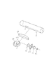
図13は、本実施例におけるfθレンズ6の要部斜視図である。
fθレンズ6は、主走査断面内(主走査方向)においては該fθレンズ6に入射する収束光束を感光ドラム面7上に結像させている。
Next, the fθ lens 6 constituting the imaging optical system LB of the present embodiment will be described.
FIG. 13 is a perspective view of a main part of the fθ lens 6 in the present embodiment.
The fθ lens 6 forms an image of a convergent light beam incident on the fθ lens 6 on the photosensitive drum surface 7 in the main scanning section (main scanning direction).
また、副走査断面内(副走査方向)においては、光偏向器5の偏向面4a上に結像された光束を感光ドラム面7上に再結像させ、面倒れを補正している。
In the sub-scan section (sub-scan direction), the light beam imaged on the deflecting surface 4a of the
fθレンズ6は1枚の結像レンズから成り、主走査断面内において両面が非円弧形状より成っている。 The fθ lens 6 is composed of a single imaging lens, and both surfaces are formed in a non-arc shape in the main scanning section.
そして、図1、図13に示すように主走査断面内において光偏向器5側の面はレンズ光軸(軸上)で光偏向器5側に凸形状であり、被走査面7側の面はレンズ光軸の形状が被走査面7側に凹形状である。
As shown in FIGS. 1 and 13, the surface on the
主走査断面におけるレンズ光軸の形状を上記の如く特定することにより、レンズの主走査断面内における主平面を光偏向器側に寄せることができる為、光偏向器から被走査面までの距離(以下、「光路長」と称す。)を短縮し、小型化することが可能となる。 By specifying the shape of the optical axis of the lens in the main scanning section as described above, the main plane in the main scanning section of the lens can be brought closer to the optical deflector, so the distance from the optical deflector to the surface to be scanned ( Hereinafter, it is referred to as “optical path length”), and the size can be reduced.
さらに、本実施例においてはfθレンズ6に主走査断面内において収束した光束を入射させている為、より一層光路長の短縮を可能としている。 Furthermore, in this embodiment, since the light beam converged in the main scanning section is incident on the fθ lens 6, the optical path length can be further shortened.
具体的な本実施例における光路長は、139.142mmであり、非常に小型な光走査装置を実現している。 A specific optical path length in this embodiment is 139.142 mm, which realizes a very small optical scanning device.
一方、主走査断面内においてfθレンズ6の主走査方向(長手方向)のレンズ周辺部(軸外)の形状は、光偏向器5側の入射面が光偏向器5側に凹形状であり、被走査面7側の出射面が被走査面7側に凸形状である。このような形状に特定することにより、主走査方向のコマ収差を良好に補正するとともに、fθ特性をも良好に補正している。
On the other hand, the shape of the lens peripheral portion (off-axis) in the main scanning direction (longitudinal direction) of the fθ lens 6 in the main scanning section is such that the incident surface on the
このように本実施例においては、主走査断面内においてfθレンズ6の両面の曲率をレンズ光軸(軸上)からレンズ周辺部(軸外)に向かい連続に変化させ、中間部においてその符号を反転させている。 As described above, in this embodiment, the curvatures of both surfaces of the fθ lens 6 are continuously changed from the lens optical axis (on the axis) to the lens peripheral part (off-axis) in the main scanning section, and the sign is changed in the intermediate part. Inverted.
尚、本実施例において上記fθレンズ6の中間部とは、画像中心と画像端との間の任意の像高を走査しているときに光線が通過するレンズ面位置のことである。 In the present embodiment, the intermediate portion of the fθ lens 6 is a lens surface position through which a light beam passes when scanning an arbitrary image height between the image center and the image end.
言い方を換えれば、fθレンズ6の中間部とは、有効部内において、結像光学系の光軸と有効部の端部の間の任意の位置のことである。 In other words, the intermediate portion of the fθ lens 6 is an arbitrary position between the optical axis of the imaging optical system and the end portion of the effective portion in the effective portion.
次にfθレンズ6の副走査断面内の形状について説明する。
今、副走査方向の屈折力を全て被走査面7側の出射面に付加した場合を考えてみる。
Next, the shape of the fθ lens 6 in the sub-scan section will be described.
Consider the case where all the refractive power in the sub-scanning direction is added to the exit surface on the scanned surface 7 side.
副走査断面内においては、前述したように光偏向器5の反射面5a上と被走査面7とが共役関係になっている。
In the sub-scan section, as described above, the reflection surface 5a of the
ここで図1Aと同様な主走査断面を示す図2を参照すると、走査中心部における副走査方向の結像倍率は Here, referring to FIG. 2 showing a main scanning section similar to FIG. 1A, the imaging magnification in the sub-scanning direction at the scanning center is
![]()
![]()
![]()
![]()
図2から解るように、明らかに As you can see from Figure 2, clearly

その結果として、被走査面7上において、副走査方向のスポット径が走査中心部(結像光学系6の光軸)において大きく(走査両端部に比して)、走査両端部において小さくなる(走査中心部に比して)。 As a result, on the surface to be scanned 7, the spot diameter in the sub-scanning direction is large at the scanning center (the optical axis of the imaging optical system 6) (compared to both scanning ends) and small at both scanning ends ( Compared to the scan center).
よって、被走査面7内において副走査方向のスポット径が変化してしまい高画質な画像出力ができなくなってしまうという問題点がある。 Therefore, there is a problem in that the spot diameter in the sub-scanning direction changes within the surface to be scanned 7 and high-quality image output cannot be performed.
また、高速化を達成する為に、光源手段1にマルチビーム半導体レーザ等を使用した場合においては、被走査面7上における複数の結像点の副走査方向のピッチ間隔が走査中心部と走査両端部において異なってしまう。 Further, when a multi-beam semiconductor laser or the like is used as the light source means 1 in order to achieve high speed, the pitch interval in the sub-scanning direction of the plurality of imaging points on the scanned surface 7 is scanned with the scanning center portion. It will be different at both ends.
やはり、高画質な画像出力ができなくなってしまう問題点がある。 After all, there is a problem that high-quality image output cannot be performed.
上記問題点に対しては、fθレンズ6の両面の副走査断面内の曲率をレンズの有効部内において、レンズ光軸(軸上)からレンズ周辺部(軸外)に向かい連続に変化させて、副走査断面内のレンズ形状をベンディングさせることにより副走査断面内の主平面位置を制御して被走査面7に入射する光束の像高による副走査方向の結像倍率の変化を抑える、という手法が有効である。 For the above problem, the curvature in the sub-scan section of both surfaces of the fθ lens 6 is continuously changed from the lens optical axis (on the axis) to the lens peripheral part (off-axis) in the effective part of the lens, A method of controlling the main plane position in the sub-scanning section by bending the lens shape in the sub-scanning section and suppressing the change in the imaging magnification in the sub-scanning direction due to the image height of the light beam incident on the scanned surface 7 Is effective.
本実施例においては、副走査断面内においてfθレンズ6の両面の曲率をレンズ光軸からレンズ周辺部に向かい連続に変化させるだけでなく、両面の副走査断面内の曲率をレンズ光軸(軸上)からレンズ周辺部(軸外)に向かうに従って連続的に変化させ、中間部においてその符号を反転させることによって、より一層の副走査断面の結像倍率を均一にしている。 In the present embodiment, not only the curvature of both surfaces of the fθ lens 6 is continuously changed from the lens optical axis toward the lens periphery in the sub-scan section, but also the curvature in the sub-scan section of both surfaces is changed to the lens optical axis (axis). By continuously changing from the upper part to the lens peripheral part (off-axis) and reversing the sign in the intermediate part, the imaging magnification of a further sub-scan section is made uniform.
ここで、光偏向器5側のレンズ面の中間部と被走査面7側のレンズ面の中間部とは、同一または異なっていても良い。
Here, the intermediate portion of the lens surface on the
本実施例のように、fθレンズ6が比較的光偏向器5に近く、光路長が短い小型な結像光学系の場合には、前記
As in this embodiment, in the case of a small imaging optical system in which the fθ lens 6 is relatively close to the
図3(A),(B)は、各々走査中心部及び走査両端部における副走査断面内のfθレンズ6の形状を示す要部断面図である。
図3(A)は、走査中心部、図3(B)は走査両端部の要部断面図である。
図3(A)の走査中心部においては、光偏向器5側の入射面を光偏向器5側に凹面とした正のパワーのメニスカス形状とし、副走査断面内の主平面を被走査面7側に寄せることにより結像倍率を小さくしている。
FIGS. 3A and 3B are main part cross-sectional views showing the shape of the fθ lens 6 in the sub-scan cross section at the center of scanning and at both ends of the scanning, respectively.
3A is a cross-sectional view of the main part of the scanning center, and FIG.
In the scanning center portion of FIG. 3A, a positive power meniscus shape having an incident surface on the
また、図3(B)の走査両端部においては、被走査面7側の出射面を被走査面7側に凹面とした正のパワーのメニスカス形状とし、副走査断面内の主平面を光偏向器5側に寄せることにより結像倍率を大きくしている。
Further, at both scanning end portions in FIG. 3B, a positive power meniscus shape having an exit surface on the scanned surface 7 side as a concave surface on the scanned surface 7 side, and a main plane in the sub-scan section is optically deflected. The imaging magnification is increased by moving it toward the
これにより、被走査面7上の有効走査領域全域において副走査断面内の結像倍率を一定に保つことを可能としている。 As a result, the imaging magnification in the sub-scanning section can be kept constant over the entire effective scanning area on the scanned surface 7.
即ち、光偏向器5側のレンズ面における光軸上の副走査断面内の曲率半径をr10とするとき、
r10<0 ‥‥(1)
なる条件を満足するようしている。
That is, when the radius of curvature of the sub-scanning section on the optical axis of the lens surface of the
r1 0 <0 (1)
To satisfy the following conditions.
なお、曲率半径(単位はmm)の符号は、曲率中心がその面頂点の右にある場合を正、曲率中心がその面頂点の左にある場合を負と定義する。
曲率は、1/曲率半径にて定義される。
Note that the sign of the radius of curvature (in mm) is defined as positive when the center of curvature is to the right of the surface vertex and negative when the center of curvature is to the left of the surface vertex.
The curvature is defined by 1 / the radius of curvature.
また、図3(B)に示した走査両端部(周辺部)における副走査断面内のレンズ形状は、副走査方向の球面収差が非常に出やすい形状となり、結像スポットのプロファイルが劣化し易くなってしまう。 Further, the lens shape in the sub-scan section at both scanning end portions (peripheral portions) shown in FIG. 3B is a shape in which spherical aberration in the sub-scan direction is very likely to occur, and the profile of the imaging spot is likely to deteriorate. turn into.
そこで、被走査面7側のレンズ面(出射面)の曲率半径をなるべく大きく設定することが好ましい。 Therefore, it is preferable to set the radius of curvature of the lens surface (exit surface) on the scanned surface 7 side as large as possible.
そこで、本実施例においては、走査両端部における副走査方向の球面収差を劣化させないよう、図3(A)に示した光偏向器5側のレンズ面(入射面)の曲率半径よりも、図3(B)に示した被走査面7側のレンズ面(出射面)の曲率半径を大きく設定している。
Therefore, in this embodiment, in order not to deteriorate the spherical aberration in the sub-scanning direction at both scanning ends, the radius of curvature of the lens surface (incident surface) on the
即ち、被走査面7側のレンズ面(出射面)における光軸上の曲率の符号が反転している領域のレンズ有効部内における曲率半径の絶対値の最小値を|r2|minとするとき、
|r10|<|r2|min ‥‥(2)
なる条件を満足するように副走査断面内のレンズ面の形状を特定している。
That is, when the minimum value of the absolute value of the radius of curvature in the lens effective portion in the region where the sign of the curvature on the optical axis on the lens surface (outgoing surface) on the scanned surface 7 side is reversed is | r2 | min ,
| R1 0 | <| r2 | min (2)
The shape of the lens surface in the sub-scan section is specified so as to satisfy the following condition.
これにより、被走査面7上の有効走査領域全域において副走査方向の球面収差を良好に保ちスポットプロファイルの劣化を効果的に防止している。 As a result, the spherical aberration in the sub-scanning direction is satisfactorily maintained throughout the effective scanning area on the scanned surface 7 and the deterioration of the spot profile is effectively prevented.
また、本実施例のようにfθレンズ6の両面の副走査断面内の曲率をレンズ光軸からレンズ周辺部に向かうに従って連続的に変化させ、中間部においてその符号を反転させる形状を採用した場合は、副走査断面内の曲率の変化の割合が比較的大きくなり易い。 Further, when the shape in which the curvature in the sub-scan section of both surfaces of the fθ lens 6 is continuously changed from the lens optical axis toward the lens peripheral portion and the sign is inverted in the intermediate portion as in the present embodiment is adopted. The ratio of the curvature change in the sub-scanning cross section tends to be relatively large.
しかしながら、光束内部において副走査断面内の曲率があまり大きく変化してしまうと図4に示すようにスポットが「おむすび」のような形状に変形し、サイドローブの強度も増加しスポットプロファイルが劣化し易くなる。 However, if the curvature in the sub-scan section changes too much inside the light beam, the spot deforms into a shape like a “muscle” as shown in FIG. 4, the intensity of the side lobe increases, and the spot profile deteriorates. It becomes easy.
そこで本実施例ではそれを防止し良好なるスポットプロファイルを維持する為に、副走査断面内の曲率1/r’をレンズの主走査方向(長手方向)の座標yの関数:1/r’=f(y)で表したとき、該曲率1/r’の一階微分の絶対値が、両面とも
Therefore, in this embodiment, in order to prevent this and maintain a good spot profile, the
これにより光束内部における副走査断面内の曲率の変化量を抑え、スポットプロファイルの劣化を効果的に防止し、高画質な画像出力が可能な光走査装置を実現している。 This realizes an optical scanning device that suppresses the amount of change in the curvature in the sub-scan section within the light beam, effectively prevents the deterioration of the spot profile, and can output a high-quality image.
条件式(3)は、良好なるスポットプロファイルを維持する為の条件である。
条件式(3)の上限値を超えてしまうと光束内部における副走査断面内の曲率の変化量が大きくなり、図4に示した如きスポットの劣化が許容範囲を越えてしまうので好ましくない。
更に好ましくは、上記条件式(3)を次の如く設定するのが良い。
Conditional expression (3) is a condition for maintaining a good spot profile.
Exceeding the upper limit value of conditional expression (3) is not preferable because the amount of change in curvature in the sub-scanning section inside the light beam increases and the spot deterioration as shown in FIG. 4 exceeds the allowable range.
More preferably, the conditional expression (3) is set as follows.
本実施例においては、fθレンズ6に主走査方向に収束した光束を入射させて、より一層光路長の短縮を可能としているが、収束した光束をfθレンズ6に入射させると走査の開始側と終了側でfθ特性に非対称性が発生する。 In this embodiment, the light beam converged in the main scanning direction is made incident on the fθ lens 6 to further reduce the optical path length. However, if the converged light beam is made incident on the fθ lens 6, the scanning start side is set. Asymmetry occurs in the fθ characteristic on the end side.
そこで、本実施例においては、fθレンズ6の光偏向器5側のレンズ面(入射面)の主走査断面内における曲率をレンズ光軸からレンズ周辺部に向かうに従って連続的に非対称に変化させている。
Therefore, in this embodiment, the curvature in the main scanning section of the lens surface (incident surface) of the fθ lens 6 on the
fθレンズ6の光軸上における主走査方向のパワー及び副走査方向のパワーは共に正のパワーである。 The power in the main scanning direction and the power in the sub-scanning direction on the optical axis of the fθ lens 6 are both positive power.
これにより、走査の開始側と終了側のfθ特性の非対称性を良好に補正している。 As a result, the asymmetry of the fθ characteristic between the start side and the end side of scanning is corrected well.
また、光偏向器5の反射面の位置は、光偏向器5の走査に従ってfθレンズ6の光軸方向に移動するが、その移動量は走査の開始側と終了側で対称とはならない為に、副走査方向の像面湾曲が走査の開始側と終了側とで非対称になる。
Further, the position of the reflection surface of the
そこで、本実施例においては、fθレンズ6の光偏向器5側のレンズ面(入射面)の副走査断面内における曲率をレンズ光軸からレンズ周辺部に向かうに従って連続的に非対称に変化させている。
Therefore, in this embodiment, the curvature in the sub-scan section of the lens surface (incident surface) of the fθ lens 6 on the
これにより、走査の開始側と終了側の副走査方向の像面湾曲の非対称性を良好に補正している。 Thereby, the asymmetry of the curvature of field in the sub-scanning direction on the start side and the end side of the scan is corrected well.
また、本実施例におけるfθレンズ6の非球面形状を各レンズ面と光軸との交点を原点とし、光軸方向をX軸、主走査断面内において光軸と直交する軸をY軸、副走査断面内において光軸と直交する軸をZ軸として、fθレンズ6の入射面または出射面の主走査断面内の形状をx=g(y)で表したとき、有効走査領域内の任意の主走査方向のレンズ面位置ymmにおけるxの二階微分値と、主走査方向のレンズ面位置y+0.01mmにおけるxの二階微分値の差の絶対値を、|δd2x/dy2|としたとき、fθレンズ6の入射面及び出射面の両面とも、
|δd2x/dy2|<0.00003 ・・・(4)式
なる条件式を満足するように両面の主走査断面形状を設定している。
Further, in the present embodiment, the aspherical shape of the fθ lens 6 is set such that the intersection of each lens surface and the optical axis is the origin, the optical axis direction is the X axis, and the axis orthogonal to the optical axis in the main scanning section is the Y axis. When an axis orthogonal to the optical axis in the scanning section is the Z-axis and the shape of the incident surface or the exit surface of the fθ lens 6 in the main scanning section is represented by x = g (y), any arbitrary region within the effective scanning area is represented. When the absolute value of the difference between the second-order differential value of x at the lens surface position ymm in the main scanning direction and the second-order differential value of x at the lens surface position y + 0.01 mm in the main scanning direction is | δd2x / dy2 | Both the entrance surface and the exit surface of 6
| Δd2x / dy2 | <0.00003 (2) The main scanning cross-sectional shapes on both sides are set so as to satisfy the conditional expression (4).
入射面及び出射面の両面共に非球面を用いたfθレンズは、プラスチック成形により製作することが好ましい。その場合、各レンズ面の形状を掘り込んだ鏡面駒を成形機にセットして成形することになるが、通常の成形機の場合、各鏡面の相対的な位置の再現性は0.01mm程度の誤差が発生してしまう。 It is preferable that the fθ lens using aspherical surfaces on both the entrance surface and the exit surface is manufactured by plastic molding. In that case, the mirror surface piece that has dug the shape of each lens surface is set in the molding machine, and in the case of a normal molding machine, the reproducibility of the relative position of each mirror surface is about 0.01 mm. Error will occur.
特に、レンズの主走査方向に前記位置誤差が発生すると主走査方向のピントずれが発生してしまう。本実施例においてはfθレンズ6の両面を上記条件式(4)を満足させるような形状とすることによって、上記ピントずれの発生を効率よく防止している。 In particular, when the position error occurs in the main scanning direction of the lens, a focus shift in the main scanning direction occurs. In the present embodiment, the both sides of the fθ lens 6 are shaped so as to satisfy the conditional expression (4), thereby effectively preventing the occurrence of the focus shift.
上記条件式(4)の上限を超えると成形機の各鏡面の相対的な位置の再現性誤差によって性能がバラツキ、安定した性能のfθレンズを生産することが困難となってしまうので良くない。 If the upper limit of the conditional expression (4) is exceeded, the performance varies due to the reproducibility error of the relative position of each mirror surface of the molding machine, and it becomes difficult to produce an fθ lens with stable performance.
表1−1、表1−2に本実施例における光走査装置の光学系の諸特性を示す。 Tables 1-1 and 1-2 show various characteristics of the optical system of the optical scanning device in this example.
本実施例では、被走査面7上の走査線の走査幅が216mm(A4サイズ)程度の場合に光路長150mm以下の光走査装置を実現している。 In this embodiment, an optical scanning device having an optical path length of 150 mm or less is realized when the scanning width of the scanning line on the scanned surface 7 is about 216 mm (A4 size).
fθレンズ6の主走査断面の非球面形状は、各レンズ面と光軸との交点を原点とし、光軸方向をX軸、主走査断面内において光軸と直交する軸をY軸、副走査断面内において光軸と直交する軸をZ軸としたときに、 The aspherical shape of the main scanning section of the fθ lens 6 is based on the intersection of each lens surface and the optical axis as the origin, the optical axis direction is the X axis, and the axis orthogonal to the optical axis in the main scanning section is the Y axis. When the axis perpendicular to the optical axis in the cross section is the Z axis,
尚、Rは曲率半径、k、B4〜B16は非球面係数である。
また、副走査断面の形状は主走査方向のレンズ面座標がYであるところの曲率半径r’が、
R is a radius of curvature, and k and B 4 to B 16 are aspherical coefficients.
Further, the shape of the sub-scanning section is the curvature radius r ′ where the lens surface coordinate in the main scanning direction is Y,
尚、rは光軸上における曲率半径、D2〜D16は各係数である。
また、走査の開始側と終了側で係数が異なる場合は、開始側(図1において上側)の係数には添字uを附し、終了側(図1において下側)の係数には添字lを附している。
Incidentally, r is the radius of curvature,
If the coefficients are different between the start side and the end side of scanning, the subscript u is added to the coefficient on the start side (upper side in FIG. 1), and the subscript l is added to the coefficient on the end side (lower side in FIG. 1). It is attached.
図5は本実施例の主走査方向及び副走査方向の像面湾曲を示す収差図である。
図5において横軸は像高(主走査方向)である。
図5の収差図の縦軸及び横軸共に単位はmmである。
FIG. 5 is an aberration diagram showing field curvature in the main scanning direction and the sub-scanning direction of the present embodiment.
In FIG. 5, the horizontal axis is the image height (main scanning direction).
The unit in both the vertical axis and the horizontal axis of the aberration diagram of FIG. 5 is mm.
図6はfθ特性を示す収差図であり、縦軸には理想像高と実像高の差分をプロットして示している。
図6において横軸は像高(主走査方向)である。
FIG. 6 is an aberration diagram showing the fθ characteristic, and the vertical axis shows the difference between the ideal image height and the real image height plotted.
In FIG. 6, the horizontal axis is the image height (main scanning direction).
本実施例のfθレンズ6においては、光偏向器5側のレンズ面の主走査断面内における曲率をレンズ光軸からレンズ周辺部に向かうに従って連続的に非対称に変化させているので、走査の開始側と終了側のfθ特性の非対称性が良好に補正されている。
In the fθ lens 6 of the present embodiment, the curvature of the lens surface on the
図7は、副走査断面内の結像倍率を示すグラフである。
図7において、横軸は像高(主走査方向)である。
FIG. 7 is a graph showing the imaging magnification in the sub-scan section.
In FIG. 7, the horizontal axis represents the image height (main scanning direction).
本実施例においては、fθレンズ6の両面の副走査断面内の曲率をレンズ光軸からレンズ周辺部に向かうに従って連続的に変化させ、中間部においてその符号を反転させることによってより一層の副走査断面の結像倍率を均一にしている。 In the present embodiment, the curvature in the sub-scan section of both surfaces of the fθ lens 6 is continuously changed from the lens optical axis toward the lens peripheral portion, and the sign is inverted in the intermediate portion, thereby further sub-scanning. The imaging magnification of the cross section is made uniform.
図8は本実施例のfθレンズ6の両面の副走査断面内の曲率半径を、結像レンズ6の主走査方向(長手方向)の座標yを横軸にとってプロットしたグラフである。 FIG. 8 is a graph in which the radii of curvature in the sub-scan section of both surfaces of the fθ lens 6 of this embodiment are plotted with the coordinate y in the main scanning direction (longitudinal direction) of the imaging lens 6 as the horizontal axis.
点線が偏向器5側の入射面の副走査断面内の曲率半径を示し、実線が被走査面7側の出射面の副走査断面内の曲率半径を示す。
The dotted line indicates the radius of curvature in the sub-scan section of the incident surface on the
図8においては、結像レンズ6の両面の副走査断面内の曲率半径の符号がレンズ光軸からレンズ周辺部に向かうに従って連続的に変化して中間部においてその符号が反転していることが解る。 In FIG. 8, the sign of the radius of curvature in the sub-scan section of both surfaces of the imaging lens 6 changes continuously from the lens optical axis toward the lens periphery, and the sign is inverted at the intermediate part. I understand.
ここで、光偏向器5側のレンズ面における光軸上の副走査断面内の曲率半径r10の値はr10=−14.1
であり、これは条件式(1)を満足している。
Here, the value of the curvature radius r1 0 in the sub-scanning section on the optical axis of the lens surface of the
This satisfies the conditional expression (1).
また、被走査面7側のレンズ面(出射面)における光軸上の曲率の符号が反転している領域のレンズ有効部内における曲率半径の絶対値の最小値|r2|minの値は
|r2|min=66.04122
であり、これは条件式(2)をも満足していることが解る。
In addition, the minimum value | r2 | min of the absolute value of the radius of curvature in the lens effective portion in the region where the sign of the curvature on the optical axis on the lens surface (outgoing surface) on the scanned surface 7 side is inverted is | r2 | Min = 66.04122
It can be seen that this also satisfies conditional expression (2).
本実施例のfθレンズ6においては、図3(B)における被走査面7側の副走査断面内の曲率半径をあまり小さくならないような形状とすることにより、走査端部における副走査方向の球面収差のを劣化を防止している。曲率の単位は、1/mmである。 In the fθ lens 6 of this embodiment, a spherical surface in the sub-scanning direction at the scanning end is formed by making the curvature radius in the sub-scanning cross section on the scanning surface 7 side in FIG. The deterioration of the aberration is prevented. The unit of curvature is 1 / mm.
図9は本実施例のfθレンズ6の両面の副走査断面内の曲率1/r’をレンズの主走査方向(長手方向)の座標yの関数:1/r’=f(y)で表したとき、1/r’の一階微分の値
FIG. 9 shows the
このグラフから解るように、光偏向器5側のレンズ面(入射面)および被走査面7側のレンズ面(出射面)ともに、1/r’の一階微分の絶対値
As can be seen from this graph, the absolute value of the first derivative of 1 / r ′ for both the lens surface (incident surface) on the
が条件式(1)を満足しているので、光束内部における副走査断面内の曲率の変化量を抑え、スポットプロファイルの劣化を効果的に防止し、高画質な画像出力が可能な光走査装置を実現している。 Satisfies the conditional expression (1), the amount of change in the curvature in the sub-scanning section inside the light beam is suppressed, the spot profile is effectively prevented from being deteriorated, and an optical scanning device capable of outputting a high-quality image. Is realized.
図14は本実施例のfθレンズ6の両面の座標ymmにおけるxの二階微分値と座標y+0.01mmにおけるxの二階微分値の差の絶対値:|δd2x/dy2|をレンズの主走査方向の座標yを横軸にとってプロットしたグラフである。
図14の横軸は、レンズ面の主走査方向の座標である。
FIG. 14 shows the absolute value of the difference between the second-order differential value of x at the coordinate ymm and the second-order differential value of x at the coordinate y + 0.01 mm of the fθ lens 6 of this embodiment: | δd2x / dy2 | It is the graph which plotted the coordinate y on the horizontal axis.
The horizontal axis in FIG. 14 is the coordinates of the lens surface in the main scanning direction.
このグラフから解るように、入射面及び出射面の両面ともにレンズ面座標ymmにおけるxの二階微分値と座標y+0.01mmにおけるxの二階微分値の差の絶対値が条件式(4)を満足しているため、プラスチック成形により安定した性能のfθレンズを生産することが可能となっている。 As can be seen from this graph, the absolute value of the difference between the second-order differential value of x at the lens surface coordinate ymm and the second-order differential value of x at the coordinate y + 0.01 mm satisfies the conditional expression (4) on both the entrance surface and the exit surface. Therefore, it is possible to produce an fθ lens with stable performance by plastic molding.
図10は本実施例における被走査面7上での各走査位置での結像スポットのプロファイルを示す図である。図の上の数字は走査位置を示し、各スポットの図は結像スポットのピーク強度を1に正規化したとに、0.05、1/e2、1/e、0.5の各強度の断面を示している。一番外側の線が0.05、以下内側に向かうに従って、1/e2、1/e、0.5の強度の断面である。 FIG. 10 is a diagram showing the profile of the imaging spot at each scanning position on the scanning surface 7 in this embodiment. The numbers at the top of the figure indicate the scanning position, and the figure of each spot shows the intensity of 0.05, 1 / e 2 , 1 / e, and 0.5 when the peak intensity of the imaging spot is normalized to 1. The cross section of is shown. The outermost line is 0.05, and the cross section has an intensity of 1 / e 2 , 1 / e, and 0.5 as it goes inward.
図10から解るように、結像スポット形状が良好に補正されており、高画質な画像出力が可能な光走査装置を実現することが可能である。 As can be seen from FIG. 10, it is possible to realize an optical scanning device in which the image spot shape is well corrected and high-quality image output is possible.
特に、小型化が可能でかつ簡易な構成でありながら高画質な画像出力か可能で、さらに複数の発光点を有する光源を使用するマルチビーム走査に好適でかつ高速印字が可能な光走査装置を達成している。 In particular, an optical scanning device capable of high-quality image output while being miniaturized and having a simple configuration, and suitable for multi-beam scanning using a light source having a plurality of light emitting points and capable of high-speed printing. Have achieved.
次に、本発明の光走査装置の実施例2について説明する。
本実施例において前述の実施例1と異なる点は、光源手段を2つの発光点を有するモノリシックなマルチビーム半導体レーザより構成したことである。その他の構成及び光学的作用は実施例1と同様であり、これにより同様な効果を得ている。
Next, a second embodiment of the optical scanning device of the present invention will be described.
The difference between the present embodiment and the first embodiment is that the light source means is composed of a monolithic multi-beam semiconductor laser having two light emitting points. Other configurations and optical functions are the same as those in the first embodiment, and the same effects are obtained.
本実施例においては、2つの発光点を有するモノリシックマルチビーム半導体レーザとしたが、3つ以上の発光点を有するモノリシックマルチビーム半導体レーザも本発明に適用できる。 In this embodiment, the monolithic multi-beam semiconductor laser having two emission points is used, but a monolithic multi-beam semiconductor laser having three or more emission points can also be applied to the present invention.
図7に示したように、実施例1の光走査装置の副走査断面内の結像倍率は有効走査領域内で非常に均一であり、結像光学系の光軸の副走査断面内の結像倍率βs0と周辺部の軸外の副走査断面内の結像倍率βs1とした場合、|(βs1−βs0)/βs0|≦0.1を満たしている。 As shown in FIG. 7, the imaging magnification in the sub-scan section of the optical scanning apparatus of Example 1 is very uniform in the effective scan area, and the connection in the sub-scan section of the optical axis of the imaging optical system. Assuming that the image magnification βs0 and the image formation magnification βs1 in the sub-scanning cross-section off the peripheral axis, | (βs1-βs0) /βs0|≦0.1 is satisfied.
従って、光源手段としてマルチビーム半導体レーザを使用した場合、被走査面7上での副走査方向のビーム間隔が被走査面7上にて有効走査領域全域で均一なものとすることができるので、マルチビーム半導体レーザを使用し、高速化を達成することが可能となる。 Therefore, when a multi-beam semiconductor laser is used as the light source means, the beam interval in the sub-scanning direction on the scanned surface 7 can be uniform over the entire effective scanning region on the scanned surface 7. It is possible to achieve high speed using a multi-beam semiconductor laser.
なお、本実施例で使用しているモノリシックなマルチビーム半導体レーザは、発光点数が2つ、発振波長は790nm、発光点間隔は90μmである。 The monolithic multi-beam semiconductor laser used in this example has two emission points, an oscillation wavelength of 790 nm, and an emission point interval of 90 μm.
被走査面7上において、副走査方向に600DPIの間隔である42.3μmの間隔で各発光点からの結像スポットを配置する為に、図11に示すように半導体レーザを主走査方向に対して角度δ=4.162度だけ傾けて配置している。 On the surface to be scanned 7, in order to arrange the imaging spots from each light emitting point at an interval of 42.3 μm, which is an interval of 600 DPI, in the sub-scanning direction, as shown in FIG. And the angle δ = 4.162 degrees.
このように配置した場合の、被走査面7上での2つのビームの副走査方向の42.3μmに対するピッチ間隔誤差を図12に示す。 FIG. 12 shows a pitch interval error with respect to 42.3 μm in the sub-scanning direction of the two beams on the surface to be scanned 7 when arranged in this way.
図12において縦軸はピッチ間隔誤差量であり、単位はμmである。横軸は像高(主走査方向)である。 In FIG. 12, the vertical axis represents the pitch interval error amount, and the unit is μm. The horizontal axis is the image height (main scanning direction).
図12から解るようにマルチビーム走査を行ったときの副走査方向のピッチ間隔誤差は全域で1μm以下であり、非常に良好に間隔誤差が補正されている為、容易に高速化が達成できる。 As can be seen from FIG. 12, the pitch interval error in the sub-scanning direction when the multi-beam scanning is performed is 1 μm or less over the entire area, and the interval error is corrected very well, so that high speed can be easily achieved.
尚、発光点の数は2つに限らず、例えば3つ以上であっても良い。これにより更に高速化を図ることができる。 The number of light emitting points is not limited to two, and may be three or more, for example. This can further increase the speed.
尚、本実施例1及び2では結像光学系を1枚の結像レンズより構成したが、これに限らず、例えば2枚以上の結像レンズより構成してもよい。 In the first and second embodiments, the imaging optical system is composed of one imaging lens. However, the present invention is not limited to this. For example, the imaging optical system may be composed of two or more imaging lenses.
また、本実施例では主走査断面内の形状が両面とも非円弧形状で形成されている結像レンズを1枚より構成したが、これに限らず、例えば2枚以上で構成してもよい。 Further, in this embodiment, the imaging lens in which the shape in the main scanning section is formed in a non-arc shape on both sides is constituted by one sheet, but the present invention is not limited to this. For example, it may be constituted by two or more sheets.
[画像形成装置]
図15は、本発明の画像形成装置の実施例を示す副走査方向の要部断面図である。図において、符号104は画像形成装置を示す。
[Image forming apparatus]
FIG. 15 is a cross-sectional view of the main part in the sub-scanning direction showing an embodiment of the image forming apparatus of the present invention. In the figure,
この画像形成装置104には、パーソナルコンピュータ等の外部機器117からコードデータDcが入力する。このコードデータDcは、装置内のプリンタコントローラ111によって、画像データ(ドットデータ)Diに変換される。
Code data Dc is input to the
この画像データDiは、実施例1〜3のいずれかに示した構成を有する光走査ユニット100に入力される。
The image data Di is input to the
そして、この光走査ユニット100からは、画像データDiに応じて変調された光ビーム103が出射され、この光ビーム103によって感光ドラム101の感光面が主走査方向に走査される。
The
静電潜像担持体(感光体)たる感光ドラム101は、モータ115によって時計廻りに回転させられる。
The
そして、この回転に伴って、感光ドラム101の感光面が光ビーム103に対して、主走査方向と直交する副走査方向に移動する。
With this rotation, the photosensitive surface of the
感光ドラム101の上方には、感光ドラム101の表面を一様に帯電せしめる帯電ローラ102が表面に当接するように設けられている。
Above the
そして、帯電ローラ102によって帯電された感光ドラム101の表面に、前記光走査ユニット100によって走査される光ビーム103が照射されるようになっている。
The surface of the
先に説明したように、光ビーム103は、画像データDiに基づいて変調されており、この光ビーム103を照射することによって感光ドラム101の表面に静電潜像を形成せしめる。
As described above, the
この静電潜像は、上記光ビーム103の照射位置よりもさらに感光ドラム101の回転方向の下流側で感光ドラム101に当接するように配設された現像器107によってトナー像として現像される。
The electrostatic latent image is developed as a toner image by a developing
現像器107によって現像されたトナー像は、感光ドラム101の下方で、感光ドラム101に対向するように配設された転写ローラ108によって被転写材たる用紙112上に転写される。
The toner image developed by the developing
用紙112は感光ドラム101の前方(図15において右側)の用紙カセット109内に収納されているが、手差しでも給紙が可能である。用紙カセット109端部には、給紙ローラ110が配設されており、用紙カセット109内の用紙112を搬送路へ送り込む。
The
以上のようにして、未定着トナー像を転写された用紙112はさらに感光ドラム101後方(図15において左側)の定着器へと搬送される。
As described above, the
定着器は内部に定着ヒータ(図示せず)を有する定着ローラ113とこの定着ローラ113に圧接するように配設された加圧ローラ114とで構成されており、転写部から搬送されてきた用紙112を定着ローラ113と加圧ローラ114の圧接部にて加圧しながら加熱することにより用紙112上の未定着トナー像を定着せしめる。
The fixing device includes a fixing
更に定着ローラ113の後方には排紙ローラ116が配設されており、定着された用紙112を画像形成装置の外に排出せしめる。
Further, a
図15においては図示していないが、プリントコントローラ111は、先に説明したデータの変換だけでなく、モータ115を始め画像形成装置内の各部や、後述する光走査ユニット内のポリゴンモータなどの制御を行う。
Although not shown in FIG. 15, the
本発明で使用される画像形成装置の記録密度は、特に限定されない。 The recording density of the image forming apparatus used in the present invention is not particularly limited.
しかし、記録密度が高くなればなるほど、高画質が求められることを考えると、1200dpi以上の画像形成装置において本発明の実施例1〜2の構成はより効果を発揮する。 However, considering that the higher the recording density is, the higher the image quality is required, the configurations of the first and second embodiments of the present invention are more effective in an image forming apparatus of 1200 dpi or more.
[カラー画像形成装置]
図16は、本発明の実施例のカラー画像形成装置の要部概略図である。本実施例は、光走査装置を4個並べ各々並行して像担持体である感光ドラム面上に画像情報を記録するタンデムタイプのカラー画像形成装置である。
[Color image forming apparatus]
FIG. 16 is a schematic diagram of a main part of a color image forming apparatus according to an embodiment of the present invention. This embodiment is a tandem type color image forming apparatus in which four optical scanning devices are arranged in parallel and image information is recorded on a photosensitive drum surface as an image carrier.
図16において、60はカラー画像形成装置、11、12、13、14は各々実施例1〜3に示したいずれかの構成を有する光走査装置、21、22、23、24は各々像担持体としての感光ドラム、31、32、33、34は各々現像器、51は搬送ベルトである。
In FIG. 16, 60 is a color image forming apparatus, 11, 12, 13, and 14 are optical scanning devices each having one of the configurations shown in
図16において、カラー画像形成装置60には、パーソナルコンピュータ等の外部機器52からR(レッド)、G(グリーン)、B(ブルー)の各色信号が入力する。 In FIG. 16, R (red), G (green), and B (blue) color signals are input to the color image forming apparatus 60 from an external device 52 such as a personal computer.
これらの色信号は、装置内のプリンタコントローラ53によって、C(シアン)、M(マゼンタ)、Y(イエロー)、K(ブラック)の各画像データ(ドットデータ)に変換される。 These color signals are converted into C (cyan), M (magenta), Y (yellow), and K (black) image data (dot data) by a printer controller 53 in the apparatus.
これらの画像データは、それぞれ光走査装置11、12、13、14に入力される。
These image data are input to the
そして、これらの光走査装置からは、各画像データに応じて変調された光ビーム41、42、43、44が出射され、これらの光ビームによって感光ドラム21、22、23、24の感光面が主走査方向に走査される。
From these optical scanning devices, light beams 41, 42, 43, and 44 modulated according to each image data are emitted, and the photosensitive surfaces of the
本実施例におけるカラー画像形成装置は光走査装置(11、12、13、14)を4個並べ、各々がC(シアン)、M(マゼンタ)、Y(イエロー)、K(ブラック)の各色に対応し、各々平行して感光ドラム21、22、23、24面上に画像信号(画像情報)を記録し、カラー画像を高速に印字するものである。
The color image forming apparatus in this embodiment has four optical scanning devices (11, 12, 13, and 14) arranged in each color of C (cyan), M (magenta), Y (yellow), and K (black). Correspondingly, image signals (image information) are recorded on the
本実施例におけるカラー画像形成装置は上述の如く4つの光走査装置11、12、13、14により各々の画像データに基づいた光ビームを用いて各色の潜像を各々対応する感光ドラム21、22、23、24面上に形成している。
As described above, the color image forming apparatus in this embodiment uses the light beams based on the respective image data by the four
その後、記録材に多重転写して1枚のフルカラー画像を形成している。 Thereafter, a single full color image is formed by multiple transfer onto a recording material.
前記外部機器52としては、例えばCCDセンサを備えたカラー画像読取装置が用いられても良い。この場合には、このカラー画像読取装置と、カラー画像形成装置60とで、カラーデジタル複写機が構成される。 As the external device 52, for example, a color image reading device including a CCD sensor may be used. In this case, the color image reading apparatus and the color image forming apparatus 60 constitute a color digital copying machine.
1 光源手段(半導体レーザー)
2 開口絞り
3 集光光学系(集光レンズ)
4 レンズ系(シリンドリカルレンズ)
5 偏向手段(回転多面鏡)
LA 入射光学系
LB 結像光学系
6 結像レンズ
7 被走査面(感光ドラム面)
11、12、13、14 光走査装置
21、22、23、24 像担持体(感光ドラム)
31、32、33、34 現像器
41、42、43、44 光束
51 搬送ベルト
52 外部機器
53 プリンタコントローラ
60 カラー画像形成装置
100 光走査装置
101 感光ドラム
102 帯電ローラ
103 光ビーム
104 画像形成装置
107 現像装置
108 転写ローラ
109 用紙カセット
110 給紙ローラ
111 プリンタコントローラ
112 転写材(用紙)
113 定着ローラ
114 加圧ローラ
115 モータ
116 排紙ローラ
117 外部機器
1 Light source means (semiconductor laser)
2
4 Lens system (cylindrical lens)
5 Deflection means (rotating polygon mirror)
LA incident optical system LB imaging optical system 6 imaging lens 7 surface to be scanned (photosensitive drum surface)
11, 12, 13, 14
31, 32, 33, 34
113 Fixing Roller 114
Claims (23)
副走査断面内において、該結像光学系は、該偏向手段の偏向面と該被走査面とを共役な関係としており、
該結像光学系を構成する少なくとも1つの結像光学素子の入射面及び出射面の両面の副走査断面内の曲率が有効部内において、該結像光学系の光軸から周辺部に向かうに従って連続的に変化しており、且つ、該結像光学素子の入射面及び出射面の両面の副走査断面内の曲率は、該有効部内において、曲率のその符号が反転しており、
該結像光学素子の入射面における光軸上の副走査断面内の曲率半径をr10、有効部内において、該結像光学素子の出射面における光軸上の副走査断面内の曲率に対して符号が反転している領域の副走査断面内の曲率半径の絶対値の最小値を|r2|minとするとき、
r10<0
|r10|<|r2|min
且つ、該結像光学素子の入射面又は出射面の主走査断面内の形状xを該結像光学素子の有効走査領域内の任意の主走査方向の座標yの関数:x=g(y)で表したとき、座標yにおけるxの二階微分値と座標y+0.01におけるxの二階微分値の差の絶対値を、|δd2x/dy2|としたとき、該入射面及び出射面の両面とも、
|δd2x/dy2|<0.00003
なる条件を満足することを特徴とする光走査装置。 An optical scanning device comprising: a light source means; a deflecting means for deflecting a light beam emitted from the light source means in the main scanning direction; and an imaging optical system for forming an image on the surface to be scanned. In
In the sub-scan section, the imaging optical system has a conjugate relationship between the deflection surface of the deflection means and the surface to be scanned.
The curvature in the sub-scan section of both the entrance surface and the exit surface of at least one image forming optical element constituting the image forming optical system is continuous in the effective portion from the optical axis of the image forming optical system toward the peripheral portion. And the curvature in the sub-scan section of both the entrance surface and the exit surface of the imaging optical element is inverted in the sign of the curvature in the effective portion,
The radius of curvature in the sub-scan section on the optical axis at the entrance surface of the imaging optical element is r1 0 , and the curvature in the sub-scan section on the optical axis at the exit surface of the imaging optical element in the effective portion. When | r2 | min is the minimum absolute value of the radius of curvature in the sub-scan section of the region where the sign is inverted,
r1 0 <0
| R1 0 | <| r2 | min
In addition, the shape x in the main scanning section of the entrance surface or the exit surface of the imaging optical element is a function of an arbitrary coordinate y in the main scanning direction within the effective scanning area of the imaging optical element: x = g (y) When the absolute value of the difference between the second-order differential value of x at the coordinate y and the second-order differential value of x at the coordinate y + 0.01 is | δd2x / dy2 |, both the incident surface and the exit surface are
| Δd2x / dy2 | <0.00003
An optical scanning device characterized by satisfying the following conditions.
副走査断面内において、該結像光学系は、該偏向手段の偏向面と該被走査面とを共役な関係としており、
該結像光学素子を構成する少なくとも1つの結像光学素子の入射面の光軸の主走査断面内の形状が該偏向手段側に凸形状、副走査断面内の形状が該偏向手段側に凹形状であり、
該結像光学素子の入射面の周辺部の主走査断面内の形状が該偏向手段側に凹形状、副走査断面内の形状が該偏向手段側に凸形状であり、
該結像光学素子の出射面の光軸の主走査断面内の形状が該被走査面側に凹形状、副走査断面内の形状が該被走査面側に凸形状であり、
該結像光学素子の出射面の周辺部の主走査断面内の形状が被走査面側に凸形状、副走査断面内の形状が該被走査面側に凹形状であり、
該結像光学素子の入射面又は出射面の主走査断面内の形状xを該結像光学素子の有効走査領域内の任意の主走査方向の座標yの関数:x=g(y)で表したとき、座標yにおけるxの二階微分値と座標y+0.01におけるxの二階微分値の差の絶対値を、|δd2x/dy2|としたとき、該入射面及び出射面の両面とも、
|δd2x/dy2|<0.00003
なる条件を満足することを特徴とする光走査装置。 An optical scanning device comprising: a light source means; a deflecting means for deflecting a light beam emitted from the light source means in the main scanning direction; and an imaging optical system for forming an image on the surface to be scanned. In
In the sub-scan section, the imaging optical system has a conjugate relationship between the deflection surface of the deflection means and the surface to be scanned.
The shape in the main scanning section of the optical axis of the incident surface of at least one imaging optical element constituting the imaging optical element is convex on the deflecting means side, and the shape in the sub-scanning section is concave on the deflecting means side. Shape,
The shape in the main scanning section of the periphery of the incident surface of the imaging optical element is concave on the deflecting means side, and the shape in the sub-scanning section is convex on the deflecting means side,
The shape in the main scanning section of the optical axis of the exit surface of the imaging optical element is concave on the scanned surface side, and the shape in the sub-scanning section is convex on the scanned surface side,
The shape in the main scanning section of the periphery of the exit surface of the imaging optical element is convex on the scanned surface side, and the shape in the sub-scanning section is concave on the scanned surface side,
The shape x in the main scanning section of the incident surface or the exit surface of the imaging optical element is expressed by a function of an arbitrary coordinate y in the main scanning direction in the effective scanning region of the imaging optical element: x = g (y) When the absolute value of the difference between the second-order differential value of x at the coordinate y and the second-order differential value of x at the coordinate y + 0.01 is | δd2x / dy2 |, both the incident surface and the exit surface are
| Δd2x / dy2 | <0.00003
An optical scanning device characterized by satisfying the following conditions.
r10<0
|r10|<|r2|min
なる条件を満足することを特徴とする請求項14に記載の光走査装置。 The radius of curvature of the sub-scan section on the optical axis at the exit surface of the imaging optical element is r1 0 , and the sign is inverted with respect to the curvature on the optical axis at the exit surface of the imaging optical element in the effective portion. When the minimum absolute value of the radius of curvature of the region is | r2 | min ,
r1 0 <0
| R1 0 | <| r2 | min
The optical scanning device according to claim 14, wherein the following condition is satisfied.
23. The color image forming apparatus according to claim 22, further comprising a printer controller that converts color signals input from an external device into image data of different colors and inputs the data to each optical scanning device.
Priority Applications (2)
| Application Number | Priority Date | Filing Date | Title |
|---|---|---|---|
| JP2006067782A JP2006330688A (en) | 2005-04-25 | 2006-03-13 | Optical scanner and image forming apparatus using the same |
| US11/410,095 US7149019B2 (en) | 2005-04-25 | 2006-04-25 | Optical scanning system and image forming apparatus using the same |
Applications Claiming Priority (2)
| Application Number | Priority Date | Filing Date | Title |
|---|---|---|---|
| JP2005126491 | 2005-04-25 | ||
| JP2006067782A JP2006330688A (en) | 2005-04-25 | 2006-03-13 | Optical scanner and image forming apparatus using the same |
Publications (2)
| Publication Number | Publication Date |
|---|---|
| JP2006330688A true JP2006330688A (en) | 2006-12-07 |
| JP2006330688A5 JP2006330688A5 (en) | 2009-04-16 |
Family
ID=37186558
Family Applications (1)
| Application Number | Title | Priority Date | Filing Date |
|---|---|---|---|
| JP2006067782A Withdrawn JP2006330688A (en) | 2005-04-25 | 2006-03-13 | Optical scanner and image forming apparatus using the same |
Country Status (2)
| Country | Link |
|---|---|
| US (1) | US7149019B2 (en) |
| JP (1) | JP2006330688A (en) |
Cited By (1)
| Publication number | Priority date | Publication date | Assignee | Title |
|---|---|---|---|---|
| JP2020030236A (en) * | 2018-08-20 | 2020-02-27 | キヤノン株式会社 | Optical scanner and image forming apparatus |
Families Citing this family (5)
| Publication number | Priority date | Publication date | Assignee | Title |
|---|---|---|---|---|
| US7428088B2 (en) * | 2004-10-28 | 2008-09-23 | Canon Kabushiki Kaisha | Optical scanning apparatus and method for adjusting the same |
| JP2008170487A (en) * | 2007-01-06 | 2008-07-24 | Canon Inc | Optical scanner and image forming apparatus using the same |
| JP4883795B2 (en) * | 2007-06-28 | 2012-02-22 | キヤノン株式会社 | Multi-beam optical scanning device and image forming apparatus using the same |
| JP5046760B2 (en) * | 2007-07-04 | 2012-10-10 | キヤノン株式会社 | Optical scanning device and image forming apparatus using the same |
| JP5079060B2 (en) * | 2010-08-02 | 2012-11-21 | シャープ株式会社 | Optical scanning apparatus and image forming apparatus |
Family Cites Families (6)
| Publication number | Priority date | Publication date | Assignee | Title |
|---|---|---|---|---|
| JP3188053B2 (en) * | 1993-06-28 | 2001-07-16 | 株式会社東芝 | Optical scanning device |
| JP3003065B2 (en) | 1994-05-10 | 2000-01-24 | セイコーエプソン株式会社 | Optical scanning device |
| JP3445050B2 (en) | 1995-02-28 | 2003-09-08 | キヤノン株式会社 | Scanning optical device and multi-beam scanning optical device |
| JP3546898B2 (en) | 1995-01-30 | 2004-07-28 | セイコーエプソン株式会社 | Optical scanning device |
| JP3712017B2 (en) | 1995-05-12 | 2005-11-02 | セイコーエプソン株式会社 | Optical scanning device |
| JP3559684B2 (en) * | 1997-06-13 | 2004-09-02 | キヤノン株式会社 | Optical element and scanning optical device using the same |
-
2006
- 2006-03-13 JP JP2006067782A patent/JP2006330688A/en not_active Withdrawn
- 2006-04-25 US US11/410,095 patent/US7149019B2/en not_active Expired - Fee Related
Cited By (2)
| Publication number | Priority date | Publication date | Assignee | Title |
|---|---|---|---|---|
| JP2020030236A (en) * | 2018-08-20 | 2020-02-27 | キヤノン株式会社 | Optical scanner and image forming apparatus |
| JP7134783B2 (en) | 2018-08-20 | 2022-09-12 | キヤノン株式会社 | Optical scanning device and image forming device |
Also Published As
| Publication number | Publication date |
|---|---|
| US7149019B2 (en) | 2006-12-12 |
| US20060238849A1 (en) | 2006-10-26 |
Similar Documents
| Publication | Publication Date | Title |
|---|---|---|
| JP4819392B2 (en) | Scanning optical device and image forming apparatus using the same | |
| JP4769734B2 (en) | Optical scanning device and image forming apparatus using the same | |
| JP4970864B2 (en) | Optical scanning device, optical writing device including the optical scanning device, and image forming device including the optical scanning device or the optical writing device | |
| JP5171029B2 (en) | Optical scanning device and image forming apparatus using the same | |
| JP2007114484A (en) | Optical scanner and image forming device using it | |
| JP4819436B2 (en) | Optical scanning device and method of adjusting optical scanning device | |
| JP2009271353A (en) | Optical scanner and image forming apparatus using the same | |
| JP2003021802A (en) | Scanning optical device and image forming device using the same | |
| US7142339B2 (en) | Multi-beam optical scanning apparatus and image forming apparatus using the same | |
| JP2006330581A (en) | Multibeam optical scanner and image forming apparatus using the same | |
| JP5896651B2 (en) | Optical scanning device and image forming apparatus using the same | |
| JP4898203B2 (en) | Optical scanning device and image forming apparatus using the same | |
| JP2006330688A (en) | Optical scanner and image forming apparatus using the same | |
| JP4378081B2 (en) | Optical scanning device and image forming apparatus using the same | |
| JP5127122B2 (en) | Method for adjusting scanning line pitch interval of scanning optical device | |
| JP2004070109A (en) | Optical scanner and image forming apparatus using the same | |
| JP4434547B2 (en) | Scanning optical device and image forming apparatus using the same | |
| JP2008052197A (en) | Optical scanner and image forming apparatus using the same | |
| JP5094221B2 (en) | Optical scanning device and image forming apparatus using the same | |
| JP2005070125A (en) | Optical scanner and image forming apparatus using same | |
| JP4378416B2 (en) | Scanning optical device and image forming apparatus using the same | |
| JP2004317790A (en) | Optical scanner | |
| JP4401950B2 (en) | Optical scanning device and image forming apparatus using the same | |
| JP2007102237A (en) | Optical scanner and image forming apparatus using same | |
| JP5441938B2 (en) | Scanning optical device and image forming apparatus using the same |
Legal Events
| Date | Code | Title | Description |
|---|---|---|---|
| A521 | Request for written amendment filed |
Free format text: JAPANESE INTERMEDIATE CODE: A523 Effective date: 20090302 |
|
| A621 | Written request for application examination |
Free format text: JAPANESE INTERMEDIATE CODE: A621 Effective date: 20090302 |
|
| RD04 | Notification of resignation of power of attorney |
Free format text: JAPANESE INTERMEDIATE CODE: A7424 Effective date: 20100201 |
|
| RD01 | Notification of change of attorney |
Free format text: JAPANESE INTERMEDIATE CODE: A7421 Effective date: 20100630 |
|
| A761 | Written withdrawal of application |
Free format text: JAPANESE INTERMEDIATE CODE: A761 Effective date: 20100819 |