JP2006276485A - Aperture member, optical scanning system with same, and image-reading device and image-forming apparatus with the optical scanning system - Google Patents
Aperture member, optical scanning system with same, and image-reading device and image-forming apparatus with the optical scanning system Download PDFInfo
- Publication number
- JP2006276485A JP2006276485A JP2005095925A JP2005095925A JP2006276485A JP 2006276485 A JP2006276485 A JP 2006276485A JP 2005095925 A JP2005095925 A JP 2005095925A JP 2005095925 A JP2005095925 A JP 2005095925A JP 2006276485 A JP2006276485 A JP 2006276485A
- Authority
- JP
- Japan
- Prior art keywords
- laser
- sheet
- optical system
- antireflection structure
- laser beam
- Prior art date
- Legal status (The legal status is an assumption and is not a legal conclusion. Google has not performed a legal analysis and makes no representation as to the accuracy of the status listed.)
- Pending
Links
Images


Landscapes
- Laser Beam Printer (AREA)
- Mechanical Optical Scanning Systems (AREA)
- Surface Treatment Of Optical Elements (AREA)
Abstract
Description
本発明は、レーザ光を走査する走査光学系及びそれに用いられる光学部材に関し、より特定的には、レーザプリンタ、レーザファクシミリ、デジタル複写機等の画像形成装置の露光光学系やスキャナ等の読取光学系に用いられる走査光学系及びそれに用いられるアパーチャ部材に関する。また、本発明は、走査光学系を備える画像形成装置及び画像読取装置に関する。 The present invention relates to a scanning optical system for scanning a laser beam and an optical member used therefor, and more specifically, an exposure optical system of an image forming apparatus such as a laser printer, a laser facsimile, a digital copying machine, or a reading optical such as a scanner. The present invention relates to a scanning optical system used in the system and an aperture member used therefor. The present invention also relates to an image forming apparatus and an image reading apparatus provided with a scanning optical system.
一般的に、レーザプリンタなどに用いられている多くの走査光学系は、光源としての半導体レーザと、レーザ光を走査する光偏向器としての回転多面鏡(ポリゴンミラー)と、半導体レーザ及び回転多面鏡の間に配置され、回転多面鏡の偏向面上に線像を形成する第1結像光学系と、回転多面鏡で偏向走査されたレーザ光を被走査面上へ結像させる走査光学系とを備える。このような構成を有する従来の走査光学系は、さらに、半導体レーザ及び回転多面鏡の間に配置され、レーザ光を所望のビーム径で被走査面上に集光するための光学部材(アパーチャ部材)を備える。 In general, many scanning optical systems used in laser printers, etc. include a semiconductor laser as a light source, a rotating polygon mirror (polygon mirror) as an optical deflector that scans laser light, a semiconductor laser, and a rotating polygon. A first imaging optical system that is arranged between the mirrors and forms a line image on the deflection surface of the rotary polygon mirror; and a scanning optical system that forms an image of the laser beam deflected and scanned by the rotary polygon mirror on the surface to be scanned With. The conventional scanning optical system having such a configuration is further arranged between the semiconductor laser and the rotary polygon mirror, and is an optical member (aperture member) for condensing the laser beam on the scanning surface with a desired beam diameter. ).
例えば、特許文献1及び特許文献2には、アパーチャ部材を備える走査光学系が記載されている。これらの走査光学系において、レーザ光が到達するアパーチャ部材の表面は、通常、例えば黒色材料等のレーザ光を吸収可能な材料からなる。これにより、不要なレーザ光の反射を抑制することができる。
しかしながら、アパーチャ部材の表面を覆うレーザ光を吸収可能な材料は、アパーチャ部材の表面に到達するレーザ光をある程度吸収することはできるものの、当該レーザ光を実質的に完全に吸収することができない。したがって、従来の走査光学系では、半導体レーザから出射されたレーザ光がアパーチャ部材の遮光部と空気との界面で反射することによって不要光が生じる。この不要光が半導体レーザに戻った場合、半導体レーザの光共振器を構成するミラーとアパーチャ部材とが外部共振器を形成することにより、半導体レーザの出力が一定周期で変動してしまう。このように出力が変動する走査光学系を、例えばレーザプリンタなどの画像形成装置に適用した場合、出力される画像に濃度むらが発生し、画質が劣化してしまう。また、出力が変動する走査光学系を、例えばスキャナなどの画像読取装置に適用した場合には、読み取り不良が発生してしまう。 However, the material that can absorb the laser beam covering the surface of the aperture member can absorb the laser beam reaching the surface of the aperture member to some extent, but cannot absorb the laser beam substantially completely. Therefore, in the conventional scanning optical system, unnecessary light is generated by reflecting the laser beam emitted from the semiconductor laser at the interface between the light shielding portion of the aperture member and the air. When this unnecessary light returns to the semiconductor laser, the mirror and the aperture member constituting the optical resonator of the semiconductor laser form an external resonator, so that the output of the semiconductor laser fluctuates at a constant period. When the scanning optical system whose output varies as described above is applied to an image forming apparatus such as a laser printer, for example, density unevenness occurs in the output image, and the image quality deteriorates. Further, when a scanning optical system whose output varies is applied to an image reading apparatus such as a scanner, a reading defect occurs.
それゆえに、本発明の目的は、不要なレーザ光の反射を抑制し、かつ不要なレーザ光を実質的に完全に吸収することができるアパーチャ部材、それを備える走査光学系、並びに走査光学系を備える画像読取装置及び画像形成装置を提供することである。 Therefore, an object of the present invention is to provide an aperture member that can suppress reflection of unnecessary laser light and substantially completely absorb unnecessary laser light, a scanning optical system including the aperture member, and a scanning optical system. An image reading apparatus and an image forming apparatus are provided.
本発明は、レーザ光の光路上に設けられる光学部材であって、レーザ光の光軸に対して垂直な面と、レーザ光の光束を通過させるための開口部とを備え、レーザ光が入射する垂直な面の少なくとも一部に、所定の形状を有する構造単位がレーザ光の波長よりも小さいピッチで周期的にアレイ状に配列された反射防止構造体が設けられ、反射防止構造体自体、及び光学部材の反射防止構造体が設けられた部分のうち、少なくとも一方は、レーザ光を吸収可能な材料からなることを特徴とする。 The present invention is an optical member provided on the optical path of a laser beam, and includes a surface perpendicular to the optical axis of the laser beam and an opening for allowing the laser beam to pass therethrough. An antireflection structure in which structural units having a predetermined shape are periodically arranged in an array at a pitch smaller than the wavelength of the laser light is provided on at least a part of the vertical surface, and the antireflection structure itself, And at least one of the portions of the optical member provided with the antireflection structure is made of a material capable of absorbing laser light.
また、反射防止構造体はシート上に形成されており、光学部材が備える垂直な面のうち、レーザ光が入射する面の少なくとも一部にシートが貼付されていてもよい。 Further, the antireflection structure is formed on the sheet, and the sheet may be attached to at least a part of the surface on which the laser beam is incident among the vertical surfaces of the optical member.
一例として、シートは、レーザ光を吸収可能な材料からなる。他の例として、シートは、透明材料からなり、かつシートが貼付される光学部材は、レーザ光を吸収可能な材料からなる。 As an example, the sheet is made of a material that can absorb laser light. As another example, the sheet is made of a transparent material, and the optical member to which the sheet is attached is made of a material that can absorb laser light.
好ましくは、反射防止構造体の構造単位が、少なくともピッチ以上の高さを有し、より好ましくは、少なくともピッチの3倍以上の高さを有するとよい。 Preferably, the structural unit of the antireflection structure has a height of at least the pitch, and more preferably has a height of at least three times the pitch.
好ましくは、反射防止構造体の構造単位が、略錐状の突出形状及び/または略錐状の陥没構造であるとよい。また、反射防止構造体の底面形状が、略円形、略矩形及び略正六角形からなる群から選ばれる1つであってもよい。 Preferably, the structural unit of the antireflection structure is a substantially conical protruding shape and / or a substantially conical depressed structure. Further, the bottom shape of the antireflection structure may be one selected from the group consisting of a substantially circular shape, a substantially rectangular shape, and a substantially regular hexagonal shape.
一例として、レーザ光を吸収可能な材料が、レーザ光を吸収するための染料を含有する。 As an example, the material capable of absorbing laser light contains a dye for absorbing laser light.
好ましくは、シートと、当該シートが貼付される基材との屈折率の差が0.2以下、より好ましくは、0.1以下であるとよい。 Preferably, the difference in refractive index between the sheet and the substrate to which the sheet is attached is 0.2 or less, more preferably 0.1 or less.
本発明は、上記の光学部材が内部に設けられたことを特徴とする、レーザ光学系である。一例として、レーザ光学系は、走査光学系である。 The present invention is a laser optical system in which the above-described optical member is provided inside. As an example, the laser optical system is a scanning optical system.
上記のレーザ光学系において、反射防止構造体はシート上に形成されており、光学部材が備える垂直な面のうち、レーザ光が入射する面の少なくとも一部にシートが貼付されていてもよい。 In the laser optical system described above, the antireflection structure is formed on the sheet, and the sheet may be attached to at least a part of the surface on which the laser beam is incident among the vertical surfaces of the optical member.
上記のレーザ光学系において、一例として、シートは、レーザ光を吸収可能な材料からなる。また、他の例として、シートは、透明材料からなり、かつシートが貼付される光学部材は、レーザ光を吸収可能な材料からなる。 In the above laser optical system, as an example, the sheet is made of a material capable of absorbing laser light. As another example, the sheet is made of a transparent material, and the optical member to which the sheet is attached is made of a material that can absorb laser light.
上記のレーザ光学系において、好ましくは、反射防止構造体の構造単位が、少なくともピッチ以上の高さを有し、より好ましくは、少なくともピッチの3倍以上の高さを有するとよい。 In the laser optical system described above, the structural unit of the antireflection structure preferably has a height of at least a pitch, and more preferably has a height of at least three times the pitch.
上記のレーザ光学系において、好ましくは、反射防止構造体の構造単位が、略錐状の突出形状及び/または略錐状の陥没構造であるとよい。また、反射防止構造体の底面形状が、略円形、略矩形及び略正六角形からなる群から選ばれる1つであってもよい。 In the above laser optical system, the structural unit of the antireflection structure is preferably a substantially conical protruding shape and / or a substantially conical depressed structure. Further, the bottom shape of the antireflection structure may be one selected from the group consisting of a substantially circular shape, a substantially rectangular shape, and a substantially regular hexagonal shape.
上記のレーザ光学系において、一例として、レーザ光を吸収可能な材料が、レーザ光を吸収するための染料を含有する。 In the above laser optical system, as an example, a material capable of absorbing laser light contains a dye for absorbing laser light.
上記のレーザ光学系において、好ましくは、シートと、当該シートが貼付される基材との屈折率の差が0.2以下、より好ましくは、0.1以下であるとよい。 In the above laser optical system, the difference in refractive index between the sheet and the substrate to which the sheet is attached is preferably 0.2 or less, more preferably 0.1 or less.
また、本発明は、上記のレーザ光学系を用いた画像読取装置である。また、本発明は、上記のレーザ光学系を用いた画像形成装置である。 The present invention is also an image reading apparatus using the laser optical system described above. Further, the present invention is an image forming apparatus using the laser optical system described above.
本発明によれば、不要なレーザ光の反射を抑制し、かつ不要なレーザ光を実質的に完全に吸収することができるアパーチャ部材、それを備える走査光学系、並びに走査光学系を備える画像読取装置及び画像形成装置が提供される。 According to the present invention, an aperture member capable of suppressing reflection of unnecessary laser light and substantially completely absorbing unnecessary laser light, a scanning optical system including the aperture member, and an image reading including the scanning optical system are provided. An apparatus and an image forming apparatus are provided.
以下、図面を参照し、本発明についてさらに具体的に説明する。
(第1の実施形態)
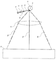
図1は、本発明の第1の実施形態に係るアパーチャ部材10、及び当該アパーチャ部材10が適用される走査光学系の構成を示す図である。本実施形態では、アパーチャ部材10が走査光学系に適用される場合を例に説明する。図1において、走査光学系は、コリメータレンズ72と、アパーチャ部材10と、シリンドリカルレンズ73と、回転多面鏡75と、走査レンズ77とを備える。
Hereinafter, the present invention will be described more specifically with reference to the drawings.
(First embodiment)
FIG. 1 is a diagram showing the configuration of an
走査光学系は、コリメータレンズ72とシリンドリカルレンズ73とにより第1結像光学系を構成し、走査レンズ77により第2結像光学系を構成する。第1結像光学系及び第2結像光学系は、いずれも主走査方向及び主走査方向に直交する副走査方向にそれぞれ異なる光学的パワーを持つアナモフィック光学系である。なお、図1は、回転多面鏡75による主走査を行う主走査面及び走査光学系の光軸を含む平面と紙面とが平行になるように記載されている。
In the scanning optical system, the
コリメータレンズ72は、光源である半導体レーザ71から出射されたレーザ光を略平行収束性のレーザ光に変換する。コリメータレンズ72は、光源側及びポリゴンミラー側とも光軸について回転軸対象形状のレンズである。また、コリメータレンズ72は、樹脂製であり、回転多面鏡側の面に回折による光学的なパワーを備えた回折面が形成されている。なお、半導体レーザ71とコリメータレンズ72との間には、平行板であるカバーガラス(図示せず)が配置される。
The
シリンドリカルレンズ73は、樹脂製であり、半導体レーザ71及び回転多面鏡75との間に配置され、副走査方向に屈折力を持つ。シリンドリカルレンズ73は、副走査方向にのみ光学的パワーを備えた光源側のシリンドリカル面と、ポリゴンミラー側に形成された平面とを持つ。シリンドリカルレンズ73は、コリメータレンズ72から出射された収束性のレーザ光の副走査方向にのみ作用し、回転多面鏡75の反射面の近傍で主走査方向に延びた線状に集光する。
The
アパーチャ部材10は、コリメータレンズ72とシリンドリカルレンズ73との間に配置され、レーザ光の光軸に対して垂直な面と、コリメータレンズ72から出射されたレーザ光の光束を制限するためのアパーチャ(開口部)とを有する。開口部の大きさを調整することにより、レーザ光を所望の大きさに切り出したり、あるいは前記レーザ光の発散角を所望の値に制御することができる。また、アパーチャ部材10は、レーザ光を吸収可能な材料からなり、アパーチャ部材10において、コリメータレンズ72から出射されたレーザ光が到達する面の少なくとも一部には、反射防止構造体が形成されている。レーザ光を吸収可能な材料及び反射防止構造体の詳細については後述する。
The
回転多面鏡75は、回転軸76を中心に回転駆動される。回転多面鏡75は、回転軸76を中心に回転駆動されることにより、入射したレーザ光を偏向する。回転多面鏡75は、回転多面鏡75へ入射するレーザ光の光軸と、反射面により反射されたレーザ光の主走査方向の走査中心とが所定の有限角度をなすように配置される。
The
走査レンズ77は、回転多面鏡75の反射面で反射することにより偏向走査されたレーザ光74を被走査面9上に結像する。走査レンズ77は、fθ特性を持ち、回転多面鏡75により等角速度で偏向されるレーザ光を、被走査面78上において等速度で走査する。また、走査レンズ8は、樹脂製であり、主走査方向にのみ光学的パワーを備え回転多面鏡75側に形成されたシリンドリカル面と、主走査方向及び副走査方向に光学的パワーを備え被走査面側に形成されたアナモフィック面とを持つ。
The
次に、アパーチャ部材10の表面に形成される反射防止構造体、及びレーザ光を吸収可能な材料について詳細に説明する。
Next, the antireflection structure formed on the surface of the
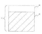
図2は、アパーチャ部材10を半導体レーザ71側から見た拡大図である。図2に示すように、レーザ光を通過させるべき部分は開口し(開口部12)、その外側は遮光されている(遮光部11)。アパーチャ部材10において、遮光部11の表面の少なくとも一部には反射防止構造体14が形成されている。図2では、反射防止構造体14が形成されている部分を斜線で示している。なお、図2では、アパーチャ部材10の表面全体に反射防止構造体14が形成されている場合を図示しているが、必ずしもアパーチャ部材10の表面全体に反射防止構造体14が形成されている必要はなく、表面の少なくとも一部に反射防止構造体が形成されていればよい。
FIG. 2 is an enlarged view of the
図3は、図2に示すアパーチャ部材の遮光部11の断面図である。図3において、アパーチャ部材10は、レーザ光を吸収可能な材料からなる基材13により構成され、当該基材13の表面には、反射防止構造体14が形成されている。
FIG. 3 is a cross-sectional view of the
反射防止構造体14とは、所定の形状を有する構造単位が、レーザ光(アパーチャ部材10で反射して半導体レーザ71へ到達してしまう光)の波長(例えば、780nm)よりも小さいピッチで周期的にアレイ状に配列されたものである。このように所定の形状を有する構造単位を周期的にアレイ状に配列させることによって、レーザ光に対して、見かけ上屈折率を連続的に変化させ、空気層との界面での透過/反射特性の入射角依存性及び波長依存性が少ない反射防止機能面を形成させることができる。
The
なお前記ピッチとは、反射防止構造体14が多数の微細構造単位の二次元的な配列により構成されている場合には、最も密な配列方向におけるピッチを意味する。
In addition, the said pitch means the pitch in the densest arrangement direction, when the
また反射防止構造体14とは、反射を低減すべきレーザ光の反射を防止するために、表面に微細構造が形成された部材を意味し、反射を低減すべき光束を完全に反射させない態様だけではなく、所定波長の反射を低減すべき光束の反射を防止する効果を有する態様も含むものである。
Further, the
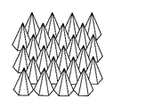
本実施形態に用いることができる反射防止構造体14としては、例えば図4Aの概略拡大図に示すような、高さH1の円錐形状の突起を構造単位とし、これら円錐形状の突起がピッチP1で周期的にアレイ状に配列された構造体があげられる。
As the
構造単位のピッチP1は、反射防止構造体14中、一配列方向において実質上略一定であり、レーザ光の波長よりも小さければよいが、界面での透過/反射特性の入射角依存性及び波長依存性をより一層低減させることができるという点から、かかるピッチP1はレーザ光の波長の1/2以下、さらには1/3以下であることが好ましい。なお例えば後述するような反射防止構造体14の製造性を考慮すると、かかるピッチP1はある程度の大きさを有することが望ましく、通常レーザ光の波長の1/10程度以上であることが好ましい。
The pitch P1 of the structural unit is substantially constant in one arrangement direction in the
また構造単位の高さH1には特に限定がなく、反射防止構造体14中、全ての構造単位の高さH1が必ずしも一定でなくてもよいが、かかる高さH1が高いほど、レーザ光のなかの不要光に対する反射防止機能が向上するという利点がある。したがって該構造単位の高さH1は、少なくとも前記ピッチP1以上(最小の構造単位の高さがピッチ以上)、さらには少なくともピッチP1の3倍以上(最小の構造単位の高さがピッチの3倍以上)であることが好ましい。なおやはり、例えば後述するような反射防止構造体14の製造性を考慮すると、かかる高さH1がある程度の大きさまでであることが望ましく、通常高くともピッチP1の5倍程度以下(最大の構造単位の高さがピッチの5倍程度以下)であることが好ましい。
Further, the height H1 of the structural unit is not particularly limited, and the height H1 of all the structural units in the
本実施形態においては、上述のように、反射防止構造体14として構造単位が例えば円錐形状(図4A)の構造体を用いることができる。例えば、波長780nmのレーザ光を用いる場合、ピッチ0.15μm、高さ0.15μmの円錐形の反射防止構造体14を形成するとよい。
In the present embodiment, as described above, the
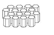
しかしながら、反射防止構造体14の構造は、必ずしも図4Aに示す円錐形の構造体に限定されるものではなく、例えば構造単位が正六角錐形状や、四角錐形状などの角錐形状(図4B)の構造体であってもよい。また、かかる構造単位の形状は必ずしも錐状に限定されるものでもなく、円柱形状(図5A)や角柱形状(図5B)などの柱状であっても、先端が丸くなっている釣鐘状(図6A及び図6B)であっても、円錐台形状(図7A)や角錐台形状(図7B)などの錐台状であってもよい。また、各構造単位は厳密な幾何学的な形状である必要はなく、実質的に錐状、柱状、釣鐘状、錐台状などであればよい。
However, the structure of the
さらに上記図4〜図7では、反射防止構造体14として構造単位が突出形状のものを示しているが、本実施形態においてはこのような突出形状のものに限定されることもなく、例えば平面に錐状、柱状、釣鐘状、錐台状などの陥没形状の構造単位が、レーザ光の波長よりも小さいピッチで周期的にアレイ状に配列するように形成された反射防止構造体14を用いることも可能である。また突出形状の構造単位と陥没形状の構造単位とが1つの反射防止構造体14中に同時に存在していてもよい。なお、かかる突出形状の構造単位と陥没形状の構造単位とが同時に存在した反射防止構造体14の場合、その突出部の高さと陥没部の深さとの合計が前記高さH1の範囲内であることが好ましい。このように、本実施形態に用いられる反射防止構造体14は、各構造単位がレーザ光の波長よりも小さいピッチで周期的にアレイ状に配列され、不要光の反射を充分に防止することができるものであれば、その構造単位の形状などは特に限定されるものではない。
Further, in FIGS. 4 to 7, the
なお本実施形態においては、空気界面でレーザ光の屈折率が連続的に変化し、不要光の反射をより充分に防止することができるという点から、構造単位が略錐状の突出形状及び/または略錐状の陥没形状である反射防止構造体14を用いることが好ましく、略錐状が略正六角錐状である場合には、構造単位が高充填率で配列され、空気界面でレーザ光の屈折率がさらに連続的に変化するといったレーザ光の透過特性がより一層向上するという点から、特に好ましい。
In the present embodiment, the refractive index of the laser light continuously changes at the air interface, and reflection of unnecessary light can be more sufficiently prevented. Alternatively, it is preferable to use the
アパーチャ部材10を構成する、レーザ光を吸収可能な材料としては、通常約780nmの波長のレーザ光を吸収することができる材料であれば特に限定がなく、例えば黒色材料を好適に用いることができる。かかる黒色材料は、例えばポリカーボネート系樹脂、アクリル系樹脂などの樹脂に、シアン、マゼンタ、イエローなどの色素を混合して得られる黒色染料(例えば、Plast Black 8950、Plast Black 8970(いずれも商品名、有本化学工業(株)製))などの染料や、カーボンブラックなどの顔料を含有させることによって得ることができる。
The material constituting the
本実施形態に係るアパーチャ部材10の製造方法にも特に限定がないが、一例として、例えば石英ガラス基板などに電子線描画などの方法でパターンを描画してドライエッチングなどの加工を行い、予め反射防止構造体14と同一形状に精密加工された高精度のマスター型を形成した後、該マスター型を用いて、加熱軟化したガラス材料をプレス成形することによってガラス製の反射防止構造体成形用型を作製し、該反射防止構造体成形用型を用いて、例えば前記黒色材料(黒色樹脂)などのレーザ光を吸収可能な材料をプレス成形に供する方法などがあげられる。かかる方法を採用した場合には、反射防止構造体14をその表面の少なくとも一部に有するアパーチャ部材10を安価でかつ大量に製造することができる。
The manufacturing method of the
また上記の他にも、本実施形態に係るアパーチャ部材10を製造する際には、例えば材料としてアルミニウム、真鍮、ステンレス鋼、銅、その他の合金などの金属を用い、切削加工やプレス成形により製造することも可能であるし、またエッチング、X線リソグラフィ、フォトリソグラフィなどを適宜組み合わせる方法により製造することも可能である。なお、通常半導体レーザ71から出射されるレーザ光の強度は高いため、上述のように、アパーチャ部材10に到達するレーザ光Gもある程度の強度を有する。したがって、アパーチャ部材10の近傍は、比較的高温となる可能性があるので、かかるアパーチャ部材10としては、上記金属などの耐熱性を有する材料からなるものをより好適に用いることができる。
In addition to the above, when the
以下、図1を参照して、以上のように構成された走査光学系の動作について説明する。 Hereinafter, the operation of the scanning optical system configured as described above will be described with reference to FIG.
半導体レーザ71から出射された発散性のレーザ光74は、コリメータレンズ72に入射し、収束性の平行光に変換される。そして、平行光に変換されたレーザ光74は、アパーチャ部材10に入射し、開口部によって光束が制限される。アパーチャ部材10から出射したレーザ光74は、シリンドリカルレンズ73により回転多面鏡75の反射面近傍に主走査方向に延びた線状に結像される。回転多面鏡75は、回転中心軸76を中心として回転し、入射したレーザ光74を偏向走査する。回転多面鏡75により偏向走査されたレーザ光74は、その後、主走査方向について収束性のまま、副走査方向については発散性のレーザ光として走査レンズ8に入射し、走査レンズ8により等速に走査され、被走査面78上にスポットとして結像される。
The
図1では、偏向走査された走査中心でのレーザ光74aと、両走査端でのレーザ光74b及びレーザ光74cとを代表的に示している。アパーチャ部材10は、コリメータレンズ72及びシリンドリカルレンズ73の間に配置され、コリメータレンズ72により略平行光に変換されたレーザ光74は、アパーチャ部材10の開口部12により光束が制限され、その一部のみが開口部12を通過する。アパーチャ部材10が有する開口部12の形状や大きさを調整することにより、感光ドラム78上でのレーザ光74の光スポットの形状及びサイズを最適化することができる。
FIG. 1 representatively shows the
ここで、上述のように、本実施の形態に係るアパーチャ部材10は、レーザ光を吸収可能な材料からなり、アパーチャ部材10の表面には反射防止構造体14が形成されている。これにより、アパーチャ部材10においてレーザ光が到達する面と空気との界面での光の反射を抑制し、かつ、入射したレーザ光を実質的に完全に吸収することができる。したがって、アパーチャ部材10からの反射光が半導体レーザ71へ戻ることを防止し、戻り光による出力変動を抑制することができる。
Here, as described above, the
(第2の実施形態)
以下、本発明の第2の実施形態に係るアパーチャ部材及びそれを用いる走査光学系について、図面を参照しながら説明する。
(Second Embodiment)
Hereinafter, an aperture member and a scanning optical system using the same according to a second embodiment of the present invention will be described with reference to the drawings.
本実施形態に係る走査光学系の基本構成は第1の実施形態と同様であるが、アパーチャ部材10の少なくも一部が有する反射防止構造体14及びレーザ光を吸収可能な材料の構成が第1の実施形態と相違する。
The basic configuration of the scanning optical system according to this embodiment is the same as that of the first embodiment, but the configuration of the
図8は、本実施形態に係る反射防止構造体14及びレーザ光を吸収可能な材料を模式的に示す概略断面図である。図8において、基材13の上に、反射防止構造体14を有するシート21が貼付されている。
FIG. 8 is a schematic cross-sectional view schematically showing the
基材13は、吸収すべき所望の光束を包括する大きさ、機械的強度及び構成上必要な厚みを有する。基材13は、レーザ光を吸収することができる材料であれば特に限定がなく、例えば黒色材料を好適に用いることができる。黒色材料は、第1の実施形態と同様に、ポリカーボネート樹脂、アクリル樹脂等の基材中にシアン、マゼンタ、イエロー等の色素を混ぜることによって得られる黒色染料(例えば、Plast Black 8950、Plast Black 8970(いずれも商品名、有本化学工業(株)製))等の染料や、カーボンブラックなどの顔料を含有させることによって得られる。
The
シート21は、例えば、アクリル樹脂等の透明材料からなり、その表面の少なくとも一部に、レーザ光の波長よりも小さいピッチで形成された反射防止構造体14を有する。シート21の厚みは、ハンドリングが容易で、かつ機械的強度が十分に得ることができればよいが、好ましくは10μm以上であるとよい。
The
反射防止構造体14の高さ及びピッチは、第1の実施形態と同様に決定すればよく、例えば、レーザ光の波長が780nmである場合、シート21上には、例えば図4に示すように、ピッチ0.15μm、高さ0.15μmの円錐型の反射防止構造体14をシート21上に形成するとよい。このように、反射防止構造体14は、半導体レーザ71の波長よりも小さいピッチで、かつ、当該ピッチ以上の高さを有する。
The height and pitch of the
また、シート21と基材13との屈折率の差は、0.2以下である。シート21と基材13の屈折率の差を0.2以下とすることにより、シート21と基材13との界面で発生する反射率を問題とならない程度まで抑えることができる。さらには、シート21と基材13との屈折率の差は、0.1以下であるのが望ましい。シート21と基材13との屈折率の差を0.1以下とすることにより、シート21と基材13との界面で発生する反射率をさらに低減することが可能となり、迷光の発生を効率よく抑えることができる。
Further, the difference in refractive index between the
反射防止構造体14を有するシート21の製造法には特に限定がないが、シート21は、例えば、以下のようにして製造することができる。例えば石英ガラス基板などに電子線描画などの方法でパターンを描画してドライエッチングなどの加工を行い、予め反射防止構造体14と同一形状に精密加工された高精度のマスター型を形成した後、該マスター型を用いて、加熱軟化したガラス材料をプレス成形することによってガラス製の反射防止構造体成形用型を作製し、該反射防止構造体成形用型を用いて、例えば上記アクリル樹脂などの材料をプレス成形に供する方法などがあげられる。かかる方法を採用した場合には、反射防止構造体14を少なくとも一部に有するシート21を安価でかつ大量に製造することができる。
Although the manufacturing method of the
プレス成形に用いるアクリル樹脂は、ハンドリングの容易性及び機械的強度の点から、厚みが10μm以上(シート21の厚み+0.15μm)であることが好ましい。これにより、ハンドリングが容易で、かつ充分な機械的強度を有するシート21を製造することができる。
The acrylic resin used for press molding preferably has a thickness of 10 μm or more (the thickness of the
上記のように、本実施形態によれば、レーザ光を吸収可能な材料からなる基材13の表面に、反射防止構造体14を有するシート21を貼付することによって、入射する不要なレーザ光を、空気との界面での反射を充分に防止し、かつ入射した不要なレーザ光を実質的に完全に吸収することができる。したがって、これにより、目的の構造物に対して、安価かつ簡易に反射防止機能を付与することができる。
As described above, according to the present embodiment, unnecessary laser light incident thereon can be obtained by attaching the
また、本実施形態では、シートの材料はアクリル樹脂であるものとして説明したが、シートの材料はこれに限られず、例えば。ポリカーボネート樹脂や、ポリエチレンテレフタレート樹脂等を用いることもできる。 Further, in the present embodiment, the sheet material is described as being an acrylic resin, but the sheet material is not limited to this, for example. A polycarbonate resin, a polyethylene terephthalate resin, etc. can also be used.
なお、本実施形態においては、シートの材料として透明材料が用いられているが、必ずしも透明材料に限定されるものではなく、レーザ光を吸収可能な材料、例えば、染料や顔料により黒色に着色された黒色材料を用いてもよい。レーザ光を吸収可能な材料からなるシートを用いることにより、レーザ光の吸収効率のさらなる向上を図ることができる。なお、シートがレーザ光を吸収可能な材料からなる場合、シートが貼付される基材は必ずしも吸収可能な材料で構成されている必要はない。 In this embodiment, a transparent material is used as a material for the sheet, but the material is not necessarily limited to the transparent material, and is colored black by a material capable of absorbing laser light, for example, a dye or a pigment. A black material may be used. By using a sheet made of a material that can absorb laser light, the laser light absorption efficiency can be further improved. In addition, when a sheet | seat consists of a material which can absorb a laser beam, the base material to which a sheet | seat is affixed does not necessarily need to be comprised with the material which can absorb.
また、本実施形態では、反射防止構造体として構造単位が例えば円錐形状(図4A)の構造体を用いる場合を例に説明したが、第1の実施形態の場合と同様に、反射防止構造体の構造単位は必ずしもこのような形状の構造体に限定されるものではなく、例えば構造単位が正六角錐形状や、四角錐形状などの角錐形状(図4B)の構造体であってもよい。また、かかる構造単位の形状は必ずしも錐状に限定されるものでもなく、円柱形状(図5A)や角柱形状(図5B)などの柱状であっても、先端が丸くなっている釣鐘状(図6A及び図6B)であっても、円錐台形状(図7A)や角錐台形状(図7B)などの錐台状であってもよい。また、各構造単位は厳密な幾何学的な形状である必要はなく、実質的に錐状、柱状、釣鐘状、錐台状などであればよい。また、第1の実施形態と同様に、反射防止構造体として構造単位は突出形状であってもよく、また、陥没形状であってもよい。 In the present embodiment, the case where a structural unit having a conical shape (for example, FIG. 4A) is used as an example of the antireflection structure has been described as an example. However, as in the case of the first embodiment, the antireflection structure is used. The structural unit is not necessarily limited to such a structure. For example, the structural unit may be a structure having a regular hexagonal pyramid shape or a pyramid shape such as a quadrangular pyramid shape (FIG. 4B). Further, the shape of such a structural unit is not necessarily limited to a cone shape, and a bell shape (FIG. 5A) having a rounded tip even in a columnar shape (FIG. 5A) or a prismatic shape (FIG. 5B). 6A and 6B) may be a truncated cone shape such as a truncated cone shape (FIG. 7A) or a truncated pyramid shape (FIG. 7B). Moreover, each structural unit does not need to be a strict geometric shape, and may be substantially a cone shape, a column shape, a bell shape, a frustum shape, or the like. As in the first embodiment, the structural unit of the antireflection structure may be a protruding shape, or may be a depressed shape.
また、第1及び第2の実施形態では、波長780nmのレーザ光を用いる場合を例に説明したが、勿論レーザ光の波長は780nmに限定されず、これ以外の波長のレーザ光を用いても構わない。レーザ光として、例えば、紫外光(紫外帯域波長:150nm〜400nm)や、可視光(可視帯域波長:400nm〜700nm)、近赤外光(近赤外帯域波長:700nm〜2μm)、遠赤外光(遠赤外帯域波長:2μm〜13μm)を用いることができる。この場合、反射防止構造体のピッチや高さは、それぞれのレーザ光の最短波長に基づいて決定するとよい。例えば、反射防止構造体における構造単位のピッチP1は、それぞれのレーザ光の最短波長よりも小さいピッチで形成されるとよい。また、構造単位の高さH1は、ピッチP1(最小の構造単位の高さがピッチ以上)以上、さらには、少なくともピッチP1の3倍以上(最小の構造単位の高さがピッチの3倍以上)であることが好ましい。 In the first and second embodiments, the case where laser light having a wavelength of 780 nm is used has been described as an example. However, the wavelength of laser light is not limited to 780 nm, and laser light having other wavelengths may be used. I do not care. Examples of laser light include ultraviolet light (ultraviolet band wavelength: 150 nm to 400 nm), visible light (visible band wavelength: 400 nm to 700 nm), near infrared light (near infrared band wavelength: 700 nm to 2 μm), far infrared. Light (far-infrared band wavelength: 2 μm to 13 μm) can be used. In this case, the pitch and height of the antireflection structure may be determined based on the shortest wavelength of each laser beam. For example, the pitch P1 of the structural units in the antireflection structure is preferably formed with a pitch smaller than the shortest wavelength of each laser beam. Further, the height H1 of the structural unit is equal to or greater than the pitch P1 (the minimum structural unit height is equal to or greater than the pitch), and at least three times the pitch P1 (the minimum structural unit height is equal to or greater than three times the pitch) ) Is preferable.
また、第1の実施形態及び第2の実施形態では、アパーチャ部材が走査光学系に適用される場合を例に説明したが、走査光学系に限らず、例えば、光ピックアップ装置に適用されるレーザ光学系に、第1の実施形態または第2の実施形態に係るアパーチャ部材を用いることとしてもよい。 In the first and second embodiments, the case where the aperture member is applied to the scanning optical system has been described as an example. However, the present invention is not limited to the scanning optical system, and for example, a laser applied to an optical pickup device. The aperture member according to the first embodiment or the second embodiment may be used for the optical system.
(第3の実施形態)
図9は、第3の実施形態に係る画像読取装置に適用された走査光学系の光学構成図である。第3の実施形態に係る画像読取装置は、第1の実施形態で説明した走査光学系を画像読取光学系として搭載している。なお、図9において、第3の実施形態に係る画像読取装置の走査光学系は、第1の実施形態に係る走査光学系と概略構成が等しいので、相違点のみを説明する。なお、図9において、同じ符号が付された構成は、第1の実施形態で説明した構成と同一であることを示している。
(Third embodiment)
FIG. 9 is an optical configuration diagram of a scanning optical system applied to the image reading apparatus according to the third embodiment. An image reading apparatus according to the third embodiment includes the scanning optical system described in the first embodiment as an image reading optical system. In FIG. 9, the scanning optical system of the image reading apparatus according to the third embodiment has the same schematic configuration as the scanning optical system according to the first embodiment, so only the differences will be described. Note that in FIG. 9, configurations with the same reference numerals indicate that they are the same as the configurations described in the first embodiment.
第3の実施形態に係る画像読取装置に適用された走査光学系は、第1の実施形態に係る走査光学系に加えて、ハーフミラー101と、検出器102と、検出光学系103とを備えている。ハーフミラー101は、半導体レーザ71からのレーザ光を透過させ、読取るべき2次元画像である読取り面104を照明するとともに、読取り面104からの戻り光を検出光学系103に向けて反射する。検出光学系103は、ハーフミラー101で反射された検出器102に戻り光を導く。第3の実施形態の画像読取装置は、第1の実施形態に係る走査光学系を用いているので、読み取り不良を防止し、高品位の画像を読み取ることができる。なお、第1の実施形態に示した走査光学系に換えて第2の実施形態に係る走査光学系を用いてもよい。
The scanning optical system applied to the image reading apparatus according to the third embodiment includes a
(第4の実施形態)
図10は、本発明の第4の実施の形態における画像形成装置の構成を示す断面図である。この画像形成装置は、外部から入力されるデータ信号に基づいて、モノクロ画像を形成するプリンター装置である。本実施形態に係る画像形成装置は、第1の実施形態に係る走査光学系を露光光学系81として搭載している。
(Fourth embodiment)
FIG. 10 is a cross-sectional view showing a configuration of an image forming apparatus according to the fourth embodiment of the present invention. This image forming apparatus is a printer apparatus that forms a monochrome image based on a data signal input from the outside. The image forming apparatus according to the present embodiment includes the scanning optical system according to the first embodiment as an exposure
図10に示すように、第4の実施形態に係る画像形成装置は、一次帯電器80と、露光光学系81と、現像器82と、転写帯電器83と、クリーナー84と、定着装置85と、給紙カセット86と、感光ドラム87とを備える。以下、図10を用いて動作について説明する。露光光学系81によって、静電潜像が形成され印字情報が静電潜像として感光ドラム87上に書き込まれる。感光ドラム87は、光が照射されると電荷が変化する感光体が表面を覆っている。一次帯電器80によって、感光ドラム87の表面に静電気イオンが付着し帯電する。帯電した感光ドラム87は、現像器82によって、印字部に帯電トナーが付着して現像される。感光ドラム87に付着したトナーは、転写帯電器83によって、給紙カセット86から供給された用紙に転写される。転写されたトナーは、定着装置85によって、用紙に定着される。残ったトナーは、クリーナー84によって除去される。
As shown in FIG. 10, the image forming apparatus according to the fourth embodiment includes a
第4の実施形態の画像形成装置は、第1の実施形態に係る走査光学系を用いているので、感光ドラム87の感光体上を走査するレーザ光の出力を安定させ、かつ場所による濃度むらがない高品質な画像を形成することができる。なお、第1の実施形態に示した走査光学系に換えて、第2の実施形態に係る走査光学系を用いてもよい。
Since the image forming apparatus of the fourth embodiment uses the scanning optical system according to the first embodiment, the output of the laser beam that scans the photosensitive member of the
本発明は、不要なレーザ光の反射を抑制し、かつ不要なレーザ光を実質的に完全に吸収することができるアパーチャ部材、それを備える走査光学系、並びに走査光学系を備える画像読取装置及び画像形成装置等として有用である。 An aperture member capable of suppressing reflection of unnecessary laser light and substantially completely absorbing unnecessary laser light, a scanning optical system including the same, and an image reading apparatus including the scanning optical system, and It is useful as an image forming apparatus.
10 アパーチャ部材
11 遮光部
12 開口部
13 基材
14 反射防止構造体
21 シート
71 半導体レーザ
72 コリメータレンズ
73 シリンドリカルレンズ
74 レーザ光
74a 走査中心におけるレーザ光
74b 走査端におけるレーザ光
74c 走査端におけるレーザ光
75 回転多面鏡
76 回転軸
77 走査レンズ
78 感光ドラム
80 一次帯電器
81 露光光学系
82 現像器
83 転写帯電器
84 クリーナー
85 定着装置
86 給紙カセット
87 感光ドラム
DESCRIPTION OF
Claims (25)
前記レーザ光の光軸に対して垂直な面と、
前記レーザ光の光束を通過させるための開口部とを備え、
前記レーザ光が入射する前記垂直な面の少なくとも一部に、所定の形状を有する構造単位が前記レーザ光の波長よりも小さいピッチで周期的にアレイ状に配列された反射防止構造体が設けられ、
前記反射防止構造体自体、及び前記光学部材の前記反射防止構造体が設けられた部分のうち、少なくとも一方は、前記レーザ光を吸収可能な材料からなることを特徴とする、光学部材。 An optical member provided on the optical path of laser light,
A plane perpendicular to the optical axis of the laser beam;
An opening for allowing the laser beam to pass therethrough,
An antireflection structure in which structural units having a predetermined shape are periodically arranged in an array at a pitch smaller than the wavelength of the laser light is provided on at least a part of the vertical surface on which the laser light is incident. ,
At least one of the antireflection structure itself and a portion of the optical member provided with the antireflection structure is made of a material capable of absorbing the laser beam.
前記光学部材が備える垂直な面のうち、前記レーザ光が入射する面の少なくとも一部に前記シートが貼付されていることを特徴とする、請求項1に記載の光学部材。 The antireflection structure is formed on a sheet;
2. The optical member according to claim 1, wherein the sheet is attached to at least a part of a surface on which the laser beam is incident among vertical surfaces of the optical member.
前記光学部材が備える垂直な面のうち、前記レーザ光が入射する面の少なくとも一部に前記シートが貼付されていることを特徴とする、請求項13に記載のレーザ光学系。 The antireflection structure is formed on a sheet;
The laser optical system according to claim 13, wherein the sheet is attached to at least a part of a surface on which the laser beam is incident among vertical surfaces of the optical member.
Priority Applications (1)
| Application Number | Priority Date | Filing Date | Title |
|---|---|---|---|
| JP2005095925A JP2006276485A (en) | 2005-03-29 | 2005-03-29 | Aperture member, optical scanning system with same, and image-reading device and image-forming apparatus with the optical scanning system |
Applications Claiming Priority (1)
| Application Number | Priority Date | Filing Date | Title |
|---|---|---|---|
| JP2005095925A JP2006276485A (en) | 2005-03-29 | 2005-03-29 | Aperture member, optical scanning system with same, and image-reading device and image-forming apparatus with the optical scanning system |
Publications (2)
| Publication Number | Publication Date |
|---|---|
| JP2006276485A true JP2006276485A (en) | 2006-10-12 |
| JP2006276485A5 JP2006276485A5 (en) | 2008-04-10 |
Family
ID=37211310
Family Applications (1)
| Application Number | Title | Priority Date | Filing Date |
|---|---|---|---|
| JP2005095925A Pending JP2006276485A (en) | 2005-03-29 | 2005-03-29 | Aperture member, optical scanning system with same, and image-reading device and image-forming apparatus with the optical scanning system |
Country Status (1)
| Country | Link |
|---|---|
| JP (1) | JP2006276485A (en) |
Cited By (2)
| Publication number | Priority date | Publication date | Assignee | Title |
|---|---|---|---|---|
| JP2010513961A (en) * | 2006-12-22 | 2010-04-30 | シュライフリング ウント アパラーテバウ ゲゼルシャフト ミット ベシュレンクテル ハフツング | Optical rotary coupler with large return loss |
| JP2010197798A (en) * | 2009-02-26 | 2010-09-09 | Toppan Printing Co Ltd | Optical element having forgery prevention function and forgery prevention display body equipped with the same |
Citations (10)
| Publication number | Priority date | Publication date | Assignee | Title |
|---|---|---|---|---|
| JPS6247832A (en) * | 1985-08-28 | 1987-03-02 | Olympus Optical Co Ltd | Optical head |
| JPH0588096A (en) * | 1991-09-26 | 1993-04-09 | Matsushita Electric Ind Co Ltd | Light beam scanning device |
| JPH0667102A (en) * | 1992-08-24 | 1994-03-11 | Canon Inc | Light emitting optical device |
| JPH06337303A (en) * | 1993-05-31 | 1994-12-06 | Toray Ind Inc | Antireflection plastic optical parts |
| JPH09243945A (en) * | 1996-03-13 | 1997-09-19 | Canon Inc | Optical scanner |
| JP2001272505A (en) * | 2000-03-24 | 2001-10-05 | Japan Science & Technology Corp | Surface treating method |
| JP2001330706A (en) * | 2000-05-19 | 2001-11-30 | Nof Corp | Reflection reducing material and its use |
| JP2003240903A (en) * | 2002-02-20 | 2003-08-27 | Dainippon Printing Co Ltd | Antireflection article |
| JP2004191878A (en) * | 2002-12-13 | 2004-07-08 | Matsushita Electric Ind Co Ltd | Prism system, projection display device using the same, rear projector, and multi-vision system |
| JP2006267623A (en) * | 2005-03-24 | 2006-10-05 | Matsushita Electric Ind Co Ltd | Optical scanner and image reader equipped therewith, and image forming apparatus |
-
2005
- 2005-03-29 JP JP2005095925A patent/JP2006276485A/en active Pending
Patent Citations (10)
| Publication number | Priority date | Publication date | Assignee | Title |
|---|---|---|---|---|
| JPS6247832A (en) * | 1985-08-28 | 1987-03-02 | Olympus Optical Co Ltd | Optical head |
| JPH0588096A (en) * | 1991-09-26 | 1993-04-09 | Matsushita Electric Ind Co Ltd | Light beam scanning device |
| JPH0667102A (en) * | 1992-08-24 | 1994-03-11 | Canon Inc | Light emitting optical device |
| JPH06337303A (en) * | 1993-05-31 | 1994-12-06 | Toray Ind Inc | Antireflection plastic optical parts |
| JPH09243945A (en) * | 1996-03-13 | 1997-09-19 | Canon Inc | Optical scanner |
| JP2001272505A (en) * | 2000-03-24 | 2001-10-05 | Japan Science & Technology Corp | Surface treating method |
| JP2001330706A (en) * | 2000-05-19 | 2001-11-30 | Nof Corp | Reflection reducing material and its use |
| JP2003240903A (en) * | 2002-02-20 | 2003-08-27 | Dainippon Printing Co Ltd | Antireflection article |
| JP2004191878A (en) * | 2002-12-13 | 2004-07-08 | Matsushita Electric Ind Co Ltd | Prism system, projection display device using the same, rear projector, and multi-vision system |
| JP2006267623A (en) * | 2005-03-24 | 2006-10-05 | Matsushita Electric Ind Co Ltd | Optical scanner and image reader equipped therewith, and image forming apparatus |
Cited By (2)
| Publication number | Priority date | Publication date | Assignee | Title |
|---|---|---|---|---|
| JP2010513961A (en) * | 2006-12-22 | 2010-04-30 | シュライフリング ウント アパラーテバウ ゲゼルシャフト ミット ベシュレンクテル ハフツング | Optical rotary coupler with large return loss |
| JP2010197798A (en) * | 2009-02-26 | 2010-09-09 | Toppan Printing Co Ltd | Optical element having forgery prevention function and forgery prevention display body equipped with the same |
Similar Documents
| Publication | Publication Date | Title |
|---|---|---|
| JP4976092B2 (en) | Optical scanning device and image forming apparatus using the same | |
| JP4612842B2 (en) | Optical scanning device | |
| JP5489612B2 (en) | Scanning optical device and image forming apparatus using the same | |
| US6829104B2 (en) | Resin-made non-spherical optical element, optical scanning device using the optical element, and image forming apparatus using the optical scanning device | |
| US20080239060A1 (en) | Image forming apparatus and laser scanning unit and polygon mirror thereof | |
| JP2010002832A (en) | Optical scanning device and image forming apparatus | |
| JP4878905B2 (en) | Optical scanning device, optical writing device, and image forming apparatus | |
| JP2009098332A (en) | Optical scanning device and image forming apparatus using the same | |
| JP4454898B2 (en) | Scanning optical system and image forming apparatus having the same | |
| JP2004109315A (en) | Scanning optical system and image forming apparatus using same | |
| US6496293B2 (en) | Optical scanning device, scanning optical system, optical scanning method and image forming apparatus | |
| JP5316759B2 (en) | Optical scanning device, adjustment method, and image forming apparatus | |
| JP2006267623A (en) | Optical scanner and image reader equipped therewith, and image forming apparatus | |
| JP2006276485A (en) | Aperture member, optical scanning system with same, and image-reading device and image-forming apparatus with the optical scanning system | |
| JP2000249950A (en) | Optical scanner | |
| JP5381258B2 (en) | Exposure apparatus and image forming apparatus | |
| JP2010276860A (en) | Scanning optical system in image forming apparatus | |
| JP4294913B2 (en) | Optical scanning apparatus and image forming apparatus | |
| JP3488432B2 (en) | Multi-beam scanning device, multi-beam scanning method, light source device for multi-beam scanning device and image forming apparatus | |
| JP3242238B2 (en) | Recording device | |
| JP3667236B2 (en) | Scanning optical device and image forming apparatus using the same | |
| JP2021110891A (en) | Optical scanner and image forming apparatus | |
| JP3733294B2 (en) | Scanning optical device and image forming apparatus using the same | |
| JP2008299051A (en) | Optical scanner and image forming apparatus using the same | |
| JP6304476B2 (en) | Optical scanning apparatus and image forming apparatus |
Legal Events
| Date | Code | Title | Description |
|---|---|---|---|
| A521 | Written amendment |
Free format text: JAPANESE INTERMEDIATE CODE: A523 Effective date: 20080221 |
|
| A621 | Written request for application examination |
Free format text: JAPANESE INTERMEDIATE CODE: A621 Effective date: 20080221 |
|
| A977 | Report on retrieval |
Free format text: JAPANESE INTERMEDIATE CODE: A971007 Effective date: 20101015 |
|
| A131 | Notification of reasons for refusal |
Free format text: JAPANESE INTERMEDIATE CODE: A131 Effective date: 20101019 |
|
| A521 | Written amendment |
Free format text: JAPANESE INTERMEDIATE CODE: A523 Effective date: 20101215 |
|
| RD02 | Notification of acceptance of power of attorney |
Free format text: JAPANESE INTERMEDIATE CODE: A7422 Effective date: 20110826 |
|
| A131 | Notification of reasons for refusal |
Free format text: JAPANESE INTERMEDIATE CODE: A131 Effective date: 20110909 |
|
| A02 | Decision of refusal |
Free format text: JAPANESE INTERMEDIATE CODE: A02 Effective date: 20120620 |