JP2006262103A - Volt-ampere converting circuit and error amplifying circuit - Google Patents
Volt-ampere converting circuit and error amplifying circuit Download PDFInfo
- Publication number
- JP2006262103A JP2006262103A JP2005076997A JP2005076997A JP2006262103A JP 2006262103 A JP2006262103 A JP 2006262103A JP 2005076997 A JP2005076997 A JP 2005076997A JP 2005076997 A JP2005076997 A JP 2005076997A JP 2006262103 A JP2006262103 A JP 2006262103A
- Authority
- JP
- Japan
- Prior art keywords
- channel mosfet
- current
- circuit
- voltage
- ratio
- Prior art date
- Legal status (The legal status is an assumption and is not a legal conclusion. Google has not performed a legal analysis and makes no representation as to the accuracy of the status listed.)
- Pending
Links
Images


Abstract
Description
本発明は、電圧電流変換回路およびそれを用いたスイッチング電源の誤差増幅回路に関する。 The present invention relates to a voltage / current conversion circuit and an error amplification circuit of a switching power supply using the voltage / current conversion circuit.
まず、図6によりスイッチング電源の構成例について説明する。図6は入力電圧VDDより出力電圧Voを生成して負荷Zに供給するPWM(パルス幅変調)方式の降圧型DC/DCコンバータである。このDC/DCコンバータは誤差増幅器1,三角波Voscを生成する発振器2,PWMコンパレータ3、スイッチング素子であるPチャネルMOSFET(Metal Oxide Semiconductor Field Effect Transistor)4,同期整流方式の転流素子としてのNチャネルMOSFET5,PWMコンパレータ3の出力に従いPチャネルMOSFET4およびNチャネルMOSFET5を駆動するドライブ回路6,インダクタ7,コンデンサC0,電圧設定用のフィードバック手段となる抵抗R1およびR2,基準電圧VREFを発生する基準電圧源8,並びに出力端子9を有している。10は電源電圧VDDが供給される電源供給ラインである。誤差増幅器1の非反転入力端子には基準電圧VREFが入力され、出力端子と反転入力端子の間には位相補償素子として抵抗RcおよびコンデンサCcが接続されている。PWMコンパレータ3の非反転入力端子には誤差増幅器1の出力信号Verrが入力され、反転入力端子には三角波Voscが入力される。PWMコンパレータ3は誤差増幅器1の出力信号Verrと三角波Voscを比較し、三角波Voscの信号レベルの方が小さければH(ハイレベル)を、三角波Voscの信号レベルの方が大きければL(ローレベル)をPWM信号としてドライブ回路6に出力するものである。PチャネルMOSFET4およびNチャネルMOSFET5のドレインは互いに接続されるとともにインダクタ7の一端に接続されている。またPチャネルMOSFET4およびNチャネルMOSFET5のソースはそれぞれ電源供給ライン10および接地電位(GND)に接続されている。インダクタ7の他端は出力端子9に接続されている。出力端子9とGNDの間にはコンデンサC0および抵抗R1,R2の直列回路が並列に接続されている。抵抗R1とR2の接続点の電位はフィードバック信号VFBとして誤差増幅器1の反転入力端子へ入力される。またDC/DCコンバータの負荷として出力端子9には負荷11が接続されている。
First, a configuration example of the switching power supply will be described with reference to FIG. FIG. 6 shows a PWM (pulse width modulation) step-down DC / DC converter that generates an output voltage Vo from an input voltage VDD and supplies the output voltage Vo to a load Z. This DC / DC converter includes an
以下、簡単にこのDC/DCコンバータの動作を説明する。誤差増幅器1は基準電圧VREFとフィードバック信号VFBの差を増幅した信号VerrをPWMコンパレータ3に入力する。PWMコンパレータ3はVerrと三角波Voscを比較することにより、周期は一定であるが1周期内のHとLの割合が誤差増幅器1の出力により変化する方形波パルス(PWM信号)をドライブ回路6を介してPチャネルMOSFET4のゲートに出力する。すなわち、(VREF−VFB)が大きい(小さい)ほど1周期内のPチャネルMOSFET4がオン(導通)する期間が長く(短く)なるような方形波パルスを発生し、インダクタ7に蓄積するエネルギを大きく(小さく)することにより出力電圧VOを一定に保つ。NチャネルMOSFET5のゲートにも同様に方形波パルスが出力される。基本的にはPチャネルMOSFET4とNチャネルMOSFET5のゲートに出力される方形波パルスは同相であるが、PチャネルMOSFET4とNチャネルMOSFET5が同時にオンして貫通電流が流れることがないように、両方オフの期間であるデッドタイムを設ける。
The operation of this DC / DC converter will be briefly described below. The error amplifier 1 inputs a signal Verr obtained by amplifying the difference between the reference voltage V REF and the feedback signal V FB to the PWM comparator 3. The PWM comparator 3 compares the Verr and the triangular wave Vosc to generate a square wave pulse (PWM signal) whose period is constant but whose ratio of H and L in one period changes according to the output of the
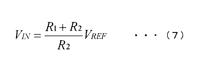
抵抗R1,R2,Rc,コンデンサCc,誤差増幅器1および基準電圧源8は誤差増幅回路を構成する。この部分を抜き出して図7に示す。図7に示す誤差増幅回路は、入力信号VINが入力され、出力信号VOUTを出力する一種の増幅回路である。なお、信号VIN,VOUTはそれぞれ図6のVo,Verrに相当する。図7の誤差増幅回路は、下式の条件を満たすとき直流的に安定する。
Resistors R1, R2, Rc, capacitor Cc,
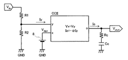
端子数増加の問題に対しては、電流出力型アンプを用いて図8,9の誤差回路を構成するという対策を講ずることができる。すなわち、図8,9の誤差回路であれば外付け端子は1つだけでよい。
図8,9の回路について簡単に説明する。なお、図6,7と同じ部位には同じ記号を付して、当該部位に関する説明は省略する。図8の回路においてOTAはトランスコンダクタンスアンプであり、図中に記したように、入力端子x,yに印加される入力電圧Vx,Vyと出力端子oから出力される出力電流IoがIo=gm(Vx−Vy)という関係を満たすよう機能するものである。なお、gmはコンダクタンスを表す正定数である。図8の回路も、下式の条件を満たすとき直流的に安定する。
To solve the problem of the increase in the number of terminals, it is possible to take a measure of configuring the error circuit of FIGS. 8 and 9 using a current output type amplifier. That is, the error circuit of FIGS. 8 and 9 requires only one external terminal.
The circuits of FIGS. 8 and 9 will be briefly described. The same parts as those in FIGS. 6 and 7 are denoted by the same reference numerals, and description thereof is omitted. In the circuit of FIG. 8, OTA is a transconductance amplifier. As described in the figure, the input voltages Vx and Vy applied to the input terminals x and y and the output current Io output from the output terminal o are Io = g It functions to satisfy the relationship m (Vx−Vy). G m is a positive constant representing conductance. The circuit of FIG. 8 is also stabilized in a direct current when the following equation is satisfied.
電流出力型アンプは上記のように、端子数を減らし、さらにコンデンサCcの容量値を小さくすることができるという長所をもつ反面、過渡応答特性向上のために当該アンプのバイアス電流を増加させると入力オフセット電圧が増加してしまうため、オペアンプ(演算増幅器)を用いた場合に比べて過渡応答特性と低入力オフセット電圧の両立が難しいという問題を有している。
図10に従来の電圧電流変換回路の一例を示す。図10において、12,13はそれぞれ正側および負側の差動入力端子、14は差動回路に一定のバイアス電流を供給するための端子、15は出力端子、トランジスタM31,M33,M35,M38,M39およびM40はPチャネルMOSFET、トランジスタM32,M34,M36およびM37はNチャネルMOSFETである。トランジスタM33,M34,M35,M36およびM39が差動段を構成し、トランジスタM31およびM32が出力段を構成している。トランジスタM40とM39は端子14に流れる電流Ibに比例したバイアス電流を差動段に供給するバイアス回路を構成している。トランジスタM36とM37、トランジスタM38とM31、およびトランジスタM34とM32はそれぞれカレントミラー回路を構成している。
As described above, the current output type amplifier has the advantage that the number of terminals can be reduced and the capacitance value of the capacitor Cc can be reduced. On the other hand, when the bias current of the amplifier is increased to improve the transient response characteristic, Since the offset voltage increases, there is a problem that it is difficult to achieve both transient response characteristics and a low input offset voltage compared to the case where an operational amplifier (operational amplifier) is used.
FIG. 10 shows an example of a conventional voltage-current conversion circuit. In FIG. 10, 12 and 13 are positive and negative differential input terminals, 14 is a terminal for supplying a constant bias current to the differential circuit, 15 is an output terminal, and transistors M31, M33, M35, and M38. , M39 and M40 are P-channel MOSFETs, and transistors M32, M34, M36 and M37 are N-channel MOSFETs. Transistors M33, M34, M35, M36 and M39 form a differential stage, and transistors M31 and M32 form an output stage. The transistors M40 and M39 constitute a bias circuit that supplies a bias current proportional to the current Ib flowing through the terminal 14 to the differential stage. Transistors M36 and M37, transistors M38 and M31, and transistors M34 and M32 form a current mirror circuit, respectively.
一般に、電圧電流変換回路は正負の電流を供給できるようにするために、その出力段が電源(VDD)側から吐出される電流I1と接地(GND)側に流入する電流I2の差を出力電流I0とする回路構成がとられる。図10の回路においても、NチャネルMOSFET・M36に流れる電流を基準としてトランジスタM38とM31によるカレントミラー回路およびトランジスタM36とM37によるカレントミラー回路により電流I1を定め、NチャネルMOSFET・M34に流れる電流を基準としてトランジスタM34とM32によるカレントミラー回路により電流I2を定める構成となっている。通常は入力電圧(差動入力端子12,13からPチャネルMOSFET・M33,M35のゲートにそれぞれ印加される電圧V+およびV−の差電圧)が0のときに、I1=I2となり、I0=0となるよう設計される。
In general, in order for the voltage-current converter circuit to supply positive and negative currents, the difference between the current I1 discharged from the power supply (VDD) side and the current I2 flowing into the ground (GND) side of the output stage is the output current. A circuit configuration of I0 is taken. Also in the circuit of FIG. 10, the current I1 is determined by the current mirror circuit including the transistors M38 and M31 and the current mirror circuit including the transistors M36 and M37 with reference to the current flowing through the N-channel MOSFET M36. As a reference, the current I2 is determined by a current mirror circuit including transistors M34 and M32. Normally, when the input voltage (difference voltage between voltages V + and V− applied from the
上記のようにカレントミラー回路を用いた電圧電流変換回路において、製造プロセスのばらつきによりカレントミラー回路のミラー比(カレントミラー回路に入力される電流と、当該入力電流に応じてカレントミラー回路により生成される出力電流との比)が設計値からずれた場合について考える。この場合は入力電圧が0でも出力電流が0とはならず、オフセット電流Ioffが発生する。見方を変えれば、出力電流を0とするために、−Ioff/gmのオフセット電圧を入力電圧として加える必要がある(gmは電圧電流変換回路の伝達コンダクタンス)。
誤差増幅回路への適用においては上記のオフセット電圧が制御系の直流安定点の誤差に直結するため、オフセット電圧の値を許容範囲内の小さな値に収めなければならない。オフセット電圧を小さくするためにはオフセット電流Ioffの絶対値を低減する必要があり、そのためにバイアス電流Ib自体を小さくしてしまう電圧電流変換回路が提案されている(例えば、特許文献1参照)。
In application to an error amplifying circuit, the offset voltage is directly connected to the error of the DC stable point of the control system, so that the value of the offset voltage must be kept within a small allowable range. In order to reduce the offset voltage, it is necessary to reduce the absolute value of the offset current Ioff. For this reason, a voltage-current conversion circuit that reduces the bias current Ib itself has been proposed (see, for example, Patent Document 1).
特許文献1に示す電圧電流変換回路は、バイアス電流を小さくすればそれに比例してオフセット電流Ioffも小さくなるという考えに基づくものであるが、バイアス電流を小さくすると、以下の不具合が生じる。すなわち、図10に示す回路構造において、全てのカレントミラー回路のミラー比を1:1とすると、電圧電流変換回路としての電流出力範囲は−Ib〜+Ib(入力電圧範囲は−Ib/gm〜+Ib/gm)となる(ミラー比が1:1でない場合は−kIb〜+kIbとなるだけで、以下の議論は同様である。なお、ここでkは正定数。)。そのため、電流出力範囲もしくは入力電圧範囲はバイアス電流Ibを小さくすると狭くなってしまう。これにより、このような電圧電流変換回路を誤差増幅回路に適用する場合、定常状態では出力電流が0なので問題は生じないものの、初期の立ち上がり時や制御系の変化などで大きな信号が入力された場合、出力電流の制限が生じて応答が伝達関数から期待されるものより遅くなってしまうという問題がある。
The voltage-current conversion circuit shown in
本発明は上記の点に鑑みてなされたものであり、その目的は上記の課題を解決して、入力オフセット電圧が小さく、かつ出力電流範囲の広い電圧電流変換回路を提供することにある。さらに、当該電圧電流変換回路を用いた、低入力オフセット電圧と高速過渡応答を両立させた電流出力型誤差増幅回路を提供することを目的とする。 The present invention has been made in view of the above points, and an object of the present invention is to solve the above-described problems and provide a voltage-current conversion circuit having a small input offset voltage and a wide output current range. It is another object of the present invention to provide a current output type error amplifying circuit using the voltage-current conversion circuit and having both a low input offset voltage and a fast transient response.
そこで、上記課題を解決するために、請求項1に係る発明は、第1および第2の入力端子,出力端子,第1のカレントミラーを構成する第1のPチャネルMOSFETおよび第2のPチャネルMOSFET,第2のカレントミラーを構成する第1のNチャネルMOSFETおよび第2のNチャネルMOSFET,演算増幅器,バイアス電圧発生手段,並びに第1の抵抗を有し、前記第1のPチャネルMOSFETに流れる電流に対する前記第2のPチャネルMOSFETに流れる電流の比が前記第1のNチャネルMOSFETに流れる電流に対する前記第2のNチャネルMOSFETに流れる電流の比に等しくなるよう設定され、前記第1の入力端子と前記入力抵抗の一端が接続され、前記入力抵抗の他端,前記第1のPチャネルMOSFETのドレイン,前記第1のNチャネルMOSFETのドレインおよび前記演算増幅器の非反転入力が接続され、前記第2の入力端子と前記演算増幅器の反転入力が接続され、前記出力端子,前記第2のPチャネルMOSFETのドレインおよび前記第2のNチャネルMOSFETのドレインが接続され、前記演算増幅器の出力端子が前記第1のNチャネルMOSFETおよび前記第2のNチャネルMOSFETのゲートに接続され、前記バイアス電圧発生手段が前記演算増幅器の出力端子と前記第1のNチャネルMOSFETのゲートおよび前記第2のNチャネルMOSFETのゲートとの接続点の間に接続されてなる電圧電流変換回路であることを特徴とする。
In order to solve the above-described problem, the invention according to
請求項2に係る発明は、請求項1に係る発明において、前記バイアス発生手段が、一端が前記演算増幅器の出力端子に接続され、他端が定電流源に接続された第2の抵抗であることを特徴とする。
請求項3に係る発明は、請求項2に係る発明において、電源と基準電位の間にゲート端子とドレイン端子を接続した第3のPチャネルMOSFET,第3の抵抗およびゲート端子とドレイン端子を接続した第3のNチャネルMOSFETを直列に接続して電流生成回路を構成し、該電生成回路に流れる電流に対する前記定電流源に流れる電流の比と前記第2の抵抗の抵抗値に対する前記第3の抵抗の抵抗値の比とが等しくなるよう設定され、MOSFETのゲート幅Wとゲート長Lの比であるW/L比に関し、前記第2のPチャネルMOSFETのW/L比に対する前記第2のNチャネルMOSFETのW/L比の比と前記第3のPチャネルMOSFETのW/L比に対する前記第3のNチャネルMOSFETのW/L比の比が等しく設定されていることを特徴とする。
The invention according to
The invention according to claim 3 is the invention according to
請求項4に係る発明は、請求項3に係る発明のおいて、前記第2のPチャネルMOSFETのゲート長と前記第3のPチャネルMOSFETのゲート長が等しく、前記第2のNチャネルMOSFETのゲート長と前記第3のNチャネルMOSFETのゲート長が等しいことを特徴とする。
請求項5に係る発明は、請求項3または4に係る発明のおいて、前記第2のPチャネルMOSFETと前記第3のPチャネルMOSFETが同じゲート幅とゲート長を有する単位PチャネルMOSFETをそれぞれ一つまたは複数並列に接続して構成され、前記第2のNチャネルMOSFETと前記第3のNチャネルMOSFETが同じゲート幅とゲート長を有する単位NチャネルMOSFETをそれぞれ一つまたは複数並列に接続して構成されていることを特徴とする。
The invention according to
The invention according to
請求項6に係る発明は、請求項1ないし5のいずれかの発明に係る電圧電流変換回路の前記出力端子に容量性素子を接続して構成した誤差増幅回路であることを特徴とする。
請求項7に係る発明は、請求項6に係る発明において、前記容量性素子が前記出力端子と基準電位の間に直列に接続された第4の抵抗およびコンデンサであることを特徴とする。
The invention according to
The invention according to claim 7 is the invention according to
この発明に係る電圧電流変換回路は、出力段を第1のカレントミラー回路により電源(VDD)側から吐出される電流I1と、第2のカレントミラー回路により接地(GND)側に流入する電流I2の差を出力電流I0とする回路構成とし、第1および第2のカレントミラーを構成するトランジスタのゲートを電圧モードで動作する前記オペアンプにより制御するようにしたので、低オフセット電圧と広出力電流範囲を両立させることができる。また、当該電圧電流変換回路の出力端子に容量性素子を接続することにより、低入力オフセット電圧と高速過渡応答を両立させた電流出力型誤差増幅回路を容易に実現することができる。なお、第1のカレントミラーの入力部,第2のカレントミラーの入力部および当該電圧電流変換回路の第1の入力端子と一端が接続された抵抗の他端がオペアンプの非反転入力端子に接続され、電圧電流変換回路の第2の入力端子がオペアンプの反転入力端子に接続されて、オペアンプの反転入力端子と非反転入力端子が仮想短絡するようになっている。 In the voltage-current converter according to the present invention, the current I1 discharged from the power supply (VDD) side by the first current mirror circuit at the output stage and the current I2 flowing into the ground (GND) side by the second current mirror circuit And the gate of the transistors constituting the first and second current mirrors is controlled by the operational amplifier operating in the voltage mode, so that a low offset voltage and a wide output current range are obtained. Can be made compatible. In addition, by connecting a capacitive element to the output terminal of the voltage-current converter circuit, a current output type error amplifier circuit that achieves both a low input offset voltage and a high-speed transient response can be easily realized. The first current mirror input section, the second current mirror input section, and the other end of the resistor connected to the first input terminal of the voltage-current converter circuit are connected to the non-inverting input terminal of the operational amplifier. Then, the second input terminal of the voltage-current conversion circuit is connected to the inverting input terminal of the operational amplifier, and the inverting input terminal and the non-inverting input terminal of the operational amplifier are virtually short-circuited.
以下、本発明の実施の形態について、図面を参照して説明を行う。
図1は本発明に係る電圧電流変換回路の基本構成および動作原理を説明するための図である。図1においてトランジスタM1,M3はPチャネルMOSFETで、それぞれのソース端子が電源VDDに接続され、互いのゲート端子が共通接続されて第1のカレントミラー回路を構成している。第1のカレントミラー回路のミラー比をαとする。トランジスタM2,M4はNチャネルMOSFETで、それぞれのソース端子が接地電位(GND)に接続され、互いのゲート端子が共通接続されて第2のカレントミラー回路を構成している。第2のカレントミラー回路のミラー比も第1のカレントミラー回路のミラー比と同じαにする。トランジスタM1およびM2のドレイン端子は出力端子に接続され、トランジスタM3およびM4のドレイン端子は節点XでオペアンプOPの非反転入力端子に接続されている。また、オペアンプOPの非反転入力端子は、入力抵抗R0を介して第1の入力端子Vinにも接続されている。オペアンプOPの反転入力端子には第2の入力端子Vrefが接続されている。トランジスタM2,M4の両ゲートの共通接続部YはオペアンプOPの出力端子に接続され、トランジスタM1,M3の両ゲートの共通接続部Zは定電圧源Vlsを介してオペアンプOPの出力端子に接続されている。
Hereinafter, embodiments of the present invention will be described with reference to the drawings.
FIG. 1 is a diagram for explaining the basic configuration and operating principle of a voltage-current converter circuit according to the present invention. In FIG. 1, transistors M1 and M3 are P-channel MOSFETs, each of which has a source terminal connected to a power supply VDD and a gate terminal of each other connected in common to form a first current mirror circuit. Let the mirror ratio of the first current mirror circuit be α. The transistors M2 and M4 are N-channel MOSFETs, and their source terminals are connected to the ground potential (GND), and their gate terminals are commonly connected to form a second current mirror circuit. The mirror ratio of the second current mirror circuit is also set to the same α as the mirror ratio of the first current mirror circuit. The drain terminals of the transistors M1 and M2 are connected to the output terminal, and the drain terminals of the transistors M3 and M4 are connected to the non-inverting input terminal of the operational amplifier OP at the node X. The non-inverting input terminal of the operational amplifier OP is also connected to the first input terminal Vin via the input resistor R0. A second input terminal Vref is connected to the inverting input terminal of the operational amplifier OP. The common connection Y of both gates of the transistors M2 and M4 is connected to the output terminal of the operational amplifier OP, and the common connection Z of both gates of the transistors M1 and M3 is connected to the output terminal of the operational amplifier OP via the constant voltage source Vls. ing.
ここで、第1および第2の入力端子Vin,Vrefに入力される電圧もVin,Vrefとし、また、定電圧源Vlsの発生する電圧もVlsとする。定電圧源Vlsは接続部Zの電位を接続部Yの電位に対し電圧Vlsだけレベルシフトするもので、電圧Vlsはレベルシフト電圧となる。オペアンプOPの動作によりオペアンプOPの反転入力端子と非反転入力端子は仮想短絡されて節点Xの電位はVrefに等しくなり、入力端子Vinから入力抵抗R0に流れる電流Iinは(Vin−Vref)/R0となる。なお、R0は入力抵抗R0の抵抗値である。またトランジスタM1,M3のドレイン端子から流れ出す電流をそれぞれI1,I3、トランジスタM2,M4に流れ込む電流をそれぞれI2,I4、出力端子OUTに流れ出す電流をIoutとすると、Iin=I4−I3,I1=I2+Ioutとなる。これと、I1=αI3およびI2=αI4という関係式より、次式が導かれる。 Here, the voltages input to the first and second input terminals Vin and Vref are also Vin and Vref, and the voltage generated by the constant voltage source Vls is Vls. The constant voltage source Vls shifts the potential of the connection part Z by the voltage Vls with respect to the potential of the connection part Y, and the voltage Vls becomes a level shift voltage. By the operation of the operational amplifier OP, the inverting input terminal and the non-inverting input terminal of the operational amplifier OP are virtually short-circuited so that the potential of the node X becomes equal to Vref, and the current Iin flowing from the input terminal Vin to the input resistor R0 is (Vin−Vref) / R. 0 . R 0 is the resistance value of the input resistor R 0 . Further, assuming that currents flowing out from the drain terminals of the transistors M1 and M3 are I1 and I3, currents flowing into the transistors M2 and M4 are I2 and I4, respectively, and current flowing out to the output terminal OUT is Iout, Iin = I4−I3, I1 = I2 + Iout It becomes. From this and the relational expression I1 = αI3 and I2 = αI4, the following equation is derived.
[数10]
Iout=I1−I2=−α(−I3+I4)=−αIin ・・・(10)
電源VDDから供給される電源電圧をVDDとし、接続部Y,Zの電位をそれぞれVy,Vzとすると、電流I3はVDD−Vzの関数であり、電流I4はVyの関数となる。これと、上述のIin=I4−I3およびVz=Vy+Vlsという関係式を満たすようにVy,Vz,I3,I4が定まる。ここでVlsを小さくすると、VDD−VzおよびVyが大きくなり、Iin=I4−I3を満たしつつI3とI4の絶対値が大きくなる。また、Vlsを大きくすると、VDD−VzおよびVyが小さくなり、Iin=I4−I3を満たしつつI3とI4の絶対値が小さくなる。電圧Vlsを十分大きな値にすれば、Iin=Iout=0のときにトランジスタM1〜M4に流れる電流、すなわち出力段を貫通する電流を0にすることも可能であり、この場合は第1および第2のカレントミラー回路のミラー比間にずれが生じても、オフセット電流は生じないことになる。但し、この条件では、Iout=0の近傍における入力電圧Vinの変化に対し接続部YおよびZの電位が大きく変化してしまうため、オペアンプの特性が理想的ではない場合には、歪や過渡応答の悪化を防止するために微小な電流を流しておく方がよい。
[Equation 10]
Iout = I1−I2 = −α (−I3 + I4) = − αIin (10)
Assuming that the power supply voltage supplied from the power supply VDD is VDD and the potentials of the connecting portions Y and Z are Vy and Vz, respectively, the current I3 is a function of VDD-Vz, and the current I4 is a function of Vy. Vy, Vz, I3, and I4 are determined so as to satisfy the relational expressions of Iin = I4-I3 and Vz = Vy + Vls. If Vls is reduced here, VDD-Vz and Vy increase, and the absolute values of I3 and I4 increase while satisfying Iin = I4-I3. When Vls is increased, VDD−Vz and Vy are decreased, and the absolute values of I3 and I4 are decreased while satisfying Iin = I4−I3. If the voltage Vls is set to a sufficiently large value, the current flowing through the transistors M1 to M4 when Iin = Iout = 0, that is, the current passing through the output stage can be set to 0. In this case, the first and first Even if a deviation occurs between the mirror ratios of the two current mirror circuits, no offset current is generated. However, under this condition, the potentials of the connection portions Y and Z greatly change with respect to the change of the input voltage Vin in the vicinity of Iout = 0. Therefore, if the characteristics of the operational amplifier are not ideal, distortion and transient response It is better to pass a minute current in order to prevent the deterioration.
定電圧源Vlsは抵抗を用いて構成することができる。その実施例を図2に示す。図2において、入力端子IN+,IN−はそれぞれオペアンプの非反転入力端子および反転入力端子であり、トランジスタM21,M22,M23,M24およびM25はPチャネルMOSFET、トランジスタM26,M27およびM28はNチャネルMOSFETである。入力端子IN+,IN−、定電流源Ib,トランジスタM21,M22,M24,M25,M26,M27,M28,抵抗Rc2およびコンデンサCc2は図1のオペアンプOPに相当し、定電流源IbおよびトランジスタM21,M22がオペアンプOPのバイアス回路を構成し、入力端子IN+,IN−およびトランジスタM22,M24,M25,M26,M27が差動段を構成し、トランジスタM28,抵抗Rc2およびコンデンサCc2が出力段を構成している。抵抗Rc2およびコンデンサCc2はオペアンプOP自体の位相補償素子である。バイアス回路のトランジスタM21およびM22はそのゲート端子を共通接続してミラー回路を構成して定電流源Ibによって定められる定電流を流すようになっているが、トランジスタM23のゲート端子もトランジスタM21,M22のゲート端子と共通接続することによりトランジスタM23が抵抗Rlsに定電流を供給する構成となっている。定電流源Ibの供給する定電流値もIbとし、トランジスタM21,M23により構成されるカレントミラー回路のミラー比をAとすると、抵抗Rlsにより、Vls=A・Rls・Ibというレベルシフト電圧を生成することができる。 The constant voltage source Vls can be configured using a resistor. An example thereof is shown in FIG. In FIG. 2, input terminals IN + and IN− are a non-inverting input terminal and an inverting input terminal of an operational amplifier, respectively, transistors M21, M22, M23, M24 and M25 are P-channel MOSFETs, and transistors M26, M27 and M28 are N-channel MOSFETs. It is. Input terminals IN +, IN−, constant current source Ib, transistors M21, M22, M24, M25, M26, M27, M28, resistor Rc2 and capacitor Cc2 correspond to the operational amplifier OP of FIG. 1, and constant current source Ib and transistor M21, M22 constitutes a bias circuit of the operational amplifier OP, input terminals IN + and IN− and transistors M22, M24, M25, M26 and M27 constitute a differential stage, and a transistor M28, a resistor Rc2 and a capacitor Cc2 constitute an output stage. ing. The resistor Rc2 and the capacitor Cc2 are phase compensation elements of the operational amplifier OP itself. The transistors M21 and M22 of the bias circuit are connected in common with each other to form a mirror circuit so that a constant current determined by the constant current source Ib flows, but the gate terminal of the transistor M23 is also a transistor M21, M22. The transistor M23 is configured to supply a constant current to the resistor Rls by being commonly connected to the gate terminal. If the constant current value supplied from the constant current source Ib is also Ib, and the mirror ratio of the current mirror circuit composed of the transistors M21 and M23 is A, a level shift voltage of Vls = A · Rls · Ib is generated by the resistor Rls. can do.
図3に図1に示す回路の動作特性を示す。回路パラメータR0,αの値をそれぞれ1MΩおよび0.2としたときの、入力電圧(Vin−Vref)と電流I1,I2およびI0の関係を示している。図3(a)はVlsを大きくした場合の特性であり、図3(b)は逆にVlsを小さくした場合の特性である。
上記のように、本発明は、レベルシフト電圧Vlsの作用により出力電流Iout=0の近傍におけるトランジスタM1〜M4のソース・ゲート間電圧が大きくならないよう抑制され、トランジスタM1〜M4に流れる電流を絞ることができる。すなわち、トランジスタM1〜M4で生じる入力オフセット電圧を低減することができる。また、出力電流Ioutが0近傍ではない場合は、トランジスタM1およびM3又はトランジスタM2およびM4のソース・ゲート間電圧が大きくなって当該トランジスタに流れる電流を大きくすることができ、図10に示す従来の電圧電流変換回路のように電流出力範囲を犠牲にする必要がない。なお、オペアンプOP自体の入力オフセット電圧はそのまま電圧電流変換回路としての入力オフセット電圧となってしまうが、その入力オフセット電圧の値は電流出力型アンプのものに比べて充分小さいので問題はない。
FIG. 3 shows the operating characteristics of the circuit shown in FIG. The relationship between the input voltage (Vin−Vref) and the currents I1, I2 and I0 when the values of the circuit parameters R 0 and α are 1 MΩ and 0.2, respectively, is shown. FIG. 3A shows the characteristics when Vls is increased, and FIG. 3B shows the characteristics when Vls is decreased.
As described above, according to the present invention, the source-gate voltage of the transistors M1 to M4 in the vicinity of the output current Iout = 0 is suppressed by the action of the level shift voltage Vls so that the current flowing through the transistors M1 to M4 is reduced. be able to. That is, the input offset voltage generated in the transistors M1 to M4 can be reduced. Further, when the output current Iout is not near 0, the source-gate voltage of the transistors M1 and M3 or the transistors M2 and M4 can be increased, and the current flowing through the transistor can be increased. There is no need to sacrifice the current output range as in the voltage-current converter circuit. The input offset voltage of the operational amplifier OP itself becomes the input offset voltage as the voltage-current conversion circuit as it is, but there is no problem because the value of the input offset voltage is sufficiently smaller than that of the current output type amplifier.
なお、本発明に係る電圧電流変換回路を用いて誤差増幅回路を構成する場合、上記のように出力電流Iout=0の近傍におけるトランジスタM1〜M4に流れる電流を小さくすることにより比較的高い直流利得を得ることができるが、さらに高い直流利得を得るために、必要に応じてトランジスタM1〜M4としてカスコード接続したMOSFETを適用してもよい。
次に、図4により、本発明に係る電圧電流変換回路を用いた誤差増幅回路の実施例について、説明する。また、図4に示す回路の各回路素子のパラメータ値例を図5に示す。図4において、図1,2,8,9と同じ部位には同じ記号を付して、その詳細な説明は省略する。この誤差増幅回路は、時定数τ=CC・R1/α=50μsを実現するもので、直流安定点はVin=2Vref(この値は可変抵抗R2により変更もしくは調整可能)としてある。ここでは、高抵抗のポリシリコンが使用可能なCMOSプロセスを使用し、全ての回路素子が集積回路に内蔵されることを想定している。
When the error amplifier circuit is configured using the voltage-current converter circuit according to the present invention, a relatively high DC gain is obtained by reducing the current flowing through the transistors M1 to M4 in the vicinity of the output current Iout = 0 as described above. However, in order to obtain a higher DC gain, a cascode-connected MOSFET may be applied as the transistors M1 to M4 as necessary.
Next, an embodiment of an error amplifying circuit using the voltage-current converter circuit according to the present invention will be described with reference to FIG. FIG. 5 shows an example of parameter values of each circuit element of the circuit shown in FIG. 4, the same parts as those in FIGS. 1, 2, 8, and 9 are denoted by the same reference numerals, and detailed description thereof is omitted. This error amplifying circuit realizes a time constant τ = C C · R 1 / α = 50 μs, and the DC stable point is Vin = 2Vref (this value can be changed or adjusted by the variable resistor R2). Here, it is assumed that a CMOS process capable of using high-resistance polysilicon is used, and all circuit elements are built in the integrated circuit.
図4において、トランジスタM10はPチャネルMOSFETであり、トランジスタM11,M12はNチャネルMOSFETである。トランジスタM10とM12のドレインおよびゲートは抵抗R10を介して接続されている。また、トランジスタM11とトランジスタM12のゲートが互いに接続されていて、トランジスタM11とM12はカレントミラー回路を構成している。トランジスタM10,M11,M12および抵抗R10はバイアス電流生成回路を構成していて、電源電圧VDD,抵抗R10およびトランジスタM10,M11の特性により定まる電流IbをM11,M12によるカレントミラー回路で折り返して、次段のオペアンプ+レベルシフト回路にバイアス電流Ibを供給するものであり、図2の回路における定電流源Ibに相当する(図5から分るように、M11,M12からなるカレントミラー回路のミラー比は1である)。 In FIG. 4, the transistor M10 is a P-channel MOSFET, and the transistors M11 and M12 are N-channel MOSFETs. The drains and gates of the transistors M10 and M12 are connected via a resistor R10. The gates of the transistors M11 and M12 are connected to each other, and the transistors M11 and M12 constitute a current mirror circuit. The transistors M10, M11, M12 and the resistor R10 constitute a bias current generating circuit. The current Ib determined by the characteristics of the power supply voltage VDD, the resistor R10, and the transistors M10, M11 is folded by the current mirror circuit of M11, M12, and the next The bias current Ib is supplied to the operational amplifier of the stage + the level shift circuit and corresponds to the constant current source Ib in the circuit of FIG. 2 (as can be seen from FIG. 5, the mirror ratio of the current mirror circuit composed of M11 and M12) Is 1).
トランジスタM21〜M28、抵抗Rls1,Rls2およびコンデンサCcからなるオペアンプ+レベルシフト回路は、定電流源Ibを除く図2の回路とほとんど同じであるが、図2の抵抗Rc2を削除したことと、図2の抵抗Rlsを二つの抵抗Rls1,Rls2に分割し、コンデンサCc2の一端を抵抗Rls1とRls2との接続部に接続したことが異なる。この場合、抵抗Rls1が位相補償抵抗Rc2の機能も担っている。変換回路コアを構成するトランジスタM1〜M4は図1に示すものと同じである。抵抗R1,R2,RcおよびコンデンサCcは図6や図8,9に示すものと同じである。但し、抵抗R2は可変抵抗として、上述のように変更もしくは調整ができるようにしてある。本実施例は、図9の回路に対し、低オフセット電圧と広出力電流範囲を両立させることができる新たなCCIIをバイアス電流生成回路,オペアンプ+レベルシフト回路および変換回路コアという構成により提供するものであり、全体動作については図9と同様になるため説明は省略する。 The operational amplifier + level shift circuit including the transistors M21 to M28, the resistors Rls1 and Rls2, and the capacitor Cc is almost the same as the circuit of FIG. 2 except for the constant current source Ib, but the resistor Rc2 of FIG. The difference is that the two resistors Rls are divided into two resistors Rls1 and Rls2, and one end of the capacitor Cc2 is connected to the connection between the resistors Rls1 and Rls2. In this case, the resistor Rls1 also functions as the phase compensation resistor Rc2. The transistors M1 to M4 constituting the conversion circuit core are the same as those shown in FIG. The resistors R1, R2, Rc and the capacitor Cc are the same as those shown in FIGS. However, the resistor R2 is a variable resistor and can be changed or adjusted as described above. The present embodiment provides a new CCII that can achieve both a low offset voltage and a wide output current range with the configuration of a bias current generation circuit, an operational amplifier + level shift circuit, and a conversion circuit core, compared to the circuit of FIG. The overall operation is the same as in FIG.
図4に示す実施例は、トランジスタM1,M2で構成される出力段から出力される電圧電流変換回路の出力電流が0のときに、出力段に流れる電流がデバイス特性の変化により桁違いに変動することを防ぐ工夫がなされている。その詳細は以下のとおりである。
まず、カレントミラーを構成するトランジスタの特性が揃っていれば(これは集積回路では充分期待できるものである)、図5から分るようにトランジスタM21,M23からなるカレントミラー回路のミラー比は10であるから抵抗Rls1,Rls2に流れる電流は10Ibとなり、抵抗R10(1MΩ)とRls1(30kΩ),Rls2(70kΩ)の直列抵抗の抵抗比は1:10であるから、抵抗R10の両端電圧とRls1,Rls2の直列抵抗の両端電圧(すなわちトランジスタM1のゲートとトランジスタM2のゲートの電位差)は等しくなる。図5から分るように、トランジスタM10とトランジスタM1は同じ単位PチャンネルMOSFET(W(ゲート幅)/L(ゲート長)=8μm/4μm)により構成され、トランジスタM11とトランジスタM2は同じ単位NチャンネルMOSFET(W/L=6μm/4μm)により構成され、トランジスタM10とトランジスタM1の単位トランジスタ数比(40:1)がトランジスタM11とトランジスタM2の単位トランジスタ数比(40:1)と等しいから(言い換えれば、トランジスタM10,M11の単位トランジスタ数比(1:1)がトランジスタM1,M2の単位トランジスタ数比(1:1)に等しいから)、電圧電流変換回路の出力電流が0のときは、トランジスタM10とM1のゲート電圧およびトランジスタM11とM2のゲート電圧がそれぞれ等しくなる。そして、上記の単位トランジスタ数比より、トランジスタM1,M2に流れる電流はトランジスタM10,M11に流れる電流の1/40となる。上述のようにトランジスタM10,M11に流れる電流Ibは電源電圧VDD,抵抗R10およびトランジスタM10,M11の特性により定まるが、ある程度電源電圧VDDが高ければ、抵抗R10に印加される電圧が大きくなって電流Ibを決定する主要因が抵抗R10となるから、MOSFETの特性変動の影響を緩和できる。プロセスによっては、抵抗の温度特性を利用してMOSFETの温度による特性変動を相殺することも可能である。
In the embodiment shown in FIG. 4, when the output current of the voltage-current converter circuit output from the output stage constituted by the transistors M1 and M2 is 0, the current flowing through the output stage varies by orders of magnitude due to changes in device characteristics. The device which prevents doing is made. The details are as follows.
First, if the characteristics of the transistors constituting the current mirror are uniform (this can be fully expected in an integrated circuit), the mirror ratio of the current mirror circuit composed of the transistors M21 and M23 is 10 as can be seen from FIG. Therefore, the current flowing through the resistors Rls1 and Rls2 is 10 Ib, and the resistance ratio of the series resistors of the resistors R10 (1 MΩ), Rls1 (30 kΩ), and Rls2 (70 kΩ) is 1:10. Therefore, the voltage across the resistor R10 and Rls1 , Rls2 has equal voltage across the series resistance (that is, the potential difference between the gate of the transistor M1 and the gate of the transistor M2). As can be seen from FIG. 5, the transistor M10 and the transistor M1 are configured by the same unit P-channel MOSFET (W (gate width) / L (gate length) = 8 μm / 4 μm), and the transistor M11 and the transistor M2 are the same unit N channel. It is constituted by a MOSFET (W / L = 6 μm / 4 μm), and the unit transistor number ratio (40: 1) between the transistors M10 and M1 is equal to the unit transistor number ratio (40: 1) between the transistors M11 and M2 (in other words, (For example, the unit transistor number ratio (1: 1) of the transistors M10 and M11 is equal to the unit transistor number ratio (1: 1) of the transistors M1 and M2), and the output current of the voltage-current conversion circuit is 0. M10 and M1 gate voltage and transistor M11 The gate voltage of M2 becomes equal to each other. From the unit transistor number ratio, the current flowing through the transistors M1 and M2 is 1/40 of the current flowing through the transistors M10 and M11. As described above, the current Ib flowing through the transistors M10 and M11 is determined by the characteristics of the power supply voltage VDD, the resistor R10 and the transistors M10 and M11. If the power supply voltage VDD is high to some extent, the voltage applied to the resistor R10 increases. Since the main factor that determines Ib is the resistor R10, the influence of fluctuations in MOSFET characteristics can be mitigated. Depending on the process, it is possible to cancel the characteristic variation due to the temperature of the MOSFET by utilizing the temperature characteristic of the resistor.
M1,M1,M10,M21〜M25 PチャネルMOSFET
M2,M4,M11,M12,M26〜M28 NチャネルMOSFET
R0,R1,R2,R3,R10,Rls,Rls1,Rls2 抵抗
OP オペアンプ
VDD 電源(電源電圧)
VIN 入力端子(入力電圧)
VOUT 出力端子(出力電圧)
Vref 入力端子(基準電圧)
Vls 定電圧源(レベルシフト電圧)
M1, M1, M10, M21 to M25 P-channel MOSFET
M2, M4, M11, M12, M26 to M28 N-channel MOSFET
R0, R1, R2, R3, R10, Rls, Rls1, Rls2 Resistance OP Operational amplifier VDD Power supply (Power supply voltage)
VIN input terminal (input voltage)
VOUT output terminal (output voltage)
Vref input terminal (reference voltage)
Vls constant voltage source (level shift voltage)
Claims (7)
前記第1のPチャネルMOSFETに流れる電流に対する前記第2のPチャネルMOSFETに流れる電流の比が前記第1のNチャネルMOSFETに流れる電流に対する前記第2のNチャネルMOSFETに流れる電流の比に等しくなるよう設定され、前記第1の入力端子と前記入力抵抗の一端が接続され、前記入力抵抗の他端,前記第1のPチャネルMOSFETのドレイン,前記第1のNチャネルMOSFETのドレインおよび前記演算増幅器の非反転入力が接続され、前記第2の入力端子と前記演算増幅器の反転入力が接続され、前記出力端子,前記第2のPチャネルMOSFETのドレインおよび前記第2のNチャネルMOSFETのドレインが接続され、前記演算増幅器の出力端子が前記第1のNチャネルMOSFETおよび前記第2のNチャネルMOSFETのゲートに接続され、前記バイアス電圧発生手段が前記演算増幅器の出力端子と前記第1のNチャネルMOSFETのゲートおよび前記第2のNチャネルMOSFETのゲートとの接続点の間に接続されていることを特徴とする電圧電流変換回路。 The first and second input terminals, the output terminal, the first P-channel MOSFET and the second P-channel MOSFET constituting the first current mirror, the first N-channel MOSFET constituting the second current mirror, and the first Two N-channel MOSFETs, an operational amplifier, bias voltage generating means, and a first resistor,
The ratio of the current flowing through the second P-channel MOSFET to the current flowing through the first P-channel MOSFET is equal to the ratio of the current flowing through the second N-channel MOSFET to the current flowing through the first N-channel MOSFET. The first input terminal and one end of the input resistor are connected, the other end of the input resistor, the drain of the first P-channel MOSFET, the drain of the first N-channel MOSFET, and the operational amplifier And the second input terminal and the inverting input of the operational amplifier are connected, and the output terminal, the drain of the second P-channel MOSFET, and the drain of the second N-channel MOSFET are connected. And the output terminal of the operational amplifier is connected to the first N-channel MOSFET and the Connected to the gate of the second N-channel MOSFET, and the bias voltage generating means is connected between a connection point between the output terminal of the operational amplifier and the gate of the first N-channel MOSFET and the gate of the second N-channel MOSFET. A voltage-current conversion circuit characterized by being connected.
Priority Applications (1)
| Application Number | Priority Date | Filing Date | Title |
|---|---|---|---|
| JP2005076997A JP2006262103A (en) | 2005-03-17 | 2005-03-17 | Volt-ampere converting circuit and error amplifying circuit |
Applications Claiming Priority (1)
| Application Number | Priority Date | Filing Date | Title |
|---|---|---|---|
| JP2005076997A JP2006262103A (en) | 2005-03-17 | 2005-03-17 | Volt-ampere converting circuit and error amplifying circuit |
Publications (1)
| Publication Number | Publication Date |
|---|---|
| JP2006262103A true JP2006262103A (en) | 2006-09-28 |
Family
ID=37100844
Family Applications (1)
| Application Number | Title | Priority Date | Filing Date |
|---|---|---|---|
| JP2005076997A Pending JP2006262103A (en) | 2005-03-17 | 2005-03-17 | Volt-ampere converting circuit and error amplifying circuit |
Country Status (1)
| Country | Link |
|---|---|
| JP (1) | JP2006262103A (en) |
Cited By (4)
| Publication number | Priority date | Publication date | Assignee | Title |
|---|---|---|---|---|
| JP2009118578A (en) * | 2007-11-02 | 2009-05-28 | Rohm Co Ltd | Power supply device |
| JP2010220195A (en) * | 2009-03-18 | 2010-09-30 | Honeywell Internatl Inc | Current conveyor based instrumentation amplifier |
| WO2011052458A1 (en) * | 2009-10-27 | 2011-05-05 | Semiconductor Energy Laboratory Co., Ltd. | Error amplifier |
| JP2012190959A (en) * | 2011-03-10 | 2012-10-04 | New Japan Radio Co Ltd | Light-emitting element drive circuit |
-
2005
- 2005-03-17 JP JP2005076997A patent/JP2006262103A/en active Pending
Cited By (6)
| Publication number | Priority date | Publication date | Assignee | Title |
|---|---|---|---|---|
| JP2009118578A (en) * | 2007-11-02 | 2009-05-28 | Rohm Co Ltd | Power supply device |
| JP2010220195A (en) * | 2009-03-18 | 2010-09-30 | Honeywell Internatl Inc | Current conveyor based instrumentation amplifier |
| WO2011052458A1 (en) * | 2009-10-27 | 2011-05-05 | Semiconductor Energy Laboratory Co., Ltd. | Error amplifier |
| JP2011120223A (en) * | 2009-10-27 | 2011-06-16 | Semiconductor Energy Lab Co Ltd | Error amplifier |
| US8519695B2 (en) | 2009-10-27 | 2013-08-27 | Semiconductor Energy Laboratory Co., Ltd. | Power supply circuit having error amplifier |
| JP2012190959A (en) * | 2011-03-10 | 2012-10-04 | New Japan Radio Co Ltd | Light-emitting element drive circuit |
Similar Documents
| Publication | Publication Date | Title |
|---|---|---|
| US7777472B2 (en) | Current detector circuit and current mode switching regulator | |
| JP4834347B2 (en) | Constant current circuit | |
| US8665020B2 (en) | Differential amplifier circuit that can change current flowing through a constant-current source according to load variation, and series regulator including the same | |
| JP2006318327A (en) | Differential amplification circuit and series regulator | |
| WO2010110060A1 (en) | Comparator and dc/dc converter | |
| CN104090619A (en) | Digital-analog hybrid circuit reference source with high work stability | |
| CN104076861A (en) | Bandgap reference of improved mixed-signal circuit | |
| JP2006262103A (en) | Volt-ampere converting circuit and error amplifying circuit | |
| JP2007233657A (en) | Amplifier, step-down regulator using it, and operational amplifier | |
| JP2006238062A (en) | Amplifier circuit | |
| CN104090620A (en) | High-bandwidth digital-analog hybrid circuit reference source | |
| JP5480101B2 (en) | Error amplifier | |
| CN104090617A (en) | Low-dropout linear regulator of improved digital-analog hybrid circuit | |
| CN104076858A (en) | Improved mixed-signal chip | |
| CN203982254U (en) | Self-starting band gap reference | |
| CN203950230U (en) | The electrical source exchange module of reference source | |
| JP4773991B2 (en) | Source follower circuit and semiconductor device | |
| US20080001592A1 (en) | Method for generating a reference current and a related feedback generator | |
| CN104090618A (en) | Low-dropout linear voltage stabilization source of digital-analog hybrid circuit | |
| JP5369749B2 (en) | Constant voltage circuit | |
| WO2012053133A1 (en) | Chopper amplifier, active filter, and reference frequency generating circuit | |
| CN103425168A (en) | Voltage-to-current converter | |
| CN203982248U (en) | High bandwidth low pressure difference linearity source of stable pressure | |
| JP2001245469A (en) | Current-voltage converting circuit and dc-dc converter using it | |
| JP5141289B2 (en) | CMOS differential amplifier circuit and power supply control semiconductor integrated circuit |
Legal Events
| Date | Code | Title | Description |
|---|---|---|---|
| RD02 | Notification of acceptance of power of attorney |
Free format text: JAPANESE INTERMEDIATE CODE: A7422 Effective date: 20060703 |
|
| RD04 | Notification of resignation of power of attorney |
Free format text: JAPANESE INTERMEDIATE CODE: A7424 Effective date: 20060704 |