JP2006201809A5 - - Google Patents
Download PDFInfo
- Publication number
- JP2006201809A5 JP2006201809A5 JP2006103543A JP2006103543A JP2006201809A5 JP 2006201809 A5 JP2006201809 A5 JP 2006201809A5 JP 2006103543 A JP2006103543 A JP 2006103543A JP 2006103543 A JP2006103543 A JP 2006103543A JP 2006201809 A5 JP2006201809 A5 JP 2006201809A5
- Authority
- JP
- Japan
- Prior art keywords
- range
- treatment solution
- ppm
- carbon atoms
- surfactant
- Prior art date
- Legal status (The legal status is an assumption and is not a legal conclusion. Google has not performed a legal analysis and makes no representation as to the accuracy of the status listed.)
- Granted
Links
Claims (24)
基材を用意する工程、及び
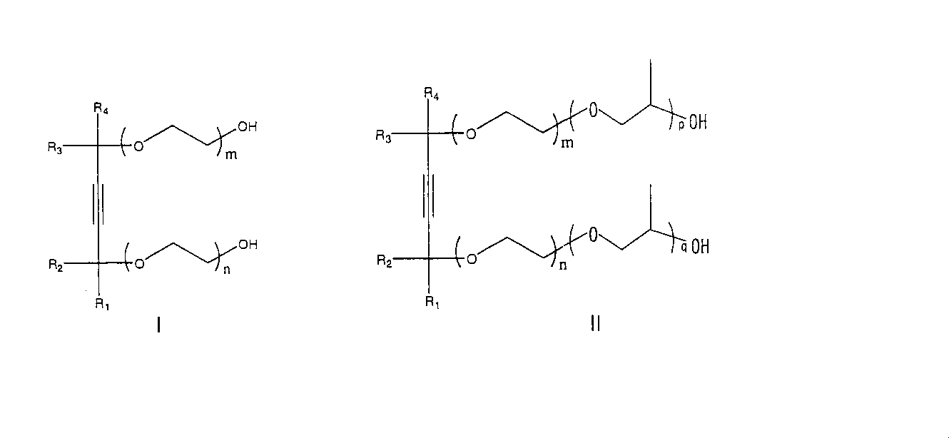
当該基材を次の式(I)又は(II)
を有する少なくとも1種の界面活性剤を約10ppm〜約10,000ppm含む処理溶液と接触させる工程、
を含む、半導体デバイス製造の際の欠陥低減方法。 A method for reducing defects in manufacturing a semiconductor device,
A step of preparing a substrate, and the substrate is represented by the following formula (I) or (II)
Contacting with a treatment solution comprising about 10 ppm to about 10,000 ppm of at least one surfactant having
A method for reducing defects in manufacturing a semiconductor device.
基材を用意する工程、及び
当該基材を下式
を有する少なくとも1種の界面活性剤を約10ppm〜約10,000ppm含む処理溶液と接触させる工程、
を含む、半導体デバイス製造の際の欠陥低減方法。 A method for reducing defects in manufacturing a semiconductor device,
A step of preparing a base material, and the base material
Contacting with a treatment solution comprising about 10 ppm to about 10,000 ppm of at least one surfactant having
A method for reducing defects in manufacturing a semiconductor device.
を有する少なくとも1種の界面活性剤を約10〜約10,000ppm含む処理溶液。 The following formula (I) or (II)
A treatment solution comprising from about 10 to about 10,000 ppm of at least one surfactant having the formula:
を有する少なくとも1種の界面活性剤を約10〜約10,000ppm含む処理溶液。 The following formula
A treatment solution comprising from about 10 to about 10,000 ppm of at least one surfactant having the formula:
Applications Claiming Priority (3)
| Application Number | Priority Date | Filing Date | Title |
|---|---|---|---|
| US10/218,087 US20040029395A1 (en) | 2002-08-12 | 2002-08-12 | Process solutions containing acetylenic diol surfactants |
| US10/339,709 US20040029396A1 (en) | 2002-08-12 | 2003-01-09 | Process solutions containing surfactants |
| US10/616,662 US7129199B2 (en) | 2002-08-12 | 2003-07-10 | Process solutions containing surfactants |
Related Parent Applications (1)
| Application Number | Title | Priority Date | Filing Date |
|---|---|---|---|
| JP2003292481A Division JP4272013B2 (en) | 2002-08-12 | 2003-08-12 | Defect reduction method and processing solution in semiconductor device manufacturing |
Related Child Applications (1)
| Application Number | Title | Priority Date | Filing Date |
|---|---|---|---|
| JP2009122006A Division JP4843068B2 (en) | 2002-08-12 | 2009-05-20 | Method for reducing the number of pattern collapse defects during semiconductor device manufacturing |
Publications (3)
| Publication Number | Publication Date |
|---|---|
| JP2006201809A JP2006201809A (en) | 2006-08-03 |
| JP2006201809A5 true JP2006201809A5 (en) | 2006-09-28 |
| JP4354964B2 JP4354964B2 (en) | 2009-10-28 |
Family
ID=30773450
Family Applications (2)
| Application Number | Title | Priority Date | Filing Date |
|---|---|---|---|
| JP2003292481A Expired - Fee Related JP4272013B2 (en) | 2002-08-12 | 2003-08-12 | Defect reduction method and processing solution in semiconductor device manufacturing |
| JP2006103543A Expired - Fee Related JP4354964B2 (en) | 2002-08-12 | 2006-04-04 | Development pattern collapse avoidance method and defect reduction method in semiconductor device manufacturing |
Family Applications Before (1)
| Application Number | Title | Priority Date | Filing Date |
|---|---|---|---|
| JP2003292481A Expired - Fee Related JP4272013B2 (en) | 2002-08-12 | 2003-08-12 | Defect reduction method and processing solution in semiconductor device manufacturing |
Country Status (5)
| Country | Link |
|---|---|
| US (4) | US7129199B2 (en) |
| EP (1) | EP1389746A3 (en) |
| JP (2) | JP4272013B2 (en) |
| KR (1) | KR20040030253A (en) |
| TW (1) | TWI247799B (en) |
Families Citing this family (91)
| Publication number | Priority date | Publication date | Assignee | Title |
|---|---|---|---|---|
| US7208049B2 (en) * | 2003-10-20 | 2007-04-24 | Air Products And Chemicals, Inc. | Process solutions containing surfactants used as post-chemical mechanical planarization treatment |
| US7348300B2 (en) * | 1999-05-04 | 2008-03-25 | Air Products And Chemicals, Inc. | Acetylenic diol ethylene oxide/propylene oxide adducts and processes for their manufacture |
| US7129199B2 (en) | 2002-08-12 | 2006-10-31 | Air Products And Chemicals, Inc. | Process solutions containing surfactants |
| US7521405B2 (en) * | 2002-08-12 | 2009-04-21 | Air Products And Chemicals, Inc. | Process solutions containing surfactants |
| US20040029395A1 (en) * | 2002-08-12 | 2004-02-12 | Peng Zhang | Process solutions containing acetylenic diol surfactants |
| US7459005B2 (en) * | 2002-11-22 | 2008-12-02 | Akzo Nobel N.V. | Chemical composition and method |
| JP4045180B2 (en) * | 2002-12-03 | 2008-02-13 | Azエレクトロニックマテリアルズ株式会社 | Rinsing liquid for lithography and resist pattern forming method using the same |
| JP4426526B2 (en) | 2003-07-17 | 2010-03-03 | ハネウエル・インターナシヨナル・インコーポレーテツド | State-of-the-art planarization films for microelectronics applications and devices and methods for their manufacture |
| US7446051B2 (en) * | 2003-09-09 | 2008-11-04 | Csg Solar Ag | Method of etching silicon |
| JP2007505486A (en) * | 2003-09-09 | 2007-03-08 | シーエスジー ソーラー アクチェンゲゼルシャフト | Mask adjustment by reflow |
| EP1665346A4 (en) * | 2003-09-09 | 2006-11-15 | Csg Solar Ag | Improved method of forming openings in an organic resin material |
| CN101065837A (en) * | 2004-03-30 | 2007-10-31 | 巴斯福股份公司 | Aqueous solution for removing post-etch residue |
| DE102004017440A1 (en) * | 2004-04-08 | 2005-11-03 | Enthone Inc., West Haven | Process for the treatment of laser-structured plastic surfaces |
| EP1598704B1 (en) | 2004-05-17 | 2009-12-02 | FUJIFILM Corporation | Pattern forming method |
| JP4759311B2 (en) * | 2004-05-17 | 2011-08-31 | 富士フイルム株式会社 | Pattern formation method |
| KR20070034519A (en) * | 2004-05-27 | 2007-03-28 | 이 아이 듀폰 디 네모아 앤드 캄파니 | Developer for photosensitive polymer protective layer |
| US7312152B2 (en) * | 2004-06-28 | 2007-12-25 | Intel Corporation | Lactate-containing corrosion inhibitor |
| US7611825B2 (en) * | 2004-09-15 | 2009-11-03 | Taiwan Semiconductor Manufacturing Company, Ltd. | Photolithography method to prevent photoresist pattern collapse |
| US7232759B2 (en) * | 2004-10-04 | 2007-06-19 | Applied Materials, Inc. | Ammonium hydroxide treatments for semiconductor substrates |
| US20060255315A1 (en) * | 2004-11-19 | 2006-11-16 | Yellowaga Deborah L | Selective removal chemistries for semiconductor applications, methods of production and uses thereof |
| JP2008521246A (en) * | 2004-11-19 | 2008-06-19 | ハネウエル・インターナシヨナル・インコーポレーテツド | Selective removal chemicals for semiconductor applications, methods for their production and their use |
| US7732123B2 (en) * | 2004-11-23 | 2010-06-08 | Taiwan Semiconductor Manufacturing Company, Ltd. | Immersion photolithography with megasonic rinse |
| US20060115774A1 (en) * | 2004-11-30 | 2006-06-01 | Taiwan Semiconductor Manufacturing Co., Ltd. | Method for reducing wafer charging during drying |
| KR100663354B1 (en) * | 2005-01-25 | 2007-01-02 | 삼성전자주식회사 | Methods of fabricating semiconductor device having photoresist removing process using photoresist stripping composition |
| JP4237184B2 (en) * | 2005-03-31 | 2009-03-11 | エルピーダメモリ株式会社 | Manufacturing method of semiconductor device |
| US20070087951A1 (en) * | 2005-10-19 | 2007-04-19 | Hynix Semiconductor Inc. | Thinner composition for inhibiting photoresist from drying |
| JP2007219009A (en) * | 2006-02-14 | 2007-08-30 | Az Electronic Materials Kk | Processing solvent for resist substrate and method for processing resist substrate using the same |
| JP4531726B2 (en) * | 2006-06-22 | 2010-08-25 | Azエレクトロニックマテリアルズ株式会社 | Method for forming miniaturized resist pattern |
| JP4866165B2 (en) * | 2006-07-10 | 2012-02-01 | 大日本スクリーン製造株式会社 | Substrate development processing method and substrate development processing apparatus |
| JP2008102343A (en) | 2006-10-19 | 2008-05-01 | Az Electronic Materials Kk | Developed resist substrate processing liquid and method of processing resist substrate using the same |
| JP5000260B2 (en) * | 2006-10-19 | 2012-08-15 | AzエレクトロニックマテリアルズIp株式会社 | Method for forming fine pattern and resist substrate processing liquid used therefor |
| US8530148B2 (en) * | 2006-12-25 | 2013-09-10 | Fujifilm Corporation | Pattern forming method, resist composition for multiple development used in the pattern forming method, developer for negative development used in the pattern forming method, and rinsing solution for negative development used in the pattern forming method |
| JP4554665B2 (en) | 2006-12-25 | 2010-09-29 | 富士フイルム株式会社 | PATTERN FORMATION METHOD, POSITIVE RESIST COMPOSITION FOR MULTIPLE DEVELOPMENT USED FOR THE PATTERN FORMATION METHOD, NEGATIVE DEVELOPMENT SOLUTION USED FOR THE PATTERN FORMATION METHOD, AND NEGATIVE DEVELOPMENT RINSE SOLUTION USED FOR THE PATTERN FORMATION METHOD |
| US8637229B2 (en) * | 2006-12-25 | 2014-01-28 | Fujifilm Corporation | Pattern forming method, resist composition for multiple development used in the pattern forming method, developer for negative development used in the pattern forming method, and rinsing solution for negative development used in the pattern forming method |
| US8034547B2 (en) * | 2007-04-13 | 2011-10-11 | Fujifilm Corporation | Pattern forming method, resist composition to be used in the pattern forming method, negative developing solution to be used in the pattern forming method and rinsing solution for negative development to be used in the pattern forming method |
| US8603733B2 (en) | 2007-04-13 | 2013-12-10 | Fujifilm Corporation | Pattern forming method, and resist composition, developer and rinsing solution used in the pattern forming method |
| WO2008129964A1 (en) | 2007-04-13 | 2008-10-30 | Fujifilm Corporation | Method for pattern formation, and resist composition, developing solution and rinsing liquid for use in the method for pattern formation |
| US8476001B2 (en) | 2007-05-15 | 2013-07-02 | Fujifilm Corporation | Pattern forming method |
| US7985534B2 (en) * | 2007-05-15 | 2011-07-26 | Fujifilm Corporation | Pattern forming method |
| US8617794B2 (en) | 2007-06-12 | 2013-12-31 | Fujifilm Corporation | Method of forming patterns |
| JP4617337B2 (en) * | 2007-06-12 | 2011-01-26 | 富士フイルム株式会社 | Pattern formation method |
| US8632942B2 (en) | 2007-06-12 | 2014-01-21 | Fujifilm Corporation | Method of forming patterns |
| JP4590431B2 (en) * | 2007-06-12 | 2010-12-01 | 富士フイルム株式会社 | Pattern formation method |
| KR101452229B1 (en) * | 2007-06-12 | 2014-10-22 | 후지필름 가부시키가이샤 | Resist composition for negative tone development and pattern forming method using the same |
| US20090253268A1 (en) * | 2008-04-03 | 2009-10-08 | Honeywell International, Inc. | Post-contact opening etchants for post-contact etch cleans and methods for fabricating the same |
| CN201219685Y (en) * | 2008-04-16 | 2009-04-15 | 韩广民 | Assembling structure product and yard chair |
| JP5306755B2 (en) * | 2008-09-16 | 2013-10-02 | AzエレクトロニックマテリアルズIp株式会社 | Substrate processing liquid and resist substrate processing method using the same |
| BRPI0920545A2 (en) | 2008-10-09 | 2015-12-29 | Avantor Performance Mat Inc | aqueous acidic formulations for removal of corrosive copper oxide residues and prevention of copper electroplating |
| JP2010128464A (en) | 2008-12-01 | 2010-06-10 | Az Electronic Materials Kk | Method for forming resist pattern |
| US8216384B2 (en) * | 2009-01-15 | 2012-07-10 | Intermolecular, Inc. | Combinatorial approach to the development of cleaning formulations for wet removal of high dose implant photoresist |
| JP2012516380A (en) | 2009-01-28 | 2012-07-19 | アドバンスド テクノロジー マテリアルズ,インコーポレイテッド | In situ cleaning formulation for lithographic tools |
| US8309502B2 (en) | 2009-03-27 | 2012-11-13 | Eastman Chemical Company | Compositions and methods for removing organic substances |
| US8444768B2 (en) | 2009-03-27 | 2013-05-21 | Eastman Chemical Company | Compositions and methods for removing organic substances |
| US8614053B2 (en) * | 2009-03-27 | 2013-12-24 | Eastman Chemical Company | Processess and compositions for removing substances from substrates |
| JP5448536B2 (en) | 2009-04-08 | 2014-03-19 | 東京エレクトロン株式会社 | Resist coating and developing apparatus, resist coating and developing method, resist film processing apparatus and resist film processing method |
| JP5193121B2 (en) * | 2009-04-17 | 2013-05-08 | 東京エレクトロン株式会社 | Resist coating and development method |
| JP5159738B2 (en) * | 2009-09-24 | 2013-03-13 | 株式会社東芝 | Semiconductor substrate cleaning method and semiconductor substrate cleaning apparatus |
| US20110253171A1 (en) * | 2010-04-15 | 2011-10-20 | John Moore | Chemical Composition and Methods for Removing Epoxy-Based Photoimageable Coatings Utilized In Microelectronic Fabrication |
| JP5591623B2 (en) * | 2010-08-13 | 2014-09-17 | AzエレクトロニックマテリアルズIp株式会社 | Rinsing liquid for lithography and pattern forming method using the same |
| JP5771035B2 (en) * | 2011-03-29 | 2015-08-26 | 株式会社Screenホールディングス | Substrate processing method and substrate processing apparatus |
| KR101266620B1 (en) | 2010-08-20 | 2013-05-22 | 다이닛뽕스크린 세이조오 가부시키가이샤 | Substrate processing method and substrate processing apparatus |
| JP5657318B2 (en) * | 2010-09-27 | 2015-01-21 | 富士フイルム株式会社 | Semiconductor substrate cleaning agent, cleaning method using the same, and semiconductor device manufacturing method |
| JP5659873B2 (en) | 2010-12-16 | 2015-01-28 | 富士通株式会社 | Resist pattern improving material, resist pattern forming method, and semiconductor device manufacturing method |
| RU2584204C2 (en) * | 2011-01-25 | 2016-05-20 | Басф Се | Use of surfactants, containing at least three short-chain perfluorinated groups, for production of microchips, having patterns with distance between lines of less than 50 nm |
| JP5708071B2 (en) | 2011-03-11 | 2015-04-30 | 富士通株式会社 | Resist pattern improving material, resist pattern forming method, and semiconductor device manufacturing method |
| US9275851B2 (en) * | 2011-03-21 | 2016-03-01 | Basf Se | Aqueous, nitrogen-free cleaning composition and its use for removing residues and contaminants from semiconductor substrates suitable for manufacturing microelectronic devices |
| JP5705607B2 (en) * | 2011-03-23 | 2015-04-22 | メルクパフォーマンスマテリアルズIp合同会社 | Rinsing liquid for lithography and pattern forming method using the same |
| US20130040246A1 (en) * | 2011-08-09 | 2013-02-14 | Tokyo Electron Limited | Multiple chemical treatment process for reducing pattern defect |
| US8987181B2 (en) * | 2011-11-08 | 2015-03-24 | Dynaloy, Llc | Photoresist and post etch residue cleaning solution |
| US9097977B2 (en) | 2012-05-15 | 2015-08-04 | Tokyo Electron Limited | Process sequence for reducing pattern roughness and deformity |
| RU2015104112A (en) | 2012-07-10 | 2016-08-27 | Басф Се | COMPOSITIONS FOR PROCESSING PREVENTING COLLAPSE OF THE DRAWING OF ELEMENTS OF THE SCHEME INCLUDING DIMERIC ADDITIVES |
| KR101993360B1 (en) | 2012-08-08 | 2019-06-26 | 삼성전자주식회사 | Phto lithographic rinse solution |
| JP6106990B2 (en) * | 2012-08-27 | 2017-04-05 | 富士通株式会社 | Lithographic rinse agent, resist pattern forming method, and semiconductor device manufacturing method |
| JP6012377B2 (en) | 2012-09-28 | 2016-10-25 | 東京応化工業株式会社 | Resist pattern forming method |
| US9029268B2 (en) | 2012-11-21 | 2015-05-12 | Dynaloy, Llc | Process for etching metals |
| US9660745B2 (en) * | 2012-12-12 | 2017-05-23 | At&T Intellectual Property I, L.P. | Geocast-based file transfer |
| SG11201504607QA (en) * | 2012-12-14 | 2015-07-30 | Basf Se | Use of compositions comprising a surfactant and a hydrophobizer for avoiding anti pattern collapse when treating patterned materials with line-space dimensions of 50 nm or below |
| US10170297B2 (en) * | 2013-08-22 | 2019-01-01 | Versum Materials Us, Llc | Compositions and methods using same for flowable oxide deposition |
| KR20150051478A (en) | 2013-11-04 | 2015-05-13 | 삼성디스플레이 주식회사 | Photoresist composition and method of fabricating thin film transistor substrate using the same |
| US10073351B2 (en) | 2014-12-23 | 2018-09-11 | Versum Materials Us, Llc | Semi-aqueous photoresist or semiconductor manufacturing residue stripping and cleaning composition with improved silicon passivation |
| US9873833B2 (en) | 2014-12-29 | 2018-01-23 | Versum Materials Us, Llc | Etchant solutions and method of use thereof |
| US9482957B1 (en) * | 2015-06-15 | 2016-11-01 | I-Shan Ke | Solvent for reducing resist consumption and method using solvent for reducing resist consumption |
| US9652841B2 (en) * | 2015-07-06 | 2017-05-16 | International Business Machines Corporation | System and method for characterizing NANO/MICRO bubbles for particle recovery |
| CN106559086B (en) * | 2015-09-30 | 2019-02-15 | 努比亚技术有限公司 | Mobile terminal and wireless communications method |
| KR102507301B1 (en) | 2015-12-23 | 2023-03-07 | 삼성전자주식회사 | Photolithographic rinse solution and method of manufacturing integrated circuit device using the same |
| KR102152665B1 (en) * | 2016-03-31 | 2020-09-07 | 후지필름 가부시키가이샤 | Processing liquid for semiconductor manufacturing, and pattern formation method |
| WO2018095885A1 (en) * | 2016-11-25 | 2018-05-31 | Az Electronic Materials (Luxembourg) S.A.R.L. | A lithography composition, a method for forming resist patterns and a method for making semiconductor devices |
| KR102373044B1 (en) | 2017-02-20 | 2022-03-11 | 후지필름 가부시키가이샤 | Drug solution, drug solution receptor, and pattern formation method |
| JP2019121795A (en) * | 2017-12-27 | 2019-07-22 | 花王株式会社 | Manufacturing method of silicon wafer |
| US20190374982A1 (en) * | 2018-06-06 | 2019-12-12 | Tokyo Ohka Kogyo Co., Ltd. | Method for treating substrate and rinsing liquid |
| KR102475952B1 (en) * | 2018-06-22 | 2022-12-09 | 메르크 파텐트 게엠베하 | Photoresist compositions and methods of making photoresist coatings, etched photoresist coatings and etched Si containing layer(s), and methods of making devices using them |
Family Cites Families (61)
| Publication number | Priority date | Publication date | Assignee | Title |
|---|---|---|---|---|
| US55660A (en) * | 1866-06-19 | Improvement in gang-plows | ||
| US115022A (en) * | 1871-05-23 | Improvement in pulley-blocks | ||
| US4711917A (en) * | 1985-02-07 | 1987-12-08 | Ppg Industries, Inc. | Cationic coating compositions for electrodeposition over rough steel |
| JPS6232453A (en) * | 1985-08-06 | 1987-02-12 | Tokyo Ohka Kogyo Co Ltd | Developing solution for positive type photoresist |
| AU6629286A (en) | 1985-11-27 | 1987-07-01 | Macdermid, Inc. | Thermally stabilized photoresist images |
| US4824763A (en) * | 1987-07-30 | 1989-04-25 | Ekc Technology, Inc. | Triamine positive photoresist stripping composition and prebaking process |
| JPS6488547A (en) | 1987-09-30 | 1989-04-03 | Toshiba Corp | Production of semiconductor device |
| JP2670711B2 (en) * | 1990-05-29 | 1997-10-29 | 富士写真フイルム株式会社 | Developer for negative photosensitive resin composition |
| US5279771A (en) * | 1990-11-05 | 1994-01-18 | Ekc Technology, Inc. | Stripping compositions comprising hydroxylamine and alkanolamine |
| US6110881A (en) * | 1990-11-05 | 2000-08-29 | Ekc Technology, Inc. | Cleaning solutions including nucleophilic amine compound having reduction and oxidation potentials |
| US5127571A (en) * | 1991-10-31 | 1992-07-07 | International Business Machines Corporation | Water soluble soldering preflux and method of application |
| JPH07142349A (en) | 1993-11-16 | 1995-06-02 | Mitsubishi Electric Corp | Method for preventing tilting of photoresist pattern in developing step |
| CA2136373A1 (en) * | 1993-11-29 | 1995-05-30 | Steven W. Medina | Ethoxylated acetylenic glycols having low dynamic surface tension |
| US5474877A (en) | 1994-02-24 | 1995-12-12 | Nec Corporation | Method for developing a resist pattern |
| US5466389A (en) * | 1994-04-20 | 1995-11-14 | J. T. Baker Inc. | PH adjusted nonionic surfactant-containing alkaline cleaner composition for cleaning microelectronics substrates |
| JPH088163A (en) | 1994-06-21 | 1996-01-12 | Sony Corp | Pattern formation method |
| JP3121743B2 (en) | 1994-08-10 | 2001-01-09 | 日立造船株式会社 | Plasma melting method |
| JPH098163A (en) | 1995-06-22 | 1997-01-10 | Nippon Avionics Co Ltd | Semiconductor hermetically sealed package |
| JP2911792B2 (en) * | 1995-09-29 | 1999-06-23 | 東京応化工業株式会社 | Stripper composition for resist |
| US5948464A (en) * | 1996-06-19 | 1999-09-07 | Imra America, Inc. | Process of manufacturing porous separator for electrochemical power supply |
| US6030932A (en) | 1996-09-06 | 2000-02-29 | Olin Microelectronic Chemicals | Cleaning composition and method for removing residues |
| JPH10171128A (en) | 1996-12-10 | 1998-06-26 | Tokuyama Corp | Thick aqueous solution of tetramethylammonium hydroxide |
| US5977041A (en) * | 1997-09-23 | 1999-11-02 | Olin Microelectronic Chemicals | Aqueous rinsing composition |
| US6261466B1 (en) * | 1997-12-11 | 2001-07-17 | Shipley Company, L.L.C. | Composition for circuit board manufacture |
| WO1999060448A1 (en) | 1998-05-18 | 1999-11-25 | Mallinckrodt Inc. | Silicate-containing alkaline compositions for cleaning microelectronic substrates |
| JP3606738B2 (en) * | 1998-06-05 | 2005-01-05 | 東京応化工業株式会社 | Treatment liquid after ashing and treatment method using the same |
| US6368421B1 (en) | 1998-07-10 | 2002-04-09 | Clariant Finance (Bvi) Limited | Composition for stripping photoresist and organic materials from substrate surfaces |
| US6152148A (en) * | 1998-09-03 | 2000-11-28 | Honeywell, Inc. | Method for cleaning semiconductor wafers containing dielectric films |
| US7129199B2 (en) | 2002-08-12 | 2006-10-31 | Air Products And Chemicals, Inc. | Process solutions containing surfactants |
| US20040029395A1 (en) | 2002-08-12 | 2004-02-12 | Peng Zhang | Process solutions containing acetylenic diol surfactants |
| US6864395B2 (en) | 1999-05-04 | 2005-03-08 | Air Products And Chemicals, Inc. | Acetylenic diol ethylene oxide/propylene oxide adducts and processes for their manufacture |
| US7521405B2 (en) * | 2002-08-12 | 2009-04-21 | Air Products And Chemicals, Inc. | Process solutions containing surfactants |
| US6313182B1 (en) * | 1999-05-04 | 2001-11-06 | Air Products And Chemicals, Inc. | Acetylenic diol ethylene oxide/propylene oxide adducts and processes for their manufacture |
| US7348300B2 (en) * | 1999-05-04 | 2008-03-25 | Air Products And Chemicals, Inc. | Acetylenic diol ethylene oxide/propylene oxide adducts and processes for their manufacture |
| US6455234B1 (en) * | 1999-05-04 | 2002-09-24 | Air Products And Chemicals, Inc. | Acetylenic diol ethylene oxide/propylene oxide adducts and their use in photoresist developers |
| JP2001033988A (en) | 1999-07-15 | 2001-02-09 | Tokyo Ohka Kogyo Co Ltd | Rinsing solution for photolithography, and treatment of substrate using same |
| US6251745B1 (en) * | 1999-08-18 | 2001-06-26 | Taiwan Semiconductor Manufacturing Company | Two-dimensional scaling method for determining the overlay error and overlay process window for integrated circuits |
| US6369146B1 (en) * | 1999-10-26 | 2002-04-09 | Air Products And Chemicals, Inc. | Malic acid diester surfactants |
| JP2001215690A (en) | 2000-01-04 | 2001-08-10 | Air Prod And Chem Inc | Acetylenic diol ethylene oxide/propylene oxide adducts and their use in photoresis developer |
| US6268115B1 (en) * | 2000-01-06 | 2001-07-31 | Air Products And Chemicals, Inc. | Use of alkylated polyamines in photoresist developers |
| TW558736B (en) | 2000-02-26 | 2003-10-21 | Shipley Co Llc | Method of reducing defects |
| US6310019B1 (en) * | 2000-07-05 | 2001-10-30 | Wako Pure Chemical Industries, Ltd. | Cleaning agent for a semi-conductor substrate |
| WO2002023598A2 (en) | 2000-09-15 | 2002-03-21 | Infineon Technologies North America Corp. | A method to reduce post-development defects without sacrificing throughput |
| US6599370B2 (en) * | 2000-10-16 | 2003-07-29 | Mallinckrodt Inc. | Stabilized alkaline compositions for cleaning microelectronic substrates |
| US6451510B1 (en) | 2001-02-21 | 2002-09-17 | International Business Machines Corporation | Developer/rinse formulation to prevent image collapse in resist |
| US6413914B1 (en) | 2001-03-29 | 2002-07-02 | Air Products And Chemicals, Inc. | Low foam N,N′-dialkylmalamide wetting agents |
| JP2003010774A (en) | 2001-06-27 | 2003-01-14 | Nippon Paint Co Ltd | Method of coating metallic material |
| MY131912A (en) * | 2001-07-09 | 2007-09-28 | Avantor Performance Mat Inc | Ammonia-free alkaline microelectronic cleaning compositions with improved substrate compatibility |
| US6656977B2 (en) * | 2001-07-20 | 2003-12-02 | Air Products And Chemical, Inc. | Alkyl glycidyl ether-capped polyamine foam control agents |
| US6762208B2 (en) * | 2001-10-01 | 2004-07-13 | Air Products And Chemicals, Inc. | Alkane diol foam controlling agents |
| US6641986B1 (en) * | 2002-08-12 | 2003-11-04 | Air Products And Chemicals, Inc. | Acetylenic diol surfactant solutions and methods of using same |
| JP4045180B2 (en) | 2002-12-03 | 2008-02-13 | Azエレクトロニックマテリアルズ株式会社 | Rinsing liquid for lithography and resist pattern forming method using the same |
| JP4085262B2 (en) * | 2003-01-09 | 2008-05-14 | 三菱瓦斯化学株式会社 | Resist stripper |
| US6951710B2 (en) * | 2003-05-23 | 2005-10-04 | Air Products And Chemicals, Inc. | Compositions suitable for removing photoresist, photoresist byproducts and etching residue, and use thereof |
| DE602004009595T2 (en) * | 2003-08-19 | 2008-07-24 | Mallinckrodt Baker, Inc. | REMOVAL AND CLEANING COMPOSITIONS FOR MICROELECTRONICS |
| TWI417683B (en) * | 2006-02-15 | 2013-12-01 | Avantor Performance Mat Inc | Stabilized, non-aqueous cleaning compositions for microelectronics substrates |
| US20080076688A1 (en) * | 2006-09-21 | 2008-03-27 | Barnes Jeffrey A | Copper passivating post-chemical mechanical polishing cleaning composition and method of use |
| US20100261632A1 (en) * | 2007-08-02 | 2010-10-14 | Advanced Technology Materials, Inc. | Non-fluoride containing composition for the removal of residue from a microelectronic device |
| US7976638B2 (en) * | 2007-11-13 | 2011-07-12 | Sachem, Inc. | High negative zeta potential polyhedral silsesquioxane composition and method for damage free semiconductor wet clean |
| US20100105595A1 (en) * | 2008-10-29 | 2010-04-29 | Wai Mun Lee | Composition comprising chelating agents containing amidoxime compounds |
| US8765653B2 (en) * | 2009-07-07 | 2014-07-01 | Air Products And Chemicals, Inc. | Formulations and method for post-CMP cleaning |
-
2003
- 2003-07-10 US US10/616,662 patent/US7129199B2/en not_active Expired - Lifetime
- 2003-08-06 TW TW092121575A patent/TWI247799B/en not_active IP Right Cessation
- 2003-08-07 EP EP03017570A patent/EP1389746A3/en not_active Withdrawn
- 2003-08-12 KR KR1020030055727A patent/KR20040030253A/en not_active Application Discontinuation
- 2003-08-12 JP JP2003292481A patent/JP4272013B2/en not_active Expired - Fee Related
-
2006
- 2006-04-04 JP JP2006103543A patent/JP4354964B2/en not_active Expired - Fee Related
- 2006-09-14 US US11/520,971 patent/US7591270B2/en not_active Expired - Lifetime
- 2006-09-14 US US11/520,983 patent/US20070010412A1/en not_active Abandoned
-
2010
- 2010-07-29 US US12/846,369 patent/US8227395B2/en not_active Expired - Lifetime
Similar Documents
| Publication | Publication Date | Title |
|---|---|---|
| JP2006201809A5 (en) | ||
| JP7171800B2 (en) | Cleaning formulations to remove residues on surfaces | |
| US11124704B2 (en) | Etching compositions | |
| KR102283723B1 (en) | Cleaning formulation for removing residues on surfaces | |
| JP2011515872A5 (en) | ||
| TW201610234A (en) | Etching solution composition and etching method | |
| KR102242951B1 (en) | Solution for etching silicon oxide layer | |
| CN108780747B (en) | Etching liquid composition and etching method | |
| CN114258424B (en) | Etching composition | |
| Stapf et al. | HF-(NH4) 2S2O8-HCl Mixtures for HNO3-and NO x-free Etching of Diamond Wire-and SiC-Slurry-Sawn Silicon Wafers: Reactivity Studies, Surface Chemistry, and Unexpected Pyramidal Surface Morphologies | |
| US11268024B2 (en) | Etching compositions | |
| JP2013104954A (en) | Wafer surface treatment method and surface treatment liquid | |
| TWI488960B (en) | Cleaning liquid for semiconductor device and cleaning method | |
| KR20150088356A (en) | Etching composition for silicon-based compound layer | |
| KR20090012953A (en) | Etching solution for semiconductor device and method of making the semiconductor device using the same | |
| TW202235683A (en) | Wet etching solution and wet etching method | |
| KR101478596B1 (en) | Silicone solvent | |
| US9914847B2 (en) | Resin composition for forming a phase-separated structure, and method of producing structure containing phase-separated structure | |
| TWI801608B (en) | Composition for surface treatment, film comprising the same, and method for surface treatment using the same | |
| TW201323595A (en) | Wafer surface-treatment method and surface-treatment liquid, and surface-treatment agent, surface-treatment liquid, and surface-treatment method for silicon-nitride-containing wafers | |
| WO2022080288A1 (en) | Wet etching method | |
| TW202346643A (en) | Etching compositions | |
| TW202336214A (en) | Etching compositions | |
| WO2023064145A1 (en) | Etching compositions | |
| TW202012703A (en) | Etching compositions |