JP2006201542A - Electrophotographic photoreceptor and image forming method using the same - Google Patents
Electrophotographic photoreceptor and image forming method using the same Download PDFInfo
- Publication number
- JP2006201542A JP2006201542A JP2005013742A JP2005013742A JP2006201542A JP 2006201542 A JP2006201542 A JP 2006201542A JP 2005013742 A JP2005013742 A JP 2005013742A JP 2005013742 A JP2005013742 A JP 2005013742A JP 2006201542 A JP2006201542 A JP 2006201542A
- Authority
- JP
- Japan
- Prior art keywords
- photosensitive member
- electrophotographic photosensitive
- layer
- image forming
- latent image
- Prior art date
- Legal status (The legal status is an assumption and is not a legal conclusion. Google has not performed a legal analysis and makes no representation as to the accuracy of the status listed.)
- Pending
Links
Images


Abstract
Description
本発明は、接触または近接して設けられた直流成分に交流成分を重畳した電圧を印加することによって生じる放電を利用して電子写真感光体を帯電させる帯電器を有する電子写真プロセスに採用した電子写真感光体、画像形成装置、画像形成装置用プロセスカートリッジ、画像形成法に関する。 The present invention relates to an electrophotographic process employed in an electrophotographic process having a charger that charges an electrophotographic photosensitive member by using a discharge generated by applying a voltage in which an alternating current component is superimposed on a direct current component that is provided in contact with or in close proximity. The present invention relates to a photographic photosensitive member, an image forming apparatus, a process cartridge for the image forming apparatus, and an image forming method.
近年、オフィスの省スペース化やビジネスオポチュニティの拡大などの観点から、電子写真装置に対して、ますます小型化と高画質化が望まれている。
電子写真装置の小型化を図るために、電子写真プロセスの改良が多く成されているが、帯電プロセスにおいては、近接放電による帯電方式が多く採用される傾向がある。これは、電子写真感光体表面に帯電部材を接触させたり、非接触で近傍に帯電部材を配置させたりすることで近接放電を発生させ、電子写真感光体表面の帯電を行う方式である。本方式を用いれば、大がかりな帯電装置を必要としないために、装置の小型化には非常に有効である。また最近の近接帯電方式は、電子写真感光体上の帯電の均一性をはかるために、直流電圧に交流電圧を重畳して印加する方式を採用していることが多くなっている。
In recent years, miniaturization and higher image quality have been demanded for electrophotographic apparatuses from the viewpoints of saving office space and expanding business opportunities.
Many attempts have been made to improve the electrophotographic process in order to reduce the size of the electrophotographic apparatus. However, in the charging process, a charging method using proximity discharge tends to be frequently employed. This is a system in which a charging member is brought into contact with the surface of the electrophotographic photosensitive member, or a charging member is disposed in the vicinity without contact to generate a proximity discharge to charge the surface of the electrophotographic photosensitive member. If this method is used, a large-scale charging device is not required, and thus it is very effective for downsizing the device. Also, recent proximity charging systems often employ a system in which an AC voltage is applied in a superimposed manner on a DC voltage in order to achieve uniform charging on the electrophotographic photosensitive member.
しかし直流電圧に交流電圧を重畳した近接放電による帯電方式は電子写真感光体表面近傍に放電が集中するため、電子写真感光体表面を劣化させ、電子写真感光体の膜厚減少が大きいことがわかった。近接放電による電子写真感光体表面の劣化は機械的摺擦とは違い、像担持体への当接部材がない場合においても発生する。このため、近接放電に対する耐久性を有する電子写真感光体もしくは電子写真感光体表面の保護技術の開発が強く望まれている。 However, the charging method using proximity discharge in which AC voltage is superimposed on DC voltage concentrates the discharge near the surface of the electrophotographic photosensitive member, so the surface of the electrophotographic photosensitive member is deteriorated and the thickness of the electrophotographic photosensitive member is greatly reduced. It was. Deterioration of the electrophotographic photosensitive member surface due to proximity discharge occurs even when there is no contact member to the image carrier, unlike mechanical rubbing. For this reason, development of an electrophotographic photosensitive member having durability against proximity discharge or a technology for protecting the surface of the electrophotographic photosensitive member is strongly desired.
以下に近接放電による電子写真感光体表面の劣化メカニズムについて説明する。
図1は、近接放電による電子写真感光体表面の劣化状態を調べるために、電子写真感光体表面に帯電部材のみを非接触状態で近接配置し、連続約150時間の帯電実験を行ったときの、電子写真感光体表面の膜厚の変化を測定した結果である。
The deterioration mechanism of the electrophotographic photoreceptor surface due to proximity discharge will be described below.
FIG. 1 shows a state in which only a charging member is placed close to the surface of the electrophotographic photosensitive member in a non-contact state in order to investigate the deterioration state of the surface of the electrophotographic photosensitive member due to the proximity discharge, and a charging experiment is performed for about 150 hours continuously. 3 is a result of measuring a change in film thickness on the surface of the electrophotographic photosensitive member.
実験に使用した電子写真感光体は電荷輸送層にポリカーボネートを用いた有機感光体であり、電子写真感光体に対して当接する部材を全て取り除き、直流電圧に交流電圧を重畳した交番電圧が印加された非接触帯電ローラを用いて帯電を行った。この結果、電子写真感光体表面の膜の削れ量が次第に多くなり、電子写真感光体の膜厚が次第に減少している事実がわかった。膜厚減少のメカニズムについては今のところ検討中で明らかになってはいないが、膜厚が減少した電子写真感光体を分析したところ、電子写真感光体を構成するポリカーボネートが分解されたと考えられるカルボン酸などが検出された。 The electrophotographic photosensitive member used in the experiment is an organic photosensitive member using polycarbonate for the charge transport layer, and all the members in contact with the electrophotographic photosensitive member are removed, and an alternating voltage in which an alternating voltage is superimposed on a direct current voltage is applied. Charging was performed using a non-contact charging roller. As a result, it was found that the amount of film scraping on the surface of the electrophotographic photosensitive member gradually increased and the film thickness of the electrophotographic photosensitive member gradually decreased. The mechanism of film thickness reduction has not been clarified at present. However, when an electrophotographic photosensitive member having a reduced film thickness is analyzed, the polycarbonate constituting the electrophotographic photosensitive member is considered to have been decomposed. Acid etc. were detected.
このような物質が検出されたことから、電子写真感光体の膜厚減少のメカニズムとしては、次のようなことが考えられる。
図2(a)(b)は、近接放電によって電子写真感光体1表面が劣化する場合の電子写真感光体表面の状態を、帯電ローラ2aを電子写真感光体表面から微小ギャップをもって対向させた状態を例にとって示した説明図である。
Since such a substance has been detected, the following may be considered as a mechanism for reducing the film thickness of the electrophotographic photosensitive member.
FIGS. 2A and 2B show the state of the surface of the electrophotographic photosensitive member when the surface of the electrophotographic photosensitive member 1 deteriorates due to proximity discharge, and shows the state where the
近接放電を行うと、電子写真感光体表面の放電領域では放電により発生した粒子(オゾン、電子、励起分子、イオン、プラズマなど)のエネルギーが電子写真感光体表面の電荷輸送層1aに照射される。このエネルギーが電子写真感光体表面を構成する分子の結合エネルギーに共鳴、吸収され、図2(a)に示すように、電荷輸送層1aは、樹脂分子鎖の切断による分子量低下、高分子鎖の絡み合い度の低下等の化学的劣化を生じる。このような近接放電による電子写真感光体の化学的劣化によって、電子写真感光体表面の電荷輸送層1aは次第にその膜厚を減少させてしまうと考えられる。 When proximity discharge is performed, the energy of particles (ozone, electrons, excited molecules, ions, plasma, etc.) generated by the discharge is irradiated to the charge transport layer 1a on the surface of the electrophotographic photoreceptor in the discharge region on the surface of the electrophotographic photoreceptor. . This energy resonates and is absorbed by the binding energy of the molecules constituting the surface of the electrophotographic photosensitive member, and as shown in FIG. 2 (a), the charge transport layer 1a has a lower molecular weight due to cleavage of the resin molecular chain, Chemical degradation such as a decrease in the degree of entanglement occurs. It is considered that the film thickness of the charge transport layer 1a on the surface of the electrophotographic photosensitive member gradually decreases due to the chemical deterioration of the electrophotographic photosensitive member due to such proximity discharge.
この問題は、ポリカーボネートを用いた感光体にだけ起こる問題ではなく、ポリアリレート(特許文献1参照)、ポリスチレン(特許文献2参照)、アクリル樹脂(特許文献3参照)、ウレタン樹脂(特許文献4参照)等を用いた感光体においても同様な膜厚減少が起こり、本問題の解決には至っていない。 This problem is not only a problem that occurs in a photoreceptor using polycarbonate, but polyarylate (see Patent Document 1), polystyrene (see Patent Document 2), acrylic resin (see Patent Document 3), and urethane resin (see Patent Document 4). ) Etc., the same film thickness reduction occurs, and this problem has not been solved.
本発明は、直流電圧に交流電圧を重畳した近接放電による帯電方式において、電子写真感光体表面の劣化が少なく、且つ機械的耐久性が非常に良好であり、長期的に安定した画像形成を行うことが出来る電子写真感光体、及び画像形成方法を提供することを目的とする。 The present invention is a charging method using proximity discharge in which an AC voltage is superimposed on a DC voltage, and the surface of the electrophotographic photosensitive member is hardly deteriorated, the mechanical durability is very good, and stable image formation is performed over a long period of time. An object of the present invention is to provide an electrophotographic photosensitive member and an image forming method.
本発明者らは鋭意検討を重ねた結果、下記(1)〜(8)記載の感光体とすることにより、前期目的が達成できることを発見して本発明を成すに至った。
(1)『少なくとも電子写真感光体と、電子写真感光体に対して接触または近接して設けられた直流成分に交流成分を重畳した電圧を印加することによって生じる放電を利用して電子写真感光体を帯電させる帯電器と、帯電器によって帯電させられた電子写真感光体表面に静電潜像を形成する潜像形成器と、潜像形成器によって形成された静電潜像の画像部にトナーを付着させる現像器とを有する画像形成装置において用いる電子写真感光体であって、導電性支持体上に少なくとも感光層を有し、感光体の表面に平均粒子径20nm以下のカーボンを主成分とするナノ微粒子を含有することを特徴とする電子写真感光体』、
(2)『前記カーボンが、ダイヤモンド構造を有することを特徴とする上記(1)記載の電子写真感光体』、
(3)『前記感光層の上に表面層を有することを特徴とする上記(1)又は(2)記載の電子写真感光体』、
(4)『前記表面層が、ポリカーボネート、ポリエステル、ポリエーテルの少なくともいずれか1つの重合体を含有することを特徴とする上記(3)記載の電子写真感光体』、
(5)『前記表面層が、電荷輸送材料を含有することを特徴とする上記(4)記載の電子写真感光体』、
(6)『前記表面層が、少なくとも電荷輸送性構造を有しない3官能以上のラジカル重合性モノマーと電荷輸送性構造を有するラジカル重合性化合物を硬化した架橋樹脂層であることを特徴とする上記(3)記載の電子写真感光体』、
(7)『前記表面層に用いられている電荷輸送性構造を有するラジカル重合性化合物が、1官能であることを特徴とする上記(6)記載の電子写真感光体』、
(8)『前記感光層が、電荷発生層、電荷輸送層を順に積層した構造を有することを特徴とする上記(1)〜(7)記載の電子写真感光体』、
As a result of intensive studies, the present inventors have found that the purpose of the previous term can be achieved by using the photoreceptors described in (1) to (8) below, and have achieved the present invention.
(1) “At least an electrophotographic photosensitive member and an electrophotographic photosensitive member using a discharge generated by applying a voltage in which an alternating current component is superimposed on a direct current component provided in contact with or close to the electrophotographic photosensitive member. A charger for charging the toner, a latent image forming device for forming an electrostatic latent image on the surface of the electrophotographic photosensitive member charged by the charger, and a toner on an image portion of the electrostatic latent image formed by the latent image forming device. An electrophotographic photosensitive member used in an image forming apparatus having a developing device for adhering a toner, the photosensitive member having at least a photosensitive layer on a conductive support, and carbon having an average particle diameter of 20 nm or less on a surface of the photosensitive member as a main component. Electrophotographic photosensitive member characterized by containing nano-particles that can be used ",
(2) "The electrophotographic photosensitive member according to (1) above, wherein the carbon has a diamond structure",
(3) “The electrophotographic photosensitive member according to (1) or (2) above, which has a surface layer on the photosensitive layer”,
(4) "The electrophotographic photosensitive member according to (3) above, wherein the surface layer contains at least one polymer of polycarbonate, polyester, and polyether",
(5) "The electrophotographic photosensitive member according to (4) above, wherein the surface layer contains a charge transport material",
(6) “The surface layer is a cross-linked resin layer obtained by curing at least a trifunctional or higher-functional radical polymerizable monomer having no charge transport structure and a radical polymerizable compound having a charge transport structure. (3) The electrophotographic photosensitive member described in the above,
(7) “The electrophotographic photosensitive member according to (6) above, wherein the radical polymerizable compound having a charge transporting structure used in the surface layer is monofunctional”;
(8) "The electrophotographic photosensitive member according to any one of (1) to (7) above, wherein the photosensitive layer has a structure in which a charge generation layer and a charge transport layer are sequentially laminated",
また、本発明者らは鋭意検討を重ねた結果、下記(9)記載の画像形成装置とすることにより、前期目的が達成できることを発見して本発明を成すに至った。
(9)『少なくとも電子写真感光体と、電子写真感光体に対して接触または近接して設けられた直流成分に交流成分を重畳した電圧を印加することによって生じる放電を利用して電子写真感光体を帯電させる帯電器と、帯電器によって帯電させられた電子写真感光体表面に静電潜像を形成する潜像形成器と、潜像形成器によって形成された静電潜像の画像部にトナーを付着させる現像器とを有する画像形成装置において、該電子写真感光体が上記(1)〜(8)記載の電子写真感光体であることを特徴とする画像形成装置』、
In addition, as a result of intensive studies, the present inventors have found that the purpose of the previous period can be achieved by using the image forming apparatus described in (9) below, and have achieved the present invention.
(9) “An electrophotographic photosensitive member utilizing at least an electrophotographic photosensitive member and a discharge generated by applying a voltage in which an alternating current component is superimposed on a direct current component provided in contact with or close to the electrophotographic photosensitive member. A charger for charging the toner, a latent image forming device for forming an electrostatic latent image on the surface of the electrophotographic photosensitive member charged by the charger, and a toner on an image portion of the electrostatic latent image formed by the latent image forming device. An image forming apparatus having a developing device for adhering the electrophotographic photosensitive member, wherein the electrophotographic photosensitive member is the electrophotographic photosensitive member according to (1) to (8) above, ”
更に、前記課題は、下記(10)記載のプロセスカートリッジ及び下記(11)記載の画像形成方法により解決される。
(10)『上記(1)〜(8)記載の電子写真感光体を有することを特徴とするプロセスカートリッジ。
(11)『上記(9に記載の画像形成装置を用いて画像を形成することを特徴とする画像形成方法。
Further, the above problem is solved by a process cartridge described in (10) below and an image forming method described in (11) below.
(10) “A process cartridge comprising the electrophotographic photosensitive member according to the above (1) to (8).
(11) “An image forming method, wherein an image is formed using the image forming apparatus described in (9).
少なくとも電子写真感光体と、電子写真感光体に対して接触または近接して設けられた直流成分に交流成分を重畳した電圧を印加することによって生じる放電を利用して電子写真感光体を帯電させる帯電器と、帯電器によって帯電させられた電子写真感光体表面に静電潜像を形成する潜像形成器と、潜像形成器によって形成された静電潜像の画像部にトナーを付着させる現像器を有する画像形成装置において、該電子写真感光体が導電性支持体上に少なくとも感光層に有し、該感光体の表面に平均粒子径20nm以下のカーボンを主成分とするナノ微粒子を含有していることを特徴とする電子写真感光体とすることにより、帯電による電子写真感光体の劣化が少なく、且つ耐摩耗性が高く、良好な電気特性を有する、高耐久、高性能な電子写真感光体が得られる。
したがって、この電子写真感光体を用いることにより良好な画像を長期にわたり提供できる高性能で且つ信頼性の高い画像形成プロセス、画像形成装置及び画像形成装置用プロセスカートリッジが提供できる。
Charging that charges the electrophotographic photosensitive member using at least an electrophotographic photosensitive member and a discharge generated by applying a voltage in which the alternating current component is superimposed on a direct current component that is in contact with or close to the electrophotographic photosensitive member. , A latent image forming device for forming an electrostatic latent image on the surface of the electrophotographic photosensitive member charged by the charging device, and development for attaching toner to an image portion of the electrostatic latent image formed by the latent image forming device. In the image forming apparatus having a container, the electrophotographic photosensitive member has at least a photosensitive layer on a conductive support, and the surface of the photosensitive member contains nanoparticles having an average particle diameter of 20 nm or less as a main component. The electrophotographic photosensitive member is characterized in that the electrophotographic photosensitive member is less deteriorated due to charging, has high wear resistance, has good electrical characteristics, and has high durability and high performance. Photoreceptor is obtained.
Therefore, by using this electrophotographic photosensitive member, it is possible to provide a high-performance and highly reliable image forming process, an image forming apparatus, and a process cartridge for the image forming apparatus that can provide good images over a long period of time.
以下、本発明について詳細に説明する。
本発明は、少なくとも電子写真感光体と、電子写真感光体に対して接触または近接して設けられた直流成分に交流成分を重畳した電圧を印加することによって生じる放電を利用して電子写真感光体を帯電させる帯電器と、帯電器によって帯電させられた電子写真感光体表面に静電潜像を形成する潜像形成器と、潜像形成器によって形成された静電潜像の画像部にトナーを付着させる現像器を有する画像形成装置において、該電子写真感光体が導電性支持体上に少なくとも感光層に有し、該感光体の表面に平均粒子径20nm以下のカーボンを主成分とするナノ微粒子を含有していることを特徴とする電子写真感光体により達成されるものである。
Hereinafter, the present invention will be described in detail.
The present invention relates to an electrophotographic photosensitive member using at least an electrophotographic photosensitive member and a discharge generated by applying a voltage in which an alternating current component is superimposed on a direct current component provided in contact with or close to the electrophotographic photosensitive member. A charger for charging the toner, a latent image forming device for forming an electrostatic latent image on the surface of the electrophotographic photosensitive member charged by the charger, and a toner on an image portion of the electrostatic latent image formed by the latent image forming device. In the image forming apparatus having a developing unit for adhering the toner, the electrophotographic photosensitive member has at least a photosensitive layer on a conductive support, and a nano particle mainly composed of carbon having an average particle diameter of 20 nm or less on the surface of the photosensitive member. This is achieved by an electrophotographic photosensitive member characterized by containing fine particles.
本発明者が鋭意検討した結果、直流電圧に交流電圧を重畳した近接放電による帯電方式を用いた帯電器を用いた場合、機械的耐久性だけではなく、放電により発生した粒子(オゾン、電子、励起分子、イオン、プラズマなど)のエネルギー照射に対しても、非常に高い耐久性を有していることが判明した。 As a result of intensive studies by the inventor, when a charger using a charging method based on proximity discharge in which an AC voltage is superimposed on a DC voltage is used, not only mechanical durability but also particles (ozone, electrons, It has been found that it has extremely high durability against energy irradiation of excited molecules, ions, plasma, and the like.
大西ら(J. Electrochem. Soc., 130, 1, 143−146 (1983))によると、ドライエッチングプロセスにおいて、レジスト膜構造中の炭素数とエッチング速度は相関しており、炭素数が多くなるほど、エッチング速度が低下することが知られている。 According to Onishi et al. (J. Electrochem. Soc., 130, 1, 143-146 (1983)), in the dry etching process, the number of carbons in the resist film structure correlates with the etching rate, and as the number of carbons increases. It is known that the etching rate decreases.
直流電圧に交流電圧を重畳した近接放電による帯電方式においても、放電領域では、大気下でのプラズマ状態が発生しているものと考えられ、カーボンを主成分とするナノ微粒子を含有することにより、膜中のカーボン量が増加することから、耐久性が向上しているものと考えられる。 Even in the charging method using proximity discharge in which an alternating voltage is superimposed on a direct current voltage, it is considered that a plasma state is generated in the discharge region in the discharge region, and by containing nano-particles mainly composed of carbon, Since the amount of carbon in the film increases, it is considered that the durability is improved.
カーボンを主成分とするナノ微粒子は、粒径が大きい場合、感光体の表面粗さが大きくなる。表面粗さが大きい感光体では、感光体表面上にトナーを現像した場合、トナーが散りやすく、画像上で、トナー散り、地汚れ発生の原因となる。またクリーニング性も低下し、異常画像の原因となる。
本発明者らが検討した結果、カーボンを主成分とするナノ微粒子の平均粒径が、20nm以下である時に、感光体の表面は良好となる。
When the nanoparticle mainly composed of carbon has a large particle size, the surface roughness of the photoreceptor increases. In the case of a photoreceptor having a large surface roughness, when toner is developed on the surface of the photoreceptor, the toner is likely to be scattered, which causes the toner to be scattered on the image and to cause background contamination. In addition, the cleaning property is lowered, which causes an abnormal image.
As a result of investigations by the present inventors, the surface of the photoreceptor is good when the average particle size of the nano-particles mainly composed of carbon is 20 nm or less.
またカーボンを主成分とするナノ微粒子は、平均粒径が50nm以下好ましくは20nm以下の場合、長期的使用時に、膜表面から脱離してマイクロベアリングとなり、感光体表面の潤滑性を向上させる。このことにより、表面摩擦係数が低下し、クリーニング性が向上する。さらにトナー形状が球形である場合は、その効果は顕著である。
カーボンを主成分とするナノ微粒子がダイヤモンド構造を有する微粒子である場合、さらに機械的耐久性が向上し、耐摩耗性が向上する。
In addition, when the average particle size is 50 nm or less, preferably 20 nm or less, the nanoparticle mainly composed of carbon is detached from the film surface and becomes a micro-bearing during long-term use, thereby improving the lubricity of the photoreceptor surface. This reduces the surface friction coefficient and improves the cleaning properties. Furthermore, when the toner shape is spherical, the effect is remarkable.
When the nanoparticle having carbon as a main component is a particle having a diamond structure, the mechanical durability is further improved and the wear resistance is improved.
ダイヤモンド構造とは、SP3軌道を有するダイヤモンド構造を有する微粒子である。またダイヤモンド構造以外にSP2軌道を有するグラファイト構造、非晶質カーボン構造などの類似構造が混在した粒子であってもかまわない。さらに炭素だけで構成されるのではなく、水素、酸素、窒素、フッ素、硼素、リン、塩素、臭素、沃素等の他の元素が含有されていてもかまわない。 The diamond structure is a fine particle having a diamond structure having SP 3 orbits. In addition to the diamond structure, particles having a similar structure such as a graphite structure having an SP 2 orbit and an amorphous carbon structure may be used. Further, it is not limited to only carbon, but may contain other elements such as hydrogen, oxygen, nitrogen, fluorine, boron, phosphorus, chlorine, bromine and iodine.
カーボンを主成分とするナノ微粒子の製造方法として、粉砕法等の固相法、CVD、PVD等の気相法、液相法等がある。
特に良好な微粒子の製造方法としては、不活性ガス雰囲気の密閉容器内で、トリニトロトルエン等を爆発させ、高温高圧下で、ダイヤモンド微粒子を形成する方法(超高圧爆射法)を挙げることができ、この方法によって得られたダイヤモンド微粒子は、その後、分級を行い、所望の粒径の微粒子を得る。
以下、本発明の層構造を説明する。
As a method for producing nano-particles mainly composed of carbon, there are a solid phase method such as a pulverization method, a vapor phase method such as CVD and PVD, and a liquid phase method.
As a particularly good method for producing fine particles, a method (ultra-high pressure explosion method) in which diamond fine particles are formed under a high temperature and high pressure by exploding trinitrotoluene or the like in a sealed container in an inert gas atmosphere can be exemplified. The diamond fine particles obtained by this method are then classified to obtain fine particles having a desired particle size.
Hereinafter, the layer structure of the present invention will be described.
<電子写真感光体の層構造について>
本発明に用いられる電子写真感光体を図面に基づいて説明する。
図3は、本発明の電子写真感光体を表わす断面図であり、導電性支持体上に、電荷発生機能と電荷輸送機能を同時に有する感光層が設けられた単層構造の電子写真感光体である。この場合には、感光層中にカーボンを主成分とする微粒子が含有されている。
図4は、図3の感光層上に表面層を設けたものである。この場合には、表面層中にカーボンを主成分とする微粒子が含有されている。
図5は、導電性支持体上に、電荷発生機能を有する電荷発生層と、電荷輸送物機能を有する電荷輸送層とが積層された積層構造の電子写真感光体である。この場合には、電荷輸送層中にカーボンを主成分とする微粒子が含有されている。
図6は、図5の電荷輸送層上に表面層を設けたものである。この場合には、表面層中にカーボンを主成分とする微粒子が含有されている。
<About the layer structure of the electrophotographic photoreceptor>
The electrophotographic photosensitive member used in the present invention will be described with reference to the drawings.
FIG. 3 is a cross-sectional view showing the electrophotographic photosensitive member of the present invention. The electrophotographic photosensitive member has a single layer structure in which a photosensitive layer having a charge generating function and a charge transporting function is provided on a conductive support. is there. In this case, fine particles mainly containing carbon are contained in the photosensitive layer.
FIG. 4 shows a surface layer provided on the photosensitive layer of FIG. In this case, fine particles mainly containing carbon are contained in the surface layer.
FIG. 5 shows an electrophotographic photosensitive member having a multilayer structure in which a charge generation layer having a charge generation function and a charge transport layer having a charge transport material function are stacked on a conductive support. In this case, the charge transport layer contains fine particles mainly composed of carbon.
FIG. 6 shows a surface layer provided on the charge transport layer of FIG. In this case, fine particles mainly containing carbon are contained in the surface layer.
<導電性支持体について>
導電性支持体としては、体積抵抗1010Ω・cm以下の導電性を示すもの、例えば、アルミニウム、ニッケル、クロム、ニクロム、銅、金、銀、白金などの金属、酸化スズ、酸化インジウムなどの金属酸化物を蒸着またはスパッタリングにより、フィルム状もしくは円筒状のプラスチック、紙に被覆したもの、あるいはアルミニウム、アルミニウム合金、ニッケル、ステンレスなどの板およびそれらを押し出し、引き抜きなどの工法で素管化後、切削、超仕上げ、研摩などの表面処理を施した管などを使用することができる。また、エンドレスニッケルベルト、エンドレスステンレスベルトも導電性支持体として用いることができる。
この他、上記支持体上に導電性粉体を適当なバインダー樹脂に分散して塗工したものについても、本発明の導電性支持体として用いることができる。
<About conductive support>
Examples of the conductive support include those having a volume resistance of 10 10 Ω · cm or less, such as metals such as aluminum, nickel, chromium, nichrome, copper, gold, silver, and platinum, tin oxide, and indium oxide. After metal oxide is deposited or sputtered, film or cylindrical plastic, paper coated, or aluminum, aluminum alloy, nickel, stainless steel, etc. Pipes that have been subjected to surface treatment such as cutting, super-finishing, and polishing can be used. Endless nickel belts and endless stainless steel belts can also be used as the conductive support.
In addition, the conductive support dispersed in an appropriate binder resin on the support can be used as the conductive support of the present invention.
この導電性粉体としては、カーボンブラック、アセチレンブラック、また、アルミニウム、ニッケル、鉄、ニクロム、銅、亜鉛、銀などの金属粉、あるいは導電性酸化スズ、ITOなどの金属酸化物粉体などが挙げられる。また、同時に用いられるバインダー樹脂には、ポリスチレン、スチレン−アクリロニトリル共重合体、スチレン−ブタジエン共重合体、スチレン−無水マレイン酸共重合体、ポリエステル、ポリ塩化ビニル、塩化ビニル−酢酸ビニル共重合体、ポリ酢酸ビニル、ポリ塩化ビニリデン、ポリアリレート樹脂、フェノキシ樹脂、ポリカーボネート、酢酸セルロース樹脂、エチルセルロース樹脂、ポリビニルブチラール、ポリビニルホルマール、ポリビニルトルエン、ポリ−N−ビニルカルバゾール、アクリル樹脂、シリコーン樹脂、エポキシ樹脂、メラミン樹脂、ウレタン樹脂、フェノール樹脂、アルキッド樹脂などの熱可塑性、熱硬化性樹脂または光硬化性樹脂が挙げられる。このような導電性層は、これらの導電性粉体とバインダー樹脂を適当な溶剤、例えば、テトラヒドロフラン、ジクロロメタン、メチルエチルケトン、トルエンなどに分散して塗布することにより設けることができる。 Examples of the conductive powder include carbon black, acetylene black, metal powder such as aluminum, nickel, iron, nichrome, copper, zinc and silver, or metal oxide powder such as conductive tin oxide and ITO. Can be mentioned. The binder resin used at the same time includes polystyrene, styrene-acrylonitrile copolymer, styrene-butadiene copolymer, styrene-maleic anhydride copolymer, polyester, polyvinyl chloride, vinyl chloride-vinyl acetate copolymer, Polyvinyl acetate, polyvinylidene chloride, polyarylate resin, phenoxy resin, polycarbonate, cellulose acetate resin, ethyl cellulose resin, polyvinyl butyral, polyvinyl formal, polyvinyl toluene, poly-N-vinylcarbazole, acrylic resin, silicone resin, epoxy resin, melamine Examples thereof include thermoplastic, thermosetting resins, and photocurable resins such as resins, urethane resins, phenol resins, and alkyd resins. Such a conductive layer can be provided by dispersing and applying these conductive powder and binder resin in a suitable solvent such as tetrahydrofuran, dichloromethane, methyl ethyl ketone, and toluene.
さらに、適当な円筒基体上にポリ塩化ビニル、ポリプロピレン、ポリエステル、ポリスチレン、ポリ塩化ビニリデン、ポリエチレン、塩化ゴム、テフロン(登録商標)などの素材に前記導電性粉体を含有させた熱収縮チューブによって導電性層を設けてなるものも、本発明の導電性支持体として良好に用いることができる。 Furthermore, it is electrically conductive by a heat-shrinkable tube in which the conductive powder is contained in a material such as polyvinyl chloride, polypropylene, polyester, polystyrene, polyvinylidene chloride, polyethylene, chlorinated rubber, Teflon (registered trademark) on a suitable cylindrical substrate. Those provided with a conductive layer can also be used favorably as the conductive support of the present invention.
<感光層について>
次に感光層について説明する。感光層は積層構造でも単層構造でもよい。
積層構造の場合には、感光層は電荷発生機能を有する電荷発生層と電荷輸送機能を有する電荷輸送層とから構成される。また、単層構造の場合には、感光層は電荷発生機能と電荷輸送機能を同時に有する層である。
以下、積層構造の感光層及び単層構造の感光層のそれぞれについて述べる。
<About photosensitive layer>
Next, the photosensitive layer will be described. The photosensitive layer may have a laminated structure or a single layer structure.
In the case of a laminated structure, the photosensitive layer is composed of a charge generation layer having a charge generation function and a charge transport layer having a charge transport function. In the case of a single layer structure, the photosensitive layer is a layer having a charge generation function and a charge transport function at the same time.
Hereinafter, each of the photosensitive layer having a laminated structure and the photosensitive layer having a single layer structure will be described.
<感光層が積層構成のもの>
(電荷発生層)
電荷発生層は、電荷発生機能を有する電荷発生物質を主成分とする層で、必要に応じてバインダー樹脂を併用することもできる。電荷発生物質としては、無機系材料と有機系材料を用いることができる。
<Photosensitive layer having a laminated structure>
(Charge generation layer)
The charge generation layer is a layer mainly composed of a charge generation material having a charge generation function, and a binder resin can be used in combination as necessary. As the charge generation material, inorganic materials and organic materials can be used.
無機系材料には、結晶セレン、アモルファス・セレン、セレン−テルル、セレン−テルル−ハロゲン、セレン−ヒ素化合物や、アモルファス・シリコン等が挙げられる。アモルファス・シリコンにおいては、ダングリングボンドを水素原子、ハロゲン原子でターミネートしたものや、ホウ素原子、リン原子等をドープしたものが良好に用いられる。
一方、有機系材料としては、公知の材料を用いることができる。例えば、金属フタロシアニン、無金属フタロシアニン等のフタロシアニン系顔料、アズレニウム塩顔料、スクエアリック酸メチン顔料、カルバゾール骨格を有するアゾ顔料、トリフェニルアミン骨格を有するアゾ顔料、ジフェニルアミン骨格を有するアゾ顔料、ジベンゾチオフェン骨格を有するアゾ顔料、フルオレノン骨格を有するアゾ顔料、オキサジアゾール骨格を有するアゾ顔料、ビススチルベン骨格を有するアゾ顔料、ジスチリルオキサジアゾール骨格を有するアゾ顔料、ジスチリルカルバゾール骨格を有するアゾ顔料、ペリレン系顔料、アントラキノン系または多環キノン系顔料、キノンイミン系顔料、ジフェニルメタン及びトリフェニルメタン系顔料、ベンゾキノン及びナフトキノン系顔料、シアニン及びアゾメチン系顔料、インジゴイド系顔料、ビスベンズイミダゾール系顔料などが挙げられる。これらの電荷発生物質は、単独または2種以上の混合物として用いることができる。
Inorganic materials include crystalline selenium, amorphous selenium, selenium-tellurium, selenium-tellurium-halogen, selenium-arsenic compounds, and amorphous silicon. In amorphous silicon, dangling bonds that are terminated with hydrogen atoms or halogen atoms, or those that are doped with boron atoms, phosphorus atoms, or the like are preferably used.
On the other hand, a known material can be used as the organic material. For example, phthalocyanine pigments such as metal phthalocyanine and metal-free phthalocyanine, azulenium salt pigments, squaric acid methine pigments, azo pigments having a carbazole skeleton, azo pigments having a triphenylamine skeleton, azo pigments having a diphenylamine skeleton, dibenzothiophene skeleton Azo pigments having a fluorenone skeleton, azo pigments having an oxadiazole skeleton, azo pigments having a bis-stilbene skeleton, azo pigments having a distyryl oxadiazole skeleton, azo pigments having a distyrylcarbazole skeleton, perylene Pigments, anthraquinone or polycyclic quinone pigments, quinoneimine pigments, diphenylmethane and triphenylmethane pigments, benzoquinone and naphthoquinone pigments, cyanine and azomethine pigments, Goido based pigments, and bisbenzimidazole pigments. These charge generation materials can be used alone or as a mixture of two or more.
電荷発生層に必要に応じて用いられるバインダー樹脂としては、ポリアミド、ポリウレタン、エポキシ樹脂、ポリケトン、ポリカーボネート、シリコーン樹脂、アクリル樹脂、ポリビニルブチラール、ポリビニルホルマール、ポリビニルケトン、ポリスチレン、ポリ−N−ビニルカルバゾール、ポリアクリルアミドなどが挙げられる。これらのバインダー樹脂は、単独または2種以上の混合物として用いることができる。また、電荷発生層のバインダー樹脂として上述のバインダー樹脂の他に、電荷輸送機能を有する高分子電荷輸送物質、例えば、アリールアミン骨格やベンジジン骨格やヒドラゾン骨格やカルバゾール骨格やスチルベン骨格やピラゾリン骨格等を有するポリカーボネート、ポリエステル、ポリウレタン、ポリエーテル、ポリシロキサン、アクリル樹脂等の高分子材料やポリシラン骨格を有する高分子材料等を用いることができる。 As a binder resin used as necessary for the charge generation layer, polyamide, polyurethane, epoxy resin, polyketone, polycarbonate, silicone resin, acrylic resin, polyvinyl butyral, polyvinyl formal, polyvinyl ketone, polystyrene, poly-N-vinylcarbazole, Examples include polyacrylamide. These binder resins can be used alone or as a mixture of two or more. In addition to the binder resin described above as a binder resin for the charge generation layer, a polymer charge transport material having a charge transport function, such as an arylamine skeleton, benzidine skeleton, hydrazone skeleton, carbazole skeleton, stilbene skeleton, pyrazoline skeleton, etc. Polymer materials such as polycarbonate, polyester, polyurethane, polyether, polysiloxane, and acrylic resin, polymer materials having a polysilane skeleton, and the like can be used.
前者の具体的な例としては、特開平01−001728号公報、特開平01−009964号公報、特開平01−013061号公報、特開平01−019049号公報、特開平01−241559号公報、特開平04−011627号公報、特開平04−175337号公報、特開平04−183719号公報、特開平04−225014号公報、特開平04−230767号公報、特開平04−320420号公報、特開平05−232727号公報、特開平05−310904号公報、特開平06−234836号公報、特開平06−234837号公報、特開平06−234838号公報、特開平06−234839号公報、特開平06−234840号公報、特開平06−234841号公報、特開平06−239049号公報、特開平06−236050号公報、特開平06−236051号公報、特開平06−295077号公報、特開平07−056374号公報、特開平08−176293号公報、特開平08−208820号公報、特開平08−211640号公報、特開平08−252868号公報、特開平08−269183号公報、特開平09−062019号公報、特開平09−043883号公報、特開平09−71642号公報、特開平09−87376号公報、特開平09−104746号公報、特開平09−110974号公報、特開平09−110976号公報、特開平09−157378号公報、特開平09−221544号公報、特開平09−227669号公報、特開平09−228367号公報、特開平09−241369号公報、特開平09−268226号公報、特開平09−272728号公報、特開平09−302084号公報、特開平09−302085号公報、特開平09−328539号公報等に記載の電荷輸送性高分子材料が挙げられる。 Specific examples of the former include JP-A-01-001728, JP-A-01-009964, JP-A-01-013061, JP-A-01-019049, JP-A-01-241559, Japanese Unexamined Patent Publication Nos. 04-011627, 04-175337, 04-183719, 04-2225014, 04-230767, 04-320420, 05 -232727, JP-A 05-310904, JP-A 06-234836, JP-A 06-234837, JP-A 06-234838, JP-A 06-234839, JP-A 06-234840. No. 1, JP-A 06-234841, JP-A 06-239049, Japanese Unexamined Patent Publication Nos. 06-236050, 06-236051, 06-295077, 07-0756374, 08-176293, 08-208820, 08 No. -21640, JP 08-252868, JP 08-269183, JP 09-062019, JP 09-038883, JP 09-71642, JP 09-87376. JP-A 09-104746, JP-A 09-110974, JP-A 09-110976, JP-A 09-157378, JP-A 09-221544, JP-A 09-227669. JP-A 09-228367, JP-A 09-241369 Charge transporting polymer materials described in JP 09-268226 A, JP 09-272728 A, JP 09-302084 A, JP 09-302085 A, JP 09-328539 A, etc. Can be mentioned.
また、後者の具体例としては、例えば特開昭63−285552号公報、特開平05−19497号公報、特開平05−70595号公報、特開平10−73944号公報等に記載のポリシリレン重合体が例示される。 Specific examples of the latter include polysilylene polymers described in, for example, JP-A No. 63-285552, JP-A No. 05-19497, JP-A No. 05-70595, JP-A No. 10-73944, and the like. Illustrated.
また、電荷発生層には電荷輸送物質を含有させることができる。
電荷発生層に併用できる電荷輸送物質には、正孔輸送物質と電子輸送物質とがある。
電子輸送物質としては、たとえばクロルアニル、ブロムアニル、テトラシアノエチレン、テトラシアノキノジメタン、2,4,7−トリニトロ−9−フルオレノン、2,4,5,7−テトラニトロ−9−フルオレノン、2,4,5,7−テトラニトロキサントン、2,4,8−トリニトロチオキサントン、2,6,8−トリニトロ−4H−インデノ〔1,2−b〕チオフェン−4−オン、1,3,7−トリニトロジベンゾチオフェン−5,5−ジオキサイド、ジフェノキノン誘導体などの電子受容性物質が挙げられる。これらの電子輸送物質は、単独または2種以上の混合物として用いることができる。
The charge generation layer may contain a charge transport material.
Charge transport materials that can be used in the charge generation layer include hole transport materials and electron transport materials.
Examples of the electron transporting material include chloroanil, bromanyl, tetracyanoethylene, tetracyanoquinodimethane, 2,4,7-trinitro-9-fluorenone, 2,4,5,7-tetranitro-9-fluorenone, 2,4 , 5,7-tetranitroxanthone, 2,4,8-trinitrothioxanthone, 2,6,8-trinitro-4H-indeno [1,2-b] thiophen-4-one, 1,3,7-tri Examples thereof include electron-accepting substances such as nitrodibenzothiophene-5,5-dioxide and diphenoquinone derivatives. These electron transport materials can be used alone or as a mixture of two or more.
正孔輸送物質としては、以下に表わされる電子供与性物質が挙げられ、良好に用いられる。正孔輸送物質としては、オキサゾール誘導体、オキサジアゾール誘導体、イミダゾール誘導体、モノアリールアミン誘導体、ジアリールアミン誘導体、トリアリールアミン誘導体、スチルベン誘導体、α−フェニルスチルベン誘導体、ベンジジン誘導体、ジアリールメタン誘導体、トリアリールメタン誘導体、9−スチリルアントラセン誘導体、ピラゾリン誘導体、ジビニルベンゼン誘導体、ヒドラゾン誘導体、インデン誘導体、ブタジェン誘導体、ピレン誘導体等、ビススチルベン誘導体、エナミン誘導体等、その他公知の材料が挙げられる。これらの正孔輸送物質は、単独または2種以上の混合物として用いることができる。 Examples of the hole transporting material include the electron donating materials shown below and are used favorably. As hole transport materials, oxazole derivatives, oxadiazole derivatives, imidazole derivatives, monoarylamine derivatives, diarylamine derivatives, triarylamine derivatives, stilbene derivatives, α-phenylstilbene derivatives, benzidine derivatives, diarylmethane derivatives, triaryls Other known materials such as methane derivatives, 9-styrylanthracene derivatives, pyrazoline derivatives, divinylbenzene derivatives, hydrazone derivatives, indene derivatives, butadiene derivatives, pyrene derivatives, bisstilbene derivatives, enamine derivatives, and the like can be given. These hole transport materials can be used alone or as a mixture of two or more.
電荷発生層を形成する方法には、真空薄膜作製法と溶液分散系からのキャスティング法とが大きく挙げられる。
前者の方法には、真空蒸着法、グロー放電分解法、イオンプレーティング法、スパッタリング法、反応性スパッタリング法、CVD法等が用いられ、上述した無機系材料、有機系材料が良好に形成できる。
Methods for forming the charge generation layer include a vacuum thin film preparation method and a casting method from a solution dispersion system.
As the former method, a vacuum deposition method, a glow discharge decomposition method, an ion plating method, a sputtering method, a reactive sputtering method, a CVD method, or the like is used, and the above-described inorganic materials and organic materials can be satisfactorily formed.
また、後述のキャスティング法によって電荷発生層を設けるには、上述した無機系もしくは有機系電荷発生物質を必要ならばバインダー樹脂と共にテトラヒドロフラン、ジオキサン、ジオキソラン、トルエン、ジクロロメタン、モノクロロベンゼン、ジクロロエタン、シクロヘキサノン、シクロペンタノン、アニソール、キシレン、メチルエチルケトン、アセトン、酢酸エチル、酢酸ブチル等の溶媒を用いてボールミル、アトライター、サンドミル、ビーズミル等により分散し、分散液を適度に希釈して塗布することにより、形成できる。また、必要に応じて、ジメチルシリコーンオイル、メチルフェニルシリコーンオイル等のレベリング剤を添加することができる。塗布は、浸漬塗工法やスプレーコート、ビードコート、リングコート法などを用いて行なうことができる。
以上のようにして設けられる電荷発生層の膜厚は、0.01〜5μm程度が適当であり、好ましくは0.05〜2μmである。
In addition, in order to provide a charge generation layer by the casting method described later, if necessary, the inorganic or organic charge generation material together with a binder resin, tetrahydrofuran, dioxane, dioxolane, toluene, dichloromethane, monochlorobenzene, dichloroethane, cyclohexanone, cyclohexane. Can be formed by dispersing with a ball mill, attritor, sand mill, bead mill, etc. using a solvent such as pentanone, anisole, xylene, methyl ethyl ketone, acetone, ethyl acetate, butyl acetate, etc. . Moreover, leveling agents, such as a dimethyl silicone oil and a methylphenyl silicone oil, can be added as needed. The coating can be performed using a dip coating method, spray coating, bead coating, ring coating method or the like.
The thickness of the charge generation layer provided as described above is suitably about 0.01 to 5 μm, preferably 0.05 to 2 μm.
(電荷輸送層について)
電荷輸送層は電荷輸送機能を有する層である。
電荷輸送層は電荷輸送機能を有する電荷輸送物質およびバインダー樹脂を適当な溶剤に溶解ないし分散し、これを電荷発生層上に塗布、乾燥することにより形成する。
電荷輸送物質としては、前記電荷発生層で記載した電子輸送物質、正孔輸送物質を用いることができる。
(About charge transport layer)
The charge transport layer is a layer having a charge transport function.
The charge transport layer is formed by dissolving or dispersing a charge transport material having a charge transport function and a binder resin in an appropriate solvent, and coating and drying the solution on the charge generation layer.
As the charge transport material, the electron transport material and the hole transport material described in the charge generation layer can be used.
バインダー樹脂としては、ポリスチレン、スチレン−アクリロニトリル共重合体、スチレン−ブタジエン共重合体、スチレン−無水マレイン酸共重合体、ポリエステル、ポリ塩化ビニル、塩化ビニル−酢酸ビニル共重合体、ポリ酢酸ビニル、ポリ塩化ビニリデン、ポリアリレート樹脂、フェノキシ樹脂、ポリカーボネート、酢酸セルロース樹脂、エチルセルロース樹脂、ポリビニルブチラール、ポリビニルホルマール、ポリビニルトルエン、ポリ−N−ビニルカルバゾール、アクリル樹脂、シリコーン樹脂、エポキシ樹脂、メラミン樹脂、ウレタン樹脂、フェノール樹脂、アルキッド樹脂等の熱可塑性または熱硬化性樹脂が挙げられる。
電荷輸送物質の量はバインダー樹脂100重量部に対し、20〜300重量部、好ましくは40〜150重量部が適当である。
Binder resins include polystyrene, styrene-acrylonitrile copolymer, styrene-butadiene copolymer, styrene-maleic anhydride copolymer, polyester, polyvinyl chloride, vinyl chloride-vinyl acetate copolymer, polyvinyl acetate, poly Vinylidene chloride, polyarylate resin, phenoxy resin, polycarbonate, cellulose acetate resin, ethyl cellulose resin, polyvinyl butyral, polyvinyl formal, polyvinyl toluene, poly-N-vinylcarbazole, acrylic resin, silicone resin, epoxy resin, melamine resin, urethane resin, Examples thereof include thermoplastic or thermosetting resins such as phenol resins and alkyd resins.
The amount of the charge transport material is 20 to 300 parts by weight, preferably 40 to 150 parts by weight, based on 100 parts by weight of the binder resin.
電荷輸送層に用いられる溶媒としては前記電荷発生層と同様なものが使用できるが、電荷輸送物質及びバインダー樹脂を良好に溶解するものが適している。これらの溶剤は単独で使用しても2種以上混合して使用しても良い。また、電荷輸送層の形成には電荷発生層と同様な塗工法が可能である。 As the solvent used for the charge transport layer, the same solvent as that for the charge generation layer can be used, but a solvent that dissolves the charge transport material and the binder resin well is suitable. These solvents may be used alone or in combination of two or more. The charge transport layer can be formed by the same coating method as that for the charge generation layer.
また、必要により可塑剤、レベリング剤を添加することもできる。
電荷輸送層に併用できる可塑剤としては、ジブチルフタレート、ジオクチルフタレート等の一般の樹脂の可塑剤として使用されているものがそのまま使用でき、その使用量は、バインダー樹脂100重量部に対して0〜30重量部程度が適当である。
電荷輸送層に併用できるレベリング剤としては、ジメチルシリコーンオイル、メチルフェニルシリコーンオイル等のシリコーンオイル類や、側鎖にパーフルオロアルキル基を有するポリマーあるいはオリゴマーが使用され、その使用量は、バインダー樹脂100重量部に対して0〜1重量部程度が適当である。
電荷輸送層の膜厚は、5〜40μm程度が適当であり、好ましくは10〜30μm程度が適当である。
If necessary, a plasticizer and a leveling agent can be added.
As the plasticizer that can be used in combination with the charge transport layer, those used as plasticizers for general resins such as dibutyl phthalate and dioctyl phthalate can be used as they are, and the amount used is 0 to 100 parts by weight of the binder resin. About 30 parts by weight is appropriate.
Examples of leveling agents that can be used in the charge transport layer include silicone oils such as dimethyl silicone oil and methylphenyl silicone oil, and polymers or oligomers having a perfluoroalkyl group in the side chain. About 0 to 1 part by weight is appropriate for the part by weight.
The thickness of the charge transport layer is suitably about 5 to 40 μm, preferably about 10 to 30 μm.
<感光層が単層のもの>
単層構造の感光層は電荷発生機能と電荷輸送機能とを同時に有する層である。
感光層は電荷発生機能を有する電荷発生物質と電荷輸送機能を有する電荷輸送物質とバインダー樹脂を適当な溶媒に溶解ないし分散し、これを塗布、乾燥することによって形成できる。また、必要により可塑剤やレベリング剤等を添加することもできる。電荷発生物質の分散方法、それぞれ電荷発生物質、電荷輸送物質、可塑剤、レベリング剤は前記電荷発生層、電荷輸送層において既に述べたものと同様なものが使用できる。バインダー樹脂としては、先に電荷輸送層の項で挙げたバインダー樹脂のほかに、電荷発生層で挙げたバインダー樹脂を混合して用いてもよい。また、先に挙げた高分子電荷輸送物質も使用可能である。かかる感光層の膜厚は、5〜30μm程度が適当であり、好ましくは10〜25μm程度が適当である。
単層構造の感光層中に含有される電荷発生物質は感光層全量に対し1〜30重量%が好ましく、感光層に含有されるバインダー樹脂は全量の20〜80重量%、電荷輸送物質は10〜70重量部が良好に用いられる。
<Single photosensitive layer>
A photosensitive layer having a single layer structure is a layer having both a charge generation function and a charge transport function.
The photosensitive layer can be formed by dissolving or dispersing a charge generation material having a charge generation function, a charge transport material having a charge transport function, and a binder resin in an appropriate solvent, and applying and drying the solution. Moreover, a plasticizer, a leveling agent, etc. can also be added as needed. As the charge generation material dispersion method, the charge generation material, the charge transport material, the plasticizer, and the leveling agent may be the same as those already described in the charge generation layer and the charge transport layer. As the binder resin, in addition to the binder resin previously mentioned in the section of the charge transport layer, the binder resin mentioned in the charge generation layer may be mixed and used. In addition, the polymer charge transport materials mentioned above can also be used. The film thickness of the photosensitive layer is suitably about 5 to 30 μm, preferably about 10 to 25 μm.
The charge generating material contained in the photosensitive layer having a single layer structure is preferably 1 to 30% by weight based on the total amount of the photosensitive layer, the binder resin contained in the photosensitive layer is 20 to 80% by weight, and the charge transporting material is 10%. ~ 70 parts by weight are used favorably.
<感光層へのカーボンを主成分とするナノ微粒子の添加>
単層および積層構成の感光層が、最表層となる場合、最表層部分に平均粒径20nm以下のカーボンを主成分とするナノ微粒子を添加する。単層構造の場合は、電荷発生機能を有する電荷発生物質と電荷輸送機能を有する電荷輸送物質とバインダー樹脂に平均粒径20nm以下のカーボンを主成分とするナノ微粒子を分散させ、製膜する。
積層構造の場合は、電荷輸送層として用いられる電荷発生物質とバインダー樹脂に平均粒径20nm以下のカーボンを主成分とするナノ微粒子を分散させ、製膜する。該ナノ微粒子の存在量は5〜20重量%とすることが好ましい。
<Addition of nanoparticle mainly composed of carbon to photosensitive layer>
When the photosensitive layer having a single layer or a laminated structure is the outermost layer, nanoparticles having carbon having an average particle size of 20 nm or less as a main component are added to the outermost layer portion. In the case of a single layer structure, a nanoparticle mainly composed of carbon having an average particle size of 20 nm or less is dispersed in a charge generating material having a charge generating function, a charge transporting material having a charge transporting function, and a binder resin to form a film.
In the case of a laminated structure, a nanoparticle mainly composed of carbon having an average particle diameter of 20 nm or less is dispersed in a charge generation material used as a charge transport layer and a binder resin to form a film. The abundance of the nanoparticles is preferably 5 to 20% by weight.
<表面層について>
本発明の感光体においては、表面層が感光層の上に設けられる場合がある。
表面層に使用されるバインダー樹脂としてはABS樹脂、ACS樹脂、オレフィン−ビニルモノマー共重合体、塩素化ポリエーテル、アリル樹脂、フェノール樹脂、ポリアセタール、ポリアミド、ポリアミドイミド、ポリアクリレート、ポリアリルスルホン、ポリブチレン、ポリブチレンテレフタレート、ポリカーボネート、ポリエーテルスルホン、ポリエチレン、ポリエチレンテレフタレート、ポリイミド、アクリル樹脂、ポリメチルベンテン、ポリプ1ロピレン、ポリフェニレンオキシド、ポリスルホン、ポリスチレン、AS樹脂、ブタジエン−スチレン共重合体、ポリウレタン、ポリ塩化ビニル、ポリ塩化ビニリデン、エポキシ樹脂等の樹脂が挙げられる。
<About surface layer>
In the photoreceptor of the present invention, a surface layer may be provided on the photosensitive layer.
The binder resin used for the surface layer is ABS resin, ACS resin, olefin-vinyl monomer copolymer, chlorinated polyether, allyl resin, phenol resin, polyacetal, polyamide, polyamideimide, polyacrylate, polyallylsulfone, polybutylene. , Polybutylene terephthalate, polycarbonate, polyethersulfone, polyethylene, polyethylene terephthalate, polyimide, acrylic resin, polymethylbenten, polypropylene, polyphenylene oxide, polysulfone, polystyrene, AS resin, butadiene-styrene copolymer, polyurethane, polychlorinated Examples thereof include resins such as vinyl, polyvinylidene chloride, and epoxy resin.
その中でも、ポリカーボネート、ポリエステル、ポリエーテル樹脂が有効に使用される。
平均粒子径20nm以下のカーボンを主成分とするナノ微粒子とバインダー樹脂を、適当な溶剤に溶解ないし分散し、これを塗布、乾燥することにより形成できる。
必要により、電荷輸送物質、可塑剤、酸化防止剤、レベリング剤等を適量添加することもできる。
Among these, polycarbonate, polyester, and polyether resin are effectively used.
Nanoparticles mainly composed of carbon having an average particle size of 20 nm or less and a binder resin are dissolved or dispersed in a suitable solvent, and this is applied and dried.
If necessary, an appropriate amount of a charge transport material, a plasticizer, an antioxidant, a leveling agent, and the like can be added.
尚、表面層の厚さは1.0〜10.0μmの範囲であることが好ましい。薄すぎた場合は、長期的使用において、摩耗し、消失しやすくなり、厚い場合には、残留電位上昇や微細ドット再現性の低下が考えられる。
表面層中のバインダー樹脂の固形分濃度は、20〜80wt%であり、好ましくは40〜70wt%であることが好ましい。
The thickness of the surface layer is preferably in the range of 1.0 to 10.0 μm. If it is too thin, it tends to wear out and disappear during long-term use, and if it is thick, it can be considered that the residual potential increases and the fine dot reproducibility decreases.
The solid content concentration of the binder resin in the surface layer is 20 to 80 wt%, preferably 40 to 70 wt%.
さらに電荷輸送性構造を有しない3官能以上のラジカル重合性モノマーと電荷輸送性構造を有するラジカル重合性化合物を硬化した架橋樹脂層が有効に利用される。さらに電荷輸送性構造を有しない3官能以上のラジカル重合性モノマーと1官能の電荷輸送性構造を有するラジカル重合性化合物を硬化した架橋樹脂層が特に有効に利用される。 Further, a crosslinked resin layer obtained by curing a tri- or higher functional radical polymerizable monomer having no charge transport structure and a radical polymerizable compound having a charge transport structure is effectively used. Furthermore, a crosslinked resin layer obtained by curing a tri- or higher functional radical polymerizable monomer having no charge transporting structure and a radical polymerizable compound having a monofunctional charge transporting structure is particularly effectively used.
本発明に用いられる電荷輸送性を有しない3官能以上のラジカル重合性モノマーとは、例えばトリアリールアミン、ヒドラゾン、ピラゾリン、カルバゾールなどの正孔輸送性構造、例えば縮合多環キノン、ジフェノキノン、シアノ基やニトロ基を有する電子吸引性芳香族環などの電子輸送構造を有しておらず、且つラジカル重合性官能基を3個以上有するモノマーを指す。このラジカル重合性官能基とは、炭素−炭素2重結合を有し、ラジカル重合可能な基であれば何れでもよい。これらラジカル重合性官能基としては、例えば、下記に示す1−置換エチレン官能基、1,1−置換エチレン官能基等が挙げられる。 The trifunctional or higher functional radical polymerizable monomer having no charge transporting property used in the present invention is a hole transporting structure such as triarylamine, hydrazone, pyrazoline, carbazole, such as condensed polycyclic quinone, diphenoquinone, cyano group. And a monomer having no electron transport structure such as an electron-withdrawing aromatic ring having a nitro group and having three or more radical polymerizable functional groups. The radical polymerizable functional group may be any group as long as it has a carbon-carbon double bond and is capable of radical polymerization. Examples of these radical polymerizable functional groups include 1-substituted ethylene functional groups and 1,1-substituted ethylene functional groups shown below.
(1)1−置換エチレン官能基
1−置換エチレン官能基としては、例えば以下の式で表される官能基が挙げられる。
CH2=CH−X1−
(ただし、式中、X1は、置換基を有していてもよいフェニレン基、ナフチレン基等のアリーレン基、置換基を有していてもよいアルケニレン基、−CO−基、−COO−基、−CON(R10)−基(R10は、水素、メチル基、エチル基等のアルキル基、ベンジル基、ナフチルメチル基、フェネチル基等のアラルキル基、フェニル基、ナフチル基等のアリール基を表す。)、または−S−基を表す。)
これらの置換基を具体的に例示すると、ビニル基、スチリル基、2−メチル−1,3−ブタジエニル基、ビニルカルボニル基、アクリロイルオキシ基、アクリロイルアミド基、ビニルチオエーテル基等が挙げられる。
(1) 1-Substituted Ethylene Functional Group Examples of the 1-substituted ethylene functional group include functional groups represented by the following formulas.
CH 2 = CH-X 1 -
(However, in the formula, X1 is an arylene group such as a phenylene group and a naphthylene group which may have a substituent, an alkenylene group which may have a substituent, a —CO— group, a —COO— group, —CON (R 10 ) — group (R 10 represents an alkyl group such as hydrogen, methyl group or ethyl group, an aralkyl group such as benzyl group, naphthylmethyl group or phenethyl group, or an aryl group such as phenyl group or naphthyl group. Or represents a —S— group.)
Specific examples of these substituents include a vinyl group, a styryl group, a 2-methyl-1,3-butadienyl group, a vinylcarbonyl group, an acryloyloxy group, an acryloylamide group, and a vinyl thioether group.
(2)1,1−置換エチレン官能基
1,1−置換エチレン官能基としては、例えば以下の式で表される官能基が挙げられる。
CH2=CY−X2−
(ただし、式中、Yは、置換基を有していてもよいアルキル基、置換基を有していてもよいアラルキル基、置換基を有していてもよいフェニル基、ナフチル基等のアリール基、ハロゲン原子、シアノ基、ニトロ基、メトキシ基あるいはエトキシ基等のアルコキシ基、−COOR11基(R11は、水素原子、置換基を有していてもよいメチル基、エチル基等のアルキル基、置換基を有していてもよいベンジル、フェネチル基等のアラルキル基、置換基を有していてもよいフェニル基、ナフチル基等のアリール基、または−CONR12R13(R12およびR13は、水素原子、置換基を有していてもよいメチル基、エチル基等のアルキル基、置換基を有していてもよいベンジル基、ナフチルメチル基、あるいはフェネチル基等のアラルキル基、または置換基を有していてもよいフェニル基、ナフチル基等のアリール基を表し、互いに同一または異なっていてもよい。)、また、X2は上記式10のX1と同一の置換基及び単結合、アルキレン基を表す。ただし、Y,X2の少なくとも何れか一方がオキシカルボニル基、シアノ基、アルケニレン基、及び芳香族環である。)
これらの置換基を具体的に例示すると、α−塩化アクリロイルオキシ基、メタクリロイルオキシ基、α−シアノエチレン基、α−シアノアクリロイルオキシ基、α−シアノフェニレン基、メタクリロイルアミノ基等が挙げられる。
(2) 1,1-Substituted Ethylene Functional Group Examples of the 1,1-substituted ethylene functional group include functional groups represented by the following formulas.
CH 2 = CY-X 2 -
(In the formula, Y is an aryl group such as an alkyl group which may have a substituent, an aralkyl group which may have a substituent, a phenyl group which may have a substituent, or a naphthyl group. Group, halogen atom, cyano group, nitro group, alkoxy group such as methoxy group or ethoxy group, -COOR 11 group (R 11 is a hydrogen atom, an alkyl such as an optionally substituted methyl group or ethyl group) Group, an aralkyl group such as benzyl which may have a substituent, a phenethyl group or the like, an aryl group such as a phenyl group or a naphthyl group which may have a substituent, or -CONR 12 R 13 (R 12 and R 13 is a hydrogen atom, which may have a substituent an alkyl group such as methyl group and ethyl group, which may have a substituent group benzyl group, naphthylmethyl group, or Ara such phenethyl group, Kill group or substituent a phenyl group which may have a represents an aryl group such as phenyl or naphthyl, which may be the same or different from each other.) Further, X 2 is the same substituent as X1 in the formula 10 A group, a single bond, or an alkylene group, provided that at least one of Y and X 2 is an oxycarbonyl group, a cyano group, an alkenylene group, and an aromatic ring.)
Specific examples of these substituents include an α-acryloyloxy chloride group, a methacryloyloxy group, an α-cyanoethylene group, an α-cyanoacryloyloxy group, an α-cyanophenylene group, and a methacryloylamino group.
なお、これらX、Yについての置換基にさらに置換される置換基としては、例えばハロゲン原子、ニトロ基、シアノ基、メチル基、エチル基等のアルキル基、メトキシ基、エトキシ基等のアルコキシ基、フェノキシ基等のアリールオキシ基、フェニル基、ナフチル基等のアリール基、ベンジル基、フェネチル基等のアラルキル基等が挙げられる。 In addition, examples of the substituent further substituted with the substituent for X and Y include, for example, a halogen atom, a nitro group, an alkyl group such as a cyano group, a methyl group, and an ethyl group, an alkoxy group such as a methoxy group and an ethoxy group, Examples thereof include aryloxy groups such as phenoxy group, aryl groups such as phenyl group and naphthyl group, aralkyl groups such as benzyl group and phenethyl group.
これらのラジカル重合性官能基の中では、特にアクリロイルオキシ基、メタクリロイルオキシ基が有用であり、3個以上のアクリロイルオキシ基を有する化合物は、例えば水酸基がその分子中に3個以上ある化合物とアクリル酸(塩)、アクリル酸ハライド、アクリル酸エステルを用い、エステル反応あるいはエステル交換反応させることにより得ることができる。また、3個以上のメタクリロイルオキシ基を有する化合物も同様にして得ることができる。また、ラジカル重合性官能基を3個以上有する単量体中のラジカル重合性官能基は、同一でも異なっても良い。 Among these radical polymerizable functional groups, acryloyloxy group and methacryloyloxy group are particularly useful, and a compound having three or more acryloyloxy groups is, for example, a compound having three or more hydroxyl groups in the molecule and an acrylic group. It can be obtained by using an acid (salt), an acrylic acid halide, or an acrylic ester to cause an ester reaction or a transesterification reaction. A compound having three or more methacryloyloxy groups can be obtained in the same manner. Further, the radical polymerizable functional groups in the monomer having three or more radical polymerizable functional groups may be the same or different.
電荷輸送性構造を有しない3官能以上の具体的なラジカル重合性モノマーとしては、以下のものが例示されるが、これらの化合物に限定されるものではない。
すなわち、本発明において使用する上記ラジカル重合性モノマーとしては、例えば、トリメチロールプロパントリアクリレート(TMPTA)、トリメチロールプロパントリメタクリレート、HPA変性トリメチロールプロパントリアクリレート、EO変性トリメチロールプロパントリアクリレート、PO変性トリメチロールプロパントリアクリレート、カプロラクトン変性トリメチロールプロパントリアクリレート、HPA変性トリメチロールプロパントリメタクリレート、ペンタエリスリトールトリアクリレート、ペンタエリスリトールテトラアクリレート(PETTA)、グリセロールトリアクリレート、ECH変性グリセロールトリアクリレート、EO変性グリセロールトリアクリレート、PO変性グリセロールトリアクリレート、トリス(アクリロキシエチル)イソシアヌレート、ジペンタエリスリトールヘキサアクリレート(DPHA)、カプロラクトン変性ジペンタエリスリトールヘキサアクリレート、ジペンタエリスリトールヒドロキシペンタアクリレート、アルキル変性ジペンタエリスリトールペンタアクリレート、アルキル変性ジペンタエリスリトールテトラアクリレート、アルキル変性ジペンタエリスリトールトリアクリレート、ジメチロールプロパンテトラアクリレート(DTMPTA)、ペンタエリスリトールエトキシテトラアクリレート、EO変性リン酸トリアクリレート、2,2,5,5,−テトラヒドロキシメチルシクロペンタノンテトラアクリレートなどが挙げられ、これらは、単独又は2種類以上を併用しても差し支えない。
Specific examples of the trifunctional or higher functional radical polymerizable monomer having no charge transporting structure include the following, but are not limited to these compounds.
That is, examples of the radical polymerizable monomer used in the present invention include trimethylolpropane triacrylate (TMPTA), trimethylolpropane trimethacrylate, HPA-modified trimethylolpropane triacrylate, EO-modified trimethylolpropane triacrylate, and PO-modified. Trimethylolpropane triacrylate, caprolactone-modified trimethylolpropane triacrylate, HPA-modified trimethylolpropane trimethacrylate, pentaerythritol triacrylate, pentaerythritol tetraacrylate (PETTA), glycerol triacrylate, ECH-modified glycerol triacrylate, EO-modified glycerol triacrylate , PO-modified glycerol triacrylate, Lith (acryloxyethyl) isocyanurate, dipentaerythritol hexaacrylate (DPHA), caprolactone-modified dipentaerythritol hexaacrylate, dipentaerythritol hydroxypentaacrylate, alkyl-modified dipentaerythritol pentaacrylate, alkyl-modified dipentaerythritol tetraacrylate, alkyl Modified dipentaerythritol triacrylate, dimethylolpropane tetraacrylate (DTMPTA), pentaerythritol ethoxytetraacrylate, EO modified phosphoric acid triacrylate, 2,2,5,5-tetrahydroxymethylcyclopentanone tetraacrylate, etc. These may be used alone or in combination of two or more.
また、表面層に用いられる電荷輸送性構造を有しない3官能以上のラジカル重合性モノマーの成分割合は、架橋表面層全量に対し20〜80重量%、好ましくは30〜70重量%である。モノマー成分が20重量%未満では架橋表面層の3次元架橋結合密度が少なく、従来の熱可塑性バインダー樹脂を用いた場合に比べ飛躍的な耐摩耗性向上が達成されない。また、80重量%以上では電荷輸送性化合物の含有量が低下し、電気的特性の劣化が生じる。使用されるプロセスによって要求される耐摩耗性や電気特性が異なるため一概には言えないが、両特性のバランスを考慮すると30〜70重量%の範囲が最も好ましい。 Moreover, the component ratio of the trifunctional or higher functional radical polymerizable monomer having no charge transport structure used for the surface layer is 20 to 80% by weight, preferably 30 to 70% by weight, based on the total amount of the crosslinked surface layer. When the monomer component is less than 20% by weight, the three-dimensional cross-linking density of the cross-linked surface layer is small, and a drastic improvement in wear resistance is not achieved as compared with the case of using a conventional thermoplastic binder resin. On the other hand, if it is 80% by weight or more, the content of the charge transporting compound is lowered, and the electrical characteristics are deteriorated. Since the required wear resistance and electrical characteristics differ depending on the process used, it cannot be said unconditionally, but considering the balance of both characteristics, the range of 30 to 70% by weight is most preferable.
本発明に用いられる電荷輸送性構造を有するラジカル重合性化合物とは、例えばトリアリールアミン、ヒドラゾン、ピラゾリン、カルバゾールなどの正孔輸送性構造、例えば縮合多環キノン、ジフェノキノン、シアノ基やニトロ基を有する電子吸引性芳香族環などの電子輸送構造を有しており、且つラジカル重合性官能基を有する化合物を指す。このラジカル重合性官能基としては、先のラジカル重合性モノマーで示したものが挙げられ、特にアクリロイルオキシ基、メタクリロイルオキシ基が有用である。 The radical polymerizable compound having a charge transporting structure used in the present invention includes a hole transporting structure such as triarylamine, hydrazone, pyrazoline, carbazole, such as condensed polycyclic quinone, diphenoquinone, cyano group and nitro group. It refers to a compound having an electron transport structure such as an electron-withdrawing aromatic ring and having a radical polymerizable functional group. Examples of the radical polymerizable functional group include those shown in the above radical polymerizable monomer, and acryloyloxy group and methacryloyloxy group are particularly useful.
また、電荷輸送性構造を有するラジカル重合性化合物は、官能基が、2官能以上の多官能のものを使用することが出来るが、膜質及び静電特性的に、1官能であるものが好ましい。これは、2官能以上の電荷輸送性化合物を用いた場合は複数の結合で架橋構造中に固定されるが、電荷輸送性構造が非常に嵩高いため硬化樹脂中に歪みが発生し架橋表面層の内部応力が高くなり、キャリア付着等でクラックや傷の発生を引き起こしやすくなるからである。 In addition, as the radical polymerizable compound having a charge transporting structure, a polyfunctional compound having two or more functional groups can be used, but a monofunctional compound is preferable in terms of film quality and electrostatic characteristics. This is because when a bifunctional or higher functional charge transport compound is used, it is fixed in the crosslinked structure by a plurality of bonds. However, since the charge transport structure is very bulky, distortion occurs in the cured resin, resulting in a crosslinked surface layer. This is because the internal stress of the film increases, and it becomes easy to cause cracks and scratches due to carrier adhesion and the like.
また静電的特性においても、2官能以上の電荷輸送性化合物を用いた場合は複数の結合で架橋構造中に固定されるため、電荷輸送時の中間体構造(カチオンラジカル)が安定して保てず、電荷のトラップによる感度の低下、残留電位の上昇が起こしやすくなる。これらの電気的特性の劣化は、画像濃度低下、文字の細り等の画像として現れる。このようなことから、電荷輸送性構造を有するラジカル重合性化合物は、1官能の電荷輸送性構造を有するラジカル重合性化合物を用い、架橋結合間にペンダント状に固定化することにより、クラックや傷の発生、及び静電的特性の安定化が可能となる。 In addition, in terms of electrostatic characteristics, when a bifunctional or higher functional charge transporting compound is used, it is fixed in the crosslinked structure with a plurality of bonds, so that the intermediate structure (cation radical) during charge transport is stably maintained. In other words, the sensitivity is lowered due to charge trapping, and the residual potential is likely to increase. Such deterioration of the electrical characteristics appears as an image such as a decrease in image density and thinning of characters. For this reason, the radical polymerizable compound having a charge transporting structure uses a radical polymerizable compound having a monofunctional charge transporting structure and is fixed in a pendant shape between crosslinks, thereby causing cracks and scratches. And stabilization of electrostatic characteristics can be achieved.
本発明における表面層は少なくとも電荷輸送性構造を有しない3官能以上のラジカル重合性モノマーと電荷輸送性構造を有するラジカル重合性化合物を硬化したものであるが、必要に応じてこの架橋反応を効率よく進行させるために架橋表面層中に重合開始剤を使用してもよい。 The surface layer in the present invention is obtained by curing at least a trifunctional or higher-functional radical polymerizable monomer having no charge transporting structure and a radical polymerizable compound having a charge transporting structure. In order to advance well, a polymerization initiator may be used in the crosslinked surface layer.
熱重合開始剤としては、2,5−ジメチルヘキサン−2,5−ジヒドロパーオキサイド、ジクミルパーオキサイド、ベンゾイルパーオキサイド、t−ブチルクミルパーオキサイド、2,5−ジメチル−2,5−ジ(パーオキシベンゾイル)ヘキシン−3、ジ−t−ブチルベルオキサイド、t−ブチルヒドロベルオキサイド、クメンヒドロベルオキサイド、ラウロイルパーオキサイドなどの過酸化物系開始剤、アゾビスイソブチルニトリル、アゾビスシクロヘキサンカルボニトリル、アゾビスイソ酪酸メチル、アゾビスイソブチルアミジン塩酸塩、4,4’−アゾビス−4−シアノ吉草酸などのアゾ系開始剤が挙げられる。
光重合開始剤としては、ジエトキシアセトフェノン、2,2−ジメトキシ−1,2−ジフェニルエタン−1−オン、1−ヒドロキシ−シクロヘキシル−フェニル−ケトン、4−(2−ヒドロキシエトキシ)フェニル−(2−ヒドロキシ−2−プロピル)ケトン、2−ベンジル−2−ジメチルアミノ−1−(4−モルフォリノフェニル)ブタノン−1、2−ヒドロキシ−2−メチル−1−フェニルプロパン−1−オン、2−メチル−2−モルフォリノ(4−メチルチオフェニル)プロパン−1−オン、1−フェニル−1,2−プロパンジオン−2−(o−エトキシカルボニル)オキシム、などのアセトフェノン系またはケタール系光重合開始剤、ベンゾイン、ベンゾインメチルエーテル、ベンゾインエチルエーテル、ベンゾインイソブチルエーテル、ベンゾインイソプロピルエーテル、などのベンゾインエーテル系光重合開始剤、ベンゾフェノン、4−ヒドロキシベンゾフェノン、o−ベンゾイル安息香酸メチル、2−ベンゾイルナフタレン、4−ベンゾイルビフェニル、4−ベンゾイルフェニールエーテル、アクリル化ベンゾフェノン、1,4−ベンゾイルベンゼン、などのベンゾフェノン系光重合開始剤、2−イソプロピルチオキサントン、2−クロロチオキサントン、2,4−ジメチルチオキサントン、2,4−ジエチルチオキサントン、2,4−ジクロロチオキサントン、などのチオキサントン系光重合開始剤、その他の光重合開始剤としては、エチルアントラキノン、2,4,6−トリメチルベンゾイルジフェニルホスフィンオキサイド、2,4,6−トリメチルベンゾイルフェニルエトキシホスフィンオキサイド、ビス(2,4,6−トリメチルベンゾイル)フェニルホスフィンオキサイド、ビス(2,4−ジメトキシベンゾイル)−2,4,4−トリメチルペンチルホスフィンオキサイド、メチルフェニルグリオキシエステル、9,10−フェナントレン、アクリジン系化合物、トリアジン系化合物、イミダゾール系化合物、が挙げられる。
Examples of the thermal polymerization initiator include 2,5-dimethylhexane-2,5-dihydroperoxide, dicumyl peroxide, benzoyl peroxide, t-butylcumyl peroxide, 2,5-dimethyl-2,5-di ( Peroxybenzoyl) hexyne-3, di-t-butyl peroxide, t-butyl hydroperoxide, cumene hydroperoxide, peroxide initiators such as lauroyl peroxide, azobisisobutylnitrile, azobiscyclohexanecarbonitrile Azo initiators such as methyl azobisisobutyrate, azobisisobutylamidine hydrochloride, 4,4′-azobis-4-cyanovaleric acid.
Examples of the photopolymerization initiator include diethoxyacetophenone, 2,2-dimethoxy-1,2-diphenylethane-1-one, 1-hydroxy-cyclohexyl-phenyl-ketone, 4- (2-hydroxyethoxy) phenyl- (2 -Hydroxy-2-propyl) ketone, 2-benzyl-2-dimethylamino-1- (4-morpholinophenyl) butanone-1, 2-hydroxy-2-methyl-1-phenylpropan-1-one, 2- Acetophenone-based or ketal-based photopolymerization initiators such as methyl-2-morpholino (4-methylthiophenyl) propan-1-one, 1-phenyl-1,2-propanedione-2- (o-ethoxycarbonyl) oxime, Benzoin, benzoin methyl ether, benzoin ethyl ether, benzoin isobutyl ether Benzoin ether photopolymerization initiators such as benzoin isopropyl ether, benzophenone, 4-hydroxybenzophenone, methyl o-benzoylbenzoate, 2-benzoylnaphthalene, 4-benzoylbiphenyl, 4-benzoylphenyl ether, acrylated benzophenone, Benzophenone photopolymerization initiators such as 1,4-benzoylbenzene, thioxanthones such as 2-isopropylthioxanthone, 2-chlorothioxanthone, 2,4-dimethylthioxanthone, 2,4-diethylthioxanthone, 2,4-dichlorothioxanthone Examples of photopolymerization initiators and other photopolymerization initiators include ethyl anthraquinone, 2,4,6-trimethylbenzoyldiphenylphosphine oxide, 2,4,6-trimethylbenzoic acid. Phenylethoxyphosphine oxide, bis (2,4,6-trimethylbenzoyl) phenylphosphine oxide, bis (2,4-dimethoxybenzoyl) -2,4,4-trimethylpentylphosphine oxide, methylphenylglyoxyester, 9,10 -Phenanthrene, an acridine type compound, a triazine type compound, an imidazole type compound is mentioned.
また、光重合促進効果を有するものを単独または上記光重合開始剤と併用して用いることもできる。例えば、トリエタノールアミン、メチルジエタノールアミン、4−ジメチルアミノ安息香酸エチル、4−ジメチルアミノ安息香酸イソアミル、安息香酸(2−ジメチルアミノ)エチル、4,4’−ジメチルアミノベンゾフェノン、などが挙げられる。
これらの重合開始剤は1種又は2種以上を混合して用いてもよい。重合開始剤の含有量は、ラジカル重合性を有する総含有物100重量部に対し、0.5〜40重量部、好ましくは1〜20重量部である。
Moreover, what has a photopolymerization acceleration effect can also be used individually or in combination with the said photoinitiator. Examples thereof include triethanolamine, methyldiethanolamine, ethyl 4-dimethylaminobenzoate, isoamyl 4-dimethylaminobenzoate, (2-dimethylamino) ethyl benzoate, 4,4′-dimethylaminobenzophenone, and the like.
These polymerization initiators may be used alone or in combination of two or more. The content of the polymerization initiator is 0.5 to 40 parts by weight, preferably 1 to 20 parts by weight with respect to 100 parts by weight of the total content having radical polymerizability.
更に、本発明の塗工液は必要に応じて各種可塑剤(応力緩和や接着性向上の目的)、レベリング剤、ラジカル反応性を有しない低分子電荷輸送物質などの添加剤が含有できる。これらの添加剤は公知のものが使用可能であり、可塑剤としてはジブチルフタレート、ジオクチルフタレート等の一般の樹脂に使用されているものが利用可能で、その使用量は塗工液の総固形分に対し20重量%以下、好ましくは10%以下に抑えられる。また、レベリング剤としては、ジメチルシリコーンオイル、メチルフェニルシリコーンオイル等のシリコーンオイル類や、側鎖にパーフルオロアルキル基を有するポリマーあるいはオリゴマーが利用でき、その使用量は塗工液の総固形分に対し3重量%以下が適当である。 Furthermore, the coating liquid of the present invention can contain additives such as various plasticizers (for the purpose of stress relaxation and adhesion improvement), leveling agents, and low molecular charge transport materials having no radical reactivity as required. As these additives, known additives can be used, and as plasticizers, those used in general resins such as dibutyl phthalate and dioctyl phthalate can be used, and the amount used is the total solid content of the coating liquid. To 20% by weight or less, preferably 10% or less. As leveling agents, silicone oils such as dimethyl silicone oil and methylphenyl silicone oil, polymers or oligomers having a perfluoroalkyl group in the side chain can be used, and the amount used is based on the total solid content of the coating liquid. 3% by weight or less is appropriate.
本発明の架橋表面層は、少なくとも電荷輸送構造を有しない3官能以上のラジカル重合性モノマーと電荷輸送性構造を有するラジカル重合性化合物とフィラー微粒子を含有する塗工液を塗布、硬化することにより形成される。かかる塗工液はラジカル重合性モノマーが液体である場合、これに他の成分を溶解して塗布することも可能であるが、必要に応じて溶媒により希釈して塗布される。 The crosslinked surface layer of the present invention is obtained by applying and curing a coating liquid containing at least a trifunctional or higher functional radical polymerizable monomer having no charge transport structure, a radical polymerizable compound having a charge transport structure, and filler fine particles. It is formed. When the radically polymerizable monomer is a liquid, such a coating liquid can be applied by dissolving other components in the liquid, but if necessary, it is diluted with a solvent and applied.
このとき用いられる溶媒としては、メタノール、エタノール、プロパノール、ブタノールなどのアルコール系、アセトン、メチルエチルケトン、メチルイソブチルケトン、シクロヘキサノンなどのケトン系、酢酸エチル、酢酸ブチルなどのエステル系、テトラヒドロフラン、ジオキサン、プロピルエーテルなどのエーテル系、ジクロロメタン、ジクロロエタン、トリクロロエタン、クロロベンゼンなどのハロゲン系、ベンゼン、トルエン、キシレンなどの芳香族系、メチルセロソルブ、エチルセロソルブ、セロソルブアセテートなどのセロソルブ系などが挙げられる。これらの溶媒は単独または2種以上を混合して用いてもよい。溶媒による希釈率は組成物の溶解性、塗工法、目的とする膜厚により変わり、任意である。 Solvents used at this time include alcohols such as methanol, ethanol, propanol and butanol, ketones such as acetone, methyl ethyl ketone, methyl isobutyl ketone and cyclohexanone, esters such as ethyl acetate and butyl acetate, tetrahydrofuran, dioxane and propyl ether. And ethers such as dichloromethane, dichloroethane, trichloroethane and chlorobenzene, aromatics such as benzene, toluene and xylene, cellosolves such as methyl cellosolve, ethyl cellosolve and cellosolve acetate. These solvents may be used alone or in combination of two or more. The dilution ratio with the solvent varies depending on the solubility of the composition, the coating method, and the target film thickness, and is arbitrary.
本発明においては、かかる塗工液を塗布後、外部からエネルギーを与え硬化させ、架橋表面層を形成するものであるが、このとき用いられる外部エネルギーとしては熱、光、放射線がある。熱のエネルギーを加える方法としては、空気、窒素などの気体、蒸気、あるいは各種熱媒体、赤外線、電磁波を用い塗工表面側あるいは支持体側から加熱することによって行なわれる。加熱温度は100℃以上、170℃以下が好ましく、100℃未満では反応速度が遅く、完全に反応が終了しない。170℃より高温では反応が不均一に進行し架橋表面層中に大きな歪みが発生する。硬化反応を均一に進めるために、100℃未満の比較的低温で加熱後、更に100℃以上に加温し反応を完結させる方法も有効である。 In the present invention, after applying such a coating solution, energy is applied from the outside and cured to form a crosslinked surface layer. The external energy used at this time includes heat, light, and radiation. The heat energy is applied by heating from the coating surface side or the support side using a gas such as air or nitrogen, steam, various heat media, infrared rays, or electromagnetic waves. The heating temperature is preferably 100 ° C. or higher and 170 ° C. or lower. If the heating temperature is lower than 100 ° C., the reaction rate is slow and the reaction is not completely completed. At a temperature higher than 170 ° C., the reaction proceeds non-uniformly and a large strain is generated in the crosslinked surface layer. In order to advance the curing reaction uniformly, it is also effective to complete the reaction by heating at a relatively low temperature of less than 100 ° C. and then heating to 100 ° C. or more.
光のエネルギーとしては主に紫外光に発光波長をもつ高圧水銀灯やメタルハライドランプなどのUV照射光源が利用できるが、ラジカル重合性含有物や光重合開始剤の吸収波長に合わせ可視光光源の選択も可能である。照射光量は50mW/cm2以上、1000mW/cm2以下が好ましく、50mW/cm2未満では硬化反応に時間を要する。1000mW/cm2より強いと反応の進行が不均一となり、架橋表面層の荒れが激しくなる。放射線のエネルギーとしては電子線を用いるものが挙げられる。これらのエネルギーの中で、反応速度制御の容易さ、装置の簡便さから熱及び光のエネルギーを用いたものが有用である。 As the energy of light, UV irradiation light sources such as high-pressure mercury lamps and metal halide lamps, which mainly have an emission wavelength in ultraviolet light, can be used, but a visible light source can also be selected according to the absorption wavelength of radically polymerizable substances and photopolymerization initiators. Is possible. Irradiation light amount is 50 mW / cm 2 or more, preferably 1000 mW / cm 2 or less, it takes time for the curing reaction is less than 50 mW / cm 2. If it is higher than 1000 mW / cm 2, the progress of the reaction becomes non-uniform and the cross-linked surface layer becomes very rough. Examples of radiation energy include those using electron beams. Among these energies, those using heat and light energy are useful because of the ease of reaction rate control and the simplicity of the apparatus.
感光層上に表面層を設ける方法としては、浸漬塗工方法、リングコート法、スプレー塗工方法など用いられる。
このうち一般的な表面層の製膜方法としては、微小開口部を有するノズルより塗料を吐出し、霧化することにより生成した微小液滴を感光層上に付着させて塗膜を形成するスプレー塗工方法が用いられる。
As a method of providing a surface layer on the photosensitive layer, a dip coating method, a ring coating method, a spray coating method, or the like is used.
Among these, a general method for forming a surface layer is a spray that forms a coating film by depositing fine droplets generated by discharging a paint from a nozzle having a fine opening and atomizing it onto the photosensitive layer. A coating method is used.
<下引き層について>
本発明の電子写真感光体においては、導電性支持体と感光層との間に下引き層を設けることができる。下引き層は一般には樹脂を主成分とするが、これらの樹脂はその上に感光層を溶剤で塗布することを考えると、一般の有機溶剤に対して耐溶剤性の高い樹脂であることが望ましい。このような樹脂としては、ポリビニルアルコール、カゼイン、ポリアクリル酸ナトリウム等の水溶性樹脂、共重合ナイロン、メトキシメチル化ナイロン等のアルコール可溶性樹脂、ポリウレタン、メラミン樹脂、フェノール樹脂、アルキッド−メラミン樹脂、エポキシ樹脂等、三次元網目構造を形成する硬化型樹脂等が挙げられる。また、下引き層にはモアレ防止、残留電位の低減等のために酸化チタン、シリカ、アルミナ、酸化ジルコニウム、酸化スズ、酸化インジウム等で例示できる金属酸化物の微粉末顔料を加えてもよい。
<About the undercoat layer>
In the electrophotographic photoreceptor of the present invention, an undercoat layer can be provided between the conductive support and the photosensitive layer. In general, the undercoat layer is mainly composed of a resin. However, considering that the photosensitive layer is coated with a solvent on these resins, the resin may be a resin having high solvent resistance with respect to a general organic solvent. desirable. Examples of such resins include water-soluble resins such as polyvinyl alcohol, casein, and sodium polyacrylate, alcohol-soluble resins such as copolymer nylon and methoxymethylated nylon, polyurethane, melamine resin, phenol resin, alkyd-melamine resin, and epoxy. Examples thereof include a curable resin that forms a three-dimensional network structure such as a resin. Further, a metal oxide fine powder pigment exemplified by titanium oxide, silica, alumina, zirconium oxide, tin oxide, indium oxide and the like may be added to the undercoat layer in order to prevent moire and reduce residual potential.
これらの下引き層は、前述の感光層の如く適当な溶媒及び塗工法を用いて形成することができる。更に本発明の下引き層として、シランカップリング剤、チタンカップリング剤、クロムカップリング剤等を使用することもできる。この他、本発明の下引き層には、Al2O3を陽極酸化にて設けたものや、ポリパラキシリレン(パリレン)等の有機物やSiO2、SnO2、TiO2、ITO、CeO2等の無機物を真空薄膜作成法にて設けたものも良好に使用できる。このほかにも公知のものを用いることができる。下引き層の膜厚は0〜5μmが適当である。 These undercoat layers can be formed using an appropriate solvent and a coating method like the above-mentioned photosensitive layer. Furthermore, a silane coupling agent, a titanium coupling agent, a chromium coupling agent, or the like can be used as the undercoat layer of the present invention. In addition, in the undercoat layer of the present invention, Al 2 O 3 is provided by anodization, organic substances such as polyparaxylylene (parylene), SiO 2 , SnO 2 , TiO 2 , ITO, CeO 2 A material provided with an inorganic material such as a vacuum thin film can also be used favorably. In addition, known ones can be used. The thickness of the undercoat layer is suitably from 0 to 5 μm.
<各層への酸化防止剤の添加について>
また、本発明においては、耐環境性の改善のため、とりわけ、感度低下、残留電位の上昇を防止する目的で、表面層、電荷発生層、電荷輸送層、下引き層、中間層等の各層に酸化防止剤を添加することができる。
本発明に用いることができる酸化防止剤として、下記のものが挙げられる。
<Addition of antioxidant to each layer>
Further, in the present invention, in order to improve environmental resistance, each layer such as a surface layer, a charge generation layer, a charge transport layer, an undercoat layer, an intermediate layer, etc., in particular for the purpose of preventing a decrease in sensitivity and an increase in residual potential. An antioxidant can be added to the.
The following are mentioned as antioxidant which can be used for this invention.
(フェノール系化合物)
2,6−ジ−t−ブチル−p−クレゾール、ブチル化ヒドロキシアニソール、2,6−ジ−t−ブチル−4−エチルフェノール、ステアリル−β−(28−ジ−t−ブチル−4−ヒドロキシフェニル)プロピオネート、2,2’−メチレン−ビス−(4−メチル−6−t−ブチルフェノール)、2,2’−メチレン−ビス−(4−エチル−6−t−ブチルフェノール)、4,4’−チオビス−(3−メチル−6−t−ブチルフェノール)、4,4’−ブチリデンビス−(3−メチル−6−t−ブチルフェノール)、1,1,3−トリス−(2−メチル−4−ヒドロキシ−5−t−ブチルフェニル)ブタン、1,28−トリメチル−2,4,6−トリス(28−ジ−t−ブチル−4−ヒドロキシベンジル)ベンゼン、テトラキス−[メチレン−3−(3’,5’−ジ−t−ブチル−4’−ヒドロキシフェニル)プロピオネート]メタン、ビス[3,3’−ビス(4’−ヒドロキシ−3’−t−ブチルフェニル)ブチリックアッシド]クリコ−ルエステル、トコフェロール類など。
(Phenolic compounds)
2,6-di-t-butyl-p-cresol, butylated hydroxyanisole, 2,6-di-t-butyl-4-ethylphenol, stearyl-β- (28-di-t-butyl-4-hydroxy Phenyl) propionate, 2,2′-methylene-bis- (4-methyl-6-tert-butylphenol), 2,2′-methylene-bis- (4-ethyl-6-tert-butylphenol), 4,4 ′ -Thiobis- (3-methyl-6-tert-butylphenol), 4,4'-butylidenebis- (3-methyl-6-tert-butylphenol), 1,1,3-tris- (2-methyl-4-hydroxy) -5-tert-butylphenyl) butane, 1,28-trimethyl-2,4,6-tris (28-di-tert-butyl-4-hydroxybenzyl) benzene, tetrakis- [methylene-3- ( ', 5'-di-t-butyl-4'-hydroxyphenyl) propionate] methane, bis [3,3'-bis (4'-hydroxy-3'-t-butylphenyl) butyric acid] clico- Luester, tocopherols, etc.
(パラフェニレンジアミン類)
N−フェニル−N’−イソプロピル−p−フェニレンジアミン、N,N’−ジ−sec−ブチル−p−フェニレンジアミン、N−フェニル−N−sec−ブチル−p−フェニレンジアミン、N,N’−ジ−イソプロピル−p−フェニレンジアミン、N,N’−ジメチル−N,N’−ジ−t−ブチル−p−フェニレンジアミンなど。
(Paraphenylenediamines)
N-phenyl-N'-isopropyl-p-phenylenediamine, N, N'-di-sec-butyl-p-phenylenediamine, N-phenyl-N-sec-butyl-p-phenylenediamine, N, N'- Di-isopropyl-p-phenylenediamine, N, N′-dimethyl-N, N′-di-t-butyl-p-phenylenediamine and the like.
(ハイドロキノン類)
2,5−ジ−t−オクチルハイドロキノン、2,6−ジドデシルハイドロキノン、2−ドデシルハイドロキノン、2−ドデシル−5−クロロハイドロキノン、2−t−オクチル−5−メチルハイドロキノン、2−(2−オクタデセニル)−5−メチルハイドロキノンなど。
(Hydroquinones)
2,5-di-t-octylhydroquinone, 2,6-didodecylhydroquinone, 2-dodecylhydroquinone, 2-dodecyl-5-chlorohydroquinone, 2-t-octyl-5-methylhydroquinone, 2- (2-octadecenyl) ) -5-methylhydroquinone and the like.
(有機硫黄化合物類)
ジラウリル−3,3’−チオジプロピオネート、ジステアリル−3,3’−チオジプロピオネート、ジテトラデシル−3,3’−チオジプロピオネートなど。
(Organic sulfur compounds)
Dilauryl-3,3′-thiodipropionate, distearyl-3,3′-thiodipropionate, ditetradecyl-3,3′-thiodipropionate, and the like.
(有機燐化合物類)
トリフェニルホスフィン、トリ(ノニルフェニル)ホスフィン、トリ(ジノニルフェニル)ホスフィン、トリクレジルホスフィン、トリ(2,4−ジブチルフェノキシ)ホスフィンなど。
(Organic phosphorus compounds)
Triphenylphosphine, tri (nonylphenyl) phosphine, tri (dinonylphenyl) phosphine, tricresylphosphine, tri (2,4-dibutylphenoxy) phosphine, and the like.
これら化合物は、ゴム、プラスチック、油脂類などの酸化防止剤として知られており、市販品を容易に入手できる。
本発明における酸化防止剤の添加量は、添加する層の総重量に対して0.01〜10重量%である。
These compounds are known as antioxidants such as rubbers, plastics and fats and oils, and commercially available products can be easily obtained.
The addition amount of the antioxidant in the present invention is 0.01 to 10% by weight based on the total weight of the layer to be added.
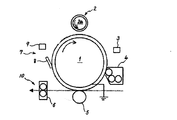
<画像形成方法及び装置について>
以下、本発明が適用される画像形成装置について実施形態を説明する。但し、これらはその一例であって、これに限定されるものではない。図7に、後述する各実施例にも共通した構成を有する画像形成装置の一例を示す。この画像形成装置は、有機感光体からなる電子写真感光体を備えている。電子写真感光体1は、少なくとも感光層を有し、感光体表面に平均粒子径20nm以下のカーボンを主成分とするナノ微粒子を有する膜であることを特徴としている。
<Image Forming Method and Apparatus>
Embodiments of an image forming apparatus to which the present invention is applied will be described below. However, these are just examples, and the present invention is not limited to these. FIG. 7 shows an example of an image forming apparatus having a configuration common to the embodiments described later. This image forming apparatus includes an electrophotographic photosensitive member made of an organic photosensitive member. The electrophotographic photoreceptor 1 is characterized in that it is a film having at least a photosensitive layer and nano-particles mainly composed of carbon having an average particle diameter of 20 nm or less on the surface of the photoreceptor.
<全体構成について>
図7において電子写真感光体1は、図示しない駆動装置により回転駆動され、その表面が近接帯電方式の帯電装置2の帯電ローラ2aにより所定の極性に帯電される。帯電された電子写真感光体1の表面は、露光装置3によって露光され画像情報に応じた静電潜像が形成される。この静電潜像は、現像装置4から電子写真感光体1の表面に供給される現像剤としてのトナーにより現像されて、トナー像として可視像化される。
<About the overall configuration>
In FIG. 7, the electrophotographic photosensitive member 1 is rotationally driven by a driving device (not shown), and the surface thereof is charged to a predetermined polarity by a charging
一方、図示しない給紙部からは記録媒体としての転写紙が電子写真感光体1に向けて給送される。この転写紙には、電子写真感光体1に対向配置されている転写装置5によって電子写真感光体1上のトナー像が転写紙上に転写される。トナー像が転写された転写紙は、電子写真感光体1から分離した後、転写材搬送経路10に沿って定着装置6に搬送されて、トナー像が定着される。 On the other hand, a transfer sheet as a recording medium is fed toward the electrophotographic photosensitive member 1 from a paper feeding unit (not shown). A toner image on the electrophotographic photosensitive member 1 is transferred onto the transfer paper on the transfer paper by a transfer device 5 disposed opposite to the electrophotographic photosensitive member 1. The transfer paper onto which the toner image has been transferred is separated from the electrophotographic photosensitive member 1 and then conveyed to the fixing device 6 along the transfer material conveyance path 10 to fix the toner image.
転写紙にトナー像を転写した後の電子写真感光体1上に残留している残留トナーとしての転写残トナーは、クリーニング装置7のクリーニングブレード8によって電子写真感光体1上から除去される。また、転写残トナーが除去された後の電子写真感光体表面の残留電荷は、除電装置9により除去される。このようにして、電子写真感光体1は繰り返し使用される Transfer residual toner as residual toner remaining on the electrophotographic photosensitive member 1 after the toner image is transferred to the transfer paper is removed from the electrophotographic photosensitive member 1 by the cleaning blade 8 of the cleaning device 7. Further, the residual charge on the surface of the electrophotographic photosensitive member after the transfer residual toner is removed is removed by the static eliminator 9. In this way, the electrophotographic photoreceptor 1 is repeatedly used.
また、本実施形態の画像形成装置では、電子写真感光体、帯電部材、現像装置、クリーニング装置が一体に構成され、画像形成装置本体から着脱可能なプロセスカートリッジとして構成されている。 In the image forming apparatus according to the present embodiment, the electrophotographic photosensitive member, the charging member, the developing device, and the cleaning device are integrally configured as a process cartridge that is detachable from the image forming apparatus main body.
<帯電について>
次に画像形成装置に用いる帯電装置2について説明する。この帯電装置2は、近接放電を用いて電子写真感光体を帯電する。近接放電を用いて電子写真感光体を帯電する方法としては、回動可能なローラ状の帯電部材(以下、帯電ローラという)2aを電子写真感光体に接触させて配置する接触帯電方式と、帯電ローラを電子写真感光体に非接触に配置する非接触帯電方式とがある。本実施形態においては、非接触帯電方式を用いている。
<About charging>
Next, the charging
本発明は接触帯電方式にも適用できるが、接触帯電方式においては電子写真感光体表面との接触性を向上させ、かつ電子写真感光体に機械的ストレスを与えない弾性部材を用いる事が好ましい。しかし弾性部材を用いた場合には帯電ニップ幅が広くなり、これによって帯電ローラ側に保護物質が付着しやすくなることがある。よって、高耐久化の為には、非接触帯電方式を採用する方が有利である。本実施形態1においては、電子写真感光体表面における少なくとも画像形成領域に対して所定の帯電ギャップをもって対向するよう帯電ローラ2aを配置した非接触帯電方式を採用した。
The present invention can also be applied to a contact charging method. However, in the contact charging method, it is preferable to use an elastic member that improves the contact property with the surface of the electrophotographic photosensitive member and does not apply mechanical stress to the electrophotographic photosensitive member. However, when an elastic member is used, the charging nip width is widened, which may cause the protective material to easily adhere to the charging roller side. Therefore, it is more advantageous to adopt a non-contact charging method for high durability. The first embodiment employs a non-contact charging method in which the charging
図8は、本実施形態1の画像形成装置に用いる帯電装置2の説明図である。
帯電ローラ21は軸部21aとローラ部21bとからなる。ローラ部21bは軸部21aの回転によって回動可能であり、電子写真感光体1表面のうち画像が形成される画像形成領域11に対向する部分は電子写真感光体1と非接触である。帯電ローラ21は、その長手方向(軸方向)の寸法が画像形成領域よりも少し長く設定されており、その長手方向の両端部にスペーサ22を設けている。これら2つのスペーサ22を電子写真感光体1表面両端部の非画像形成領域12に当接させることによって、電子写真感光体1と帯電ローラとの間に微小なギャップ14を形成している。
FIG. 8 is an explanatory diagram of the
The charging
この微小なギャップ14は、帯電ローラ21と電子写真感光体1との最近接部における距離が1〜100μmに維持できるよう構成している。このギャップ14のより好ましい範囲は、10〜80μm、さらに好ましくは30〜65μmであり、本実施形態1の装置では、50μmに設定した。また、軸部21aをスプリングからなる加圧バネ15によって電子写真感光体側に加圧している。これにより、微小なギャップ14を精度よく維持することができる。また、帯電ローラ21はスペーサ22を介して電子写真感光体表面に連れ回って回転する。
The
帯電ローラ21には帯電用の電源16が接続されている。これにより、電子写真感光体表面と帯電ローラ表面との間の微小な空隙での近接放電により、電子写真感光体表面を均一に帯電する。印加電圧としては直流電圧に交流電圧を重畳し使用する。印加電圧として直流電圧に交流電圧を重畳させた交番電圧を使用すると、微小ギャップ変動による帯電電位のばらつきなどの影響が抑制されて均一な帯電が可能となる。本実施形態1においては直流成分である直流電圧に交流成分である交流電圧を重畳した交番電圧を用いている。
A charging
帯電ローラ21は円柱状を呈する導電性支持体としての芯金と、芯金の外周面上に形成された抵抗調整層を有する。帯電ローラ21の表面は硬質であることが望ましい。ローラ部材としてはゴム部材も使用できるが、ゴム部材のように変形しやすい部材であると電子写真感光体1との微小ギャップ14の均一な維持が困難となり、作像条件によっては帯電ローラ21の中央部のみが電子写真感光体表面に突発的に接触する可能性がある。帯電ローラ21は、非接触帯電方式を使用する場合にはたわみが少ない硬質の部材が望ましい。
The charging
表面が硬質な帯電ローラ21の具体例としては、例えば、抵抗調整層を高分子型イオン導電剤が分散する熱可塑性樹脂組成物(ポリエチレン、ポリプロピレン、ポリメタクリル酸メチル、ポリスチレン及びその共重合体等)により形成し、抵抗調整層の表面を硬化剤により硬化皮膜処理されたものが挙げられる。また硬化皮膜処理は、例えば、イソシアネート含有化合物を含む処理溶液に抵抗調整層を浸漬させることにより行われるが、抵抗調整層の表面に改めて硬化処理皮膜層を形成することにより行われてもよい。本実施形態では、帯電ローラ2aをφ10mm(直径10mm)で形成した。
Specific examples of the charging
以上の説明から明らかなように、本発明の電子写真感光体は電子写真複写機に利用するのみならず、レーザービームプリンター、CRTプリンター、LEDプリンター、液晶プリンター及びレーザー製版等の電子写真応用分野にも広く用いることができるものである。 As is apparent from the above description, the electrophotographic photosensitive member of the present invention is not only used in electrophotographic copying machines, but also in electrophotographic application fields such as laser beam printers, CRT printers, LED printers, liquid crystal printers, and laser plate making. Can also be used widely.
以下本発明を実施例により説明するが、これにより本発明の態様が限定されるものではない。部はいずれも重量基準である。 Hereinafter, the present invention will be described with reference to examples, but the present invention is not limited thereto. All parts are by weight.
[実施例1]
Al製支持体(外径30mmφ)に、下記の組成の下引き層用塗工液を乾燥後の膜厚が28μmになるように浸漬法で塗工し、下引き層を形成した。
[Example 1]
An undercoat layer coating solution was applied to an Al support (outer diameter: 30 mmφ) by an immersion method so that the film thickness after drying was 28 μm to form an undercoat layer.
<下引き層用塗工液>
アルキッド樹脂 6部
(ベッコゾール1307−60−EL、大日本インキ化学工業製)
メラミン樹脂 4部
(スーパーベッカミン G−821−60、大日本インキ化学工業製)
酸化チタン 40部
(CR−EL:石原産業)
メチルエチルケトン 50部
<Coating liquid for undercoat layer>
Alkyd resin 6 parts (Beckosol 1307-60-EL, manufactured by Dainippon Ink & Chemicals, Inc.)
Melamine resin 4 parts (Super Becamine G-821-60, manufactured by Dainippon Ink & Chemicals, Inc.)
40 parts of titanium oxide
(CR-EL: Ishihara Sangyo)
50 parts of methyl ethyl ketone
この下引き層上にビスアゾ顔料を含む下記の組成の電荷発生層塗工液を浸漬塗工し、加熱乾燥させ、膜厚0.2μmの電荷発生層を形成した。 On this undercoat layer, a charge generation layer coating solution having the following composition containing a bisazo pigment was dip coated and dried by heating to form a 0.2 μm thick charge generation layer.
<電荷発生層用塗工液>
下記化学式1のビスアゾ顔料 2.5部
ポリビニルブチラール(XYHL、UCC製) 0.5部
シクロヘキサノン 200部
メチルエチルケトン 80部
<Coating liquid for charge generation layer>
Bisazo pigment of the following chemical formula 2.5 2.5 parts polyvinyl butyral (XYHL, manufactured by UCC) 0.5

この電荷発生層上に下記の組成の電荷輸送層用塗工液を用いて、浸積塗工し、加熱乾燥させ、膜厚22μmの電荷輸送層とした。 On this charge generation layer, a charge transport layer coating solution having the following composition was dip-coated and dried by heating to obtain a charge transport layer having a thickness of 22 μm.
<電荷輸送層用塗工液>
ビスフェーノルZ型ポリカーボネート 10部
下記化学式2の電荷輸送物質 10部
テトラヒドロフラン 80部
1%シリコーンオイルのテトラヒドロフラン溶液 0.2部
(KF50、信越化学工業製)
<Coating liquid for charge transport layer>
Bisphenol N-type polycarbonate 10 parts Charge transport material of the following
この電荷輸送層上に下記の組成の表面層用塗工液を用いて、スプレー塗工し、150℃加熱乾燥させ、膜厚5.0μmの表面層とした。
<表面層用塗工液>
電荷輸送層に用いた電荷輸送物質
ビスフェーノルZ型ポリカーボネート
ダイヤモンド微粒子
(ナノダイヤモンド、平均粒径4〜8nm、北京国瑞昇科技有限公司)
テトラヒドロフラン
シクロヘキサノン
(混合比(重量))
電荷輸送物質/ポリカーボネート/ダイヤモンド微粒子/テトラヒドロフラン/シクロヘキサノン=4.5/5/0.5/170/50
On this charge transport layer, a surface layer coating solution having the following composition was spray coated and dried by heating at 150 ° C. to form a surface layer having a thickness of 5.0 μm.
<Coating liquid for surface layer>
Charge transport material used for charge transport layer
Bisphenol A-type polycarbonate diamond fine particles (Nanodiamond, average particle size 4-8nm, Beijing National Rising Technology Co., Ltd.)
Tetrahydrofuran cyclohexanone
(Mixing ratio (weight))
Charge transport material / polycarbonate / diamond fine particles / tetrahydrofuran / cyclohexanone = 4.5 / 5 / 0.5 / 170/50
[実施例2]
実施例1に用いたダイヤモンド微粒子の代わりに下記カーボン微粒子を添加すること以外は全て実施例1と同様にして作製した。
カーボン微粒子(カーボンブラックHCF#2600、平均粒径13nm、三菱化学)
[Example 2]
It was produced in the same manner as in Example 1 except that the following carbon fine particles were added in place of the diamond fine particles used in Example 1.
Carbon fine particles (carbon black HCF # 2600, average particle size 13 nm, Mitsubishi Chemical)
[実施例3]
実施例1に用いたダイヤモンド微粒子の代わりに下記カーボン粒子を添加すること以外は全て実施例1と同様にして作製した。
カーボン微粒子(カーボンブラックMCF88、平均粒径18nm、三菱化学)
[Example 3]
It was produced in the same manner as in Example 1 except that the following carbon particles were added instead of the diamond fine particles used in Example 1.
Carbon fine particles (carbon black MCF88, average particle size 18nm, Mitsubishi Chemical)
[比較例1]
表面層を設けないこと以外は全て実施例1と同様にして作製した。
[Comparative Example 1]
All were produced in the same manner as in Example 1 except that the surface layer was not provided.
[比較例2]
表面層中にダイヤモンド微粒子を添加しないこと以外は全て実施例1と同様にして作製した。
[Comparative Example 2]
It was produced in the same manner as Example 1 except that diamond fine particles were not added to the surface layer.
[比較例3]
実施例1に用いたダイヤモンド微粒子の代わりに下記カーボン微粒子を添加すること以外は全て実施例1と同様にして作製した。
カーボン微粒子(カーボンブラックLFM MA−8、平均粒径24nm、三菱化学)
[Comparative Example 3]
It was produced in the same manner as in Example 1 except that the following carbon fine particles were added in place of the diamond fine particles used in Example 1.
Carbon fine particles (carbon black LFM MA-8, average particle size 24 nm, Mitsubishi Chemical)
[比較例4]
実施例1に用いたダイヤモンド微粒子の代わりに下記カーボン微粒子を添加すること以外は全て実施例1と同様にして作製した。
カーボン微粒子(カーボンブラックLFM MA220、平均粒径55nm、三菱化学)
[Comparative Example 4]
It was produced in the same manner as in Example 1 except that the following carbon fine particles were added in place of the diamond fine particles used in Example 1.
Carbon fine particles (carbon black LFM MA220, average particle size 55 nm, Mitsubishi Chemical)
[実施例4]
実施例1の表面層塗工液の代わりに下記塗工液および製膜方法を使用すること以外は、全て実施例1と同様にして作製した。
[Example 4]
It was produced in the same manner as in Example 1 except that the following coating solution and film forming method were used instead of the surface layer coating solution in Example 1.
<表面層塗工液>
電荷輸送性構造を有さない3官能以上のラジカル重合性モノマー 10部
(KAYARAD TMPTA:日本化薬製)
下記化学式3の1官能の電荷輸送性構造を有するラジカル重合性化合物 9部
光重合開始剤 0.5部
1−ヒドロキシ−シクロヘキシル−フェニル−ケトン
(イルガキュア184、チバ・スペシャルティ・ケミカルズ製)
ダイヤモンド微粒子 1部
(ナノダイヤモンド、平均粒径4〜8nm、北京国瑞昇科技有限公司)
テトラヒドロフラン 80部
スプレー塗工後、UV照射を行い、加熱乾燥(130℃、20分)を行った。
<Surface layer coating solution>
10 parts of radically polymerizable monomer having 3 or more functional groups not having a charge transporting structure (KAYARAD TMPTA: manufactured by Nippon Kayaku)
Radical polymerizable compound having a monofunctional charge transport structure of the following
Diamond fine particles 1 part (Nanodiamond, average particle size 4-8nm, Beijing National Rising Technology Co., Ltd.)
Tetrahydrofuran 80 parts After spray coating, UV irradiation was performed, followed by heat drying (130 ° C., 20 minutes).
[比較例5]
表面層中にダイヤモンド微粒子を添加しないこと以外は全て実施例5と同様にして作製した。
[Comparative Example 5]
All were produced in the same manner as in Example 5 except that diamond fine particles were not added to the surface layer.
(実機通紙試験)
作製した電子写真感光体を、直流成分に交流成分を重畳した電圧を印加する非接触帯電機を有するリコー製IPSiO Color CX9000を用いて、実機通紙試験(A4、NBSリコー製My Paper、スタート時感光体表面帯電電位−650V)を実施し、摩耗特性、画像(S3チャート)特性評価を行った。結果を表1、2、3、4に示す。
また直流成分のみの電圧を印加する接触帯電器に改造したリコー製IPSiO Color CX9000を用いて、実機通紙試験(A4、NBSリコー製My Paper、スタート時感光体表面帯電電位−700V)を実施し、摩耗特性を評価した。結果を表5、6に示す。
(Real machine paper test)
Using the Ricoh IPSiO Color CX9000 having a non-contact charging device that applies a voltage in which an alternating current component is superimposed on a direct current component, the produced electrophotographic photosensitive member is tested using an actual machine (A4, My Paper manufactured by NBS Ricoh, at start). Photoreceptor surface charging potential -650 V) was performed, and wear characteristics and image (S3 chart) characteristics were evaluated. The results are shown in Tables 1, 2, 3, and 4.
Also, using a Ricoh IPSiO Color CX9000 modified to a contact charger that applies only a DC component voltage, an actual paper feeding test (A4, NBS Ricoh My Paper, photoreceptor surface charging potential at start-700 V) was performed. The wear characteristics were evaluated. The results are shown in Tables 5 and 6.
本発明の電子写真感光体は、直流電圧に交流電圧を重畳した近接放電による帯電方式を採用する画像形成装置における電子写真感光体として好適に用いることができる。 The electrophotographic photoreceptor of the present invention can be suitably used as an electrophotographic photoreceptor in an image forming apparatus that employs a charging method based on proximity discharge in which an alternating voltage is superimposed on a direct current voltage.
1 電子写真感光体
2 帯電装置
2a 帯電ローラ
3 露光装置
4 現像装置
5 転写装置
6 定着装置
7 クリーニング装置
8 クリーニングブレード
9 除電装置
10 転写材搬送経路
11 画像形成領域
12 非画像形成領域
14 ギャップ
15 加圧バネ
16 電源
21 帯電ローラ
21a 軸部
21b ローラ部
22 スペーサ
DESCRIPTION OF SYMBOLS 1 Electrophotographic
Claims (11)
Priority Applications (1)
| Application Number | Priority Date | Filing Date | Title |
|---|---|---|---|
| JP2005013742A JP2006201542A (en) | 2005-01-21 | 2005-01-21 | Electrophotographic photoreceptor and image forming method using the same |
Applications Claiming Priority (1)
| Application Number | Priority Date | Filing Date | Title |
|---|---|---|---|
| JP2005013742A JP2006201542A (en) | 2005-01-21 | 2005-01-21 | Electrophotographic photoreceptor and image forming method using the same |
Publications (1)
| Publication Number | Publication Date |
|---|---|
| JP2006201542A true JP2006201542A (en) | 2006-08-03 |
Family
ID=36959581
Family Applications (1)
| Application Number | Title | Priority Date | Filing Date |
|---|---|---|---|
| JP2005013742A Pending JP2006201542A (en) | 2005-01-21 | 2005-01-21 | Electrophotographic photoreceptor and image forming method using the same |
Country Status (1)
| Country | Link |
|---|---|
| JP (1) | JP2006201542A (en) |
Cited By (1)
| Publication number | Priority date | Publication date | Assignee | Title |
|---|---|---|---|---|
| JP2008261971A (en) * | 2007-04-11 | 2008-10-30 | Ricoh Co Ltd | Electrophotographic photoreceptor, and image forming method, image forming apparatus and process cartridge for image forming apparatus using the same |
-
2005
- 2005-01-21 JP JP2005013742A patent/JP2006201542A/en active Pending
Cited By (1)
| Publication number | Priority date | Publication date | Assignee | Title |
|---|---|---|---|---|
| JP2008261971A (en) * | 2007-04-11 | 2008-10-30 | Ricoh Co Ltd | Electrophotographic photoreceptor, and image forming method, image forming apparatus and process cartridge for image forming apparatus using the same |
Similar Documents
| Publication | Publication Date | Title |
|---|---|---|
| JP4144755B2 (en) | Electrophotographic photosensitive member, image forming method using the same, image forming apparatus, and process cartridge for image forming apparatus | |
| JP4194973B2 (en) | Electrophotographic photosensitive member, image forming method using the same, image forming apparatus, and process cartridge for image forming apparatus | |
| JP4248483B2 (en) | Electrophotographic photosensitive member, method for producing the same, image forming method using the same, image forming apparatus, and process cartridge for image forming apparatus | |
| JP4987546B2 (en) | Electrophotographic photosensitive member, image forming method using the same, image forming apparatus, and process cartridge for image forming apparatus | |
| JP6056256B2 (en) | Electrophotographic photoreceptor, image forming apparatus having the photoreceptor, image forming method, process cartridge, and electrophotographic photoreceptor surface layer coating solution | |
| JP2007279678A (en) | Electrophotographic photoreceptor and image forming method using same, and image forming apparatus and process cartridge therefor | |
| JP2007079244A (en) | Image forming apparatus, process cartridge and image forming method | |
| JP2006010757A (en) | Electrophotographic photoreceptor, method for manufacturing same, image forming method using same, image forming apparatus and process cartridge for image forming apparatus | |
| JP2007272191A (en) | Electrophotographic photoreceptor and image forming method using the same, image forming apparatus and process cartridge for image forming apparatus | |
| JP2007272192A (en) | Electrophotographic photoreceptor and image forming method using the same, image forming apparatus and process cartridge for image forming apparatus | |
| JP4216228B2 (en) | Electrophotographic photosensitive member, image forming method using the same, image forming apparatus, and process cartridge for image forming apparatus | |
| JP4712351B2 (en) | Electrophotographic photosensitive member, image forming method using the same, image forming apparatus, and process cartridge for image forming apparatus | |
| JP4118839B2 (en) | Electrophotographic photosensitive member, image forming method using the same, image forming apparatus, and process cartridge for image forming apparatus | |
| JP2007322483A (en) | Electrophotographic photoreceptor, image forming method and image forming apparatus using the same, and process cartridge for image forming apparatus | |
| JP2006234943A (en) | Electrophotographic photoreceptor, image forming apparatus, process cartridge, and image forming method | |
| JP4118258B2 (en) | Electrophotographic photosensitive member, image forming method using the same, image forming apparatus, and process cartridge for image forming apparatus | |
| JP4195418B2 (en) | Electrophotographic photoreceptor, method for producing the same, image forming method using the same, image forming apparatus, and process cartridge for image forming apparatus | |
| JP2005077947A (en) | Electrophotographic photoreceptor, process cartridge and electrophotographic apparatus | |
| JP4532366B2 (en) | Image forming apparatus, image forming method, and process cartridge | |
| JP4420397B2 (en) | Electrophotographic photosensitive member, image forming apparatus, and process cartridge for image forming apparatus | |
| JP2006201542A (en) | Electrophotographic photoreceptor and image forming method using the same | |
| JP5532393B2 (en) | Electrophotographic photosensitive member, image forming method using the same, image forming apparatus, and process cartridge for image forming apparatus | |
| JP5038839B2 (en) | Image carrier, image forming method using the same, image forming apparatus, and process cartridge for image forming apparatus | |
| JP4335645B2 (en) | Image forming method, image forming apparatus, and process cartridge for image forming apparatus | |
| JP4785648B2 (en) | Image forming method |
Legal Events
| Date | Code | Title | Description |
|---|---|---|---|
| A621 | Written request for application examination |
Effective date: 20071126 Free format text: JAPANESE INTERMEDIATE CODE: A621 |
|
| A977 | Report on retrieval |
Free format text: JAPANESE INTERMEDIATE CODE: A971007 Effective date: 20090522 |
|
| A131 | Notification of reasons for refusal |
Free format text: JAPANESE INTERMEDIATE CODE: A131 Effective date: 20090615 |
|
| A521 | Written amendment |
Effective date: 20090803 Free format text: JAPANESE INTERMEDIATE CODE: A523 |
|
| A131 | Notification of reasons for refusal |
Effective date: 20090930 Free format text: JAPANESE INTERMEDIATE CODE: A131 |
|
| A02 | Decision of refusal |
Effective date: 20100202 Free format text: JAPANESE INTERMEDIATE CODE: A02 |