JP2006184673A - Liquid crystal device and electronic apparatus - Google Patents
Liquid crystal device and electronic apparatus Download PDFInfo
- Publication number
- JP2006184673A JP2006184673A JP2004379206A JP2004379206A JP2006184673A JP 2006184673 A JP2006184673 A JP 2006184673A JP 2004379206 A JP2004379206 A JP 2004379206A JP 2004379206 A JP2004379206 A JP 2004379206A JP 2006184673 A JP2006184673 A JP 2006184673A
- Authority
- JP
- Japan
- Prior art keywords
- liquid crystal
- light
- substrate
- optical axis
- crystal device
- Prior art date
- Legal status (The legal status is an assumption and is not a legal conclusion. Google has not performed a legal analysis and makes no representation as to the accuracy of the status listed.)
- Withdrawn
Links
Images


Landscapes
- Liquid Crystal (AREA)
- Projection Apparatus (AREA)
Abstract
Description
本発明は液晶装置及び電子機器に係り、特に、電界無印加状態で液晶が基板の内面に対して実質的に垂直に配向する垂直配向モードの液晶装置に関する。 The present invention relates to a liquid crystal device and an electronic apparatus, and more particularly to a vertical alignment mode liquid crystal device in which liquid crystal is aligned substantially perpendicular to the inner surface of a substrate in the absence of an electric field.
従来の液晶装置は、一般に、一対の基板間に液晶を封入したセル構造を有し、この液晶の配向状態を電界によって制御することで光を変調するように構成されている。このような液晶装置としては、電界無印加状態で液晶の配向方向が液晶層の厚さ方向に90度捩れ、電界印加状態で液晶が基板の内面に対して略垂直に配向するTNモードの液晶装置や、電界の有無で液晶の配向方向が基板の内面と平行な平面上を旋回するIPSモードの液晶装置などがあるが、TNモードでは視野角が狭いという問題点があり、また、IPSモードでは視野角を比較的広く確保できるものの、応答速度が遅い、光透過率が不十分である、製造が難しいなどの問題点がある。 Conventional liquid crystal devices generally have a cell structure in which liquid crystal is sealed between a pair of substrates, and are configured to modulate light by controlling the alignment state of the liquid crystal by an electric field. As such a liquid crystal device, a TN mode liquid crystal in which the alignment direction of the liquid crystal is twisted 90 degrees in the thickness direction of the liquid crystal layer when no electric field is applied, and the liquid crystal is aligned substantially perpendicular to the inner surface of the substrate when the electric field is applied. There are devices and IPS mode liquid crystal devices in which the alignment direction of the liquid crystal rotates on a plane parallel to the inner surface of the substrate in the presence or absence of an electric field, but there is a problem that the viewing angle is narrow in the TN mode. However, although a wide viewing angle can be secured, there are problems such as a slow response speed, insufficient light transmittance, and difficulty in manufacturing.
そこで、広い視野角を確保しつつ、その他の特性をも満足することのできる方式として、VA(Vertical Aligned)モードの液晶表示装置が開発されている。この液晶装置は、一般的には誘電異方性が負の液晶を用い、電圧無印加状態で液晶が基板の内面に対して略垂直に配向し、電圧印加状態で液晶が倒れて基板の内面に対して略平行に配向するように構成される。このVAモードの液晶装置の欠点は、電界印加状態において液晶の倒れる方位角を制御することが難しいことにある。液晶の方位角は光学特性に大きな影響を与えるため、通常、初期配向状態において液晶が所定の方位に向けて僅かに傾斜した状態、すなわち、90度未満のプレチルト角を有するように構成され、このプレチルト角の方位角を予め規定することで、液晶の倒れる方位を制御するようにしている。 Therefore, a VA (Vertical Aligned) mode liquid crystal display device has been developed as a method that can satisfy other characteristics while ensuring a wide viewing angle. This liquid crystal device generally uses a liquid crystal having a negative dielectric anisotropy, and the liquid crystal is oriented substantially perpendicularly to the inner surface of the substrate when no voltage is applied. It is comprised so that it may orientate substantially parallel to. The drawback of this VA mode liquid crystal device is that it is difficult to control the azimuth angle at which the liquid crystal tilts when an electric field is applied. Since the azimuth angle of the liquid crystal has a great influence on the optical characteristics, it is usually configured so that the liquid crystal is slightly tilted toward a predetermined orientation in the initial alignment state, that is, has a pretilt angle of less than 90 degrees. By predefining the azimuth angle of the pretilt angle, the azimuth direction of the liquid crystal is controlled.
また、直視型の液晶表示装置では、液晶の方位角が偏ると視角依存性が生ずるため、通常、基板の内面に突起やスリット(電極パターンの開口部)などの配向制御構造を形成し、これらの配向制御構造によって液晶の倒れる方位が偏らないように構成して視角依存性を低減させている(例えば、以下の特許文献1参照)。 In direct-view liquid crystal display devices, viewing angle dependence occurs when the azimuth angle of the liquid crystal is deviated. Therefore, alignment control structures such as protrusions and slits (electrode pattern openings) are usually formed on the inner surface of the substrate. The orientation control structure is configured so that the orientation in which the liquid crystal falls is not biased to reduce the viewing angle dependency (see, for example, Patent Document 1 below).
さらに、画素領域を複数のサブドットに分割し、これらのサブドット毎に上記の配向制御構造(突起及び電極の開口部)を設けることにより、配向制御構造による画素内の液晶の配向状態の制御性を高める方法も提案されている(例えば、以下の特許文献2及び3参照)。この構造では、上記に加えて、サブドットの形状を円形や正方形などの回転対象形状とすることでさらに配向制御性を向上させ、また、液晶にカイラル剤を添加することで配向不良(ディスクリネーション)に起因するざらしみ(視角によって表示態様が変化するしみ)などの表示不良の発生を防止している。
Furthermore, the pixel region is divided into a plurality of subdots, and the alignment control structure (protrusions and electrode openings) is provided for each subdot, thereby controlling the alignment state of the liquid crystal in the pixel by the alignment control structure. A method for improving the performance has also been proposed (see, for example,
一方、液晶装置においては、所望の表示態様や投射画像などを形成するために、縦横にマトリクス状に複数の画素を配列させた構造が一般的であるが、これらの画素間には光が透過しない遮光領域が設けられ、この遮光領域が液晶装置の開口率を低下させ、表示や画像の明るさを減少させるという問題がある。特に、画素毎にスイッチング素子を備えたアクティブマトリクス型の液晶装置では、スイッチング素子の設けられた領域を遮光する必要があるために上記開口率がさらに低下し、また、半透過反射型の液晶装置では、透過型表示と反射型表示の双方を実現可能とするために開口率が大幅に低下するという問題がある。そこで、この問題を解決する方法として、液晶装置の上記画素に対応させた集光レンズを備えたマイクロレンズアレイを作り込み、このマイクロレンズアレイの各集光レンズによって入射光を集光して画素内に導入することで、実質的に構造上の開口率を高める場合と同様の効果が得られるようにする方法が知られている(例えば、以下の特許文献4参照)。
しかしながら、液晶ライトバルブでは画素自体が小さいために、上記のリブやスリットの作製が困難であり、作製できたとしても、開口率の低下や、かつ画素間の電界の影響を受け、期待される配向制御が困難である。また、上記従来の垂直配向モードの液晶装置では、液晶分子が初期配向状態において90度未満のプレチルト角を有することによって基板法線に対して僅かではあるが傾斜しているので、液晶層への光の入射方向と、液晶分子の長軸方向とが僅かに異なるものとなり、電界無印加時に光透過状態となるように構成した場合には光透過率が低下し、電圧無印加時に光遮断状態となるように構成した場合には光漏れが生ずるという問題点がある。 However, since the pixels themselves are small in the liquid crystal light valve, it is difficult to produce the ribs and slits described above, and even if they can be produced, they are expected to be affected by a decrease in the aperture ratio and the influence of the electric field between the pixels. It is difficult to control the orientation. Further, in the conventional vertical alignment mode liquid crystal device, since the liquid crystal molecules have a pretilt angle of less than 90 degrees in the initial alignment state, the liquid crystal molecules are slightly tilted with respect to the substrate normal line. The light incident direction is slightly different from the major axis direction of the liquid crystal molecules, and when configured to be in a light transmissive state when no electric field is applied, the light transmittance decreases, and the light is blocked when no voltage is applied. However, there is a problem that light leakage occurs.
また、上記のマイクロレンズアレイを備えた液晶装置では、光入射側の基板の内面に凹部を形成することによって液晶分子のプレチルトの方位角が放射状になるように構成するとともに、この凹部に対応する凸部を光入射側の基板の外面に形成することで、上記凹部の内面にほぼ垂直に配向した液晶分子の長軸方向と入射光の入射方向とが平行になる態様で入射光が集光され、その結果、高いコントラストを得ることができるとされている。しかし、基板内面上の凹部と基板外面上の凸部とを対応する形状に形成することは極めて困難であり、実際には高精度の光学系を構成することはできないとともに、液晶分子は基板内面に対して完全に垂直に配向する(すなわち、プレチルト角が90度になる)のではなく、ある程度傾斜した状態で配向する(すなわち、プレチルト角が90度未満になる)ので、仮に光学系を高精度に形成できたとしても、十分な効果を得ることができず、光学補償板などを補助的に用いる必要がある。 Further, in the liquid crystal device provided with the microlens array, a recess is formed on the inner surface of the substrate on the light incident side so that the azimuth angle of the pretilt of the liquid crystal molecules becomes radial and corresponds to the recess. By forming the convex portion on the outer surface of the substrate on the light incident side, the incident light is condensed in such a manner that the major axis direction of the liquid crystal molecules aligned substantially perpendicular to the inner surface of the concave portion is parallel to the incident light incident direction. As a result, it is said that high contrast can be obtained. However, it is extremely difficult to form the concave portion on the inner surface of the substrate and the convex portion on the outer surface of the substrate in a corresponding shape. In fact, a high-precision optical system cannot be formed, and the liquid crystal molecules are formed on the inner surface of the substrate. Rather than being oriented completely perpendicular to (i.e., the pretilt angle is 90 degrees), rather than being tilted to some extent (i.e., the pretilt angle is less than 90 degrees), Even if it can be formed accurately, a sufficient effect cannot be obtained, and an optical compensator or the like needs to be used as an auxiliary.
そこで、本発明は上記問題点を解決するものであり、その課題は、垂直配向モードの液晶装置において、初期配向状態における透過率の低下或いは光漏れを抑制することにより、従来よりも高いコントラストを実現できる構成を提供することにある。 Therefore, the present invention solves the above-mentioned problems, and the problem is that in a vertical alignment mode liquid crystal device, a lower contrast in the initial alignment state or light leakage is suppressed, thereby providing a higher contrast than conventional. It is to provide a configuration that can be realized.
斯かる実情に鑑み、本発明の液晶装置は、一対の基板、該一対の基板間に配置された液晶層、及び、前記液晶層に電界を印加するための電界印加構造を有し、電界無印加時において前記液晶層内の液晶分子が実質的に基板法線方向に配向される初期配向状態を備えた液晶装置において、前記初期配向状態において前記液晶分子が90度未満のプレチルト角を有し、かつ、少なくとも前記基板面内の所定範囲内において前記液晶分子のプレチルトの方位角が実質的に揃うように構成され、少なくとも前記基板面内の前記所定範囲内において前記基板法線方向から入射する光の光軸を前記液晶分子の前記プレチルト角の前記方位角側に傾斜させる光軸偏向手段を具備することを特徴とする。 In view of such circumstances, the liquid crystal device of the present invention has a pair of substrates, a liquid crystal layer disposed between the pair of substrates, and an electric field application structure for applying an electric field to the liquid crystal layer, In the liquid crystal device having an initial alignment state in which the liquid crystal molecules in the liquid crystal layer are substantially aligned in the normal direction of the substrate during heating, the liquid crystal molecules have a pretilt angle of less than 90 degrees in the initial alignment state. And, the azimuth angle of the pretilt of the liquid crystal molecules is substantially aligned at least within a predetermined range within the substrate surface, and is incident from the normal direction of the substrate at least within the predetermined range within the substrate surface. An optical axis deflecting means for tilting the optical axis of light toward the azimuth side of the pretilt angle of the liquid crystal molecules is provided.
この発明によれば、少なくとも所定範囲内において液晶分子のプレチルトの方位角が実質的に揃うように構成されていて、この少なくとも所定範囲内において光軸偏向手段が基板法線方向に入射する光の光軸を液晶層内にて液晶分子のプレチルトの方位角側に傾斜させることにより、初期配向状態において入射光の光軸が液晶分子の長軸方向に近づくように構成できるので、初期配向状態が光透過状態に対応している場合には光透過率の低下を抑制することができ、また、初期配向状態が光遮断状態に対応している場合には光漏れを抑制することが可能になるため、液晶装置のコントラストを高めることができる。 According to the present invention, the azimuth angles of the pretilts of the liquid crystal molecules are substantially aligned at least within a predetermined range, and the optical axis deflecting means is at least within the predetermined range and the optical axis deflecting means is incident on the substrate normal direction. By tilting the optical axis toward the azimuth side of the pretilt of the liquid crystal molecules in the liquid crystal layer, the optical axis of the incident light can be configured to approach the major axis direction of the liquid crystal molecules in the initial alignment state. When it corresponds to the light transmission state, a decrease in light transmittance can be suppressed, and when the initial alignment state corresponds to the light blocking state, light leakage can be suppressed. Therefore, the contrast of the liquid crystal device can be increased.
本発明において、前記光軸偏向手段は、前記プレチルト角と実質的に対応する角度に前記光軸を傾斜させることが好ましい。これによれば、液晶分子の長軸方向に対して光軸を実質的に平行に設定することができるため、コントラストをさらに高めることができる。 In the present invention, it is preferable that the optical axis deflecting unit tilts the optical axis at an angle substantially corresponding to the pretilt angle. According to this, since the optical axis can be set substantially parallel to the major axis direction of the liquid crystal molecules, the contrast can be further enhanced.
本発明において、前記光軸偏向手段は、前記液晶層に対して光入射側に配置された光屈折素子で構成されていることが好ましい。これによれば、液晶層の光入射側にプリズム等の光屈折素子を設けることにより、基板法線方向に対して光軸を容易かつ確実に傾斜させることができる。 In the present invention, it is preferable that the optical axis deflecting unit is composed of a photorefractive element disposed on the light incident side with respect to the liquid crystal layer. According to this, by providing a photorefractive element such as a prism on the light incident side of the liquid crystal layer, the optical axis can be easily and reliably inclined with respect to the normal direction of the substrate.
本発明において、前記光軸偏向手段は、前記液晶層に対して光入射側に配置された基板に設けられていることが好ましい。光軸偏向手段を光入射側の基板に設けることにより、別部品の光学素子を設ける必要がなくなるので、製造や取扱が容易になる。 In the present invention, it is preferable that the optical axis deflection unit is provided on a substrate disposed on the light incident side with respect to the liquid crystal layer. By providing the optical axis deflecting means on the light incident side substrate, it is not necessary to provide an optical element as a separate part, which facilitates manufacture and handling.
本発明において、実質的に独立して電界を印加可能に構成された複数の画素と、前記液晶層に対して入射側に配置され、前記画素毎に光学素子部を有するマイクロ光学素子アレイとをさらに具備し、前記光軸偏向手段は、前記光学素子部の基板法線に対する非対称構造により実現されていることが好ましい。これによって複数の画素においてそれぞれの前記方位角に合わせて光軸を傾斜させることが可能になる。 In the present invention, a plurality of pixels configured to be able to apply an electric field substantially independently, and a micro optical element array disposed on the incident side with respect to the liquid crystal layer and having an optical element portion for each pixel. Furthermore, it is preferable that the optical axis deflecting unit is realized by an asymmetric structure with respect to a substrate normal line of the optical element portion. This makes it possible to tilt the optical axis in accordance with each of the azimuth angles in a plurality of pixels.
本発明において、前記光学素子部は、非対称の集光レンズ構造を有することが好ましい。これによれば、非対称の集光レンズ構造によって光軸偏向手段を構成できると同時に、画素毎に集光することにより液晶装置の開口率を実質的に高めることができる。 In the present invention, the optical element section preferably has an asymmetric condenser lens structure. According to this, the optical axis deflecting means can be configured by the asymmetrical condensing lens structure, and at the same time, the aperture ratio of the liquid crystal device can be substantially increased by condensing each pixel.
前記光学素子部は、前記基板法線方向に積層されてなる対称の集光レンズ構造及び非対称の光屈折構造を有することが好ましい。これによれば、対称の集光レンズ構造と非対称の光屈折構造とを別々に形成して基板法線方向に積層させることで、基板法線に対する非対称構造を容易に形成することが可能になるとともに、光学素子部の集光機能と光軸傾斜機能とを高精度に実現することが可能になる。 The optical element section preferably has a symmetric condensing lens structure and an asymmetrical light refraction structure laminated in the substrate normal direction. According to this, it is possible to easily form an asymmetric structure with respect to the substrate normal by separately forming a symmetric condensing lens structure and an asymmetric photorefractive structure and laminating them in the substrate normal direction. At the same time, the light condensing function and the optical axis tilting function of the optical element section can be realized with high accuracy.
本発明の電子機器は、上記のいずれか一項に記載の液晶装置と、該液晶装置を制御する制御手段とを有することを特徴とする。本発明の電子機器は、上記の液晶表示装置を有することにより、表示品位の高い表示画面を備えた機器を構成できる。電子機器としては、例えば、投射型表示装置、携帯電話、携帯型情報端末、電子時計、パーソナルコンピュータなどが挙げられる。 An electronic apparatus according to the present invention includes the liquid crystal device according to any one of the above, and a control unit that controls the liquid crystal device. The electronic apparatus according to the present invention includes the above-described liquid crystal display device, whereby an apparatus having a display screen with high display quality can be configured. Examples of the electronic device include a projection display device, a mobile phone, a portable information terminal, an electronic timepiece, and a personal computer.
また、本発明の別の電子機器は、一対の基板と、該一対の基板間に配置された液晶層、及び、該液晶層に電界を印加するための電界印加構造を有し、電界無印加時において前記液晶層内の液晶分子が実質的に基板法線方向に配向される初期配向状態を備えた液晶装置と、前記液晶装置に光を照射する光源と、を具備し、前記液晶装置では、前記初期配向状態において前記液晶分子が90度未満のプレチルト角を有し、かつ、少なくとも前記基板面内の所定範囲内において前記液晶分子のプレチルトの方位角が実質的に揃うように構成され、少なくとも前記基板面内の前記所定範囲内において前記基板法線方向に対して前記光源から入射する光の光軸が前記液晶装置における前記液晶分子の前記プレチルト角の前記方位角側に傾斜していることを特徴とする。ここで、前記光軸は前記プレチルト角に実質的に対応する角度に前記基板法線方向に対して傾斜していることが好ましい。また、前記液晶装置の光入射側に前記入射光の光軸を傾斜させる光学素子が配置されていることが好ましい。 Another electronic device of the present invention has a pair of substrates, a liquid crystal layer disposed between the pair of substrates, and an electric field application structure for applying an electric field to the liquid crystal layer, and no electric field is applied. A liquid crystal device having an initial alignment state in which liquid crystal molecules in the liquid crystal layer are substantially aligned in a substrate normal direction, and a light source that irradiates light to the liquid crystal device, The liquid crystal molecules in the initial alignment state have a pretilt angle of less than 90 degrees, and at least within a predetermined range in the substrate surface, the azimuth angles of the liquid crystal molecules are substantially aligned. The optical axis of light incident from the light source with respect to the normal direction of the substrate is tilted toward the azimuth side of the pretilt angle of the liquid crystal molecules in the liquid crystal device at least within the predetermined range in the substrate surface. thing And it features. Here, it is preferable that the optical axis is inclined with respect to the normal direction of the substrate at an angle substantially corresponding to the pretilt angle. Moreover, it is preferable that an optical element for tilting the optical axis of the incident light is disposed on the light incident side of the liquid crystal device.
さらに、本発明の上記電子機器は、前記液晶装置で光変調された画像を投射する光投射手段を有する投射型表示装置であることが特に好ましい。 Furthermore, it is particularly preferable that the electronic apparatus of the present invention is a projection display device having a light projection unit that projects an image light-modulated by the liquid crystal device.
次に、添付図面を参照して本発明に係る液晶装置及び電子機器の実施形態について詳細に説明する。以下に説明する各実施形態は、通常、基本的に一対の基板をシール材で貼り合わせ、基板間に液晶を封入してなるパネル構造を有するものとして構成されるが、このようなパネル構造は周知慣用技術であるため、詳細な説明は省略し、以下には、パネル構造の概要及びそれぞれのパネル構造内に複数配列形成された一つの画素領域に対応する部分について説明することとする。なお、各図はあくまでも模式的なもので、液晶分子のサイズを含め、各部の寸法は図示の都合上実際のものに対して大幅に変えて描いてある。 Next, embodiments of a liquid crystal device and an electronic apparatus according to the present invention will be described in detail with reference to the accompanying drawings. Each embodiment described below is usually configured to have a panel structure in which a pair of substrates is basically bonded with a sealing material and liquid crystal is sealed between the substrates. Since this is a well-known and commonly used technique, a detailed description is omitted, and an outline of the panel structure and a portion corresponding to one pixel region formed in a plurality of arrays in each panel structure will be described below. Each figure is merely schematic, and the dimensions of each part, including the size of the liquid crystal molecules, are drawn greatly different from the actual ones for convenience of illustration.
[第1実施形態]
図1乃至図4を参照して、本発明に係る液晶装置の第1実施形態について説明する。図1は液晶装置の1画素分の断面構造を示す概略縦断面図、図2は液晶分子と光軸の関係を示す説明図、図3は液晶装置の全体構成断面図、図4は画素内に形成されるTFT(薄膜トランジスタ)の形成領域を示す概略縦断面図である。
[First Embodiment]
A first embodiment of a liquid crystal device according to the present invention will be described with reference to FIGS. FIG. 1 is a schematic longitudinal sectional view showing a cross-sectional structure of one pixel of a liquid crystal device, FIG. 2 is an explanatory view showing a relationship between liquid crystal molecules and an optical axis, FIG. 3 is a cross-sectional view of the entire configuration of the liquid crystal device, and FIG. It is a schematic longitudinal cross-sectional view which shows the formation area of TFT (thin film transistor) formed in this.
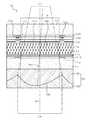
液晶装置10は、図3に示すように、ガラス、プラスチックなどの透明な一対の基板11,12をシール材13で所定間隔(例えば3〜10μm程度の間隔)を隔てて貼り合わせてなり、基板11と基板12の間のシール材13で囲まれた領域に液晶を密封して液晶層14を構成したものである。基板11の外面上及び基板12の外面上には偏光板15,16が配置されている。基板12には基板11の外形より外側に張り出す基板張出部12tが設けられ、この基板張出部12tの表面上に液晶ドライバ回路などが形成されてなる半導体装置17が実装されている。また、基板張出部12tの端部には、半導体装置17に導電接続された入力端子列が形成され、この入力端子列に導電接続するように、その端部にフレキシブル配線基板18が実装されている。
As shown in FIG. 3, the
図1に示すように、基板11の内面上には、画素領域Pの周縁部にCrなどの金属や黒色樹脂などで遮光膜11aが形成され、この上にSiO2などの無機絶縁体やアクリル樹脂などの合成樹脂で絶縁膜11bが形成され、この絶縁膜11b上にITO(インジウムスズ酸化物)などの透明導電体で対向電極11cが形成されている。対向電極11cの上にはSiO2等の斜方蒸着膜などからなる垂直膜向膜11dが形成されている。
As shown in FIG. 1, on the inner surface of the
基板12の内面上には、画素領域Pの周縁部に遮光膜12aが形成され、この上に無機絶縁体や合成樹脂で絶縁膜12bが形成され、この絶縁膜12b上に後述するTFT(薄膜トランジスタ)などからなるスイッチング素子12cが形成されている。このスイッチング素子12cは図示しない走査線に接続されている。また、スイッチング素子12c上には絶縁膜12dが形成され、この絶縁膜12d上には、上記スイッチング素子12cに導電接続されたデータ線12eが形成されている。なお、このデータ線12eは、上記走査線と直交する方向に伸びるように構成されている。データ線12e上にはさらに絶縁膜12fが形成され、この絶縁膜12f上に画素電極12gが透明導電体で形成されている。画素電極12g上には、上記と同様の斜方蒸着膜などからなる垂直配向膜12hが形成されている。
On the inner surface of the
本実施形態の液晶装置10はいわゆるVAモードの液晶装置であり、液晶層14は誘電異方性が負の液晶で構成され、例えばネガ型ネマチック液晶などで構成される。液晶層14内には多数の液晶分子14mが所定の配向状態となるように配置されている。具体的には、液晶層14は、対向電極11cと画素電極12gとの間に電界が印加されていないとき(電界無印加時)には、液晶分子14mが基板法線Nに対してほぼ平行に配向する(初期配向状態になる)垂直配向モードの液晶層となっている。また、対向電極11cと画素電極12gとの間に電界が印加されると、その電界強度に応じて液晶分子14mは所定の方位角に向けて倒れるように配向する。
The
基板11の外面上にはマイクロ光学素子アレイ19が形成されている。このマイクロ光学素子アレイ19は、基板11の外面上に形成された第1光学層19Aと、この第1光学層19A上に形成された第2光学層19Bを有する。第1光学層19A及び第2光学層19Bは材質の異なる光透過性の合成樹脂などで形成できる。図示例の場合、第1光学層19Aの光屈折率は第2光学層19Bの光屈折率よりも大きくされている。
A micro
マイクロ光学素子アレイ19は、第1光学層19Aと第2光学層19Bのうち、画素領域P毎に所定の光学機能を呈する光学素子部19Cが形成され、これらの複数の光学素子部19Cが画素領域Pの配列態様と整合した状態で配列されてなるものである。この光学素子部19Cは、光入射側(図示下側)から基板法線Nの方向に入射する光を集光する集光機能と、当該入射光の光軸Axを基板法線Nに対して傾斜させて、液晶層14に向ける光軸傾斜機能とを備えている。上記のように第1光学層19Aの光屈折率は第2光学層19Bの光屈折率よりも大きくなっているため、第1光学層19Aと第2光学層19Bの接合界面で構成される光学面が光入射側に凸の曲面状に形成されることにより、光学素子部19Cは集光機能を呈するものとなっている。また、上記の光学面は基板法線Nに対して非対称に構成され、これにより光学素子部19Cは光軸傾斜機能を呈するものとなっている。換言すれば、上記の第1光学層19Aは、凸レンズ状の集光素子として機能するとともに、プリズムのような光軸偏向素子(光屈折素子)として機能する。図示例では、画素領域P内の中央を通過する基板法線Nを対称軸とした場合、光学素子部19Cの光学面は図1の左右に非対称な面形状を有する。また、図示しないが、図1の紙面と直交する前後方向については光学素子部19Cの光学面は前後方向に対称な形状を有する。
The micro
図1に示す液晶層14内にある液晶分子14mは、図2(a)に実線で示すように、初期配向状態において、その長軸方向を基板法線Nの方向にほぼ平行にした姿勢に配向される。ただし、液晶分子14mの長軸方向は基板法線Nに対して完全に平行ではなく、僅かな角度差θtを有している。液晶分子14mのプレチルト角θpは90−θt、すなわち90度未満である。プレチルト角θpは、通常、85〜90度の範囲内に設定され、特に、87〜89度の範囲内であることが好ましい。
The
上記のプレチルト角θpは液晶分子14mの種類、液晶層14の厚さ(セルギャップ)、垂直配向膜11d、12hの種類や構造などによって異なる。例えば、本実施形態では、垂直配向膜11d,12hとして、共に基板11,12の表面に対して約50度の角度でSiO2を蒸着してなる斜方蒸着膜を用い、プレチルト角θpを88度としている。また、図2(b)に示すように、基板法線Nの方向から見たとき、液晶分子14mは方位角θdで表される方位に向けてプレチルト角θpにて傾斜している。
The pretilt angle θp varies depending on the type of
本実施形態において、液晶分子14mのプレチルトの方位角θdは液晶層14全体に亘って揃えてある。図1では、プレチルトの方位角θdは全て図示右側に設定されている。このような構成は、斜方蒸着膜で垂直配向膜11d、12hを構成する場合には、斜方蒸着膜の蒸着方位によって決定されるので、きわめて簡単に製造できる。
In the present embodiment, the azimuth angle θd of the pretilt of the
上記のように設定された、液晶分子14mのプレチルトの方位角θdにより、対向電極11cと画素電極12gとの間に所定の電圧を印加したとき、液晶分子14mは上記方位角θdの方位に向けて倒れるように配向する。これによって、液晶分子14mの電界印加時における配向方位を制御することができ、不所望な光学特性が現れることを防止できる。
When a predetermined voltage is applied between the
上記の光学素子部19Cの光軸傾斜機能は、基板法線Nの方向から入射した光の光軸Axを、液晶層14の内部において基板法線Nに対して上記液晶分子14mのプレチルトの方位角の側に傾斜させるように作用する。すなわち、図1において上記方位角が図示右側を向いている場合には、光軸Axを図示右側に傾斜させる。このとき、光軸Axの傾斜角が上記のプレチルト角θpとほぼ一致するように構成されること、すなわち、光軸Axと初期配向状態における液晶分子14mの長軸方向とが平行になるように構成されることが望ましい。
The optical axis tilting function of the
上記の光学素子部19Cは、液晶層14の光入射側において光学的に作用する。このとき、光軸Axは、マイクロ光学素子アレイ19と基板12との界面、基板12と液晶層14との界面、その他の界面において種々に屈折するため、最終的に液晶層14の内部に光が入射したときに、光軸Axがプレチルトの方位角側に傾斜するように構成されていればよい。したがって、光軸偏向手段は、基板12の外面上でなくても、基板12の外側に離反して配置されていてもよく、或いは、基板12の内面形状によって形成されていてもよく、さらには、基板12の内面上に形成されていても構わない。
The
図4は、上記実施形態の各画素領域Pにそれぞれ設けられるスイッチング素子12cのより詳細な構造を示す拡大断面図である。基板12上には上述のように遮光膜12a及び絶縁膜12bが形成され、この絶縁膜12b上の遮光膜12aによって遮光される領域に、シリコン薄膜などで構成される半導体層12caが形成される。半導体層12caは、ゲート絶縁膜12cbによって覆われ、このゲート絶縁膜12cb上における半導体層12caの活性領域(チャネル領域)に対向する位置にゲート電極12cgが形成される。このゲート電極12cgは、図示しない走査線に導電接続されている。
FIG. 4 is an enlarged cross-sectional view showing a more detailed structure of the switching
また、半導体層12caのソース領域には絶縁膜12dに形成されたコンタクトホールを介してデータ線12eが導電接続され、半導体層12caのドレイン領域には絶縁膜12d及び12fに形成されたコンタクトホールを介して画素電極12gが導電接続されている。さらに、半導体層12caに対しては上記ゲート絶縁膜12cbを介して容量線12ccの一部が対向配置されている。
Further, the
図5(a)乃至(c)は、本実施形態におけるマイクロ光学素子アレイ19の製造工程を示す工程説明図である。本実施形態では、図5(a)に示すように、基板12の外面上に未硬化のアクリル樹脂などからなる基材19aをスピンコーティング法などにより塗布し、これを型1で成形し、所定の硬化処理(たとえば、基材19aが光(紫外線)硬化樹脂であれば光(紫外線)照射処理、基材19aが熱効果樹脂であれば加熱処理、基材19aが熱可塑性樹脂であれば冷却若しくは乾燥処理など)で硬化させることにより、図5(b)に示すように第1光学層19Aを形成する。そして、第1光学層19Aの上にさらにスピンコーティング法などにより未硬化の基材を表面が平坦となるように塗布し、これを硬化させて第2光学層19Bを形成する。
FIGS. 5A to 5C are process explanatory views showing the manufacturing process of the micro
なお、本実施形態におけるマイクロ光学素子アレイ19の製造方法としては、上記方法に限らず、ガラスや透明樹脂などの光学層の表面上に所定のマスクをフォトリソグラフィ法などによって形成し、その表面に等方性エッチングを施すことなどによって上記の光学素子部19Cを構成する光学面を形成してもよい。この場合、基板12上において上記の処理を実施してもよく、或いは、上記の処理をして光学フィルムを形成し、この光学フィルムを基板12に貼着するようにしても構わない。
In addition, the manufacturing method of the micro
本実施形態では、図1に示すように、基板法線Nの方向に入射光束Laが入射すると、光学素子部19Cによって集光されるとともに、その光軸Axが基板法線Nに対して傾斜し、この傾斜方向が液晶分子14mのプレチルトの方位角に一致するので、液晶層14に入射する光の進行方向が液晶分子14mの長軸方向に傾斜し、その結果、上記進行方向と上記長軸方向の角度差が低減されることから、初期配向状態における液晶層14による入射光へのリタデーションが小さくなる。したがって、偏光板15及び16の偏光透過軸を一致させ、初期配向状態において光透過状態が実現されるように構成される場合には、液晶装置10の光透過率を高めることができる。また、偏光板15及び16の偏光透過軸を相互に直交させ、初期配向状態において光遮断状態が実現されるように構成される場合には、液晶装置10の光漏れを低減することができる。特に、上述のように、初期配向状態において、光軸Axと液晶分子14mの長軸方向とが平行になるように構成することにより、上記の光透過率の低下や光漏れを大幅に低減できる。
In the present embodiment, as shown in FIG. 1, when an incident light beam La enters in the direction of the substrate normal N, it is condensed by the
なお、出射光束Lbは、基板法線Nの方向に対して光軸Axが僅かに傾斜していることから、やや斜めに出射されることになるが、このままで支障がなければ図示の構成で良く、出射光束Lbの光軸を再び基板法線Nの方向に修正する必要があれば、基板11上に別途設けた光軸復元手段を用いて復元することができる。また、この光軸復元手段は、液晶装置とは別途に設けられた光学系によって実現してもよい。
The emitted light beam Lb is emitted slightly obliquely because the optical axis Ax is slightly inclined with respect to the direction of the substrate normal N. However, if there is no problem in this state, the configuration shown in the drawing is used. If it is necessary to correct the optical axis of the emitted light beam Lb again in the direction of the substrate normal N, it can be restored by using an optical axis restoring means separately provided on the
また、本実施形態では、光軸偏向手段を構成する光学素子部19Cが光入射側の基板12に対して一体に形成されていることにより、液晶層14の入射側において光軸Axを確実に傾斜させることができるとともに、基板12との一体化により製造時の取扱が容易になる。また、光学素子部19Cは基板12の外面上に形成されているので、液晶層14に対する電界印加に影響を与えることもない。
In the present embodiment, the
さらに、本実施形態では、光学素子部19Cが集光機能をも有するので、画素領域P内に入射光を効率的に導入することができ、液晶装置10の開口率を実質的に向上させることができる。また、この集光機能は光軸偏向手段を構成する光学素子部19Cによって確保されるため、集光レンズ部を別途形成する必要がなくなり、その結果、光学素子部19Cの薄肉化や製造工程の簡略化を図ることができる。
Furthermore, in this embodiment, since the
[第2実施形態]
次に、図6を参照して本発明に係る第2実施形態について説明する。この実施形態は、上記第1実施形態と共通の基本構造を有するので、同一部分には同一符号を付し、それらの説明は省略する。この実施形態は、基板12の外面上に形成されたマイクロ光学素子アレイ19′の構造のみが第1実施形態と異なるため、以下、マイクロ光学素子アレイ19′の構造について説明する。
[Second Embodiment]
Next, a second embodiment according to the present invention will be described with reference to FIG. Since this embodiment has the same basic structure as the first embodiment, the same reference numerals are given to the same parts, and the description thereof is omitted. Since this embodiment is different from the first embodiment only in the structure of the micro
図6に示すように、マイクロ光学素子アレイ19′は、基板12の外面上に第1光学層19D、第2光学層19E及び第3光学層19Fが積層されてなり、画素領域P毎に、第1光学素子部19Gと、第2光学素子部19Hとが基板法線Nの方向に積層された構造を有する。ここで、第1光学層19Dの光屈折率>第2光学層19Eの光屈折率>第3光学層19Fの光屈折率となるように構成される。上記第1光学層19Dはプリズム状の光軸偏向素子(光屈折素子)を構成する。また、上記第2光学層19Eは凸レンズ状の集光素子を構成する。
As shown in FIG. 6, the micro
第1光学素子部19Gは、第2光学層19Eと第3光学層19Fとの接合界面からなる光学面により構成され、当該光学面が基板法線Nと平行な光学中心軸を備えた集光レンズ機能を備えている。第2光学素子部19Hは、第1光学層19Dと第2光学層19Eとの接合界面からなる光学面により構成され、当該光学面が基板法線Nと直交する平面に対して傾斜していることにより、入射光束Laの光軸を基板法線Nに対して所定角度傾斜させる機能を備えている。
The first
図7(a)乃至(e)は、本実施形態のマイクロ光学素子アレイ19′の製造工程を示す工程説明図である。この実施形態では、図7(a)に示すように、基板12の外面上に未硬化の樹脂等の基材19dをスピンコーティング法などにより塗布した後、図7(b)に示すように、型2を用いて基材19を成形し、第1実施形態と同様に所定の処理によって硬化させ、第1光学層19Dを形成する。次に、図7(c)に示すように、第1光学層19Dの上に未硬化樹脂からなる基材19eを塗布し、その後、図7(d)に示すように、型3を用いて基材19eを成形し、これを硬化させることにより第2光学層19Eを形成する。最後に、図7(e)に示すように、第2光学層19Eの上に未硬化の樹脂からなる基材を表面が平坦になるように塗布し、これを硬化させることにより、第3光学層19Fを形成する。
FIGS. 7A to 7E are process explanatory views showing the manufacturing process of the micro
本実施形態では、第1実施形態の効果に加えて、集光機能を有する第1光学素子部(集光レンズ)19Gと、光軸偏向手段として光軸傾斜機能を発揮する第2光学素子部19Hとが別々に構成されていることにより、それぞれの構造(図示の場合には各光学素子を構成する光学面)を簡易かつ高精度に形成することができる。すなわち、第1実施形態においては、上記光学素子部19Cを構成する光学面を基板法線Nに対して非対称で、しかも、集光機能を有する曲面形状とする必要があり、複雑な曲面形状を形成しなければならないが、本実施形態では、集光機能を有する第1光学素子部19Gの光学面と、光軸傾斜機能を有する第2光学素子部19Hの光学面とが基板法線Nの方向に別々に配置されているため、製造工数は増えるものの、それぞれの製造工程の歩留まりや光学面精度の向上を図ることが可能になる。
In the present embodiment, in addition to the effects of the first embodiment, a first optical element section (condensing lens) 19G having a condensing function and a second optical element section that exhibits an optical axis tilt function as an optical axis deflecting unit By being configured separately from 19H, each structure (in the illustrated case, an optical surface constituting each optical element) can be formed easily and with high accuracy. That is, in the first embodiment, it is necessary that the optical surface constituting the
[第3実施形態]
次に、図8を参照して本発明に係る電子機器の構成例を第3実施形態として説明する。図8は、液晶装置を光変調手段として備えた投射型表示装置の構成例を示すものである。この投射型表示装置100は、光源120と、色分離合成系140と、投射光学系160とから構成されている。ここで、後述するように、R(Red:赤)、G(Green:緑)、B(blue:青)の異なる色光毎に本発明に係る液晶装置を構成する透過型液晶ライトバルブを光変調手段として備えている。
[Third Embodiment]
Next, a configuration example of an electronic apparatus according to the invention will be described as a third embodiment with reference to FIG. FIG. 8 shows an example of the configuration of a projection display device provided with a liquid crystal device as a light modulation means. The
光源120は、高圧水銀ランプ或いはメタルハライドランプ等のランプ121と、ランプ121の光を反射するリフレクタ122と、ランプ121の光の照度分布を均一化させるための2枚のフライアイレンズ123、124と、光の偏光方向を一方向に揃える偏光変換板126を有する。
The
ここで、2枚のフライアイレンズ123、124は、それぞれ例えば6×8個のような複数のレンズ123a、124aを縦横に配列したものであり、ランプ121の光Lが2枚のフライアイレンズ123、124を順次透過することによって、光Lの照度分布を均一化させるようになっている。
Here, the two fly-
偏光変換板126は、2枚のフライアイレンズ側に設けられた図示しない偏光ビームスプリッタアレイ(PBSアレイ)と、PBSアレイによって反射された偏光の偏光方向を変換する図示しない1/2波長板アレイとから構成され、ランプ121の光Lはその輝度を損なうことなく光の偏光方向を一方向に揃えるようになっている。
The
また、色分離合成系140は、ダイクロイックミラー141、142と、反射ミラー143、144、145と、リレーレンズ146、147、148と、液晶ライトバルブ151、152、153と、クロスダイクロイックプリズム155とを有する。
The color separation /
ダイクロイックミラー141、142は、例えばガラス表面に誘電体多層膜を積層したもので、所定の有色光を選択的に反射し、それ以外の波長の光を透過するようになっている。具体的には、ダイクロイックミラー141は、光源120の光Lのうち、赤色光LRを透過させるとともに、青色光LB及び緑色光LGを反射するようになっている。また、ダイクロイックミラー142はダイクロイックミラー141で反射された青色光LB及び緑色光LGのうち、青色光LBを透過させるとともに、緑色光LGを反射するようになっている。
The dichroic mirrors 141 and 142 are formed by, for example, laminating a dielectric multilayer film on the glass surface, and selectively reflect predetermined colored light and transmit light of other wavelengths. Specifically, the
これにより、光源120から入射した光のうち、赤色光LRはダイクロイックミラー141を透過した後、反射ミラー145で反射され、赤色光用の液晶ライトバルブ151に入射される。緑色光LGはダイクロイックミラー141に反射されて緑色光用の液晶ライトバルブ152に入射される。青色光LBはダイクロイックミラー142を透過した後、リレーレンズ146、反射ミラー143、リレーレンズ147、反射ミラー144、及び、リレーレンズ148からなるリレー系140aを経て、青色光用の液晶ライトバルブ153に入射されるようになっている。
As a result, the red light LR out of the light incident from the
液晶ライトバルブ151、152、153は、例えばアクティブマトリクス型の透過型液晶ライトバルブとして構成されており、信号処理された画像信号に基づいて駆動回路により駆動されるようになっている。そして、各液晶ライトバルブ151、152、153によって変調された有色光は、クロスダイクロイックプリズム155に入射されるようになっている。
The liquid crystal
クロスダイクロイックプリズム155は、直角プリズムが貼り合わされた構造となっており、その内面に赤色光LRを反射するミラー面と青色光LBを反射するミラー面とが十字状に形成されている。したがって、クロスダイクロイックプリズム155は3つの色光LR、LG、LBをこれらのミラー面によって合成して、カラー画像を表示する合成光を形成するようになっている。
The cross
また、投射光学系160は投射レンズ161、162、163とスクリーン165とを有する。投射レンズ161、162、163はクロスダイクロイックプリズム155によって形成された合成光をスクリーン165の上に拡大投射するようになっている。これによって、スクリーン165にカラー画像が表示される。
The projection
本実施形態において、液晶ライトバルブ151,152,153は、それぞれ第1実施形態若しくは第2実施形態に記載の液晶装置10,10′によって構成することができる。これによって、上記光軸偏向手段により光透過率の向上或いは光漏れの低減を図ることができるとともに、集光機能による明るさの増大を図ることができる。
In the present embodiment, the liquid crystal
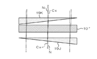
なお、本実施形態の液晶ライトバルブ151,152,153としては、図9に示す液晶装置10″を用いることも可能である。この場合、この液晶装置10″は、上記液晶装置10,10′の構成のうち、マイクロ光学素子アレイ19,19′を除去した(或いは、光軸偏向手段のみを除去し、集光レンズが残された)構造を備えている。また、液晶装置10″の液晶層は、全体において液晶分子のプレチルトの方位角が揃うように構成されている。この場合には、液晶装置10″に光軸偏向手段を設けるのではなく、投射型表示装置100内における光学系と、液晶装置10″との位置関係によって光軸偏向手段が構成されている。すなわち、液晶装置10″は、図8に示す色分離合成系140によって構成される光路の光軸Bxに対して、その基板法線Nの方向を所定角度傾けた姿勢で固定されている。そして、その結果、液晶装置10″の液晶層の内部にて光軸Bxが基板法線Nに対して液晶分子のプレチルトの方位角側に傾斜するようにしている。この場合においても、液晶層内において光軸Bxの傾きが液晶分子のプレチルト角に対応する角度に設定され、光軸Bxと液晶分子の長軸方向とが液晶層内においてほぼ平行に構成されることが好ましい。
Note that the
図10は、本実施形態の別の構成例を示す概略構成図である。この構成例では、投射型表示装置100の内部において、上記の液晶ライトバルブ151,152,153として構成された液晶装置10″の光入射側に光軸偏向手段であるプリズム状の光軸偏向素子(光屈折素子)19Jを配置している。この光軸偏向素子19Jは上記光路の光軸Cxを偏向させ、この偏向した光軸を有する光が液晶装置10″に入射されることにより、上記と同様に、液晶層内において光軸Cxが基板法線に対して液晶分子のプレチルトの方位角の側に傾斜するように構成されている。特に、液晶層内において基板法線に対して光軸Cxがプレチルト角に相当する角度だけ傾斜し、その結果、当該光軸Cxと、液晶分子の長軸とが平行になるように構成されていることが好ましい。
FIG. 10 is a schematic configuration diagram showing another configuration example of the present embodiment. In this configuration example, a prism-shaped optical axis deflecting element serving as an optical axis deflecting means is provided on the light incident side of the
また、この液晶装置10″の光出射側には、上記のように偏向された光軸Cxを元に戻すための光軸偏向手段であるプリズム状の光軸偏向素子19Kが配置されている。この光軸偏向素子19Kは、液晶装置10″の基板法線Nに対して上述のように傾斜した光軸Cxを基板法線Nに対して平行になるように偏向させ、その結果、液晶装置10″から出射する光の光軸Cxが、光軸偏向素子19Jに入射する前の光軸と一致する(或いは平行になる)ように構成されている。これによって、光出射側の光学系を特に調整することなく、従来と同様の構成で投射型表示装置を構成することが可能になる。
Further, a prism-shaped optical
投射型表示装置を構成するためには、明るく、コントラストの高い表示態様が要求されるが、本実施形態では、光変調手段として設けられた液晶装置において、光軸偏向手段により、液晶層の内部における光軸が基板法線に対して液晶分子のプレチルトの方位角の側に傾斜することにより、光透過率の向上や光漏れの低減を図ることができるため、上記要求を容易に満たすことが可能になる。 In order to configure a projection display device, a bright and high-contrast display mode is required. In this embodiment, in the liquid crystal device provided as the light modulation unit, the inside of the liquid crystal layer is formed by the optical axis deflection unit. By tilting the optical axis at the side of the pretilt azimuth angle of the liquid crystal molecules with respect to the substrate normal, it is possible to improve light transmittance and reduce light leakage, so that the above requirements can be easily satisfied. It becomes possible.
[第4実施形態]
図11は、本実施形態の電子機器における液晶装置10に対する制御系(表示制御系)の全体構成を示す概略構成図である。ここに示す電子機器は、表示情報出力源291と、表示情報処理回路292と、電源回路293と、タイミングジェネレータ294とを含む表示制御回路290を有する。また、液晶装置10には、上述の構成を有するパネル構造10Pと、このパネル構造10Pを駆動する駆動回路10Dとが設けられている。この駆動回路10Dは、パネル構造10Pに直接実装されている電子部品(半導体ICなど)で構成される。ただし、駆動回路10Dは、上記のような態様の他に、パネル構造10Pの基板表面上に形成された回路パターン、或いは、パネル構造10Pに導電接続された回路基板に実装された半導体ICチップ若しくは回路パターンなどによっても構成することができる。
[Fourth Embodiment]
FIG. 11 is a schematic configuration diagram illustrating an overall configuration of a control system (display control system) for the
表示情報出力源291は、ROM(Read Only Memory)やRAM(Random Access Memory)等からなるメモリと、磁気記録ディスクや光記録ディスク等からなるストレージユニットと、デジタル画像信号を同調出力する同調回路とを備え、タイミングジェネレータ294によって生成された各種のクロック信号に基づいて、所定フォーマットの画像信号等の形で表示情報を表示情報処理回路292に供給するように構成されている。
The display
表示情報処理回路292は、シリアル−パラレル変換回路、増幅・反転回路、ローテーション回路、ガンマ補正回路、クランプ回路等の周知の各種回路を備え、入力した表示情報の処理を実行して、その画像情報をクロック信号CLKと共に駆動回路10Dへ供給する。駆動回路10Dは、走査線駆動回路、信号線駆動回路及び検査回路を含む。また、電源回路293は、上述の各構成要素にそれぞれ所定の電圧を供給する。
The display
図12は、本発明に係る電子機器の一実施形態である携帯電話の外観を示す。この電子機器1000は、操作部1001と、表示部1002とを有し、表示部1002の筐体内部に回路基板1003が配置されている。回路基板1003上には上記の液晶装置10が実装されている。そして、表示部1002の表面において上記パネル構造10Pの表示領域を視認できるように構成されている。この場合、液晶装置10の背後には図示しないバックライトが配置され、このバックライトからの光の光軸が上記光軸偏向手段によって偏向されるように構成される。
FIG. 12 shows the appearance of a mobile phone which is an embodiment of the electronic apparatus according to the present invention. The
本発明は、上述した実施形態に限られるものではなく、請求の範囲及び明細書全体から読み取れる発明の要旨、あるいは思想に反しない範囲で適宜変更可能であり、そのような変更を伴う液晶装置もまた、本発明の技術的範囲に含まれるものである。例えば、上記実施形態ではTFTやTFDなどのスイッチング素子を備えたアクティブマトリクス型の液晶表示装置を想定して説明したが、本発明は、スイッチング素子を持たない装置構成、例えば、パッシブマトリクス型の装置構成に適用することも可能である。 The present invention is not limited to the above-described embodiments, and various modifications can be made as appropriate without departing from the spirit or concept of the invention that can be read from the claims and the entire specification. Moreover, it is included in the technical scope of the present invention. For example, in the above embodiment, the active matrix type liquid crystal display device provided with switching elements such as TFT and TFD has been described. However, the present invention is a device configuration having no switching elements, for example, a passive matrix type device. It is also possible to apply to the configuration.
また、上記第1及び第2実施形態の光軸偏向手段は、集光機能をも有する光学素子で構成されているが、光学素子部に集光機能を持たせず、光軸偏向機能のみが実現されるように構成してもよい。 The optical axis deflecting means of the first and second embodiments is composed of an optical element having a condensing function. However, the optical element portion does not have a condensing function and only the optical axis deflecting function is provided. You may comprise so that it may be implement | achieved.
10…液晶装置、11,12…基板、11c…対向電極、12c…スイッチング素子、12g…画素電極、11d,12h…垂直配向膜、14…液晶層、14m…液晶分子、θp…プレチルト角、19,19′…マイクロ光学素子アレイ、19A…第1光学層、19B…第2光学層、19C…光学素子部、19D…第1光学層、19E…第2光学層、19F…第3光学層、19G…第1光学素子部(集光レンズ)、19H…第2光学素子部(光軸偏向素子)、100…電子機器(投射型表示装置)、290…表示制御回路、1000…電子機器(携帯電話)
DESCRIPTION OF
Claims (12)
前記初期配向状態において前記液晶分子が90度未満のプレチルト角を有し、かつ、少なくとも前記基板面内の所定範囲内において前記液晶分子のプレチルトの方位角が実質的に揃うように構成され、
少なくとも前記基板面内の前記所定範囲内において前記基板法線方向から入射する光の光軸を前記液晶分子の前記プレチルト角の前記方位角側に傾斜させる光軸偏向手段を具備することを特徴とする液晶装置。 A pair of substrates, a liquid crystal layer disposed between the pair of substrates, and an electric field application structure for applying an electric field to the liquid crystal layer, wherein the liquid crystal molecules in the liquid crystal layer are substantially free when no electric field is applied. In a liquid crystal device having an initial alignment state aligned in the substrate normal direction,
In the initial alignment state, the liquid crystal molecules have a pretilt angle of less than 90 degrees, and at least within a predetermined range in the substrate surface, the azimuth angles of the liquid crystal molecules are substantially aligned.
Characterized in that it comprises optical axis deflecting means for tilting the optical axis of light incident from the normal direction of the substrate within the predetermined range within the substrate plane toward the azimuth side of the pretilt angle of the liquid crystal molecules. Liquid crystal device.
前記光軸偏向手段は、前記光学素子部の基板法線に対する非対称構造により実現されていることを特徴とする請求項1乃至4のいずれか一項に記載の液晶装置。 A plurality of pixels configured to be able to apply an electric field substantially independently; and a micro optical element array disposed on the incident side with respect to the liquid crystal layer and having an optical element portion for each pixel;
5. The liquid crystal device according to claim 1, wherein the optical axis deflecting unit is realized by an asymmetric structure with respect to a substrate normal line of the optical element unit.
前記液晶装置に光を照射する光源と、
を具備し、
前記液晶装置では、前記初期配向状態において前記液晶分子が90度未満のプレチルト角を有し、かつ、少なくとも前記基板面内の所定範囲内において前記液晶分子のプレチルトの方位角が実質的に揃うように構成され、
少なくとも前記基板面内の前記所定範囲内において前記基板法線方向に対して前記光源から入射する光の光軸が前記液晶装置における前記液晶分子の前記プレチルト角の前記方位角側に傾斜している
ことを特徴とする電子機器。 A pair of substrates, a liquid crystal layer disposed between the pair of substrates, and an electric field application structure for applying an electric field to the liquid crystal layer, wherein the liquid crystal molecules in the liquid crystal layer are substantially free when no electric field is applied. A liquid crystal device having an initial alignment state aligned in the substrate normal direction;
A light source for irradiating the liquid crystal device with light;
Comprising
In the liquid crystal device, the liquid crystal molecules have a pretilt angle of less than 90 degrees in the initial alignment state, and the pretilt azimuth angles of the liquid crystal molecules are substantially aligned at least within a predetermined range in the substrate surface. Composed of
The optical axis of light incident from the light source with respect to the normal direction of the substrate is tilted toward the azimuth side of the pretilt angle of the liquid crystal molecules in the liquid crystal device at least within the predetermined range in the substrate surface. An electronic device characterized by that.
The electronic apparatus according to claim 8, wherein the electronic apparatus is a projection display device having a light projection unit that projects an image light-modulated by the liquid crystal device.
Priority Applications (1)
| Application Number | Priority Date | Filing Date | Title |
|---|---|---|---|
| JP2004379206A JP2006184673A (en) | 2004-12-28 | 2004-12-28 | Liquid crystal device and electronic apparatus |
Applications Claiming Priority (1)
| Application Number | Priority Date | Filing Date | Title |
|---|---|---|---|
| JP2004379206A JP2006184673A (en) | 2004-12-28 | 2004-12-28 | Liquid crystal device and electronic apparatus |
Publications (2)
| Publication Number | Publication Date |
|---|---|
| JP2006184673A true JP2006184673A (en) | 2006-07-13 |
| JP2006184673A5 JP2006184673A5 (en) | 2007-03-08 |
Family
ID=36737823
Family Applications (1)
| Application Number | Title | Priority Date | Filing Date |
|---|---|---|---|
| JP2004379206A Withdrawn JP2006184673A (en) | 2004-12-28 | 2004-12-28 | Liquid crystal device and electronic apparatus |
Country Status (1)
| Country | Link |
|---|---|
| JP (1) | JP2006184673A (en) |
Cited By (13)
| Publication number | Priority date | Publication date | Assignee | Title |
|---|---|---|---|---|
| EP1967870A1 (en) * | 2007-03-06 | 2008-09-10 | Rohm and Haas Denmark Finance A/S | Display comprising a light redirecting film having variable thickness |
| WO2008155878A1 (en) * | 2007-06-18 | 2008-12-24 | Sharp Kabushiki Kaisha | Liquid crystal display device |
| US7995887B2 (en) | 2005-08-03 | 2011-08-09 | Sharp Kabushiki Kaisha | Liquid crystal display device and electronic device using the same |
| US7995167B2 (en) | 2006-10-18 | 2011-08-09 | Sharp Kabushiki Kaisha | Liquid crystal display device and method for manufacturing liquid crystal display device |
| US8111356B2 (en) | 2006-09-12 | 2012-02-07 | Sharp Kabushiki Kaisha | Liquid crystal display panel provided with microlens array, method for manufacturing the liquid crystal display panel, and liquid crystal display device |
| US8243236B2 (en) | 2006-10-18 | 2012-08-14 | Sharp Kabushiki Kaisha | Liquid crystal display and method for manufacturing liquid crystal display |
| US8289461B2 (en) | 2007-01-24 | 2012-10-16 | Sharp Kabushiki Kaisha | Liquid crystal display device |
| US8384860B2 (en) | 2007-06-26 | 2013-02-26 | Sharp Kabushiki Kaisha | Liquid crystal display device and method of manufacturing liquid crystal display device |
| US8403546B2 (en) | 2009-09-30 | 2013-03-26 | Denso Corporation | Illuminating device |
| US8421967B2 (en) | 2006-12-14 | 2013-04-16 | Sharp Kabushiki Kaisha | Liquid crystal display device and process for producing liquid crystal display device |
| US8659726B2 (en) | 2007-04-13 | 2014-02-25 | Sharp Kabushiki Kaisha | Liquid crystal display and method of manufacturing liquid crystal display |
| JP2016024205A (en) * | 2014-07-16 | 2016-02-08 | セイコーエプソン株式会社 | Micro lens array substrate, electro-optic device, and electronic apparatus |
| US9551896B2 (en) | 2013-02-05 | 2017-01-24 | Seiko Epson Corporation | Liquid crystal device and electronic apparatus including a plurality of microlenses separated by a liquid crystal layer |
Families Citing this family (3)
| Publication number | Priority date | Publication date | Assignee | Title |
|---|---|---|---|---|
| CN101395525B (en) | 2006-03-23 | 2010-11-10 | 夏普株式会社 | Liquid crystal display device |
| WO2008038487A1 (en) | 2006-09-28 | 2008-04-03 | Sharp Kabushiki Kaisha | Liquid crystal display panel with microlens array, its manufacturing method, and liquid crystal display device |
| WO2008084589A1 (en) | 2007-01-11 | 2008-07-17 | Sharp Kabushiki Kaisha | Liquid crystal display panel with micro-lens array and liquid crystal display device |
Citations (4)
| Publication number | Priority date | Publication date | Assignee | Title |
|---|---|---|---|---|
| JPS6242182A (en) * | 1985-08-20 | 1987-02-24 | 株式会社精工舎 | Projection type liquid crystal display unit |
| JPH0519303A (en) * | 1991-07-09 | 1993-01-29 | Toshiba Corp | Projection type liquid crystal display device |
| JPH05232461A (en) * | 1992-02-19 | 1993-09-10 | Sanyo Electric Co Ltd | Liquid crystal panel |
| JPH09245370A (en) * | 1996-03-12 | 1997-09-19 | Pioneer Electron Corp | Optical pickup |
-
2004
- 2004-12-28 JP JP2004379206A patent/JP2006184673A/en not_active Withdrawn
Patent Citations (4)
| Publication number | Priority date | Publication date | Assignee | Title |
|---|---|---|---|---|
| JPS6242182A (en) * | 1985-08-20 | 1987-02-24 | 株式会社精工舎 | Projection type liquid crystal display unit |
| JPH0519303A (en) * | 1991-07-09 | 1993-01-29 | Toshiba Corp | Projection type liquid crystal display device |
| JPH05232461A (en) * | 1992-02-19 | 1993-09-10 | Sanyo Electric Co Ltd | Liquid crystal panel |
| JPH09245370A (en) * | 1996-03-12 | 1997-09-19 | Pioneer Electron Corp | Optical pickup |
Cited By (14)
| Publication number | Priority date | Publication date | Assignee | Title |
|---|---|---|---|---|
| US7995887B2 (en) | 2005-08-03 | 2011-08-09 | Sharp Kabushiki Kaisha | Liquid crystal display device and electronic device using the same |
| US8111356B2 (en) | 2006-09-12 | 2012-02-07 | Sharp Kabushiki Kaisha | Liquid crystal display panel provided with microlens array, method for manufacturing the liquid crystal display panel, and liquid crystal display device |
| US8243236B2 (en) | 2006-10-18 | 2012-08-14 | Sharp Kabushiki Kaisha | Liquid crystal display and method for manufacturing liquid crystal display |
| US7995167B2 (en) | 2006-10-18 | 2011-08-09 | Sharp Kabushiki Kaisha | Liquid crystal display device and method for manufacturing liquid crystal display device |
| US8421967B2 (en) | 2006-12-14 | 2013-04-16 | Sharp Kabushiki Kaisha | Liquid crystal display device and process for producing liquid crystal display device |
| US8289461B2 (en) | 2007-01-24 | 2012-10-16 | Sharp Kabushiki Kaisha | Liquid crystal display device |
| EP1967870A1 (en) * | 2007-03-06 | 2008-09-10 | Rohm and Haas Denmark Finance A/S | Display comprising a light redirecting film having variable thickness |
| US8659726B2 (en) | 2007-04-13 | 2014-02-25 | Sharp Kabushiki Kaisha | Liquid crystal display and method of manufacturing liquid crystal display |
| JPWO2008155878A1 (en) * | 2007-06-18 | 2010-08-26 | シャープ株式会社 | Liquid crystal display |
| WO2008155878A1 (en) * | 2007-06-18 | 2008-12-24 | Sharp Kabushiki Kaisha | Liquid crystal display device |
| US8384860B2 (en) | 2007-06-26 | 2013-02-26 | Sharp Kabushiki Kaisha | Liquid crystal display device and method of manufacturing liquid crystal display device |
| US8403546B2 (en) | 2009-09-30 | 2013-03-26 | Denso Corporation | Illuminating device |
| US9551896B2 (en) | 2013-02-05 | 2017-01-24 | Seiko Epson Corporation | Liquid crystal device and electronic apparatus including a plurality of microlenses separated by a liquid crystal layer |
| JP2016024205A (en) * | 2014-07-16 | 2016-02-08 | セイコーエプソン株式会社 | Micro lens array substrate, electro-optic device, and electronic apparatus |
Similar Documents
| Publication | Publication Date | Title |
|---|---|---|
| JP4923758B2 (en) | Liquid crystal display | |
| JP3708112B2 (en) | Manufacturing method and display device of display panel with microlens array | |
| JP6123317B2 (en) | Liquid crystal device and electronic device | |
| US7477348B2 (en) | Retarder, liquid crystal display element, and liquid crystal projector | |
| JP6337604B2 (en) | Electro-optical device manufacturing method, electro-optical device, and electronic apparatus | |
| JP2006184673A (en) | Liquid crystal device and electronic apparatus | |
| JP6384092B2 (en) | Liquid crystal device and electronic device | |
| US20080100759A1 (en) | Projector, optical compensation method therefor, and liquid crystal device | |
| JP2016151735A (en) | Lens array substrate, electro-optic device, electronic apparatus, and method for manufacturing lens array substrate | |
| KR100686498B1 (en) | Electro-optical device and method for fabricating the same, and projection display device | |
| JP4506183B2 (en) | Liquid crystal device and projection display device | |
| JP2009037025A (en) | Projector and liquid crystal device | |
| JP4315084B2 (en) | Microlens array plate and manufacturing method thereof, and electro-optical device and electronic apparatus including the same | |
| JP2022038106A (en) | Electro-optical device and electronic device | |
| JP4333373B2 (en) | Microlens manufacturing method, microlens, and electro-optical device and electronic apparatus including the same | |
| JP2021076734A (en) | Liquid crystal device and electronic apparatus | |
| US20090015733A1 (en) | Retardation Film and Projection Display Apparatus | |
| JP6299493B2 (en) | Microlens array substrate, electro-optical device, and electronic device | |
| JP6874818B1 (en) | Liquid crystal devices and electronic devices | |
| JP2012088418A (en) | Liquid crystal device, projection type display device and method for manufacturing liquid crystal device | |
| JP4639785B2 (en) | Phase difference plate, liquid crystal panel, projection type liquid crystal display device | |
| US20220066261A1 (en) | Display element and projection type display apparatus | |
| JP2021124623A (en) | Electro-optical device and electronic apparatus | |
| JP2021099395A (en) | Liquid crystal device and electronic apparatus | |
| JP2005266820A (en) | Exposure apparatus and method for forming microlens array by using the same |
Legal Events
| Date | Code | Title | Description |
|---|---|---|---|
| A521 | Written amendment |
Free format text: JAPANESE INTERMEDIATE CODE: A523 Effective date: 20070118 |
|
| A621 | Written request for application examination |
Free format text: JAPANESE INTERMEDIATE CODE: A621 Effective date: 20070118 |
|
| RD04 | Notification of resignation of power of attorney |
Free format text: JAPANESE INTERMEDIATE CODE: A7424 Effective date: 20070404 |
|
| A977 | Report on retrieval |
Free format text: JAPANESE INTERMEDIATE CODE: A971007 Effective date: 20100318 |
|
| A131 | Notification of reasons for refusal |
Free format text: JAPANESE INTERMEDIATE CODE: A131 Effective date: 20100330 |
|
| A521 | Written amendment |
Free format text: JAPANESE INTERMEDIATE CODE: A523 Effective date: 20100518 |
|
| A02 | Decision of refusal |
Free format text: JAPANESE INTERMEDIATE CODE: A02 Effective date: 20100810 |
|
| A521 | Written amendment |
Free format text: JAPANESE INTERMEDIATE CODE: A523 Effective date: 20101109 |
|
| A911 | Transfer of reconsideration by examiner before appeal (zenchi) |
Free format text: JAPANESE INTERMEDIATE CODE: A911 Effective date: 20101124 |
|
| A912 | Removal of reconsideration by examiner before appeal (zenchi) |
Free format text: JAPANESE INTERMEDIATE CODE: A912 Effective date: 20101217 |
|
| A761 | Written withdrawal of application |
Free format text: JAPANESE INTERMEDIATE CODE: A761 Effective date: 20110726 |