JP2006155176A - Reconfigurable signal processing system - Google Patents
Reconfigurable signal processing system Download PDFInfo
- Publication number
- JP2006155176A JP2006155176A JP2004344064A JP2004344064A JP2006155176A JP 2006155176 A JP2006155176 A JP 2006155176A JP 2004344064 A JP2004344064 A JP 2004344064A JP 2004344064 A JP2004344064 A JP 2004344064A JP 2006155176 A JP2006155176 A JP 2006155176A
- Authority
- JP
- Japan
- Prior art keywords
- signal processing
- processing unit
- configuration data
- reconfigurable
- electronic device
- Prior art date
- Legal status (The legal status is an assumption and is not a legal conclusion. Google has not performed a legal analysis and makes no representation as to the accuracy of the status listed.)
- Granted
Links
Images


Abstract
Description
本発明は、所望の信号処理機能に再構成可能な電子デバイスによるフェール時の機能を提供する再構成可能信号処理システムに関する。 The present invention relates to a reconfigurable signal processing system that provides a function at the time of failure by an electronic device that is reconfigurable to a desired signal processing function.
従来から、フェールセーフ機能付き情報処理装置が知られている(例えば、特許文献1)。このフェールセーフ機能付き情報処理装置は、情報処理回路が故障した場合、その故障した情報処理回路に対応する再構成情報(構成データ)に基づいて、その故障した情報処理回路の機能がFPGA(Field programmable gate arrays)等の再構成可能な電子デバイス上に再現される。
しかしながら、上述の従来技術では、構成データを記憶する記憶部が故障等の原因によって再構成情報の読み出しができなくなった場合、故障した情報処理回路の機能が再構成可能な電子デバイス上に再現することができなくなり、フェールセーフ機能を十分に発揮できない。 However, in the above-described conventional technology, when the storage unit that stores the configuration data cannot read the reconfiguration information due to a failure or the like, the function of the failed information processing circuit is reproduced on the reconfigurable electronic device. And fail-safe functions cannot be fully demonstrated.
そこで、本発明は、故障に対する信頼性を高めた再構成可能信号処理システムの提供を目的とする。 Therefore, an object of the present invention is to provide a reconfigurable signal processing system with improved reliability against failures.
上記課題を解決するため、本発明の一局面によれば、
所定の信号処理機能を有する信号処理ユニットと、
所望の信号処理機能に再構成可能な電子デバイスと、
前記信号処理ユニットの故障を検出する故障検出手段と、
前記電子デバイスを前記信号処理ユニットの信号処理機能に再構成する構成データを記憶する記憶手段とを備え、
前記記憶手段に記憶された構成データに基づいて前記故障検出手段により故障が検出された前記信号処理ユニットの信号処理機能に前記電子デバイスを再構成する再構成可能信号処理システムにおいて、
前記信号処理ユニットと前記電子デバイスとを含むネットワーク上に前記記憶手段を少なくとも2つ以上分散させたことを特徴とする再構成可能信号処理システムが提供される。
本局面によれば、ある信号処理ユニットが故障したとしても、再構成可能な電子デバイスをネットワーク上に少なくとも2つ以上分散させた構成データのいずれかを用いてその故障した信号処理ユニットの信号処理機能に再構成することができるので、システム全体の継続動作が可能となり故障に対する信頼性を高めることができる。
In order to solve the above problems, according to one aspect of the present invention,
A signal processing unit having a predetermined signal processing function;
An electronic device reconfigurable to a desired signal processing function;
Failure detection means for detecting a failure of the signal processing unit;
Storage means for storing configuration data for reconfiguring the electronic device into a signal processing function of the signal processing unit;
In the reconfigurable signal processing system for reconfiguring the electronic device to the signal processing function of the signal processing unit in which a failure is detected by the failure detection means based on the configuration data stored in the storage means,
There is provided a reconfigurable signal processing system in which at least two storage means are distributed on a network including the signal processing unit and the electronic device.
According to this aspect, even if a certain signal processing unit fails, the signal processing of the failed signal processing unit using any of the configuration data in which at least two reconfigurable electronic devices are distributed on the network Since the functions can be reconfigured, it is possible to continue the operation of the entire system and to improve the reliability against failure.
本発明によれば、故障に対する信頼性を高めることができる。 According to the present invention, reliability against failure can be improved.
以下、図面を参照して、本発明を実施するための最良の形態の説明を行う。 The best mode for carrying out the present invention will be described below with reference to the drawings.
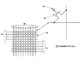
[1.本システムの構成]図2は、本発明の再構成可能信号処理システムを車両用として適用した場合の車両内ネットワークの一構成例を示す図である。図2の左上には放送受信や無線通信を行うためのアナログ回路が示され、図2の左下には画像、距離、車両速度及び加速度等を測定するためのセンサー群が示されている。また、各部のアナログ信号をディジタルデータに変換するアナログディジタルコンバータ(ADC)とネットワーク2aに接続するインターフェース(I/F)が接続されている。なお、無線通信用のアナログ回路には、ネットワーク2aからのディジタルデータをアナログ信号に変換するディジタルアナログコンバータ(DAC)も具備する。
[1. Configuration of the present system] FIG. 2 is a diagram showing a configuration example of an in-vehicle network when the reconfigurable signal processing system of the present invention is applied to a vehicle. An analog circuit for performing broadcast reception and wireless communication is shown in the upper left of FIG. 2, and a sensor group for measuring images, distance, vehicle speed, acceleration, and the like is shown in the lower left of FIG. Further, an analog / digital converter (ADC) that converts an analog signal of each part into digital data and an interface (I / F) that is connected to the
また、カーナビゲーション、インタネットのウェブ閲覧、AV(オーディオ・ビデオ)再生及びゲーム等のマルチメディア信号処理のため、CD、DVD及びHD(ハードディスク)のドライブがネットワーク2aに接続されている。さらに、ユーザインターフェースのためのディスプレイやキーボード等の入出力装置もネットワーク2aに接続されている。
Also, CD, DVD and HD (hard disk) drives are connected to the
図2の右下には、ブレーキ、ステアリング及びエンジン等の車両の主要な機械的機能を作動させるアクチュエータが、I/FとDACを介してネットワーク2aに接続されている。また、エアバックやシートベルト等のプリクラッシュシステムの機械的機能を作動させるモータやアクチュエータが、同様に接続されている。
In the lower right of FIG. 2, actuators that operate the main mechanical functions of the vehicle such as a brake, a steering, and an engine are connected to the
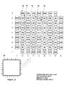
また、信号処理ユニット1〜Npがネットワーク2aに接続されている。ネットワーク2aへの接続方法は、車両の各部に分散するようにしている。図3(a)は、7個の信号処理ユニットが車両の各部に分散してネットワーク2a上に位置していることを示す一例である。各信号処理ユニット内部の概略構成の一例を図10に示す。図10では、信号処理ユニットは、再構成可能演算処理回路10aと2個のコンフィギュレーションデータメモリから構成される。再構成可能信号処理回路10aは、FPGAまたはリコンフィギュラブルプロセッサから構成される。FPGA、リコンフィギュラブルプロセッサ及びコンフィギュレーションデータについて、以下の[2.FPGAについて]で説明する。
[2.FPGAについて]FPGAのようなプログラマブルな論理回路が、近年普及しつつある。詳細な内部構成は以下の「6.FPGAの内部構成」において記載するが、FPGAは、多数のLUT(Look-up table)とスイッチがチップ上に集積されており、LUTのデータとスイッチ制御情報を外部から書き込むことによって論理回路の再構成が行われ、プロセッサを含む所望の演算処理回路を実現することができる半導体デバイスである。このデバイスを用いれば、信号処理アルゴリズムを高速に且つ最小遅延時間で実行する最適構造の演算処理回路を構築できる。 [2. About FPGA] Programmable logic circuits such as FPGA are becoming popular in recent years. The detailed internal configuration will be described in “6. Internal configuration of FPGA” below. The FPGA has many LUTs (Look-up Tables) and switches integrated on the chip, and the LUT data and switch control information. Is a semiconductor device in which a logic circuit is reconfigured by externally writing and a desired arithmetic processing circuit including a processor can be realized. By using this device, it is possible to construct an arithmetic processing circuit having an optimal structure for executing a signal processing algorithm at a high speed and with a minimum delay time.
LUTに記憶するデータやスイッチ制御情報等の書き込まれるプログラムは、コンフィギュレーションデータ(構成データ)と呼ばれる。一般的にコンフィギュレーションデータを外部から書き込むためには多数の動作クロックサイクルが必要であるが、最近ではリコンフィギュラブルプロセッサと呼ばれるコンフィギュレーションデータを数クロックで短時間に書き込みと再構成ができる半導体も開発されている。 A program in which data stored in the LUT, switch control information, or the like is written is called configuration data (configuration data). In general, a large number of operation clock cycles are required to write configuration data from the outside. Recently, there is a semiconductor called reconfigurable processor that can write and reconfigure configuration data in a few clocks in a short time. Has been developed.
「3.再構成可能信号処理ユニットの構成と故障時の復旧アルゴリズム」ここでは、ある信号処理ユニットが故障した場合に、故障した信号処理ユニットで実行していた演算回路を他の正常な信号処理ユニットに移動する手法について説明する。上述したように、信号処理ユニットは車両の各部に分散しており(図3)、各信号処理ユニットは再構成可能演算処理回路10aと2個のコンフィギュレーションデータメモリから構成される(図10)。
“3. Configuration of Reconfigurable Signal Processing Unit and Recovery Algorithm in Case of Failure” Here, when a certain signal processing unit fails, the arithmetic circuit executed in the failed signal processing unit is replaced with another normal signal processing. A method of moving to a unit will be described. As described above, the signal processing units are dispersed in each part of the vehicle (FIG. 3), and each signal processing unit is composed of a reconfigurable
ある信号処理ユニットの再構成可能演算処理回路10aのコンフィギュレーションデータは別の場所に配置された他の2個の信号処理ユニットのコンフィギュレーションデータメモリに書き込まれている。その対応を図16に示す。ユニットのID番号とは、再構成可能演算処理回路10aの実装されている信号処理ユニットの番号である。例えば、1番の信号処理ユニットの再構成可能演算処理回路10aへロードするコンフィギュレーションデータは、2番と6番の信号処理ユニットのコンフィギュレーションデータメモリに格納されている。
The configuration data of the reconfigurable
信号処理ユニットが故障した場合の復旧の方法について図11を参照しながら説明する。いま、3番の信号処理ユニットが故障したとする。3番の信号処理ユニットの再構成可能演算処理回路10aのコンフィギュレーションデータが格納されている2番及び4番の信号処理ユニットが(図16)、3番の信号処理ユニットの故障を検出する。2番及び4番の信号処理ユニットは、3番の信号処理ユニットの再構成可能演算処理回路10aのコンフィギュレーションデータをコンフィギュレーションデータメモリより読み出す。2番及び4番の信号処理ユニットは、読み出したコンフィギュレーションデータを7番の信号処理ユニットにネットワーク2aを経由して伝送することによって、その7番の信号処理ユニット内の再構成可能演算処理回路10a上に3番と同一の信号処理回路が再構成する。したがって、故障した3番の信号処理ユニットで行われていた信号処理は、7番の信号処理ユニットで継続して実行されることになる。また、3番の信号処理ユニットが故障したので、6番の信号処理ユニットの再構成可能演算処理回路10aのコンフィギュレーションデータが格納されている信号処理ユニットが、2番の信号処理ユニットだけとなり一つ減ってしまう。そこで、7番のコンフィギュレーションメモリに、6番の信号処理ユニットの再構成可能演算処理回路10aのコンフィギュレーションデータを格納することによって、故障により一つ減ってしまった状況を回復することができる。なお、7番の信号処理ユニットは、信号処理機能を持たない冗長の信号処理ユニットとして、予めネットワーク2a上に接続されているものである。
A method of recovery when the signal processing unit fails will be described with reference to FIG. Assume that the third signal processing unit has failed. The second and fourth signal processing units storing the configuration data of the reconfigurable
また、故障を検出する信号処理ユニットは、特に限定しない。例えば、6番の信号処理ユニットが、3番の信号処理ユニットの故障を検出するとともに、2番及び4番の信号処理ユニットに対し3番のコンフィギュレーションデータを7番の信号処理ユニットに伝送する指令を出すようにしてもよい。 Further, the signal processing unit for detecting a failure is not particularly limited. For example, the No. 6 signal processing unit detects a failure of the No. 3 signal processing unit, and transmits No. 3 configuration data to the No. 7 signal processing unit to the No. 2 and No. 4 signal processing units. A command may be issued.
また、上述の例では、自身のコンフィギュレーションデータが格納されているユニットの数は2個にしていた(以下、「多重化数を2にする」という)。この多重化数は、車両の走行方向と各信号処理ユニットの配置に基づいて決定される。車両が前方に走行していれば、車両フロント部に配置された信号処理ユニットは、衝突等により破損・故障する確率が高くなる。そこで、車両フロント部に配置された信号処理ユニットのコンフィギュレーションデータが格納されている信号処理ユニットの数を多くすることによって、衝突等による破損・故障に対する信頼性を向上させることができる。逆に、車両リヤ部に配置された信号処理ユニットに対しては、多重化数を減らすことも可能である。また、少なくとも2つ以上分散させておくことによって、1つのコンフィギュレーションデータメモリが故障したとしても、少なくとももう一つは残っているので、故障に対する信頼性も向上する。 In the above example, the number of units storing its own configuration data is set to two (hereinafter referred to as “the number of multiplexing is set to two”). The number of multiplexing is determined based on the traveling direction of the vehicle and the arrangement of the signal processing units. If the vehicle is traveling forward, the probability that the signal processing unit disposed in the vehicle front portion will be damaged or broken due to a collision or the like increases. Therefore, by increasing the number of signal processing units that store configuration data of signal processing units arranged in the front part of the vehicle, it is possible to improve the reliability with respect to breakage / failure due to a collision or the like. On the contrary, the number of multiplexing can be reduced for the signal processing unit arranged in the rear part of the vehicle. Also, by dispersing at least two or more, even if one configuration data memory fails, at least one more remains, so the reliability against failure is improved.
また、信号処理ユニットとその信号処理ユニットのコンフィギュレーションデータが格納されている信号処理ユニットとの位置関係は、できるだけ離したほうがよい。衝突等によって、それらが両方とも破損・故障してしまうことを避けるためである。例えば、車両フロント部に配置された2番の信号処理ユニットのコンフィギュレーションデータは、車両中間部に配置された5番及び車両リヤ部に配置された6番の信号処理ユニットに格納されている。 The positional relationship between the signal processing unit and the signal processing unit in which configuration data of the signal processing unit is stored should be as far as possible. This is to prevent both of them from being damaged or failing due to a collision or the like. For example, the configuration data of the No. 2 signal processing unit arranged in the vehicle front part is stored in No. 5 signal processing unit arranged in the vehicle middle part and No. 6 signal processing unit arranged in the vehicle rear part.
ところで、コンフィギュレーションデータをロードする前に、信号処理ユニットが正常かどうかの検査が行われる。信号処理ユニットの故障診断は、自立分散的に行われ、自らが自己診断機能を有している。再構成可能演算処理回路10aにテスト用コンフィギュレーションデータをロードする。その回路10aに対し外部から入力信号を加えて、または、回路内部で信号を発生させて、所定の参照信号と比較して一致すれば、その再構成可能演算処理回路10aは正常と判断し、図3(b)に示されるように、フラグに“OK”と表示する。一方、不一致ならば故障と判断して、フラグに“NG”を表示する。“OK”と表示されたフラグを有する信号処理ユニットに対して、コンフィギュレーションデータがロードされると、そのフラグの表示は“BUSY”に変わる。また、自己診断機能が故障していた場合には、“NG”と表示する。このようにすることによって、どの信号処理ユニットが故障しているか否か(“OK”か“NG”)、使用可能か否か(“OK”か“BUSY”)を判別することができる。なお、正常であった場合はそのユニットにロードを行い、正常でなかった場合は正常なものが見つかるまで、他のユニットのフラグを検査する。
By the way, before loading the configuration data, it is checked whether the signal processing unit is normal. The failure diagnosis of the signal processing unit is performed in a self-supporting and distributed manner and has a self-diagnosis function. The test configuration data is loaded into the reconfigurable
上記のようなネットワーク2a上を伝送するコンフィギュレーションデータやフラグ情報は、図13で示されるネットワーク伝送用パケットで伝送する。宛先アドレスは、宛先の信号処理ユニットのIDアドレス(図16にあるような信号処理ユニットのID番号)、その信号処理ユニット内部の再構成可能演算処理回路10aのIDアドレス及びその回路内の演算要素(加算器等)のIDアドレスから構成される。送信元アドレスも、送信元の信号処理ユニットに関して、上記の宛先アドレスと同様の構成である。データ部は、図2のセンサー群からの出力データ、演算結果の演算用データまたはコンフィギュレーションデータ等である。信頼性を向上させるためにCRC(Cyclic redundancy checksum)が付加される。
The configuration data and flag information transmitted on the
ネットワーク2aから信号処理ユニットに伝送されたパケットは、以下のように信号処理ユニット内で信号処理される。図14は、信号処理ユニットの構成の一例を示す図である。パケット分解部14aは、ネットワーク2aから伝送されたパケットの解析を行い、コンフィギュレーションデータ、演算入力データ若しくは読み取ったフラグの情報なのかを判別する。コンフィギュレーションデータならば、再構成可能演算処理回路14h(10a)にダウンロードを行う。演算入力データならば、その再構成された演算処理回路14hに演算データとして入力される。フラグならば、フラグ変化検出回路14iに入力される。フラグの変化によって他の信号処理ユニットが故障したことが判定される。
Packets transmitted from the
パケット分解部14aを介したデータは、テーブル14に規定された対応関係に従って、マルチプレクサDMUX14dを介して、再構成可能演算処理回路14hやコンフィギュレーションデータメモリ等に出力される。コンフィギュレーションデータメモリは、NCM個分用意される。なお、NCMは多重化数を表す。他の信号処理ユニットの故障が検出された場合には、再構成可能演算処理回路10aによる演算結果データとコンフィギュレーションデータメモリからその故障した信号処理ユニットに対応するコンフィギュレーションデータが読み出される。読み出されたそれらのデータは、マルチプレクサMUX14eを経由した後に、パケット生成部14cによって生成された図13のデータパケットでネットワーク2aに送出される。
The data via the packet decomposing unit 14a is output to the reconfigurable arithmetic processing circuit 14h, the configuration data memory, etc. via the
再構成可能演算処理回路10aの検査は、まず、テスト信号発生回路を構成するためのコンフィギュレーションデータをテスト回路14fからロードする。そして、構成されたテスト信号発生回路から出力されたデータをテスト回路14f内の参照データと比較することによって、故障しているかどうかが判定される。その結果をフラグレジスタに設定する。
In the inspection of the reconfigurable
[4.コンフィギュレーションデータのダウンロード手法]コンフィギュレーションデータを再構成可能演算処理回路10aにダウンロードすることによって、所望の回路が実現されるが、一般的なFPGAの場合、コンフィギュレーションデータのダウンロードが完了するまでにデータのビット数に依存したクロック数分の時間がかかる。たとえ1クロックで瞬時にダウンロードと再構成が完了して演算回路が切り替わったと仮定しても、ディジタル信号処理で頻繁に使用されるFIRフィルタは過去のデータを現在の出力の計算に使用するために、過去の入力データをコンフィギュレーションメモリに記憶させておく必要がある。したがって、新しく再構成が行われた直後の回路状態ではアクチュエータ等に対して送るべき出力データがしばらく現れない現象が発生する。それを解決するのが以下の手法である。
[4. Configuration Data Download Method] A desired circuit is realized by downloading the configuration data to the reconfigurable
図5は、本ダウンロード手法の一例を示す図である。簡単のために、2個のセンサー1,2、各センサーに対応する信号処理ユニット1,2若しくはアクチュエータ1,2、未使用の信号処理ユニット3及びネットワーク2aから構成される。
FIG. 5 is a diagram illustrating an example of the present download method. For simplicity, it is composed of two
図5(a)は、新しいコンフィギュレーションデータをロードする前の状態である。センサー1からの信号は、処理Aを処理する信号処理回路が搭載されている信号処理ユニット1に伝送される。信号処理ユニット1による処理Aの結果が、アクチュエータ1に伝送されて駆動する。センサー2、処理Bを処理する信号処理ユニット2及びアクチュエータ2も同様にデータが伝送される。未使用の信号処理ユニット3はネットワーク2aと制御信号の授受を行うが、データの授受を行わない。
FIG. 5A shows a state before loading new configuration data. A signal from the
いま、センサー1による信号検出からアクチュエータ1の駆動までの上記の処理Aを処理Cに代える場合について説明する。図5(b)において、まず、信号処理ユニット1または2が、未使用の信号処理ユニット3に対して、起動制御信号を伝送する。
Now, a case where the above-described processing A from signal detection by the
図5(c)において、信号処理ユニット3に対して、図16のテーブルに従って、信号処理ユニット2(もしくは、(図5上には記載していないが)信号処理ユニット4)からコンフィギュレーションデータがロードされる。そして、信号処理ユニット3は、そのコンフィギュレーションデータに基づいて再構成が行われ、処理Cを処理する信号処理回路を実現する。
In FIG. 5C, the configuration data is received from the signal processing unit 2 (or the signal processing unit 4 (not shown in FIG. 5)) according to the table of FIG. Loaded. Then, the
図5(d)において、センサー1からの信号は、処理Cを処理する信号処理ユニット3でも受信する。しかし、信号処理ユニット3による処理3の処理結果データの送信は行わない。
In FIG. 5D, the signal from the
図5(e)において、信号処理ユニット3は、処理3の処理結果データのアクチュエータ1への送信を開始する。同時に、信号処理ユニット1の動作を停止させる。
In FIG. 5 (e), the
このように、冗長な信号処理ユニットを設け、既存の処理を実行中にコンフィギュレーションデータのロードと再構成を行い、データ受信を行わせて、データ送信とともに既存の信号処理ユニットを停止させる。このように再構成を行うことによって、アクチュエータ1へのデータの流れの滞りやデータ不連続点の発生を防止する。
In this manner, a redundant signal processing unit is provided, and configuration data is loaded and reconfigured during execution of existing processing, data reception is performed, and the existing signal processing unit is stopped together with data transmission. By performing the reconfiguration in this way, the stagnation of data flow to the
[5.信号処理の切り替え方法]それでは、より具体的な信号処理ユニットの処理例について説明する。図4は、その障害物発見時の信号処理の一例を示す。この例では、ある車両が通常運転の時から衝突事故に至るまでの信号処理内容の変移が示されている。簡単のため、信号処理の種類は、走行・制動系、安全系、マルチメディアアプリケーション系の3種類とした。走行・制動系の信号処理には、通常走行のための基本的なエンジン制御、ステアリング制御及びブレーキ制御等がある。安全系の信号処理には、未然に事故を防ぐためのアクティブセーフティ関連制御等がある。マルチメディアアプリケーション(以下、MMAという)系の信号処理には、カーナビゲーションや車内エンタテイメントのためのDVD・ビデオ再生技術やブロードバンドインタネットアクセスのための超高速無線通信技術等のいわゆるマルチメディア信号処理制御がある。 [5. Signal Processing Switching Method] Now, a more specific processing example of the signal processing unit will be described. FIG. 4 shows an example of signal processing when the obstacle is found. In this example, the transition of signal processing contents from the time when a certain vehicle is in normal operation until a collision accident is shown. For simplicity, there are three types of signal processing: driving / braking system, safety system, and multimedia application system. The signal processing of the traveling / braking system includes basic engine control, steering control, and brake control for normal traveling. Safety signal processing includes active safety related control to prevent accidents. Signal processing for multimedia applications (hereinafter referred to as MMA) includes so-called multimedia signal processing control such as DVD / video playback technology for car navigation and in-car entertainment and ultra-high-speed wireless communication technology for broadband Internet access. is there.
図4の左側には信号処理のフローチャートが、右側にはそのときの信号処理ユニット全体の再構成可能演算処理回路のハードウェアリソースに対しての各アプリケーションの使用率が示されている。例えば、5つの信号処理ユニットが3つの信号処理を分担し、その使用率で処理する。もしくは、各信号処理ユニットのそれぞれがその使用率で3つの信号処理を行い、相互に協調制御すると考えてもよい。もしくは、信号処理ユニット1が走行・制動系信号処理を、信号処理ユニット2が安全系信号処理を、信号処理ユニット3がMMA系信号処理を担当し、全体としてその使用率になると考えてもよい。以下にこのフローチャートの説明を行う。
The signal processing flowchart is shown on the left side of FIG. 4, and the usage rate of each application with respect to the hardware resources of the reconfigurable arithmetic processing circuit of the entire signal processing unit at that time is shown on the right side. For example, five signal processing units share the three signal processing and process at the usage rate. Alternatively, it may be considered that each of the signal processing units performs three signal processes at the usage rate, and performs cooperative control with each other. Alternatively, it may be considered that the
通常走行時には、信号処理ユニット全体として、コンフィギュレーションデータ0がロードされている(ステップ40)。コンフィギュレーションデータ0は、カーナビゲーションやインタネット接続のためのMMA系信号処理や、エンジン・ステアリング制御等の走行・制動系信号処理の使用率が比較的使用率高い。また、安全系信号処理は低精度ではあるが、レーダーによる距離測定や障害物監視や白線レーントラッキング等のための画像処理を常に行っている。
During normal running,
MMA系信号処理は、GPS、TV・ラジオ、無線LAN・携帯電話のRF・IFアナログ回路からAD変換されたディジタルデータ、または、CD・DVD・HDドライブからのディジタルデータが,ネットワーク2aを経由して,対応する信号処理ユニットに転送された後に、スピーカーやディスプレイ等のユーザI/Fに転送されることによって行われる。
For MMA signal processing, digital data converted from the RF / IF analog circuit of GPS, TV / radio, wireless LAN / cell phone, or digital data from CD / DVD / HD drive is transmitted via the
安全系信号処理は、図2におけるカメラ、レーザーレーダー、ミリ波レーダーによって検出された外界情報が、ネットワーク2aを経由して、対応する信号処理ユニットに送信されることによって行われる。処理精度は、走行速度に依存し、高速走行の方が低速走行よりも高くなる。
The safety system signal processing is performed by transmitting external information detected by the camera, laser radar, and millimeter wave radar in FIG. 2 to the corresponding signal processing unit via the
いま、TVカメラからの画像上に障害物を検知したと仮定する(ステップ41)。安全系の測定精度を高めた信号処理を実現するコンフィギュレーションデータ1が、ネットワーク2a経由で信号処理ユニットにロードされる。この信号処理ユニットは、詳細な処理を行って(ステップ41)、その障害物に対し対策が必要なのか、または、必要ないのかを判断する(ステップ42)。
Assume that an obstacle is detected on the image from the TV camera (step 41).
対策が必要ないと判断されれば、通常走行時の回路使用状況に戻すために、再度コンフィギュレーションメモリからネットワーク2a経由でコンフィギュレーションデータ1が再度ロードされる。
If it is determined that no countermeasure is required, the
対策が必要あると判断されたならば、走行・制御系の信号処理の使用率を増加させて精度を高めた信号処理の組み合わせを実装するコンフィギュレーションデータ2が同様にロードされる(ステップ43)。これにより、ステアリングやブレーキ制御を補強して、ブレーキアシストや横滑り防止制御を起動して衝突を回避させる。このとき、図2における各車輪の速度センサー、加速度センサー、舵角センサーからの信号をネットワーク2a経由で信号処理ユニットに伝送して処理した後、ブレーキ、ステアリング、スロットルのアクチュエータが作動する。そして、コンフィギュレーションデータ2がロードされた信号処理ユニットは、衝突回避可否を判断する(ステップ44)。
If it is determined that a countermeasure is required,
センサーからの信号によって衝突が回避できたと判明すれば、通常走行時の回路使用状況に戻すために、再度コンフィギュレーションメモリからネットワーク2a経由でコンフィギュレーションデータ1が再度ロードされる。
If it is determined that the collision can be avoided by the signal from the sensor, the
センサーからの信号によって、今後、衝突が回避できないと判断したならば、コンフィギュレーションメモリよりコンフィギュレーションデータ3をロードして、プリクラッシュシステムの信号処理回路を信号処理ユニット上に実現する(ステップ45)。プリクシャッシュシステムを実現する信号処理ユニットがシートベルトモーターを駆動させてシートベルトを巻き取ることによって、乗員が速やかに拘束される。また、その信号処理ユニットがブレーキのアクチュエータを駆動させてブレーキアシストを作動させることによって、衝突速度が低減する。また、その信号処理ユニットによって、エアバックアクチュエータを駆動させてエアバックシステムを作動させることによって、乗員の衝突の衝撃が和らぐ。
If it is determined from the signal from the sensor that a collision cannot be avoided in the future, the
衝突(ステップ46)後は、コンフィギュレーションデータ4がコンフィギュレーションメモリよりロードされる(ステップ47)。これにより、衝突による故障から免れた信号処理ユニット上に、GPSや無線通信等のMMA系信号処理を実現する回路が実現し、事故現場の位置を測定して、緊急無線通信を行う。
After the collision (step 46), the
したがって、上述の信号処理ユニットの処理例をまとめると、以下のことがいえる。車両では多種多様な信号処理が行われるが、一般的に、全ての信号処理回路の稼働率が必ずしも高くはなく、必要とされる演算精度や時間的精度が必ずしも高くなければならないとも限らない。これらの要求精度は、走行状況によって変動する。 Therefore, the following can be said when processing examples of the above-described signal processing unit are summarized. Although various types of signal processing are performed in a vehicle, generally, the operation rate of all signal processing circuits is not necessarily high, and the required calculation accuracy and temporal accuracy are not necessarily high. These required accuracies vary depending on traveling conditions.
例えば、通常走行の場合には、MMA系信号処理やエンジン制御信号処理を優先するために、これらの信号処理には高い精度が要求され、ステアリングやブレーキ制御の安全系信号処理にはそれほどの高い精度は要求されない。一方、センサーによって異常が検出された場合には、優先順位の高い安全系信号処理に高い精度が要求される。 For example, in the case of normal driving, MMA system signal processing and engine control signal processing are prioritized, so high accuracy is required for these signal processing, and so much is required for safety system signal processing for steering and brake control. Precision is not required. On the other hand, when an abnormality is detected by the sensor, high accuracy is required for safety system signal processing with high priority.
したがって、本信号処理の全体の流れは、図1に示されるように、まず、センサーからのセンシングデータの入力によって走行状況を判断し(ステップ10)、現在のハードウェアリソース(使用可能ハードウェア量)情報を取得する(ステップ11)。そして、最適なコンフィギュレーションデータを選択できるように、信号処理機能の演算精度やクロック周波数を変動させる(ステップ12)。具体的には、演算回路のデータビット数を低くして演算回路規模を縮小したり、クロック周波数を低くして演算器の個数を減少したりすることによって、ハードウェアの使用率を下げる。その逆をすることによって、ハードウェア使用率を上げる。そして、図16の対応関係となるように、そのコンフィギュレーションデータが所定の信号処理ユニットにロードされ(ステップ13)、コンフィギュレーションメモリに書き込まれる(ステップ14)。その後、各信号処理ユニットがそれぞれに割り当てられた信号処理を開始する(ステップ15)。 Therefore, as shown in FIG. 1, the overall flow of this signal processing is as follows. First, the driving situation is determined by inputting sensing data from the sensor (step 10), and the current hardware resource (the amount of available hardware). ) Obtain information (step 11). Then, the calculation accuracy of the signal processing function and the clock frequency are varied so that optimum configuration data can be selected (step 12). Specifically, the hardware usage rate is reduced by reducing the number of data bits of the arithmetic circuit to reduce the scale of the arithmetic circuit or reducing the clock frequency to reduce the number of arithmetic units. The hardware usage rate is increased by doing the reverse. Then, the configuration data is loaded into a predetermined signal processing unit (step 13) and written into the configuration memory (step 14) so as to have the correspondence relationship of FIG. Thereafter, each signal processing unit starts signal processing assigned thereto (step 15).
さらに、本発明に基づく再構成可能信号処理システムの全体的な流れは、図12にまとめられる。図2のセンサー群からのセンシングデータがネットワーク2a上に送出されると(ステップ120)、そのデータに対応する処理をする信号処理ユニットがそのデータを受信する(ステップ121)。各信号処理ユニットは、図3のように、お互いのフラグを観測して、使用可能な信号処理ユニットを調査する(ステップ122)。図4のように、ハードウェアリソースに基づき、最適な信号処理回路を選択し、コンフィギュレーションデータメモリにアクセスする(ステップ123)。図16等のテーブルに基づいて、コンフィギュレーションデータの宛先となる信号処理ユニットを決定する(ステップ124)。読み出されたコンフィギュレーションデータは(ステップ125)、図13のパケット構成でネットワーク2aに送出される(ステップ126)。送出されたコンフィギュレーションデータは、宛先の信号処理ユニットの再構成可能演算処理回路にダウンロードされる(ステップ127)。いずれかの信号処理ユニットが故障した場合には、その故障した信号処理ユニットのコンフィギュレーションデータが、冗長な信号処理ユニットの再構成可能演算処理回路にダウンロードされるとともに、その故障した信号処理ユニットが格納していたコンフィギュレーションデータが、冗長な信号処理ユニットのコンフィギュレーションメモリに書き込まれる(ステップ128)。再構成可能演算処理回路にコンフィギュレーションデータがダウンロードされた信号処理ユニットは、信号処理を開始する(ステップ129)。
Furthermore, the overall flow of the reconfigurable signal processing system according to the present invention is summarized in FIG. When the sensing data from the sensor group of FIG. 2 is transmitted on the
[6.FPGAの内部構成]上述した発明を実現するために必要な、所望の信号処理機能に再構成可能な電子デバイスについて、FPGAを具体例に挙げて、以下説明する。図6は、FPGAの内部構成の一例である。まず、FPGAチップ6aには外部からコンフィギュレーションデータが供給され、コンフィギュレーションデータメモリに書き込まれる。コンフィギュレーションデータメモリは、図6上では図示されていない。コンフィギュレーションデータメモリは、後述するが、FPGAを構成する各ブロックに分散されている。このコンフィギュレーションデータによって各部の機能がプログラムされる。プログラム可能な論理回路ブロックであるCLB(Configurable logic block)6bは、対応するコンフィギュレーションデータによって、ユーザが所望する小規模な論理回路に構成できる。説明をわかりやすくするために、図6では3×3のCLBから構成されるFPGAを示しているが、実際には数十×数十ものCLBが集積される比較的大規模な構成のFPGAもある。
[6. Internal Configuration of FPGA] An electronic device that can be reconfigured to have a desired signal processing function necessary for realizing the above-described invention will be described below using an FPGA as a specific example. FIG. 6 shows an example of the internal configuration of the FPGA. First, configuration data is supplied from the outside to the
IOB(Input/output blocks)6cは、チップ外とチップ内の信号のインターフェース回路であり、一種の電流増幅器でもある。対応するコンフィギュレーションデータによって所定の論理振幅電圧に設定され、外部論理電圧を内部の論理電圧に変換する機能を有する。 An IOB (Input / Output blocks) 6c is an interface circuit for signals outside and inside the chip, and is also a kind of current amplifier. A predetermined logic amplitude voltage is set by corresponding configuration data and has a function of converting an external logic voltage into an internal logic voltage.
RC(Routing channel)6dは、各ブロック接続するデータバスである。プログラム可能なスイッチであるCB(Connection block)6eとSB(Switch block)6fはマトリクス状に配置される。CBは、CLBとCLBの間、SBとSBの間及びCLBとIOBの間の接続を行う。SBは、CBとCBの間及びCBとIOBの間の接続を行う。 An RC (Routing channel) 6d is a data bus connected to each block. CB (Connection block) 6e and SB (Switch block) 6f, which are programmable switches, are arranged in a matrix. The CB performs connections between CLB and CLB, between SB and SB, and between CLB and IOB. The SB performs connection between CB and CB and between CB and IOB.
なお、図6ではコンフィギュレーションデータのコンフィギュレーションメモリへの入力と分配を行うハードウェア構成の図示は省略している。 In FIG. 6, a hardware configuration for inputting and distributing configuration data to the configuration memory is not shown.
図7は、CLBの内部構成の一例を示す。CLBは、4入力1出力のLUT7a,7b、3入力1出力のLUT7c、キャリ生成専用のプログラム可能な論理回路であるCL(Carry logic)7d,7e、9個のマルチプレクサ(7f〜7n)及び2個のレジスタ7o,7pから構成される。CLBはSRAM(Static Random Access Memory)であり、入力はアドレスに相当する。4入力と3入力のLUTには、それぞれ16ビットと8ビットのコンフィギュレーションデータをダウンロードして任意の論理回路を構成することができる。さらに、各マルチプレクサの制御信号を貯えるコンフィギュレーションメモリ7qも具備している。
FIG. 7 shows an example of the internal configuration of the CLB. The CLB includes four-input one-
図15は、4入力のLUTの真理値表の一例を示す図である。CLは、対応するコンフィギュレーションデータによって、あらかじめ定義されているいくつかの論理回路の一つを実現できる。また、各マルチプレクサの制御信号もコンフィギュレーションデータによって設定される。種々のコンフィギュレーションデータをCLBに与えることによってレジスタを含む所望の論理回路を実現することができる。 FIG. 15 is a diagram illustrating an example of a truth table of a 4-input LUT. The CL can realize one of several logic circuits defined in advance by corresponding configuration data. The control signal for each multiplexer is also set by configuration data. A desired logic circuit including a register can be realized by supplying various configuration data to the CLB.
図8は、SBの構成例を示す。バス8a,8b,8c,8dはそれぞれ上下左右に配置されている。スイッチ8eは各バスのビット線の交差点に対角線上に配置され、入力は4方向のビット線に接続される。スイッチの4方向からの各ビット線間にトランジスタ8fのソースとドレインが接続されている。ドランジスタのゲートにはコンフィギュレーションメモリのセル8gが接続され、セルに書き込まれた信号によって4方向のビット線のオン・オフ制御を行う。なお、コンフィギュレーションメモリへの入力信号や制御信号の記述は省略している。
FIG. 8 shows a configuration example of the SB. The
図9は、CBの構成例を示す。図中、上下に配置されているバス9aはSBに接続されるバスである。交差した左側のバス9bと右側のバス9cはIOB又はCLBに接続されるバスである。スイッチ9dは、各バスのビット線に接続され、各ビット線間にトランジスタ9eのソースとドレインが接続され、そのドランジスタのゲート電圧を制御する信号はコンフィギュレーションメモリのセル9fに書き込まれている。セルの信号によってトランジスタのオン・オフ制御を行う。なお、コンフィギュレーションメモリへ書き込むデータ信号や制御信号の記述は省略している。
FIG. 9 shows a configuration example of the CB. In the figure, the
IOBも同様に、内部のコンフィギュレーションメモリのセルのデータによって、入出力信号の電圧レベル、出力電流の最大値、レジスタの挿入・非挿入等の設定が行われる。 Similarly, in the IOB, the voltage level of the input / output signal, the maximum value of the output current, the insertion / non-insertion of the register, and the like are set according to the data of the cells in the internal configuration memory.
以上のように、コンフィギュレーションメモリに所望の回路を実現するデータを書き込むことによって、CB,SB,CLB,IOBに対するプログラムが行われ、所望の仕様の論理回路をFPGA上に実現できる。図2のネットワーク2a経由でコンフィギュレーションデータが図7のコンフィギュレーショメモリへロードされる。回路の再構成時間はその転送時間とメモリの書き込み時間に依存する。リコンフィギュラブルプロセッサの構成においては、コンフィギュレーションメモリを複数用意して、出力を切り替えることによって一瞬に回路を再構成できる。さらに、演算単位も粒度の細かいLUTのみならず、ビット幅の比較的大きい論理または数値演算を行う粒度の荒いプログラマブル演算器も複数用意している場合もある。
As described above, by writing data for realizing a desired circuit in the configuration memory, a program for CB, SB, CLB, and IOB is performed, and a logic circuit having a desired specification can be realized on the FPGA. Configuration data is loaded into the configuration memory of FIG. 7 via the
以上、本発明の好ましい実施例について詳説したが、本発明は、上述した実施例に制限されることはなく、本発明の範囲を逸脱することなく、上述した実施例に種々の変形及び置換を加えることができる。 The preferred embodiments of the present invention have been described in detail above. However, the present invention is not limited to the above-described embodiments, and various modifications and substitutions can be made to the above-described embodiments without departing from the scope of the present invention. Can be added.
上述の実施例では、車両での適用について詳細な説明をしたが、本発明は、船舶、飛行機及びロボット等にも適用可能である。 In the above-described embodiments, the application in the vehicle has been described in detail, but the present invention can also be applied to ships, airplanes, robots, and the like.
2a ネットワーク
10a 再構成可能演算処理回路
Claims (6)
所望の信号処理機能に再構成可能な電子デバイスと、
前記信号処理ユニットの故障を検出する故障検出手段と、
前記電子デバイスを前記信号処理ユニットの信号処理機能に再構成する構成データを記憶する記憶手段とを備え、
前記記憶手段に記憶された構成データに基づいて前記故障検出手段により故障が検出された前記信号処理ユニットの信号処理機能に前記電子デバイスを再構成する再構成可能信号処理システムにおいて、
前記信号処理ユニットと前記電子デバイスとを含むネットワーク上に前記記憶手段を少なくとも2つ以上分散させたことを特徴とする再構成可能信号処理システム。 A signal processing unit having a predetermined signal processing function;
An electronic device reconfigurable to a desired signal processing function;
Failure detection means for detecting a failure of the signal processing unit;
Storage means for storing configuration data for reconfiguring the electronic device into a signal processing function of the signal processing unit;
In the reconfigurable signal processing system for reconfiguring the electronic device to the signal processing function of the signal processing unit in which a failure is detected by the failure detection means based on the configuration data stored in the storage means,
A reconfigurable signal processing system, wherein at least two storage units are distributed on a network including the signal processing unit and the electronic device.
前記故障検出手段により前記電子デバイスの故障が無いと検出された後に、該電子デバイスの再構成を行う請求項1記載の再構成可能信号処理システム。 The failure detection means further detects the presence or absence of a failure of the electronic device,
The reconfigurable signal processing system according to claim 1, wherein the electronic device is reconfigured after the failure detection means detects that the electronic device has no failure.
Priority Applications (1)
| Application Number | Priority Date | Filing Date | Title |
|---|---|---|---|
| JP2004344064A JP4422596B2 (en) | 2004-11-29 | 2004-11-29 | Reconfigurable signal processing system |
Applications Claiming Priority (1)
| Application Number | Priority Date | Filing Date | Title |
|---|---|---|---|
| JP2004344064A JP4422596B2 (en) | 2004-11-29 | 2004-11-29 | Reconfigurable signal processing system |
Publications (2)
| Publication Number | Publication Date |
|---|---|
| JP2006155176A true JP2006155176A (en) | 2006-06-15 |
| JP4422596B2 JP4422596B2 (en) | 2010-02-24 |
Family
ID=36633412
Family Applications (1)
| Application Number | Title | Priority Date | Filing Date |
|---|---|---|---|
| JP2004344064A Expired - Fee Related JP4422596B2 (en) | 2004-11-29 | 2004-11-29 | Reconfigurable signal processing system |
Country Status (1)
| Country | Link |
|---|---|
| JP (1) | JP4422596B2 (en) |
Cited By (5)
| Publication number | Priority date | Publication date | Assignee | Title |
|---|---|---|---|---|
| US8090982B2 (en) | 2007-06-11 | 2012-01-03 | Toyota Jidosha Kabushiki Kaisha | Multiprocessor system enabling controlling with specific processor under abnormal operation and control method thereof |
| JP2012502837A (en) * | 2008-09-19 | 2012-02-02 | ボンバルディア トランスポーテイション ゲーエムベーハー | Unstable monitoring devices and systems, especially for rail vehicles |
| WO2015005224A1 (en) * | 2013-07-08 | 2015-01-15 | ヤマハ株式会社 | Signal processing system and program |
| WO2018230149A1 (en) * | 2017-06-12 | 2018-12-20 | 日立オートモティブシステムズ株式会社 | Electronic control device, vehicle-mounted system, and power supply device |
| CN112098959A (en) * | 2019-10-31 | 2020-12-18 | 上海交通大学 | Reconfigurable radar target/interference simulator based on FPGA and implementation method |
Families Citing this family (1)
| Publication number | Priority date | Publication date | Assignee | Title |
|---|---|---|---|---|
| US11385977B2 (en) | 2017-04-25 | 2022-07-12 | Hitachi, Ltd. | Reconfiguration control device |
Citations (4)
| Publication number | Priority date | Publication date | Assignee | Title |
|---|---|---|---|---|
| JPH07334382A (en) * | 1994-06-07 | 1995-12-22 | Hitachi Ltd | Multicontroller system |
| JPH0844581A (en) * | 1994-07-29 | 1996-02-16 | Fujitsu Ltd | Information processor with self-repairing function |
| JP2000181566A (en) * | 1998-12-14 | 2000-06-30 | Mitsubishi Electric Corp | Multiclock parallel processor |
| JP2003115847A (en) * | 2001-10-09 | 2003-04-18 | Denso Corp | Control system and redundant signal processor |
-
2004
- 2004-11-29 JP JP2004344064A patent/JP4422596B2/en not_active Expired - Fee Related
Patent Citations (4)
| Publication number | Priority date | Publication date | Assignee | Title |
|---|---|---|---|---|
| JPH07334382A (en) * | 1994-06-07 | 1995-12-22 | Hitachi Ltd | Multicontroller system |
| JPH0844581A (en) * | 1994-07-29 | 1996-02-16 | Fujitsu Ltd | Information processor with self-repairing function |
| JP2000181566A (en) * | 1998-12-14 | 2000-06-30 | Mitsubishi Electric Corp | Multiclock parallel processor |
| JP2003115847A (en) * | 2001-10-09 | 2003-04-18 | Denso Corp | Control system and redundant signal processor |
Cited By (8)
| Publication number | Priority date | Publication date | Assignee | Title |
|---|---|---|---|---|
| US8090982B2 (en) | 2007-06-11 | 2012-01-03 | Toyota Jidosha Kabushiki Kaisha | Multiprocessor system enabling controlling with specific processor under abnormal operation and control method thereof |
| JP2012502837A (en) * | 2008-09-19 | 2012-02-02 | ボンバルディア トランスポーテイション ゲーエムベーハー | Unstable monitoring devices and systems, especially for rail vehicles |
| WO2015005224A1 (en) * | 2013-07-08 | 2015-01-15 | ヤマハ株式会社 | Signal processing system and program |
| WO2018230149A1 (en) * | 2017-06-12 | 2018-12-20 | 日立オートモティブシステムズ株式会社 | Electronic control device, vehicle-mounted system, and power supply device |
| JP2019003284A (en) * | 2017-06-12 | 2019-01-10 | 日立オートモティブシステムズ株式会社 | Electronic control device, on-vehicle system, and power supply device |
| US11192507B2 (en) | 2017-06-12 | 2021-12-07 | Hitachi Astemo, Ltd. | Electronic control device, in-vehicle system, and power supply device |
| CN112098959A (en) * | 2019-10-31 | 2020-12-18 | 上海交通大学 | Reconfigurable radar target/interference simulator based on FPGA and implementation method |
| CN112098959B (en) * | 2019-10-31 | 2023-11-14 | 上海交通大学 | Reconfigurable radar target/interference simulator based on FPGA and implementation method |
Also Published As
| Publication number | Publication date |
|---|---|
| JP4422596B2 (en) | 2010-02-24 |
Similar Documents
| Publication | Publication Date | Title |
|---|---|---|
| JP7034987B2 (en) | Power and data center (PDC) for automotive applications | |
| EP3724763B1 (en) | System and method for online functional testing for error-correcting code function | |
| US9917725B2 (en) | Automotive neural network | |
| JP3049048B2 (en) | Emulation module | |
| US7873773B2 (en) | Multi-node architecture with daisy chain communication link configurable to operate in unidirectional and bidirectional modes | |
| JP3965410B2 (en) | Redundant vehicle control device | |
| US10445285B2 (en) | Integrated data concentrator for multi-sensor MEMS systems | |
| CN110447015B (en) | Vehicle-mounted control device for redundantly executing operating functions and corresponding motor vehicle | |
| JP2008538151A (en) | System and method for dynamically optimizing the performance and reliability of a redundant processing system | |
| CN111025959A (en) | Data management method, device and equipment and intelligent automobile | |
| JP4422596B2 (en) | Reconfigurable signal processing system | |
| JP6802374B2 (en) | Vehicle control device and vehicle control system | |
| JPH06180675A (en) | Method and apparatus for inspecting validity of bus configuration of multiple-source disk array bus | |
| WO2018123205A1 (en) | Microcomputer and logical circuit | |
| US20220144298A1 (en) | Device for providing image data | |
| US20210208899A1 (en) | Data processing system and method for configuring and operating a data processing system | |
| Channon et al. | The requirements of future in-vehicle networks and an example implementation | |
| JP2021060764A (en) | Driving control device | |
| JP3141472B2 (en) | Switching control method | |
| JP7164483B2 (en) | Electronic controller, control system | |
| US20240134730A1 (en) | Safety monitoring of a system-on-a-chip | |
| JP7106237B2 (en) | vehicle controller | |
| CN114930312A (en) | Communication method and related device | |
| JP2020052479A (en) | Vehicle controller and vehicle control method | |
| JP3315375B2 (en) | Signal transmission system |
Legal Events
| Date | Code | Title | Description |
|---|---|---|---|
| A621 | Written request for application examination |
Free format text: JAPANESE INTERMEDIATE CODE: A621 Effective date: 20070125 |
|
| A977 | Report on retrieval |
Free format text: JAPANESE INTERMEDIATE CODE: A971007 Effective date: 20090123 |
|
| A131 | Notification of reasons for refusal |
Free format text: JAPANESE INTERMEDIATE CODE: A131 Effective date: 20090203 |
|
| A521 | Written amendment |
Free format text: JAPANESE INTERMEDIATE CODE: A523 Effective date: 20090325 |
|
| TRDD | Decision of grant or rejection written | ||
| A01 | Written decision to grant a patent or to grant a registration (utility model) |
Free format text: JAPANESE INTERMEDIATE CODE: A01 Effective date: 20091117 |
|
| A01 | Written decision to grant a patent or to grant a registration (utility model) |
Free format text: JAPANESE INTERMEDIATE CODE: A01 |
|
| A61 | First payment of annual fees (during grant procedure) |
Free format text: JAPANESE INTERMEDIATE CODE: A61 Effective date: 20091204 |
|
| FPAY | Renewal fee payment (event date is renewal date of database) |
Free format text: PAYMENT UNTIL: 20121211 Year of fee payment: 3 |
|
| FPAY | Renewal fee payment (event date is renewal date of database) |
Free format text: PAYMENT UNTIL: 20121211 Year of fee payment: 3 |
|
| FPAY | Renewal fee payment (event date is renewal date of database) |
Free format text: PAYMENT UNTIL: 20121211 Year of fee payment: 3 |
|
| FPAY | Renewal fee payment (event date is renewal date of database) |
Free format text: PAYMENT UNTIL: 20131211 Year of fee payment: 4 |
|
| LAPS | Cancellation because of no payment of annual fees |