JP2006148100A - Formation technology for low-dielectric-constant nanoparticle film - Google Patents
Formation technology for low-dielectric-constant nanoparticle film Download PDFInfo
- Publication number
- JP2006148100A JP2006148100A JP2005329871A JP2005329871A JP2006148100A JP 2006148100 A JP2006148100 A JP 2006148100A JP 2005329871 A JP2005329871 A JP 2005329871A JP 2005329871 A JP2005329871 A JP 2005329871A JP 2006148100 A JP2006148100 A JP 2006148100A
- Authority
- JP
- Japan
- Prior art keywords
- gas
- plasma discharge
- organic
- reactor
- nanoparticles
- Prior art date
- Legal status (The legal status is an assumption and is not a legal conclusion. Google has not performed a legal analysis and makes no representation as to the accuracy of the status listed.)
- Withdrawn
Links
- 239000002105 nanoparticle Substances 0.000 title claims abstract description 115
- 230000015572 biosynthetic process Effects 0.000 title claims description 22
- 238000005516 engineering process Methods 0.000 title abstract 2
- 239000007789 gas Substances 0.000 claims abstract description 195
- 238000000034 method Methods 0.000 claims abstract description 82
- 239000000758 substrate Substances 0.000 claims abstract description 65
- 239000011261 inert gas Substances 0.000 claims abstract description 28
- 239000010419 fine particle Substances 0.000 claims description 53
- 229910052710 silicon Inorganic materials 0.000 claims description 27
- 229930195733 hydrocarbon Natural products 0.000 claims description 24
- XUIMIQQOPSSXEZ-UHFFFAOYSA-N Silicon Chemical compound [Si] XUIMIQQOPSSXEZ-UHFFFAOYSA-N 0.000 claims description 23
- 239000012495 reaction gas Substances 0.000 claims description 22
- 238000000151 deposition Methods 0.000 claims description 21
- 239000010703 silicon Substances 0.000 claims description 20
- 239000004215 Carbon black (E152) Substances 0.000 claims description 19
- 150000002430 hydrocarbons Chemical class 0.000 claims description 14
- 230000008569 process Effects 0.000 claims description 12
- 229910052799 carbon Inorganic materials 0.000 claims description 6
- 230000008021 deposition Effects 0.000 claims description 6
- 238000010438 heat treatment Methods 0.000 claims description 6
- 230000001590 oxidative effect Effects 0.000 claims description 6
- 229910052734 helium Inorganic materials 0.000 claims description 5
- 239000011859 microparticle Substances 0.000 claims description 5
- 238000009832 plasma treatment Methods 0.000 claims description 5
- OKTJSMMVPCPJKN-UHFFFAOYSA-N Carbon Chemical compound [C] OKTJSMMVPCPJKN-UHFFFAOYSA-N 0.000 claims description 4
- 229910052786 argon Inorganic materials 0.000 claims description 4
- 125000001183 hydrocarbyl group Chemical group 0.000 claims 10
- 239000012528 membrane Substances 0.000 claims 2
- 238000010168 coupling process Methods 0.000 abstract description 4
- 238000007599 discharging Methods 0.000 abstract 1
- 208000028659 discharge Diseases 0.000 description 78
- 239000002245 particle Substances 0.000 description 55
- 230000002776 aggregation Effects 0.000 description 30
- 238000004220 aggregation Methods 0.000 description 23
- 238000009792 diffusion process Methods 0.000 description 21
- 239000000463 material Substances 0.000 description 16
- 239000012071 phase Substances 0.000 description 10
- 238000005054 agglomeration Methods 0.000 description 7
- 230000000694 effects Effects 0.000 description 7
- 238000006243 chemical reaction Methods 0.000 description 6
- 238000005268 plasma chemical vapour deposition Methods 0.000 description 6
- JJQZDUKDJDQPMQ-UHFFFAOYSA-N dimethoxy(dimethyl)silane Chemical compound CO[Si](C)(C)OC JJQZDUKDJDQPMQ-UHFFFAOYSA-N 0.000 description 5
- 238000010790 dilution Methods 0.000 description 4
- 239000012895 dilution Substances 0.000 description 4
- 239000003990 capacitor Substances 0.000 description 3
- 238000009833 condensation Methods 0.000 description 3
- 230000005494 condensation Effects 0.000 description 3
- 238000002474 experimental method Methods 0.000 description 3
- 239000012212 insulator Substances 0.000 description 3
- 238000000790 scattering method Methods 0.000 description 3
- 229910052724 xenon Inorganic materials 0.000 description 3
- 101000694017 Homo sapiens Sodium channel protein type 5 subunit alpha Proteins 0.000 description 2
- 229910020175 SiOH Inorganic materials 0.000 description 2
- 230000015271 coagulation Effects 0.000 description 2
- 238000005345 coagulation Methods 0.000 description 2
- 230000008878 coupling Effects 0.000 description 2
- 238000005859 coupling reaction Methods 0.000 description 2
- 238000009826 distribution Methods 0.000 description 2
- 229910052739 hydrogen Inorganic materials 0.000 description 2
- 238000012625 in-situ measurement Methods 0.000 description 2
- 238000011065 in-situ storage Methods 0.000 description 2
- 239000000203 mixture Substances 0.000 description 2
- 229910052760 oxygen Inorganic materials 0.000 description 2
- 239000004065 semiconductor Substances 0.000 description 2
- 229910018540 Si C Inorganic materials 0.000 description 1
- 125000004429 atom Chemical group 0.000 description 1
- 238000004364 calculation method Methods 0.000 description 1
- 239000011248 coating agent Substances 0.000 description 1
- 238000000576 coating method Methods 0.000 description 1
- 239000012141 concentrate Substances 0.000 description 1
- 239000004020 conductor Substances 0.000 description 1
- 239000000470 constituent Substances 0.000 description 1
- 238000001816 cooling Methods 0.000 description 1
- 230000007423 decrease Effects 0.000 description 1
- 230000003247 decreasing effect Effects 0.000 description 1
- 238000005137 deposition process Methods 0.000 description 1
- 238000010586 diagram Methods 0.000 description 1
- 239000011521 glass Substances 0.000 description 1
- 230000005764 inhibitory process Effects 0.000 description 1
- 239000011229 interlayer Substances 0.000 description 1
- 238000003475 lamination Methods 0.000 description 1
- 238000004519 manufacturing process Methods 0.000 description 1
- 238000005259 measurement Methods 0.000 description 1
- 238000000691 measurement method Methods 0.000 description 1
- 238000010297 mechanical methods and process Methods 0.000 description 1
- 230000007246 mechanism Effects 0.000 description 1
- 238000012544 monitoring process Methods 0.000 description 1
- 150000002894 organic compounds Chemical group 0.000 description 1
- 125000004430 oxygen atom Chemical group O* 0.000 description 1
- 230000010287 polarization Effects 0.000 description 1
- 239000002243 precursor Substances 0.000 description 1
- 238000012545 processing Methods 0.000 description 1
- 239000010453 quartz Substances 0.000 description 1
- 230000035484 reaction time Effects 0.000 description 1
- VYPSYNLAJGMNEJ-UHFFFAOYSA-N silicon dioxide Inorganic materials O=[Si]=O VYPSYNLAJGMNEJ-UHFFFAOYSA-N 0.000 description 1
- 238000003892 spreading Methods 0.000 description 1
- 230000007480 spreading Effects 0.000 description 1
- 230000001629 suppression Effects 0.000 description 1
- 239000012808 vapor phase Substances 0.000 description 1
- 238000001947 vapour-phase growth Methods 0.000 description 1
Images


Classifications
-
- C—CHEMISTRY; METALLURGY
- C23—COATING METALLIC MATERIAL; COATING MATERIAL WITH METALLIC MATERIAL; CHEMICAL SURFACE TREATMENT; DIFFUSION TREATMENT OF METALLIC MATERIAL; COATING BY VACUUM EVAPORATION, BY SPUTTERING, BY ION IMPLANTATION OR BY CHEMICAL VAPOUR DEPOSITION, IN GENERAL; INHIBITING CORROSION OF METALLIC MATERIAL OR INCRUSTATION IN GENERAL
- C23C—COATING METALLIC MATERIAL; COATING MATERIAL WITH METALLIC MATERIAL; SURFACE TREATMENT OF METALLIC MATERIAL BY DIFFUSION INTO THE SURFACE, BY CHEMICAL CONVERSION OR SUBSTITUTION; COATING BY VACUUM EVAPORATION, BY SPUTTERING, BY ION IMPLANTATION OR BY CHEMICAL VAPOUR DEPOSITION, IN GENERAL
- C23C16/00—Chemical coating by decomposition of gaseous compounds, without leaving reaction products of surface material in the coating, i.e. chemical vapour deposition [CVD] processes
- C23C16/44—Chemical coating by decomposition of gaseous compounds, without leaving reaction products of surface material in the coating, i.e. chemical vapour deposition [CVD] processes characterised by the method of coating
- C23C16/50—Chemical coating by decomposition of gaseous compounds, without leaving reaction products of surface material in the coating, i.e. chemical vapour deposition [CVD] processes characterised by the method of coating using electric discharges
- C23C16/505—Chemical coating by decomposition of gaseous compounds, without leaving reaction products of surface material in the coating, i.e. chemical vapour deposition [CVD] processes characterised by the method of coating using electric discharges using radio frequency discharges
- C23C16/509—Chemical coating by decomposition of gaseous compounds, without leaving reaction products of surface material in the coating, i.e. chemical vapour deposition [CVD] processes characterised by the method of coating using electric discharges using radio frequency discharges using internal electrodes
-
- C—CHEMISTRY; METALLURGY
- C23—COATING METALLIC MATERIAL; COATING MATERIAL WITH METALLIC MATERIAL; CHEMICAL SURFACE TREATMENT; DIFFUSION TREATMENT OF METALLIC MATERIAL; COATING BY VACUUM EVAPORATION, BY SPUTTERING, BY ION IMPLANTATION OR BY CHEMICAL VAPOUR DEPOSITION, IN GENERAL; INHIBITING CORROSION OF METALLIC MATERIAL OR INCRUSTATION IN GENERAL
- C23C—COATING METALLIC MATERIAL; COATING MATERIAL WITH METALLIC MATERIAL; SURFACE TREATMENT OF METALLIC MATERIAL BY DIFFUSION INTO THE SURFACE, BY CHEMICAL CONVERSION OR SUBSTITUTION; COATING BY VACUUM EVAPORATION, BY SPUTTERING, BY ION IMPLANTATION OR BY CHEMICAL VAPOUR DEPOSITION, IN GENERAL
- C23C16/00—Chemical coating by decomposition of gaseous compounds, without leaving reaction products of surface material in the coating, i.e. chemical vapour deposition [CVD] processes
- C23C16/22—Chemical coating by decomposition of gaseous compounds, without leaving reaction products of surface material in the coating, i.e. chemical vapour deposition [CVD] processes characterised by the deposition of inorganic material, other than metallic material
- C23C16/30—Deposition of compounds, mixtures or solid solutions, e.g. borides, carbides, nitrides
- C23C16/40—Oxides
- C23C16/401—Oxides containing silicon
-
- H—ELECTRICITY
- H01—ELECTRIC ELEMENTS
- H01L—SEMICONDUCTOR DEVICES NOT COVERED BY CLASS H10
- H01L21/00—Processes or apparatus adapted for the manufacture or treatment of semiconductor or solid state devices or of parts thereof
- H01L21/02—Manufacture or treatment of semiconductor devices or of parts thereof
- H01L21/02104—Forming layers
- H01L21/02107—Forming insulating materials on a substrate
- H01L21/02109—Forming insulating materials on a substrate characterised by the type of layer, e.g. type of material, porous/non-porous, pre-cursors, mixtures or laminates
- H01L21/02112—Forming insulating materials on a substrate characterised by the type of layer, e.g. type of material, porous/non-porous, pre-cursors, mixtures or laminates characterised by the material of the layer
- H01L21/02123—Forming insulating materials on a substrate characterised by the type of layer, e.g. type of material, porous/non-porous, pre-cursors, mixtures or laminates characterised by the material of the layer the material containing silicon
- H01L21/02126—Forming insulating materials on a substrate characterised by the type of layer, e.g. type of material, porous/non-porous, pre-cursors, mixtures or laminates characterised by the material of the layer the material containing silicon the material containing Si, O, and at least one of H, N, C, F, or other non-metal elements, e.g. SiOC, SiOC:H or SiONC
-
- H—ELECTRICITY
- H01—ELECTRIC ELEMENTS
- H01L—SEMICONDUCTOR DEVICES NOT COVERED BY CLASS H10
- H01L21/00—Processes or apparatus adapted for the manufacture or treatment of semiconductor or solid state devices or of parts thereof
- H01L21/02—Manufacture or treatment of semiconductor devices or of parts thereof
- H01L21/02104—Forming layers
- H01L21/02107—Forming insulating materials on a substrate
- H01L21/02109—Forming insulating materials on a substrate characterised by the type of layer, e.g. type of material, porous/non-porous, pre-cursors, mixtures or laminates
- H01L21/02203—Forming insulating materials on a substrate characterised by the type of layer, e.g. type of material, porous/non-porous, pre-cursors, mixtures or laminates the layer being porous
-
- H—ELECTRICITY
- H01—ELECTRIC ELEMENTS
- H01L—SEMICONDUCTOR DEVICES NOT COVERED BY CLASS H10
- H01L21/00—Processes or apparatus adapted for the manufacture or treatment of semiconductor or solid state devices or of parts thereof
- H01L21/02—Manufacture or treatment of semiconductor devices or of parts thereof
- H01L21/02104—Forming layers
- H01L21/02107—Forming insulating materials on a substrate
- H01L21/02109—Forming insulating materials on a substrate characterised by the type of layer, e.g. type of material, porous/non-porous, pre-cursors, mixtures or laminates
- H01L21/02205—Forming insulating materials on a substrate characterised by the type of layer, e.g. type of material, porous/non-porous, pre-cursors, mixtures or laminates the layer being characterised by the precursor material for deposition
- H01L21/02208—Forming insulating materials on a substrate characterised by the type of layer, e.g. type of material, porous/non-porous, pre-cursors, mixtures or laminates the layer being characterised by the precursor material for deposition the precursor containing a compound comprising Si
- H01L21/02214—Forming insulating materials on a substrate characterised by the type of layer, e.g. type of material, porous/non-porous, pre-cursors, mixtures or laminates the layer being characterised by the precursor material for deposition the precursor containing a compound comprising Si the compound comprising silicon and oxygen
- H01L21/02216—Forming insulating materials on a substrate characterised by the type of layer, e.g. type of material, porous/non-porous, pre-cursors, mixtures or laminates the layer being characterised by the precursor material for deposition the precursor containing a compound comprising Si the compound comprising silicon and oxygen the compound being a molecule comprising at least one silicon-oxygen bond and the compound having hydrogen or an organic group attached to the silicon or oxygen, e.g. a siloxane
-
- H—ELECTRICITY
- H01—ELECTRIC ELEMENTS
- H01L—SEMICONDUCTOR DEVICES NOT COVERED BY CLASS H10
- H01L21/00—Processes or apparatus adapted for the manufacture or treatment of semiconductor or solid state devices or of parts thereof
- H01L21/02—Manufacture or treatment of semiconductor devices or of parts thereof
- H01L21/02104—Forming layers
- H01L21/02107—Forming insulating materials on a substrate
- H01L21/02225—Forming insulating materials on a substrate characterised by the process for the formation of the insulating layer
- H01L21/0226—Forming insulating materials on a substrate characterised by the process for the formation of the insulating layer formation by a deposition process
- H01L21/02263—Forming insulating materials on a substrate characterised by the process for the formation of the insulating layer formation by a deposition process deposition from the gas or vapour phase
- H01L21/02271—Forming insulating materials on a substrate characterised by the process for the formation of the insulating layer formation by a deposition process deposition from the gas or vapour phase deposition by decomposition or reaction of gaseous or vapour phase compounds, i.e. chemical vapour deposition
- H01L21/02274—Forming insulating materials on a substrate characterised by the process for the formation of the insulating layer formation by a deposition process deposition from the gas or vapour phase deposition by decomposition or reaction of gaseous or vapour phase compounds, i.e. chemical vapour deposition in the presence of a plasma [PECVD]
-
- H—ELECTRICITY
- H01—ELECTRIC ELEMENTS
- H01L—SEMICONDUCTOR DEVICES NOT COVERED BY CLASS H10
- H01L21/00—Processes or apparatus adapted for the manufacture or treatment of semiconductor or solid state devices or of parts thereof
- H01L21/02—Manufacture or treatment of semiconductor devices or of parts thereof
- H01L21/02104—Forming layers
- H01L21/02107—Forming insulating materials on a substrate
- H01L21/02225—Forming insulating materials on a substrate characterised by the process for the formation of the insulating layer
- H01L21/0226—Forming insulating materials on a substrate characterised by the process for the formation of the insulating layer formation by a deposition process
- H01L21/02263—Forming insulating materials on a substrate characterised by the process for the formation of the insulating layer formation by a deposition process deposition from the gas or vapour phase
- H01L21/02271—Forming insulating materials on a substrate characterised by the process for the formation of the insulating layer formation by a deposition process deposition from the gas or vapour phase deposition by decomposition or reaction of gaseous or vapour phase compounds, i.e. chemical vapour deposition
- H01L21/0228—Forming insulating materials on a substrate characterised by the process for the formation of the insulating layer formation by a deposition process deposition from the gas or vapour phase deposition by decomposition or reaction of gaseous or vapour phase compounds, i.e. chemical vapour deposition deposition by cyclic CVD, e.g. ALD, ALE, pulsed CVD
-
- H—ELECTRICITY
- H01—ELECTRIC ELEMENTS
- H01L—SEMICONDUCTOR DEVICES NOT COVERED BY CLASS H10
- H01L21/00—Processes or apparatus adapted for the manufacture or treatment of semiconductor or solid state devices or of parts thereof
- H01L21/02—Manufacture or treatment of semiconductor devices or of parts thereof
- H01L21/02104—Forming layers
- H01L21/02107—Forming insulating materials on a substrate
- H01L21/02296—Forming insulating materials on a substrate characterised by the treatment performed before or after the formation of the layer
- H01L21/02318—Forming insulating materials on a substrate characterised by the treatment performed before or after the formation of the layer post-treatment
- H01L21/02337—Forming insulating materials on a substrate characterised by the treatment performed before or after the formation of the layer post-treatment treatment by exposure to a gas or vapour
- H01L21/0234—Forming insulating materials on a substrate characterised by the treatment performed before or after the formation of the layer post-treatment treatment by exposure to a gas or vapour treatment by exposure to a plasma
-
- H—ELECTRICITY
- H01—ELECTRIC ELEMENTS
- H01L—SEMICONDUCTOR DEVICES NOT COVERED BY CLASS H10
- H01L21/00—Processes or apparatus adapted for the manufacture or treatment of semiconductor or solid state devices or of parts thereof
- H01L21/02—Manufacture or treatment of semiconductor devices or of parts thereof
- H01L21/04—Manufacture or treatment of semiconductor devices or of parts thereof the devices having at least one potential-jump barrier or surface barrier, e.g. PN junction, depletion layer or carrier concentration layer
- H01L21/18—Manufacture or treatment of semiconductor devices or of parts thereof the devices having at least one potential-jump barrier or surface barrier, e.g. PN junction, depletion layer or carrier concentration layer the devices having semiconductor bodies comprising elements of Group IV of the Periodic System or AIIIBV compounds with or without impurities, e.g. doping materials
- H01L21/30—Treatment of semiconductor bodies using processes or apparatus not provided for in groups H01L21/20 - H01L21/26
- H01L21/31—Treatment of semiconductor bodies using processes or apparatus not provided for in groups H01L21/20 - H01L21/26 to form insulating layers thereon, e.g. for masking or by using photolithographic techniques; After treatment of these layers; Selection of materials for these layers
- H01L21/314—Inorganic layers
- H01L21/316—Inorganic layers composed of oxides or glassy oxides or oxide based glass
- H01L21/31695—Deposition of porous oxides or porous glassy oxides or oxide based porous glass
Abstract
Description
本発明は、シリコンを含有するガスを使用して、プラズマCVD法により、絶縁性のSiOCHまたはSiCの組成を持つ直径数ナノの粒子を気相中に形成し、これらの粒子をウエハー上に堆積することにより多孔質構造を持つ低誘電率の膜を形成する技術に関する。 In the present invention, by using a gas containing silicon, particles having a diameter of several nanometers having a composition of insulating SiOCH or SiC are formed in a gas phase by plasma CVD, and these particles are deposited on a wafer. The present invention relates to a technique for forming a low dielectric constant film having a porous structure.
デバイスノードの縮小と共に、そのデバイスに使われる層間絶縁膜には次の表に示すように低い比誘電率(Low-k)が求められる。 As the device node shrinks, the interlayer dielectric used for the device is required to have a low dielectric constant (Low-k) as shown in the following table.
適用時期 デバイスノード k
2003 90 nm 2.9 - 3.1
2005 65 nm 2.6 - 2.8
2007 45 nm 2.2 - 2.4
誘電率が2.7程度のLow-k膜についてはCVD法と塗布法など数多くの膜形成法が提案され良質なLow-k膜の形成が近年可能となり、デバイスノードが90nmノードの量産デバイスへの適用が始まっている。次世代の高速デバイスとしてk=2.5程度以下のさらに低い誘電率のLow-k膜が求められている。
Applicable time Device node k
2003 90 nm 2.9-3.1
2005 65 nm 2.6-2.8
2007 45 nm 2.2-2.4
For low-k films with a dielectric constant of about 2.7, many film-forming methods such as CVD and coating have been proposed, and high-quality low-k films can be formed in recent years, and they can be applied to mass-produced devices with a device node of 90 nm. Has begun. As a next-generation high-speed device, a low-k film having a lower dielectric constant of about k = 2.5 or less is required.
その一つとして、ナノ粒子を形成し基板上に堆積させることで低誘電率膜を形成する方法が知られている。例えば、米国特許第6,737,366号、米国特許第6,602,800号に上下電極の間に中間電極を設け、反応器を上下空間に分離し、下部空間でのプラズマ発生を抑制することにより、電荷の発生を低減し、ナノ粒子が電荷の影響を受けずに基板に積層しやすくする技術が開示されている。また、米国特許第 6,537,928号には中間電極に加え更に冷却プレートを中間電極とサセプタの間に配置することにより、下部空間の温度を低く制御し、ナノ粒子が水分を利用して基板上に積層しやすくする技術が開示されている。
本発明は、ナノ粒子の発生自体を制御し、効果的に基板上に堆積させる技術である。即ち、プラズマCVDによりSi含有ガスから絶縁性微粒子を気相中で形成し、凝集を抑制しながら、基板表面まで有効に輸送し基板上に低誘電率膜を形成する技術を提供する。 The present invention is a technique for controlling the generation of nanoparticles itself and depositing them effectively on a substrate. That is, the present invention provides a technique for forming insulating fine particles from a Si-containing gas in a gas phase by plasma CVD, effectively transporting them to the substrate surface while suppressing aggregation, and forming a low dielectric constant film on the substrate.
ある形態によれば、本発明は、(I)有機Siガスと不活性ガスからなる反応ガスを容量結合方式のCVD装置の反応器へ導入する工程、(II)該有機Siガスから気相中に生成する微粒子のサイズを該反応器内におけるプラズマ放電時間の関数として、nmオーダーに調整する工程、及び(III)生成した該微粒子を該反応器内に載置された基板上に堆積する工程、を包含する、低誘電率膜を形成する方法、を提供する。 According to a certain aspect, the present invention provides (I) a step of introducing a reaction gas composed of an organic Si gas and an inert gas into a reactor of a capacitively coupled CVD apparatus, and (II) a gas phase from the organic Si gas in the gas phase. Adjusting the size of the generated fine particles to a nanometer order as a function of plasma discharge time in the reactor; and (III) depositing the generated fine particles on a substrate placed in the reactor. A method of forming a low dielectric constant film is provided.
上記の形態は以下の態様を少なくとも包含するが、本発明はそれら態様に限定されるものではない。 The above forms include at least the following aspects, but the present invention is not limited to these aspects.
該有機Siガスの流量は該不活性ガスの流量に対して10%以下でよく、該有機Siガスの流量は該不活性ガスの流量に対して5%以下でよく、該プラズマ放電は約8W/cm2から約13W/cm2のRF電力を印加することにより実施してもよく、プラズマ放電中の反応器内圧力は約0.1 Torr から約 10 Torrとしてもよく、また、該反応ガスの流速が該反応器内の電極面に平行な方向(一般には基板面と平行方向)で2.5cm/秒以下となるように調整てもよい。成膜中の基板温度は約0℃から約450℃の範囲としてもよい。 The flow rate of the organic Si gas may be 10% or less with respect to the flow rate of the inert gas, the flow rate of the organic Si gas may be 5% or less with respect to the flow rate of the inert gas, and the plasma discharge is about 8 W. / cm 2 to about 13 W / cm 2 by applying RF power, the pressure in the reactor during plasma discharge may be about 0.1 Torr to about 10 Torr, and the flow rate of the reaction gas May be adjusted to 2.5 cm / second or less in a direction parallel to the electrode surface in the reactor (generally in a direction parallel to the substrate surface). The substrate temperature during film formation may range from about 0 ° C. to about 450 ° C.
また、該プラズマ放電を13.56 MHz, 27 MHz, 60 MHzのRF電力を用いて実施してもよく、プラズマ放電を100 MHz以上のVHF帯の高周波電力を用いて実施してもよい。なお、該VHF帯の高周波電力を、スポークアンテナ電極により印加してもよい。また、プラズマ放電をRF電力の印加により実施し、RF電力のインピーダンスを電子式RF整合機により調整してもよい。 Further, the plasma discharge may be performed using RF power of 13.56 MHz, 27 MHz, and 60 MHz, and the plasma discharge may be performed using high-frequency power in a VHF band of 100 MHz or higher. The high frequency power in the VHF band may be applied by a spoke antenna electrode. Further, plasma discharge may be performed by applying RF power, and the impedance of the RF power may be adjusted by an electronic RF matching machine.
該有機SiガスはSiαOα−1R2α−β+2(OCnH2n+1)β:ここで、αは1〜3の整数、βは0, 1,2 ,3 または4、 n は1〜3の整数、RはSiに結合するC1-6 炭化水素で表されるもの、SiR4−α(OCnH2n+1)α :ここでαは0, 1,2 ,3 または 4、n は1〜3の整数、RはSiに結合するC1-6 炭化水素で表されるもの、Si2OR6−α(OCnH2n+1)α:ここでαは0, 1,2 ,3 または4、nは1〜3の整数、RはSiに結合するC1-6 炭化水素で表されるもの、SiHβR4−α(OCnH2n+1)α−β:ここでαは0, 1,2 ,3 または4、βは0, 1,2 ,3 または4、nは1または2、RはSiに結合するC1-6 炭化水素で表されるものを包含し、例えば、Si(CH3)4、Si(CH3)3(OCH3)、Si(CH3)2(OCH3)2、Si(CH3)(OCH3)3、Si(OCH3)4、Si(CH3)3(OC2H5)、Si(CH3)2(OC2H5)2、Si(CH3)(OC2H5)3、Si(OC2H5)4、SiH(CH3)3、SiH2(CH3)2、SiH3(CH3)の一つまたは、この複数の組み合わせを包含する。 The organic Si gas is Si α O α-1 R 2α-β + 2 (OC n H 2n + 1 ) β : where α is an integer of 1 to 3, β is 0, 1, 2, 3 or 4, n is An integer of 1 to 3, R is represented by C 1-6 hydrocarbon bonded to Si, SiR 4-α (OC n H 2n + 1 ) α : where α is 0, 1, 2, 3 or 4, n is an integer of 1 to 3, R is a C 1-6 hydrocarbon bonded to Si, Si 2 OR 6-α (OC n H 2n + 1 ) α : where α is 0, 1, 2, 3 or 4, n is an integer of 1 to 3, R is a C 1-6 hydrocarbon bonded to Si, SiH β R 4-α (OC n H 2n + 1 ) α- β : where α is 0, 1, 2, 3 or 4, β is 0, 1, 2, 3 or 4, n is 1 or 2, and R is a C 1-6 hydrocarbon bonded to Si For example, Si (CH 3 ) 4 , Si (CH 3 ) 3 (OCH 3 ), Si (CH 3 ) 2 (OCH 3 ) 2 , Si (CH 3 ) (OCH 3 ) 3 , Si (CH OCH 3 ) 4 , Si (CH 3 ) 3 (OC 2 H 5 ), Si (CH 3 ) 2 (OC 2 H 5 ) 2 , Si (CH 3 ) (OC 2 H 5 ) 3 , Si (OC 2 H Five ) 4 , SiH (CH 3 ) 3, SiH 2 (CH 3 ) 2 , SiH 3 (CH 3 ), or a combination thereof.
また、不活性ガスとしてArまたはHe、Ne、Kr、Xe、N2のひとつまたはその組み合わせを用いてもよい。該反応ガスが更に、生成膜のカーボン濃度を調整するためのO2、CO, CO2, N2Oの少なくとも一つを含む酸化性ガスを含有してもよい。 Further, Ar or He, Ne, Kr, Xe, or N 2 or a combination thereof may be used as the inert gas. The reaction gas may further contain an oxidizing gas containing at least one of O 2 , CO, CO 2 , and N 2 O for adjusting the carbon concentration of the generated film.
更に、一回のプラズマ放電時間を約1m秒から約1 秒として微粒子を形成してもよく、該微粒子を該基板上に堆積させる間、プラズマ放電を中止してもよい。あるいは、一回のプラズマ放電時間を約10m秒から約1秒として微粒子を形成し、一回のプラズマ放電後約100m秒から約2秒の間プラズマ放電を中止し該微粒子を該基板上へ堆積させる工程を一サイクルとし、少なくとも2回以上を実施してもよい。 Further, the fine particles may be formed with a single plasma discharge time of about 1 ms to about 1 second, and the plasma discharge may be stopped while the fine particles are deposited on the substrate. Alternatively, fine particles are formed with a single plasma discharge time of about 10 milliseconds to about 1 second, and after a single plasma discharge, the plasma discharge is stopped for about 100 milliseconds to about 2 seconds, and the fine particles are deposited on the substrate. The process of making it into one cycle may be carried out at least twice.
上記の間欠的放電処理(パルス放電)の場合、該反応ガスは該反応器内に設けられたシャワープレートのガスノズルを通って導入され、プラズマ放電は上下電極間で行われ、基板は下部電極上に載置されている構造において、流量を次の関係式を満足するように調整してもよい。 In the case of the above intermittent discharge treatment (pulse discharge), the reaction gas is introduced through a gas nozzle of a shower plate provided in the reactor, plasma discharge is performed between the upper and lower electrodes, and the substrate is placed on the lower electrode. The flow rate may be adjusted so as to satisfy the following relational expression.

N:シャワープレートのガスノズルの個数
A:シャワープレートのガスノズルの断面積(cm2)
P:反応器内の圧力(Torr)
L:電極間隔(cm)
なお、放電をパルス状にするか、しないかに拘わらず、ガス流をパルス状としてもよく、ナノ粒子が生成された後の基板への輸送時にガス流が増大するように調整してもよい。
N: Number of shower plate gas nozzles
A: Shower plate gas nozzle cross section (cm 2 )
P: Reactor pressure (Torr)
L: Electrode spacing (cm)
Regardless of whether the discharge is pulsed or not, the gas flow may be pulsed, and may be adjusted to increase the gas flow during transport to the substrate after the nanoparticles are generated. .
なお、後処理として、成膜後、プラズマ処理、UV、またはEBのいずれか、あるいはその組み合わせによる熱処理によりキュアする工程を含み、膜の機械的強度を改善することができ、また、成膜後、有機シリコンガス雰囲気に該基板を放置し、有機シリコン分子を該膜上に付着させる工程、および該膜をキュアする工程を含み、膜強度を改善してもよく、あるいは、成膜後、H2Oガス雰囲気に放置する工程と有機シリコンガス雰囲気に放置する工程を一回または複数回繰り返す工程を含み、膜強度の改善してもよい。 Note that the post-treatment includes a step of curing by heat treatment by plasma treatment, UV, EB, or a combination thereof after film formation, and the mechanical strength of the film can be improved. The film strength may be improved by leaving the substrate in an organic silicon gas atmosphere and depositing organic silicon molecules on the film, and curing the film. The step of leaving in a 2 O gas atmosphere and the step of leaving in an organic silicon gas atmosphere may be repeated one or more times to improve the film strength.
別の形態では、本発明は、(I)有機Siガスと不活性ガスからなる反応ガスを反応器内に設けられたシャワープレートのガスノズルを通して該反応器内に導入する工程、(II)反応ガス流量を次の関係式を満足するように調整する工程、 In another form, the present invention provides (I) a step of introducing a reaction gas comprising an organic Si gas and an inert gas into the reactor through a gas nozzle of a shower plate provided in the reactor, and (II) a reaction gas. Adjusting the flow rate to satisfy the following relational expression,
N:シャワープレートのガスノズルの個数
A:シャワープレートのガスノズルの断面積(cm2)
P:反応器内の圧力(Torr)
L:電極間隔(cm)
(III)該有機Siガスから気相中に生成する微粒子のサイズを該反応器内におけるプラズマ放電時間の関数として、約10nm以下に調整する工程、及び(IV)プラズマ放電を中止し生成した該微粒子を該反応器内に載置された基板上に堆積する工程、を包含する、低誘電率膜を形成する方法を提供する。
N: Number of shower plate gas nozzles
A: Shower plate gas nozzle cross section (cm 2 )
P: Reactor pressure (Torr)
L: Electrode spacing (cm)
(III) adjusting the size of the fine particles generated in the gas phase from the organic Si gas as a function of the plasma discharge time in the reactor to about 10 nm or less; and (IV) the generated by stopping the plasma discharge. Depositing fine particles on a substrate mounted in the reactor, and providing a method of forming a low dielectric constant film.
上記の形態は上記のいずれの態様も包含し得るが、少なくとも次の態様を包含する。本発明はこれらの実施態様に限定されるものではなく、また、上記、下記の実施態様は実施が可能である限りいずれも相互に置換可能なものである。 The above forms can include any of the above aspects, but at least include the following aspects. The present invention is not limited to these embodiments, and the above-described embodiments described below can be substituted for each other as long as they can be implemented.
また、一回のプラズマ放電時間を約10m秒から約1秒として微粒子を形成し、一回のプラズマ放電後約100m秒から約2秒の間プラズマ放電を中止し該微粒子を該基板上へ堆積させる工程を一サイクルとし、少なくとも2回以上を実施してもよく、該サイクルを30回から150回連続に繰り返して低誘電膜を形成してもよい。目的とする膜厚により適宜調整すればよく5サイクル、50サイクル、100サイクル等を含むいろいろな範囲で実施できる。なお、一回の実施(繰り返しなし)であってもよい。 Also, fine particles are formed with a single plasma discharge time of about 10 milliseconds to about 1 second, and after a single plasma discharge, plasma discharge is stopped for about 100 milliseconds to about 2 seconds, and the fine particles are deposited on the substrate. The process to be performed may be one cycle and may be performed at least twice, or the cycle may be repeated from 30 to 150 times to form a low dielectric film. What is necessary is just to adjust suitably with the target film thickness, and it can implement in various ranges including 5 cycles, 50 cycles, 100 cycles, etc. Note that it may be performed once (without repetition).
更に、別の形態によれば、本発明は、(A)有機Siガスと不活性ガスからなる反応ガスを反応器へ導入する工程、(B)プラズマ放電を実施し該有機Siガスから微粒子を形成する工程、及び(C)該微粒子が形成されている約100m秒から約2秒の間に該微粒子を該反応器内に載置された基板上へ堆積させる工程、を包含する、低誘電率膜を形成する方法を提供する。 Further, according to another embodiment, the present invention provides (A) a step of introducing a reaction gas composed of an organic Si gas and an inert gas into the reactor, and (B) performing plasma discharge to remove fine particles from the organic Si gas. And (C) depositing the microparticles on a substrate mounted in the reactor for about 100 milliseconds to about 2 seconds during which the microparticles are formed. A method for forming a rate film is provided.
また、上記のある態様においては、該反応器内の電極面に平行な方向のガス流速を約2.5cm/秒以下とし、所定の膜厚が得られるまでプラズマ放電及びガス流を連続的に実施する。 In one embodiment, the gas flow rate in the direction parallel to the electrode surface in the reactor is set to about 2.5 cm / second or less, and the plasma discharge and the gas flow are continuously performed until a predetermined film thickness is obtained. carry out.
上記の形態は上記のいずれの態様も包含し得るが、少なくとも次の態様を包含する。本発明はこれらの実施態様に限定されるものではなく、また、上記、下記の実施態様は実施が可能である限りいずれも相互に置換可能なものである。 The above forms can include any of the above aspects, but at least include the following aspects. The present invention is not limited to these embodiments, and the above-described embodiments described below can be substituted for each other as long as they can be implemented.
また、本発明の別の形態によれば、(A)有機Siガスと不活性ガスからなる反応ガスを反応器へ導入し、該有機Siガスからナノ粒子を形成するためプラズマ放電を実施する工程、及び(B)該有機Siガスからナノ粒子が形成される時間(T1)、形成されたナノ粒子が該反応器内に載置された基板上まで輸送される時間(T2)、ナノ粒子同士が輸送中に凝集成長を起こす時間(T3)を、プラズマ放電時間とガス流量の関数として制御し、ナノ粒子を該基板上に堆積する工程、を包含する、低誘電率膜を形成する方法を提供する。 According to another aspect of the present invention, (A) a step of introducing a reaction gas composed of an organic Si gas and an inert gas into a reactor, and performing plasma discharge to form nanoparticles from the organic Si gas. And (B) time for forming nanoparticles from the organic Si gas (T1), time for transporting the formed nanoparticles to the substrate placed in the reactor (T2), and between the nanoparticles A method of forming a low dielectric constant film, comprising: controlling a time (T3) during which the material undergoes cohesive growth during transport as a function of a plasma discharge time and a gas flow rate, and depositing nanoparticles on the substrate. provide.
上記において、ある態様では、概ねT1=0.1〜1秒、T2<T3となるように制御する。これを実現するには、例えばプラズマ放電をパルス状とし一回の放電ON時間を約0.1秒から約1秒、放電OFF時間を約10m秒から約100m秒とし、その間にナノ粒子が基板上に輸送されるようにする(パルス放電)。プラズマ放電を中止している間はナノ粒子の静電気力は作用しないためナノ粒子はガス流速とほど同じ速度で基板上まで輸送される。また、その間にナノ粒子の凝集成長が進行する。プラズマ放電中はナノ粒子は帯電しその静電気力がガス流速による粘性力に抵抗するため粒子成長領域に滞留しやすい。従って、この場合は、ナノ粒子の成長過程と輸送過程を分けて考えることができ、ナノ粒子の形成に必要なだけプラズマ放電を実施し、その後は、形成したナノ粒子の凝集成長が進む前に放電を中止し粒子を開放して基板上まで輸送するようにガス流量を調整すればよい。 In the above, in a certain aspect, control is performed so that T1 = 0.1 to 1 second and T2 <T3. In order to achieve this, for example, the plasma discharge is pulsed, the discharge ON time for one time is about 0.1 seconds to about 1 second, the discharge OFF time is about 10 milliseconds to about 100 milliseconds, during which the nanoparticles are placed on the substrate. Be transported (pulse discharge). Since the electrostatic force of the nanoparticles does not act while the plasma discharge is stopped, the nanoparticles are transported onto the substrate at the same speed as the gas flow rate. In the meantime, the aggregation growth of the nanoparticles proceeds. During the plasma discharge, the nanoparticles are charged and their electrostatic force resists the viscous force due to the gas flow velocity, so they tend to stay in the particle growth region. Therefore, in this case, the growth process and the transport process of the nanoparticles can be considered separately, and plasma discharge is performed as much as necessary for the formation of the nanoparticles, and after that, before the aggregation growth of the formed nanoparticles proceeds. The gas flow rate may be adjusted so that the discharge is stopped and the particles are released and transported to the substrate.
また、ある態様では、概ねT1=0.1〜1秒、T1=T2、T3=0となるように制御する。これを実現するには、例えばプラズマ放電を連続とし(凝集成長はプラズマ放電中は抑制されているので無視できる)、ナノ粒子が適当なサイズになった時点で基板上に到達するようにする。この場合は、ナノ粒子の形成過程と輸送過程を分けて考えることはできない。ナノ粒子の形成中に輸送されることになる。なお、輸送中もプラズマ放電が継続されるので、ナノ粒子を輸送するには比較的大きな速度(電極面に垂直方向)のガス流が必要となる。 In some embodiments, control is performed so that T1 = 0.1 to 1 second, T1 = T2, and T3 = 0. In order to realize this, for example, the plasma discharge is made continuous (can be ignored because the cohesive growth is suppressed during the plasma discharge), and the nanoparticles reach the substrate when the size becomes appropriate. In this case, the nanoparticle formation process and the transport process cannot be considered separately. It will be transported during the formation of the nanoparticles. In addition, since plasma discharge is continued during transportation, a relatively large velocity (perpendicular to the electrode surface) of gas flow is required to transport the nanoparticles.
該微粒子の平均サイズは約1nmから約10nmであってもよい。該生成された膜の誘電率は2.4以下であってもよく、該生成された膜の空孔率は約40%から約80%であってもよい。 The average size of the microparticles may be from about 1 nm to about 10 nm. The generated film may have a dielectric constant of 2.4 or less, and the generated film may have a porosity of about 40% to about 80%.
なお、本願で説明する目的、効果等の記述は本発明を限定する意図で記載されたものではない。本発明の少なくともある実施態様においてはそれらの目的、効果を達成し得るが、他の実施態様においては異なる目的、効果を達成するものであってもよい。 It should be noted that the description of the purpose, effect, etc. described in the present application is not intended to limit the present invention. In at least some embodiments of the present invention, those objects and effects can be achieved, but in other embodiments, different objects and effects may be achieved.
以下に本発明における最良の実施形態につき説明するが、本発明はこれらに限定されるものではない。当業者であれば下記の実施態様に基づきそれらに変更、修正を加え他の条件において同様の要領で実施することができる。 BEST MODE FOR CARRYING OUT THE INVENTION The best mode for carrying out the present invention will be described below, but the present invention is not limited thereto. A person skilled in the art can carry out the same procedure under other conditions by changing or modifying them based on the following embodiments.
プラズマCVDで絶縁性微粒子を形成する場合、粒子生成が起こる条件ではRF電力が局所的に集中し易く、その結果、粒子が過度に成長し10nm以下の絶縁性微粒子を気相中で安定に形成する事は一般に困難である。なお、本発明において、ナノ粒子は粒径が約1nmから数十nmの粒子であり、好ましくは粒径が約1nmから約20nmの粒子、更に好ましくは10nm以下の粒子である。また、ナノ粒子は個々の粒子だけでなく粒子群をも意味し、粒子群では構成粒子の全てがナノ粒子であることが望ましいが、それに限らず、粒度分布を有し粒子の平均径が約1nmから約10nmである粒子群が好ましい。 When forming insulating fine particles by plasma CVD, RF power tends to concentrate locally under conditions where particle generation occurs, and as a result, the particles grow excessively and stably form insulating fine particles of 10 nm or less in the gas phase. It is generally difficult to do. In the present invention, the nanoparticles are particles having a particle size of about 1 nm to several tens of nm, preferably particles having a particle size of about 1 nm to about 20 nm, and more preferably particles having a particle size of 10 nm or less. Nanoparticles mean not only individual particles but also particle groups. In the particle groups, it is desirable that all of the constituent particles are nanoparticles, but not limited to this, it has a particle size distribution and an average particle diameter of about Particle groups that are 1 nm to about 10 nm are preferred.
本発明のある態様によれば、材料ガスとして有機Si含有ガスを使い該ガスの希釈比率(材料ガス流量の全ガス流量に対する比率)を低減する(例えば5%以下)と共にガス圧を例えば約0.5Torr以上に上げ、放電領域でのガス流速(電極面に平行方向)を例えば約2.5cm/秒以下に下げ気相中でナノ粒子が形成するための反応時間を確保する一方、生成したナノ粒子が凝集しない時間内で放電し、なおかつ放電を高いRF電力(例えば約4 W/cm2以上)を電極間に印加することで実施することにより、気相中で粒子を形成し、基板上に堆積させる。 According to an aspect of the present invention, an organic Si-containing gas is used as a material gas, and a dilution ratio of the gas (a ratio of a material gas flow rate to a total gas flow rate) is reduced (for example, 5% or less) and a gas pressure is set to, for example, about 0. The gas flow rate in the discharge region (in the direction parallel to the electrode surface) is lowered to, for example, about 2.5 cm / sec or less to ensure the reaction time for forming nanoparticles in the gas phase, while generating the gas flow rate. Discharge within a time when nanoparticles do not agglomerate, and discharge is performed by applying high RF power (for example, about 4 W / cm 2 or more) between the electrodes to form particles in the gas phase, and the substrate Deposit on top.
上記の実施態様における制御パラメータには、材料ガスの希釈比率、流速、流量、反応器内圧力、RF電圧、放電時間、が含まれる。 The control parameters in the above embodiment include the dilution ratio of the material gas, the flow rate, the flow rate, the pressure in the reactor, the RF voltage, and the discharge time.
なお、成膜の制御は、上記の制御パラメータの更に上位の制御パラメータにより実施することもできる。前述したように、ナノ粒子による低誘電率膜の形成方法のある態様によれば、(A)有機Siガスと不活性ガスからなる反応ガスを反応器へ導入し、該有機Siガスからナノ粒子を形成するためプラズマ放電を実施する工程、及び(B)該有機Siガスからナノ粒子が形成される時間(T1)、形成されたナノ粒子が該反応器内に載置された基板上まで輸送される時間(T2)、ナノ粒子同士が輸送中に凝集成長を起こす時間(T3)を制御パラメータとして、該基板上へのナノ粒子の堆積を制御する工程、を包含する。従って、ある態様においては、上記時間T1、T2、T3により制御することができる。 It should be noted that the film formation control can also be performed by a higher-order control parameter than the above control parameters. As described above, according to an aspect of the method for forming a low dielectric constant film using nanoparticles, (A) a reaction gas composed of an organic Si gas and an inert gas is introduced into a reactor, and nanoparticles are formed from the organic Si gas. And (B) the time during which nanoparticles are formed from the organic Si gas (T1), and the formed nanoparticles are transported onto the substrate placed in the reactor. And the step of controlling the deposition of nanoparticles on the substrate using the time (T3) during which the nanoparticles undergo aggregation and growth during transportation as a control parameter. Therefore, in a certain aspect, it can control by the said time T1, T2, T3.
ナノ粒子のサイズを制御するには、プラズマ中のナノ粒子の粒子成長領域(プラズマシース境界で定義される領域近傍)の滞在時間を制御することが必要となる。その一例では、概ねT1=0.1〜1秒、T2<T3となるように制御する。これを実現するには、例えばプラズマ放電時間とガス流をサブパラメータとして以下のようにして達成することができる。プラズマ放電をパルス状とし一回の放電ON時間を約0.1秒から約1秒、放電OFF時間を約10m秒から約100m秒とし、その間にナノ粒子が基板上に輸送されるようにする。プラズマ放電を中止している間はナノ粒子の静電気力は作用しないためナノ粒子はガス流速とほど同じ速度で基板上まで輸送される。また、その間にナノ粒子の凝集成長が進行する。プラズマ放電中はナノ粒子は帯電しその静電気力がガス流速による粘性力に抵抗するため粒子成長領域に滞留しやすい。即ち、放電中は粒子は粒子成長領域(シース領域)に捕捉されやすい。また、プラズマ中で帯電したナノ粒子は粒子間のクーロン反発により凝集は抑制されている。従って、この場合は、ナノ粒子の成長過程と輸送過程を分けて考えることができ、ナノ粒子の形成に必要なだけプラズマ放電を実施し、その後は、放電を中止しシースを消失して形成したナノ粒子の凝集成長が進む前に基板上まで輸送するようにガス流量を調整すればよい。 In order to control the size of the nanoparticles, it is necessary to control the residence time of the particle growth region (near the region defined by the plasma sheath boundary) of the nanoparticles in the plasma. In one example, control is performed so that T1 = 0.1 to 1 second and T2 <T3. To achieve this, for example, plasma discharge time and gas flow can be achieved as sub-parameters as follows. The plasma discharge is pulsed, and the discharge ON time for one time is about 0.1 seconds to about 1 second, and the discharge OFF time is about 10 milliseconds to about 100 milliseconds, during which the nanoparticles are transported onto the substrate. Since the electrostatic force of the nanoparticles does not act while the plasma discharge is stopped, the nanoparticles are transported onto the substrate at the same speed as the gas flow rate. In the meantime, the aggregation growth of the nanoparticles proceeds. During the plasma discharge, the nanoparticles are charged and their electrostatic force resists the viscous force due to the gas flow velocity, so they tend to stay in the particle growth region. That is, during discharge, particles are easily trapped in the particle growth region (sheath region). In addition, aggregation of the nanoparticles charged in the plasma is suppressed by Coulomb repulsion between the particles. Therefore, in this case, the growth process and transport process of the nanoparticles can be considered separately, and plasma discharge was performed as much as necessary to form the nanoparticles, and then the discharge was stopped and the sheath disappeared. The gas flow rate may be adjusted so that the nanoparticles are transported to the substrate before the aggregation growth of the nanoparticles proceeds.
なお、ナノ粒子の帯電による静電気力はサイズが小さいほど小さい。従って、ガス流が早いと粒子成長領域で成長する前に該領域を出てしまう微粒子の数が多くなる。成長を開始した微粒子は帯電による静電気力を強め該領域に滞留しやすくなる。このことから基板上に堆積するナノ粒子はある範囲の粒度分布を持ったものとなり、サイズが0.1nm未満のものは堆積し難くなる。小さいサイズの粒子を堆積させたい場合は、ナノ粒子の成長速度を早くするか、ガス流速を遅くするとよい。 The electrostatic force due to charging of the nanoparticles is smaller as the size is smaller. Therefore, if the gas flow is fast, the number of fine particles that exit the region before growing in the particle growth region increases. The fine particles that have started to grow are more likely to stay in the region by increasing the electrostatic force due to charging. For this reason, nanoparticles deposited on the substrate have a certain range of particle size distribution, and particles having a size of less than 0.1 nm are difficult to deposit. If it is desired to deposit small sized particles, the nanoparticle growth rate can be increased or the gas flow rate can be decreased.
また、以下で説明するが、凝集成長はガス中の材料ガスの種類、濃度等の関数であるが、標準条件として凝集成長時間を約0.1秒として扱っても一般的には処理上の大きな支障が生ずることはない。 As will be described below, cohesive growth is a function of the type and concentration of the material gas in the gas. However, even if the coagulation growth time is treated as about 0.1 seconds as a standard condition, it is generally a major problem in processing. Will not occur.
一方、上記以外の例では、概ねT1=0.1〜1秒、T1=T2、T3=0となるように制御する。これを実現するには、例えばプラズマ放電時間とガス流をサブパラメータとして以下のようにして達成することができる。即ち、上記のパルス放電ではなく、連続放電により実施するもので、プラズマ放電を連続とし(凝集成長はプラズマ放電中は粒子間のクーロン反発により抑制されているので無視できる)、ナノ粒子が粒子成長領域で適当なサイズになった後、基板上に到達するようにする。この場合は、粒子成長領域のシースが存在し続けているので、粒子は静電気力よりも大きなガス流による粘性力が必要となる。パルス放電のようにナノ粒子の形成過程と輸送過程を分けて考えることはできない。従って、比較的大きなガス流が必要であり、静電気力を超えてナノ粒子を輸送するため、粒子の輸送速度はガス流速よりも低くなる。ガス流の粘性力がナノ粒子の静電気力よりも必要なだけ大きくなるようなガス流速(電極面に垂直)としては例えば電極間隔を約0.2秒、約0.1秒、約0.05秒、約0.025秒(前記の間の数値を含む)となる速度である。これは例えば電極間隔が40cmの場合は、約20cm/秒、約40cm/秒、約80cm/秒、約160cm/秒に相当する。 On the other hand, in examples other than the above, control is performed so that T1 = 0.1 to 1 second, T1 = T2, and T3 = 0. To achieve this, for example, plasma discharge time and gas flow can be achieved as sub-parameters as follows. That is, instead of the pulse discharge described above, the discharge is performed by continuous discharge. The plasma discharge is continuous (coagulation growth can be ignored because it is suppressed by coulomb repulsion between particles during plasma discharge), and the nanoparticles grow. After reaching an appropriate size in the area, it reaches the substrate. In this case, since the sheath of the particle growth region continues to exist, the particle needs a viscous force due to a gas flow larger than the electrostatic force. Unlike the pulse discharge, the nanoparticle formation process and the transport process cannot be considered separately. Therefore, a relatively large gas flow is required, and the transport rate of the particles is lower than the gas flow rate because the nanoparticles are transported beyond the electrostatic force. The gas flow rate (perpendicular to the electrode surface) is such that the viscous force of the gas flow is greater than the electrostatic force of the nanoparticles, for example, the electrode interval is about 0.2 seconds, about 0.1 seconds, about 0.05 seconds, about 0.025 seconds ( (Including numerical values between the above). For example, when the electrode interval is 40 cm, this corresponds to about 20 cm / second, about 40 cm / second, about 80 cm / second, and about 160 cm / second.
以下、その他のパラメータにつき説明する。特記しない限りパラメータはパルス放電と連続放電で共通である。 Hereinafter, other parameters will be described. Unless otherwise specified, the parameters are common to pulse discharge and continuous discharge.
材料ガスの希釈比率は、Ar等の不活性ガスによる高密度プラズマを維持するため低くする。材料ガスの比率が大きくなるとプラズマ密度が低下しナノ粒子の形成に必要なラジカル密度に達しなくなる場合がある。不活性ガスとしては ArまたはHe, Ne, Kr, Xe, N2のひとつまたはその組み合わせを用いることができる。材料ガスの希釈比率は例えば、約0.1%から約40%(0.2%、0.5%、1%、2%、3%、4%、5%、10%、20%、及び前記数値の間の数値を含み)、好ましくは約0.3%から約8%、更には約0.5%から約3%である。 The dilution ratio of the material gas is lowered in order to maintain a high density plasma by an inert gas such as Ar. If the ratio of the material gas is increased, the plasma density may be lowered and the radical density necessary for the formation of nanoparticles may not be reached. As the inert gas, Ar, He, Ne, Kr, Xe, or N 2 or a combination thereof can be used. The dilution ratio of the material gas is, for example, about 0.1% to about 40% (0.2%, 0.5%, 1%, 2%, 3%, 4%, 5%, 10%, 20%, and Preferably between about 0.3% and about 8%, more preferably between about 0.5% and about 3%.
材料ガスとしては、Siを少なくとも含み、その他 C, O, Hで構成される、有機Siガスを用いることができる。一般式としてはSiαHβOγCλ :α、β、γ、λは任意の整数、で表されるが、例えば、SiαOα−1R2α−β+2(OCnH2n+1)β:ここでαは1〜3の整数、βは0, 1,2 ,3または4、nは1〜3の整数、RはSiに結合する C1-6炭化水素で表される有機Siガスが挙げられる。更に、SiR4−α(OCnH2n+1)α :ここでαは0, 1,2 ,3 または4、nは1〜3の整数、RはSiに結合するC1-6 炭化水素で表される有機Siガス、Si2OR6−α(OCnH2n+1)α:ここでαは0, 1,2 ,3または4、nは1〜3の整数、RはSiに結合するC1-6 炭化水素で表される有機Siガス、SiHβR4−α(OCnH2n+1)α−β:ここでαは 0, 1,2 ,3 または4、βは0, 1,2 ,3または4、nはは1または2、RはSiに結合するC1-6 炭化水素で表される有機Siガスが挙げられる。好ましい有機Siガスとしては、Si(CH3)3(OCH3), Si(CH3)2(OCH3)2, Si(CH3)(OCH3)3, Si(OCH3)4, Si(CH3)4, Si(CH3)3(OC2H5), Si(CH3)2(OC2H5)2, Si(CH3)(OC2H5)3, Si(OC2H5)4, SiH(CH3)3, SiH2(CH3)2, SiH3(CH3)の一つまたは、この複数の組み合わせを用いることができる。 As a material gas, an organic Si gas including at least Si and composed of C, O, and H can be used. As a general formula, Si α H β O γ C λ : α, β, γ, λ is represented by an arbitrary integer. For example, Si α O α-1 R 2α-β + 2 (OC n H 2n + 1 ) β : where α is an integer of 1 to 3, β is 0, 1, 2, 3 or 4, n is an integer of 1 to 3, R is an organic compound represented by C 1-6 hydrocarbon bonded to Si Si gas is mentioned. Further, SiR 4-α (OC n H 2n + 1 ) α : where α is 0, 1, 2, 3 or 4, n is an integer of 1 to 3, and R is a C 1-6 hydrocarbon bonded to Si Si 2 OR 6-α (OC n H 2n + 1 ) α : where α is 0, 1, 2, 3 or 4, n is an integer of 1 to 3, and R is Si Organic Si gas represented by bonded C 1-6 hydrocarbons, SiH β R 4-α (OC n H 2n + 1 ) α-β : where α is 0, 1, 2, 3 or 4, β is Examples include 0, 1, 2, 3 or 4, n is 1 or 2, and R is an organic Si gas represented by C 1-6 hydrocarbon bonded to Si. Preferred organic Si gases include Si (CH 3 ) 3 (OCH 3 ), Si (CH 3 ) 2 (OCH 3 ) 2 , Si (CH 3 ) (OCH 3 ) 3 , Si (OCH 3 ) 4 , Si ( CH 3) 4, Si (CH 3) 3 (OC 2 H 5), Si (CH 3) 2 (OC 2 H 5) 2, Si (CH 3) (OC 2 H 5) 3, Si (OC 2 H 5 ) 4 , SiH (CH 3 ) 3 , SiH 2 (CH 3 ) 2 , SiH 3 (CH 3 ), or a combination of these may be used.
上記で酸素原子が分子にないものを使った場合は、更に酸化性ガスを入れればSiOCH系の膜が形成され、酸化性ガスを添加しない場合は、SiC系の膜が形成される。また、O2、CO、CO2、N2Oなどの酸化性ガスを添加することで生成膜のカーボン濃度を調整(0%から50%程度で)することができる。 In the case where the oxygen atom is not contained in the molecule as described above, a SiOCH film is formed if an oxidizing gas is further added, and a SiC film is formed if no oxidizing gas is added. Further, the carbon concentration of the formed film can be adjusted (by about 0% to 50%) by adding an oxidizing gas such as O 2 , CO, CO 2 , and N 2 O.
電極面に平行な流速は、ナノ粒子の成長に必要な時間を確保できる速度にする。流速が大きければナノ粒子が成長する前に電極面から流出してしまう。プラズマ中のナノ粒子成長領域(例えば上下電極の間)に材料ガスをある程度の時間滞留させ、ナノ粒子の成長を促する。ナノ粒子は成長に伴い帯電し易くなる。ガス流速が大きいと粒子が成長する前に電極面から流出し、また、帯電したナノ粒子も基板上に堆積することなくナノ粒子成長領域外に排出され易くなる。ガス流速としては、例えば、約5cm/秒以下(4cm/秒、3cm/秒、2cm/秒、1cm/秒、0.5cm/秒、0.25cm/秒及び前記数値の間の数値を含む)、好ましくは2.5cm/秒以下、更に約1cm/秒以下である。 The flow rate parallel to the electrode surface is set to a speed that can secure the time required for nanoparticle growth. If the flow rate is large, the nanoparticles will flow out from the electrode surface before growing. The material gas is allowed to stay in the nanoparticle growth region in the plasma (for example, between the upper and lower electrodes) for a certain period of time to promote the growth of the nanoparticles. Nanoparticles are easily charged as they grow. When the gas flow rate is high, particles flow out from the electrode surface before growing, and charged nanoparticles are easily discharged out of the nanoparticle growth region without depositing on the substrate. The gas flow rate is, for example, about 5 cm / sec or less (including 4 cm / sec, 3 cm / sec, 2 cm / sec, 1 cm / sec, 0.5 cm / sec, 0.25 cm / sec and numerical values between the above values) It is preferably 2.5 cm / second or less, more preferably about 1 cm / second or less.
また、成長したナノ粒子はその後基板上まで輸送され堆積する必要がある。輸送速度はガス流速が小さい場合は、後述するように、拡散現象により支配される。しかし、拡散現象による輸送速度は小さい。拡散現象による輸送速度は圧力が低く粒径が小さいほど増大するが、圧力が低いと分子の衝突機会が減少するためナノ粒子の生成が十分に進行し難い。また、小さい粒子が先に輸送されナノ粒子の成長が十分に行われない場合がある。更に、ナノ粒子は輸送中に凝集成長を生ずるため、凝集成長が進む前にナノ粒子を基板上まで輸送することが望まれる。 Further, the grown nanoparticles need to be transported and deposited on the substrate. The transport speed is governed by the diffusion phenomenon as will be described later when the gas flow rate is small. However, the transport speed due to the diffusion phenomenon is small. The transport speed due to the diffusion phenomenon increases as the pressure is lower and the particle size is smaller. However, when the pressure is low, the chance of collision of molecules decreases, so that the generation of nanoparticles does not proceed sufficiently. In addition, small particles may be transported first and nanoparticle growth may not be sufficiently performed. Furthermore, since nanoparticles cause agglomeration during transport, it is desirable to transport the nanoparticles onto the substrate before the agglomeration proceeds.
拡散現象による輸送速度と、凝集成長時間を比較すると、一般の反応器においては、拡散現象によりナノ粒子が基板上に到達する前に凝集成長が開始され得る。そこで、電極間隔を極端に短く(例えば10mm以下、更には5mm以下)し拡散輸送が支配的となる態様以外では、ガス流により強制的にナノ粒子を基板上まで輸送することが好ましい。後述するように、凝集成長時間(τc)とガス流量(Q)との関係は以下で表すことができる。 Comparing the transport rate due to the diffusion phenomenon and the aggregation growth time, in a general reactor, the aggregation growth can be started before the nanoparticles reach the substrate due to the diffusion phenomenon. Therefore, it is preferable to forcibly transport the nanoparticles to the substrate by a gas flow except for an aspect in which the electrode interval is extremely short (for example, 10 mm or less, further 5 mm or less) and diffusion transport is dominant. As will be described later, the relationship between the cohesive growth time (τ c ) and the gas flow rate (Q) can be expressed as follows.
τc:凝集成長時間(秒)
N:シャワープレートのガスノズルの個数
A:シャワープレートのガスノズルの断面積(cm2)
P:リアクターの圧力(Torr)
L:リアクターの電極間隔(cm)
ガス流量を上記の条件を満たすように供給することでナノ粒子を有効に基板上に堆積させることができる。好ましくは上記式を満足する最小Qの約1.1倍から約30倍(1.5倍、2倍、5倍、10倍、15倍、20倍、及び前記数値の間の数値も含む)のQでガスを供給する。ただし、前述したガス流速(電極面に平行方向)以下になるような範囲でガス流量を制御することが好ましい。
τ c : Aggregation growth time (seconds)
N: Number of shower plate gas nozzles
A: Shower plate gas nozzle cross section (cm 2 )
P: Reactor pressure (Torr)
L: Reactor electrode spacing (cm)
By supplying the gas flow rate so as to satisfy the above conditions, the nanoparticles can be effectively deposited on the substrate. Preferably, gas with a Q of about 1.1 times to about 30 times the minimum Q satisfying the above formula (including 1.5 times, 2 times, 5 times, 10 times, 15 times, 20 times, and values between the above values) Supply. However, it is preferable to control the gas flow rate in a range that is equal to or less than the gas flow rate (in the direction parallel to the electrode surface).
反応器内圧力は、ナノ粒子の形成に必要な材料ガス分子を確保できる圧力とする。ナノ粒子の成長は気相成長であり、気相衝突が十分生ずる圧力が好ましい。圧力が低いと極めて小さいナノ粒子前駆体が拡散損失を起こす。反応器内圧力としては、例えば、0.1Torr以上(0.2Torr、0.3Torr、0.4Torr、0.5Torr、1Torr、2Torr、5Torr、10Torr、15Torr及び前記数値の間の数値を含む)、好ましくは約0.5Torrから10Torr、更に約1Torrから約5Torrである。 The pressure in the reactor is set to a pressure that can secure material gas molecules necessary for the formation of nanoparticles. The growth of the nanoparticles is vapor phase growth, and a pressure at which sufficient vapor phase collision occurs is preferable. At low pressure, very small nanoparticle precursors cause diffusion loss. As the pressure in the reactor, for example, 0.1 Torr or more (including 0.2 Torr, 0.3 Torr, 0.4 Torr, 0.5 Torr, 1 Torr, 2 Torr, 5 Torr, 10 Torr, 15 Torr and numerical values between the above values) Preferably, it is about 0.5 Torr to 10 Torr, and further about 1 Torr to about 5 Torr.
RF電圧は、ナノ粒子の形成に必要なラジカル密度を確保できる電圧である。例えば、1W/cm2以上(2W/cm2、3W/cm2、4W/cm2、5W/cm2、7W/cm2、10W/cm2、15W/cm2、20W/cm2、及び前記数値の間の数値を含む)、好ましくは約4W/cm2以上、更に約8W/cm2から約13W/cm2である。 The RF voltage is a voltage that can secure the radical density necessary for the formation of nanoparticles. For example, 1 W / cm 2 or more (2 W / cm 2 , 3 W / cm 2 , 4 W / cm 2 , 5 W / cm 2 , 7 W / cm 2 , 10 W / cm 2 , 15 W / cm 2 , 20 W / cm 2 , and the above Preferably between about 4 W / cm 2 and more preferably between about 8 W / cm 2 and about 13 W / cm 2 .
高周波電力としては、ある実施態様では2MHz以上、例えば13.56 MHz、27 MHz、60 MHz等のRF電力を用いる。 As high-frequency power, RF power of 2 MHz or higher, for example, 13.56 MHz, 27 MHz, 60 MHz, or the like is used in an embodiment.
更に、プラズマ密度を高くするため、100 MHz以上のVHF帯の高周波電力を用いることもできる。また、VHF帯の高周波電力を使うことで放電電圧が低くなり、ナノ粒子の帯電気相凝集効果を小さくすることができる。これによりナノ粒子を大量に生成することができる。VHF帯の高周波電力は、平行平板型のプラズマCVDで用いるプレーンな導電性板の代わりに例えば図5に示すスポークアンテナ電極100を上部電極として用いることで容易に実現できる。1MHz〜50MHz程度のRF電力との併用では、VHF帯の高周波電力は全電力の約2%から約90%(5%、10%、20%、50%、70%、および前記数値の間の数値を含む)、好ましくは約5%から約20%である。
Furthermore, in order to increase the plasma density, high-frequency power in the VHF band of 100 MHz or higher can be used. In addition, by using high-frequency power in the VHF band, the discharge voltage is lowered, and the charged gas phase agglomeration effect of the nanoparticles can be reduced. Thereby, a large amount of nanoparticles can be generated. High frequency power in the VHF band can be easily realized by using, for example, the
なお、反応器内部のインピーダンスは、材料ガスの流動や、反応により常に変化する。従って、電源と負荷(即ち反応器)を含めたRF系回路のインピーダンスバランスを常に調整することが好ましい。整合器としては通常のマッチングボックスや電子式RF整合器を用いることができる。通常のものでは、ステッピングモータを用いて真空バリアブルコンデンサを動かして、機械的にコンデンサの容量を変化させてインピーダンス制御を行い整合をとるので、一般に整合に数秒の時間が掛かる。一方、電子式整合器では、インピーダンス制御を電気的に行うため、機械的方式に比べ、マイクロ秒オーダーの高速で整合を実施することができる。インピーダンス制御を電気的に行う方法としては、コンデンサの容量を電気的に変えるか、コイルのインダクタンスを電気的に変える方法が挙げられる。 Note that the impedance inside the reactor always changes due to the flow of the material gas and the reaction. Therefore, it is preferable to always adjust the impedance balance of the RF circuit including the power source and the load (that is, the reactor). As the matching device, a normal matching box or an electronic RF matching device can be used. Normally, since the matching is performed by controlling the impedance by moving the vacuum variable capacitor using a stepping motor and mechanically changing the capacitance of the capacitor, the matching generally takes several seconds. On the other hand, since the electronic matching device performs impedance control electrically, matching can be performed at a high speed on the order of microseconds compared to the mechanical method. Examples of a method for electrically performing impedance control include a method of electrically changing the capacitance of a capacitor or a method of electrically changing the inductance of a coil.
放電時間は、ナノ粒子が成長するに適当な時間である。微粒子のサイズは放電時間の調節により制御することができる。標準状態(後述)では放電時間を約0.1秒から約1秒の範囲で、微粒子サイズを約1nmから約10nmまで調整することができる。ある態様においては、放電時間と粒子サイズとの関係は略線形的である。また、ある態様においては、約1m秒 から約1 秒(5m秒、10m秒、50m秒、100m秒、0.2秒、0.5秒、及び前記数値の間の数値を含む)のRFの印加時間でナノ粒子を形成し、生成された粒子の輸送時間の間、例えば約0.2秒から約3秒(0.05秒、0.1秒、0.5秒、1秒、2秒、及び前記数値の間の数値を含む)の間RFをoffにする堆積工程を1サイクルとし、それを繰り返すことにより膜を堆積する。サイクルは一定でもよいし、毎回変化させてもよい。ナノ粒子の輸送が主にガス流により支配されている場合は、RFがオフ中の輸送速度はナノ粒子のサイズにあまり影響されず一定なので、RFの印加時間のみを調整することでサイズを調整しサイズの異なるSi絶縁体粒子(SiO系、SiC系絶縁体等)を順番に積層することもできる。堆積工程のサイクル数は1回以上でよく、またサイクルで運転せず、連続運転により成膜してもよい。連続運転の場合は、ナノ粒子の成長が過度になる前に輸送が完了するようなガス流で実施することが好ましい。 The discharge time is an appropriate time for the nanoparticles to grow. The size of the fine particles can be controlled by adjusting the discharge time. In the standard state (described later), the particle size can be adjusted from about 1 nm to about 10 nm with the discharge time ranging from about 0.1 second to about 1 second. In some embodiments, the relationship between discharge time and particle size is substantially linear. In some embodiments, the RF power is about 1 msec to about 1 sec (including numerical values between 5 msec, 10 msec, 50 msec, 100 msec, 0.2 sec, 0.5 sec, and the numerical value). The nanoparticles are formed at the application time, and during the transport time of the generated particles, for example, from about 0.2 seconds to about 3 seconds (0.05 seconds, 0.1 seconds, 0.5 seconds, 1 second, 2 seconds) , And a value between the above values), the deposition step of turning off RF is set as one cycle, and the film is deposited by repeating this. The cycle may be constant or may be changed every time. If the transport of nanoparticles is mainly governed by gas flow, the transport speed while RF is off is constant without being affected by the size of the nanoparticles, so the size can be adjusted by adjusting only the RF application time. However, Si insulator particles having different sizes (SiO-based, SiC-based insulator, etc.) can be stacked in order. The number of cycles in the deposition step may be one or more, and the film may be formed by continuous operation without operating in the cycle. In the case of continuous operation, it is preferable to carry out the gas flow so that the transportation is completed before nanoparticle growth becomes excessive.
成膜後の後処理を実施することで膜質を改善することができる。例えば、膜の機械的強度を改善するため、成膜後の膜をUVまたはEBと組み合わせた熱処理でキュアを行うことができる。例えば、温度は約300℃から約450℃で、約10秒から約5分間、真空下で実施することができる。 The film quality can be improved by performing post-treatment after film formation. For example, in order to improve the mechanical strength of the film, the film after film formation can be cured by heat treatment in combination with UV or EB. For example, the temperature can be from about 300 ° C. to about 450 ° C. for about 10 seconds to about 5 minutes under vacuum.
また、膜の機械的強度を改善するため、成膜後の膜をプラズマ処理、UVまたはEBと組み合わせた熱処理でキュアを行うことができる。後処理としてのプラズマ処理は、H2とHeの雰囲気で、200mmウエハーの場合では、約27MHzで約200Wから約500WのRF電力、圧力約1Torrから約6Torrの条件で実施することができる。 In addition, in order to improve the mechanical strength of the film, the film after film formation can be cured by plasma treatment or heat treatment combined with UV or EB. The post-treatment plasma treatment can be performed in an atmosphere of H 2 and He, in the case of a 200 mm wafer, at about 27 MHz, RF power of about 200 W to about 500 W, and pressure of about 1 Torr to about 6 Torr.
更には、微粒子膜形成後に有機シリコンガス雰囲気に放置し、有機シリコン分子を微粒子膜に付着させる工程とキュアを行い膜強度の改善を行うこともできる。例えば、シリコンウエハーを真空リアクターへ設置し、約0℃から約250℃のウエハー温度で、SiOCHの組成を持つ有機シリコンガスを約10sccmから約500sccmでリアクター内に導入し、その後、約350℃から約450℃でキュアを実施することができる。なお、キュアではUVの併用をすることもできる。キュアされた膜はSiOH系の膜となる。 Furthermore, after forming the fine particle film, the film strength can be improved by leaving it in an organic silicon gas atmosphere and performing a process of curing the organic silicon molecules on the fine particle film and curing. For example, a silicon wafer is placed in a vacuum reactor, and an organic silicon gas having a composition of SiOCH is introduced into the reactor at a wafer temperature of about 0 ° C. to about 250 ° C. at about 10 sccm to about 500 sccm. Curing can be performed at about 450 ° C. In addition, UV can be used in combination with cure. The cured film becomes a SiOH-based film.
あるいは、微粒子膜形成後に、H2Oガス雰囲気に放置する工程と有機シリコンガス雰囲気に放置する工程を短数回または複数回繰り返し、膜強度の改善を行うこともできる。例えば、有機シリコンガスを導入する前に約1sccmから約500sccmのH2Oガスを導入することができる。 Alternatively, after forming the fine particle film, the film strength can be improved by repeating the step of leaving in the H 2 O gas atmosphere and the step of leaving in the organic silicon gas atmosphere a few times or a plurality of times. For example, about 1 sccm to about 500 sccm of H 2 O gas can be introduced before introducing the organic silicon gas.
生成膜のモジュラスはある態様においては約1GPaから約4GPaであるが、キュア後の膜では約10%から約50%の改善する。 The modulus of the resulting film is from about 1 GPa to about 4 GPa in some embodiments, but improves to about 10% to about 50% for the cured film.
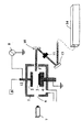
装置構成
図1に本発明で用いることができる容量結合方式を用いた平行平板方式のCVD装置の一例を示すが、本願発明はこの装置に限定されるものではない。なお、該図は説明のために過度に簡略化されている。また、この装置ではナノ粒子測定装置が備わっているが、生産装置ではこのような測定装置を装備する必要はないが、あればプラズマ反応、成膜反応をモニターしながら生産することもできる。
Apparatus Configuration FIG. 1 shows an example of a parallel plate type CVD apparatus using a capacitive coupling system that can be used in the present invention, but the present invention is not limited to this apparatus. Note that the drawing is excessively simplified for the sake of explanation. Further, although this apparatus is equipped with a nanoparticle measuring apparatus, the production apparatus does not need to be equipped with such a measuring apparatus, but can be produced while monitoring the plasma reaction and the film forming reaction.
反応器1の内部に、1対の導電性の平板電極、上部電極2と下部電極4を反応室内に平行に対向して置き、片側に例えば13.56 MHzのRF電力8を印加し、もう片側を電気的に接地する事により、この1対の電極間にプラズマを励起する。下部電極4は基板を支持する下部ステージの役割も果たし、基板3は下部ステージ4上に載置される。下部ステージ4には温度調整機構が付けられ、成膜中は、例えば約0℃〜約450℃(好ましくは約150℃〜約400℃)の所定の温度に一定に保たれる(基板温度もほど同じである)。材料ガス、例えばジメチルジメトキシシラン:Dimethyldimetoxysilane(DM-DMOS、Si(CH3)2(OCH3)2)、と不活性ガス、例えばAr、を混合し反応ガスとして用いる。これらのガスは流量制御装置9を通してそれぞれ所定の流量に制御され、これらが混合され反応ガスとして上部電極(シャワープレート)2の上部の導入口12に導入される。
Inside the
ナノ粒子のサイズ・密度の計測方法
凝集散乱法を適用し、ナノ粒子のサイズ・密度の計測を行うことができる。放電条件及びレーザーの入射条件の一例を以下に示すが、これに限られるものではない。
Measurement method of size and density of nanoparticles The size and density of nanoparticles can be measured by applying the aggregation scattering method. Examples of discharge conditions and laser incident conditions are shown below, but are not limited thereto.
<入射Arイオンレーザーの条件>
入射パワー: ~1W
レーザー径: 5mm(ICCDカメラ使用時), 0.5mm(PMT使用時)
Ar+レーザー(488nm、1W)14からレーザー光を照射し、ミラー13で反射後、グランレーザープリズム(Glan-Thompson Prism)11を介し光の偏光方向を揃え、ミラー10により、反応器1の壁に設けられた真空遮断のガラス(クオーツ製等)の窓5を通って反応器1内に照射される。レーザー光は反応器1中のナノ粒子生成領域を通って反応器1の対向する壁に設けられた窓6を経てICCDカメラ7で観測(あるいは電子倍増管PMT(Photomultiplier)で光検出)される。粒子間の熱的凝集現象をレーザー散乱法にて観測することで、微粒子のサイズをその場測定することができる。
<Conditions of incident Ar ion laser>
Incident power: ~ 1W
Laser diameter: 5mm (when using an ICCD camera), 0.5mm (when using a PMT)
Laser light is irradiated from an Ar + laser (488 nm, 1 W) 14, reflected by the
ナノ粒子のサイズ制御と放電時間
微粒子のサイズは、放電時間の制御により決めることができる。図2に微粒子サイズの放電時間依存性の一例を示す。この実験では、RF電力11.9W/cm2(13.56 MHz)、放電時間0.3秒、Ar 4000sccm、DMDMOS 20sccm、1Torr、基板温度250℃、電極サイズφ200mm、電極間距離20mm、放電領域内ガス流速(電極面に平行方向)1.0cm/秒の条件のもとで行われ、粒子間の熱的凝集現象をレーザー散乱法にて観測することで、微粒子のサイズをその場測定した。この図からも明らかなようにこの実施例においては、放電開始約0.1秒後には、1nm程度のナノ粒子が発生し、放電時間の経過とともにサイズが大きくなる。微粒子サイズが放電時間に対し線形的に成長し、2nm程度の微粒子を作成するには約0.15秒の放電時間を要することが分かる。放電時間の選択により、約1ナノメートルから約30ナノメートルの範囲で線形的にサイズの制御が可能である。なお、サイズが1ナノメートル付近でばらつきが大きいのはサイズとその場測定の信号強度が急激に小さくなり、S/N比が悪くなるためである。サイズが1/2になるとその場測定の信号強度は(1/2)6にまで低下する。これは測定の問題であり、TEM観測からも小さなサイズの領域でもサイズコントロールは精度よく実施できることを確認している。
Nanoparticle Size Control and Discharge Time The size of the fine particles can be determined by controlling the discharge time. FIG. 2 shows an example of the dependency of the particle size on the discharge time. In this experiment, RF power 11.9W / cm 2 (13.56 MHz), discharge time 0.3 seconds, Ar 4000sccm, DMDMOS 20sccm, 1Torr, substrate temperature 250 ° C, electrode size φ200mm, distance between electrodes 20mm, gas flow rate in the discharge region (electrode) The particle size was measured in situ by observing the thermal agglomeration phenomenon between particles by the laser scattering method under the condition of 1.0 cm / sec in the direction parallel to the surface. As is apparent from this figure, in this example, nanoparticles of about 1 nm are generated about 0.1 second after the start of discharge, and the size increases with the lapse of discharge time. It can be seen that the fine particle size grows linearly with respect to the discharge time, and it takes about 0.15 seconds of discharge time to produce fine particles of about 2 nm. Depending on the choice of discharge time, size can be linearly controlled in the range of about 1 nanometer to about 30 nanometers. The reason why the variation is large in the vicinity of 1 nanometer is that the size and the signal intensity of the in-situ measurement are drastically reduced and the S / N ratio is deteriorated. When the size is halved, the in-situ measurement signal strength drops to (1/2) 6 . This is a measurement problem, and it has been confirmed from TEM observation that size control can be performed accurately even in a small size region.
点線は、実験データの線形近似曲線で、サイズ成長率が約6.5nm/秒と与えられる。ここで、データをフィッテングする際に、初期サイズとしてDMDMOS分子のサイズを(0.93nm)とした。放電時間を約1 m秒から約1秒の範囲で制御する事によりnmオーダーのサイズに線形的に精度よく制御できる事がわかる。このように導電体粒子でないSi絶縁体粒子のプラズマCVDでの粒子生成現象については報告されていない。 The dotted line is a linear approximation curve of the experimental data, and the size growth rate is given as about 6.5 nm / second. Here, when fitting data, the size of the DMDMOS molecule was set to (0.93 nm) as an initial size. It can be seen that by controlling the discharge time in the range of about 1 msec to about 1 sec, the size can be controlled linearly and accurately to the size of nm order. Thus, there has been no report on the particle generation phenomenon in plasma CVD of Si insulator particles that are not conductor particles.
生成ナノ粒子の基板への輸送時間
ナノ粒子は、拡散による輸送とガス流により輸送され、一般的にはこの2つの効果が混在する。どちらの効果で主として輸送したいかにより装置構成や圧力が決まる。低圧力で電極間が狭い場合は、拡散での輸送が支配的となり、圧力が高い場合拡散速度より速いガス流でナノ粒子が輸送される。
Transport time of produced nanoparticles to substrate Nanoparticles are transported by diffusion and gas flow, and generally these two effects are mixed. Depending on which effect is desired to transport, the device configuration and pressure are determined. When the pressure is low and the distance between the electrodes is narrow, transport by diffusion is dominant, and when the pressure is high, the nanoparticles are transported by a gas flow faster than the diffusion rate.
拡散での輸送現象は、高周波電極周辺で生成されたナノ粒子が気体分子との衝突を介し拡散しつつ基板に輸送される。この拡散の速さを規定する拡散係数D(単位時間あたりの粒子の広がり面積)は以下の式で与えられる。 In the transport phenomenon due to diffusion, nanoparticles generated around the high-frequency electrode are transported to the substrate while diffusing through collision with gas molecules. The diffusion coefficient D (particle spreading area per unit time) that defines the speed of diffusion is given by the following equation.
輸送時間は、τd=L2/Dとして定義し、Lは輸送距離(電極間距離)である。輸送時間は微粒子サイズ及びガス圧に依存するが、ガス圧1Torr、質量約10-23kg、不活性ガスAr、ガス温度100℃、のもとで数ナノメートルの微粒子に対し概ね0.1〜1秒程度である。図3に拡散による輸送距離を1cmとした際の輸送に要する時間を示す(その他の条件は上記のナノ粒子のサイズ制御と放電時間の実験と同じである)。低ガス圧での小さい微粒子ほど拡散しやすいので輸送時間は短くなる。なお、この範囲は材料ガスの種類、不活性ガスの種類、ガス温度等にあまり影響されない。 The transport time is defined as τ d = L 2 / D, where L is the transport distance (distance between electrodes). Although the transport time depends on the particle size and gas pressure, it is approximately 0.1 to 1 second for particles of several nanometers under a gas pressure of 1 Torr, a mass of about 10-23 kg, an inert gas Ar, and a gas temperature of 100 ° C. Degree. FIG. 3 shows the time required for transport when the transport distance by diffusion is set to 1 cm (other conditions are the same as those in the above-mentioned experiment for controlling the size of nanoparticles and the discharge time). The smaller the fine particles at low gas pressure, the easier it is to diffuse, so the transport time is shorter. This range is not significantly affected by the type of material gas, the type of inert gas, the gas temperature, and the like.
電極間隔Lが20mmでは、拡散による輸送時間は約0.4秒、Lが10mmの場合は約0.1秒である。この輸送時間が経過すると電極間の粒子密度が十分に減少し、輸送時間が経過した後にRFをonにすればナノ粒子の生成が再び開始される。連続的な繰り返しで堆積膜厚を増加させる事ができる。 When the electrode interval L is 20 mm, the transport time by diffusion is about 0.4 seconds, and when L is 10 mm, it is about 0.1 seconds. When the transport time elapses, the particle density between the electrodes is sufficiently reduced, and when the RF is turned on after the transport time elapses, the generation of nanoparticles starts again. The deposited film thickness can be increased by continuous repetition.
また、ガス流で主に微粒子が輸送されている場合は、 In addition, when fine particles are mainly transported by gas flow,
τd:輸送時間(秒)
N:シャワープレートのガスノズルの個数
A:シャワーヘッドのガスノズルの断面積(cm2)
P:リアクターの圧力(Torr)
L:リアクターの電極間隔(cm)
式を展開する事により、
τ d : transport time (seconds)
N: Number of shower plate gas nozzles
A: Shower head gas nozzle cross section (cm 2 )
P: Reactor pressure (Torr)
L: Reactor electrode spacing (cm)
By expanding the expression,
輸送中での微粒子の凝集成長の抑止
緻密で一様なポーラス膜を作製する為には、輸送中での微粒子の凝集成長を抑止することが極めて重要なキーポイントになる。輸送途中において微粒子が凝集すると、綿状の塊ができ緻密で一様なポーラス膜の作製が困難になる。微粒子間の熱運動に起因する凝集成長の時間はτc=1/kcnpで与えられる。ここで、kc及びnpは凝集係数及び微粒子の密度で、凝集係数は以下の式で与えられる。
Inhibition of Aggregation Growth of Fine Particles During Transport In order to produce a dense and uniform porous film, it is an extremely important key point to inhibit the aggregation growth of fine particles during transportation. If the fine particles are aggregated during transportation, a cotton-like lump is formed, and it becomes difficult to produce a dense and uniform porous film. The time of aggregation growth due to the thermal motion between the fine particles is given by τ c = 1 / k c np . Here, k c and n p are the aggregation coefficient and fine particle density, and the aggregation coefficient is given by the following equation.
図4に微粒子の凝集時間を示す(その他の条件は上記のナノ粒子のサイズ制御と放電時間の実験と同じである)。微粒子密度1010cm-3でのナノ粒子に対し、凝集時間(τc)は概0.1〜0.3秒である。輸送中における微粒子の凝集成長を抑制するには、輸送時間を凝集時間より短くする(τd<τc)ようにすることが好ましい。すなわち、微粒子の発生量をある程度抑え輸送距離を短くすることが好ましい。
τd<τc
FIG. 4 shows the agglomeration time of the fine particles (other conditions are the same as those in the experiment on the size control of the nanoparticles and the discharge time). For nanoparticles with a fine particle density of 10 10 cm −3 , the aggregation time (τ c ) is approximately 0.1 to 0.3 seconds. In order to suppress the aggregation growth of fine particles during transportation, it is preferable to make the transportation time shorter than the aggregation time (τ d <τ c ). That is, it is preferable to reduce the amount of fine particles generated to some extent and shorten the transport distance.
τ d <τ c
輸送時間は、拡散効果とガス流の2つの効果で決まるが、拡散による輸送のみでのτdは一般に大きい(上記の例では0.1秒から1秒)ので上記関係式を満足するにはガス流により輸送速度を増大させることが好ましい。拡散による輸送を無視できる程度にガス流による輸送が支配的である輸送系では、ガス流の条件により輸送中での凝縮を制御する事ができる。凝縮成長時間τc= 0.1秒として、L=1cm, A=0.0079cm2 (φ0.5mm)、N=9000の場合、 The transport time is determined by the two effects of diffusion and gas flow. However, τ d of transport only by diffusion is generally large (0.1 to 1 second in the above example). It is preferable to increase the transport speed by the above. In a transport system in which transport by gas flow is dominant to such an extent that transport by diffusion is negligible, condensation during transport can be controlled by gas flow conditions. Condensation growth time τ c = 0.1 second, L = 1cm, A = 0.0079cm 2 (φ0.5mm), N = 9000,
膜特性
上記の方法により得られた膜の誘電率はある態様によれば2.0から2.5、更には2.1から2.4である。また、生成膜のモジュラスはある態様においては約1GPaから約4GPaである(キュア後の膜では約10%から約50%の改善する)。また、RIはある態様では1.1から1.4である。更に率はある態様では約30%から約85%、更に約40%から約75%、あるいは約50%から約70%である。なお、膜厚は用途により適宜調整することができ、特に限定されるものではないが、ある態様では約20nmから約2000nm、更に約50nmから約1000nm、あるいは約100nmから約500nmである。
Film Characteristics The film obtained by the above method has a dielectric constant of 2.0 to 2.5, and further 2.1 to 2.4, according to an embodiment. Also, the modulus of the resulting film is in some embodiments from about 1 GPa to about 4 GPa (improved from about 10% to about 50% for the cured film). Also, RI is 1.1 to 1.4 in some embodiments. Further, the rate is in some embodiments from about 30% to about 85%, further from about 40% to about 75%, or from about 50% to about 70%. The film thickness can be appropriately adjusted depending on the application, and is not particularly limited, but in a certain embodiment, it is about 20 nm to about 2000 nm, further about 50 nm to about 1000 nm, or about 100 nm to about 500 nm.
堆積膜実施例
Eagle-10(商標)(日本エー・エス・エム社製)を使い、下記の条件に基づき、ナノ粒子を生成、堆積させるサイクルを繰り返すことで膜厚400nmのSiOH系の低誘電率膜を形成した。
・ サセプタの温度 :250℃
・ 電極サイズ : φ 200mm
・ シャワープレートとサセプタとの間隔:20mm
・ ガス共通条件:Ar 4000sccm, DMDMOS 20 sccm,
放電領域内ガス流速(電極面に平行)1.0cm/秒 1Torr,
・ RF Power 13.56 MHz、2600 W(8.28W/cm2 )
・ RF on時間:0.15秒、 off時間:0.5秒
・ 成膜時間 : 70秒
Example of deposited film
Using Eagle-10 (trade name) (manufactured by Japan ASM Co., Ltd.), a SiOH-based low dielectric constant film with a film thickness of 400 nm is formed by repeating the cycle of generating and depositing nanoparticles based on the following conditions. did.
・ Temperature of susceptor: 250 ℃
・ Electrode size: φ200mm
・ Distance between shower plate and susceptor: 20mm
・ Common gas conditions: Ar 4000sccm, DMDMOS 20 sccm,
Gas flow rate in the discharge area (parallel to the electrode surface) 1.0cm / sec 1Torr,
・ RF Power 13.56 MHz, 2600 W (8.28 W / cm 2 )
・ RF on time: 0.15 seconds, off time: 0.5 seconds ・ Deposition time: 70 seconds
得られた膜の特性は以下の通りであった。
・ 膜厚: 400nm
・ RI(n) : 1.29
・ 空孔率(%) : 65%
・ 誘電率 : k=2.2
以上説明したように、本発明の少なくとも一実施態様によれば、プラズマCVD方式による低誘電率膜の成膜が可能となる。この低誘電率膜を、次世代の高集積半導体素子の絶縁膜として使用する事により、配線間容量による遅延を下げ半導体素子の動作速度を大幅に上げる事が可能となる。
The characteristics of the obtained film were as follows.
・ Film thickness: 400nm
・ RI (n): 1.29
・ Porosity (%): 65%
・ Dielectric constant: k = 2.2
As described above, according to at least one embodiment of the present invention, it is possible to form a low dielectric constant film by a plasma CVD method. By using this low dielectric constant film as an insulating film for the next-generation highly integrated semiconductor device, it is possible to reduce the delay due to the capacitance between wirings and to greatly increase the operation speed of the semiconductor device.
本発明は以下の実施態様に限定はされないが、それらを含むものである。
1)容量結合方式のCVD装置による成膜をおいて次の条件下で実施する。
・ Siを少なくとも含み、その他 C, O, Hで構成される、有機Siガス(一般式SiαHβOγCλ :α、β、γ、λは任意の整数)を材料ガスとして用いる。
・ 不活性ガスにより有機Siガスの流量比を約10%以下に希釈する。
・ 反応圧力を約0.1 Torr から約 10 Torrの圧力領域とする。
・ nmオーダーの微粒子を気相中に生成し、それを堆積する事により低誘電率の絶縁膜を形成する。
The present invention is not limited to the following embodiments, but includes them.
1) The film is formed by the capacitive coupling type CVD apparatus under the following conditions.
An organic Si gas (general formula Si α H β O γ C λ : α, β, γ, λ is an arbitrary integer) containing at least Si and composed of C, O, and H is used as a material gas.
・ Use an inert gas to dilute the flow ratio of organic Si gas to about 10% or less.
・ Set the reaction pressure in the pressure range from about 0.1 Torr to about 10 Torr.
・ Generate nanometer-order fine particles in the gas phase and deposit them to form an insulating film with a low dielectric constant.
2)該有機シリコンガスはSiαOα−1R2α−β+2(OCnH2n+1)β:ここでαは1〜3の整数、βは0, 1,2 ,3または4、nは1〜3の整数、RはSiに結合するC1-6 炭化水素の一般式で表される。 2) The organic silicon gas is Si α O α-1 R 2α-β + 2 (OC n H 2n + 1 ) β : where α is an integer of 1 to 3, β is 0, 1, 2, 3 or 4, n Is an integer of 1 to 3, and R is represented by a general formula of C 1-6 hydrocarbon bonded to Si.
3)該有機シリコンガスは、SiR4−α(OCnH2n+1)α :ここでαは0, 1,2 ,3または4、nは1〜3の整数、RはSiに結合するC1-6 炭化水素である。 3) The organic silicon gas is SiR 4-α (OC n H 2n + 1 ) α : where α is 0, 1, 2, 3 or 4, n is an integer of 1 to 3, and R is bonded to Si C 1-6 hydrocarbon.
4)該有機シリコンガスは、Si2OR6−α(OCnH2n+1)α :ここでαは0, 1,2 ,3または4、nは1〜3の整数、RはSiに結合するC1-6 炭化水素である。 4) The organic silicon gas is Si 2 OR 6-α (OC n H 2n + 1 ) α : where α is 0, 1, 2, 3 or 4, n is an integer of 1 to 3, and R is Si Combined C 1-6 hydrocarbons.
5)該有機シリコンガスは、SiHβR4−α(OCnH2n+1)α−β :ここでαは0, 1,2 ,3または4、βは0, 1,2 ,3または4、 nは1または2、RはSiに結合するC1-6炭化水素である。 5) The organic silicon gas is SiH β R 4-α (OC n H 2n + 1 ) α-β : where α is 0, 1, 2, 3 or 4, and β is 0, 1, 2, 3 or 4, n is 1 or 2, and R is a C 1-6 hydrocarbon bonded to Si.
6)1m秒〜1 秒のRFの印加時間でナノ粒子を形成し、粒子の輸送時間の間RFをoffにする堆積工程を組み合わせ、膜を堆積する。1回または複数回の連続サイクルも含まれる。 6) A nanoparticle is formed with an RF application time of 1 msec to 1 sec, and a film is deposited by combining a deposition process in which RF is turned off during the particle transport time. One or more successive cycles are also included.
7)有機Siガスとて、DMDMOS:Si(CH3)2(OCH3)2を材料ガスとして、不活性ガスとしてArを用いる。 7) As the organic Si gas, DMDMOS: Si (CH 3 ) 2 (OCH 3 ) 2 is used as a material gas, and Ar is used as an inert gas.
8)RF電力として13.56 MHz, 27 MHz, 60 MHzのRF電力を用いる。 8) Use RF power of 13.56 MHz, 27 MHz, 60 MHz as RF power.
9)100 MHz以上のVHF帯の高周波電力を用いる。 9) Use high-frequency power in the VHF band of 100 MHz or higher.
10)VHF帯の高周波電力を用いる場合、スポークアンテナ電極を用いる。 10) When using high frequency power in the VHF band, use a spoke antenna electrode.
11)基板温度を0℃〜450℃の範囲で成膜する。 11) The film is formed at a substrate temperature ranging from 0 ° C to 450 ° C.
12)基板温度を150℃〜400℃の範囲で成膜する。 12) Film formation is performed at a substrate temperature in the range of 150.degree.
13)有機Siガスとて、 Si(CH3)4 , Si(CH3)3(OCH3), Si(CH3)2(OCH3)2, Si(CH3)(OCH3)3, Si(OCH3)4, Si(CH3)3(OC2H5), Si(CH3)2(OC2H5)2, Si(CH3)(OC2H5)3, Si(OC2H5)4, SiH(CH3)3, SiH2(CH3)2, SiH3(CH3)の一つまたは、この複数の組み合わせを用いる。 13) Organic Si gas, Si (CH 3 ) 4 , Si (CH 3 ) 3 (OCH 3 ), Si (CH 3 ) 2 (OCH 3 ) 2 , Si (CH 3 ) (OCH 3 ) 3 , Si (OCH 3 ) 4 , Si (CH 3 ) 3 (OC 2 H 5 ), Si (CH 3 ) 2 (OC 2 H 5 ) 2 , Si (CH 3 ) (OC 2 H 5 ) 3 , Si (OC 2 One of H 5 ) 4 , SiH (CH 3 ) 3 , SiH 2 (CH 3 ) 2 , SiH 3 (CH 3 ) or a combination of these is used.
14)不活性ガスとして ArまたはHe, Ne, Kr, Xe, N2のひとつまたはその組み合わせを用いる。 14) Ar or He, Ne, Kr, Xe, or N 2 or a combination thereof is used as the inert gas.
15)O2、CO, CO2, N2Oなどの酸化性ガスを添加し、生成膜のカーボン濃度を調整する。 15) Add oxidizing gas such as O 2 , CO, CO 2 , N 2 O and adjust the carbon concentration of the resulting film.
16)反応空間でのナノ粒子の輸送時間を凝集時間より短くする条件での成膜を行う。 16) Film formation is performed under the condition that the nanoparticle transport time in the reaction space is shorter than the aggregation time.
17)膜の機械的強度を改善するため、成膜後の膜をUVまたはEBと組み合わせた熱処理でキュアを行う。 17) In order to improve the mechanical strength of the film, the film after film formation is cured by heat treatment combined with UV or EB.
18)膜の機械的強度を改善するため、成膜後の膜をプラズマ処理、UVまたはEBと組み合わせた熱処理でキュアを行う。 18) In order to improve the mechanical strength of the film, the film after film formation is cured by plasma treatment and heat treatment combined with UV or EB.
19)電子式RF整合機を用いる。 19) Use an electronic RF matching machine.
20)微粒子膜形成後に有機シリコンガス雰囲気に放置し、有機シリコン分子を微粒子膜に付着させる工程とキュアを行い膜強度の改善を行う。 20) After forming the fine particle film, the film is left in an organic silicon gas atmosphere, and the film strength is improved by performing a step of curing organic silicon molecules on the fine particle film and curing.
21)微粒子膜形成後に、H2Oガス雰囲気に放置する工程と有機シリコンガス雰囲気に放置する工程を短数回または複数回繰り返し、膜強度の改善を行う。 21) After forming the fine particle film, the step of leaving in the H 2 O gas atmosphere and the step of leaving in the organic silicon gas atmosphere are repeated a few times or a plurality of times to improve the film strength.
本発明の実施態様の説明では図面を参照するが、本発明はそれらの図面及び実施態様に限定されるものではない。
Claims (54)
該有機Siガスから気相中に生成する微粒子のサイズを該反応器内におけるプラズマ放電時間の関数として、nmオーダーに調整する工程、及び
生成した該微粒子を該反応器内に載置された基板上に堆積する工程、
を包含する、低誘電率膜を形成する方法。 Introducing a reaction gas composed of an organic Si gas and an inert gas into a reactor of a capacitively coupled CVD apparatus;
Adjusting the size of the fine particles produced in the gas phase from the organic Si gas as a function of the plasma discharge time in the reactor to the order of nm, and the substrate on which the produced fine particles are placed in the reactor Depositing on the top,
Forming a low dielectric constant film.
N:シャワープレートのガスノズルの個数
A:シャワープレートのガスノズルの断面積(cm2)
P:反応器内の圧力(Torr)
L:電極間隔(cm) The reaction gas is introduced through a gas nozzle of a shower plate provided in the reactor, the plasma discharge is performed between the upper and lower electrodes, and the substrate is placed on the lower electrode. 9. The method of claim 8, wherein the method is adjusted to satisfy the relational expression.
N: Number of shower plate gas nozzles
A: Shower plate gas nozzle cross section (cm 2 )
P: Reactor pressure (Torr)
L: Electrode spacing (cm)
反応ガス流量を次の関係式を満足するように調整する工程、
N:シャワープレートのガスノズルの個数
A:シャワープレートのガスノズルの断面積(cm2)
P:反応器内の圧力(Torr)
L:電極間隔(cm)
該有機Siガスから気相中に生成する微粒子のサイズを該反応器内におけるプラズマ放電時間の関数として、約10nm以下に調整する工程、及び
プラズマ放電を中止し生成した該微粒子を該反応器内に載置された基板上に堆積する工程、
を包含する、低誘電率膜を形成する方法。 Introducing a reaction gas composed of an organic Si gas and an inert gas into the reactor through a gas nozzle of a shower plate provided in the reactor;
Adjusting the reaction gas flow rate so as to satisfy the following relational expression:
N: Number of shower plate gas nozzles
A: Shower plate gas nozzle cross section (cm 2 )
P: Reactor pressure (Torr)
L: Electrode spacing (cm)
Adjusting the size of the fine particles produced in the gas phase from the organic Si gas to about 10 nm or less as a function of the plasma discharge time in the reactor, and stopping the plasma discharge to produce the fine particles produced in the reactor. Depositing on a substrate placed on
Forming a low dielectric constant film.
(B)プラズマ放電を実施し該有機Siガスから微粒子を形成する工程、及び
(C)該微粒子が形成されている約100m秒から約2秒の間に該微粒子を該反応器内に載置された基板上へ堆積させる工程、
を包含する、低誘電率膜を形成する方法。 (A) introducing a reaction gas composed of an organic Si gas and an inert gas into the reactor;
(B) performing plasma discharge to form fine particles from the organic Si gas; and (C) placing the fine particles in the reactor during about 100 milliseconds to about 2 seconds when the fine particles are formed. Depositing on a fabricated substrate;
Forming a low dielectric constant film.
(B)該有機Siガスからナノ粒子が形成される時間(T1)、形成されたナノ粒子が該反応器内に載置された基板上まで輸送される時間(T2)、ナノ粒子同士が輸送中に凝集成長を起こす時間(T3)を、プラズマ放電時間とガス流量の関数として制御し、ナノ粒子を該基板上に堆積する工程、
を包含する、低誘電率膜を形成する方法。 (A) introducing a reaction gas composed of an organic Si gas and an inert gas into the reactor, and performing plasma discharge to form nanoparticles from the organic Si gas; and (B) nanoparticles from the organic Si gas. Is formed (T1), the formed nanoparticles are transported to the substrate placed in the reactor (T2), and the nanoparticles are agglomerated during transportation (T3) Controlling as a function of plasma discharge time and gas flow rate, and depositing nanoparticles on the substrate;
Forming a low dielectric constant film.
(B)該有機Siガスからナノ粒子が形成される時間(T1)、形成されたナノ粒子が該反応器内に載置された基板上まで輸送される時間(T2)、ナノ粒子同士が輸送中に凝集成長を起こす時間(T3)を制御パラメータとし、該基板上へのナノ粒子の堆積を制御する工程、
を包含する、低誘電率膜を形成する方法。 (A) introducing a reaction gas composed of an organic Si gas and an inert gas into the reactor, and performing plasma discharge to form nanoparticles from the organic Si gas; and (B) nanoparticles from the organic Si gas. Is formed (T1), the formed nanoparticles are transported to the substrate placed in the reactor (T2), and the nanoparticles are agglomerated during transportation (T3) Controlling the deposition of nanoparticles on the substrate,
Forming a low dielectric constant film.
Applications Claiming Priority (1)
| Application Number | Priority Date | Filing Date | Title |
|---|---|---|---|
| US10/990,562 US20060105583A1 (en) | 2004-11-17 | 2004-11-17 | Formation technology of nano-particle films having low dielectric constant |
Publications (2)
| Publication Number | Publication Date |
|---|---|
| JP2006148100A true JP2006148100A (en) | 2006-06-08 |
| JP2006148100A5 JP2006148100A5 (en) | 2008-12-25 |
Family
ID=36386956
Family Applications (1)
| Application Number | Title | Priority Date | Filing Date |
|---|---|---|---|
| JP2005329871A Withdrawn JP2006148100A (en) | 2004-11-17 | 2005-11-15 | Formation technology for low-dielectric-constant nanoparticle film |
Country Status (2)
| Country | Link |
|---|---|
| US (1) | US20060105583A1 (en) |
| JP (1) | JP2006148100A (en) |
Cited By (2)
| Publication number | Priority date | Publication date | Assignee | Title |
|---|---|---|---|---|
| JP2008042208A (en) * | 2006-08-08 | 2008-02-21 | Asm Japan Kk | Method for forming silicon carbide film containing oxygen |
| JP2012502181A (en) * | 2008-09-03 | 2012-01-26 | ダウ コーニング コーポレーション | Low pressure radio frequency pulsed plasma reactor for the production of nanoparticles |
Families Citing this family (2)
| Publication number | Priority date | Publication date | Assignee | Title |
|---|---|---|---|---|
| JP4628900B2 (en) * | 2005-08-24 | 2011-02-09 | 株式会社日立ハイテクノロジーズ | Plasma processing equipment |
| JP5616737B2 (en) * | 2009-11-20 | 2014-10-29 | 株式会社日立国際電気 | Semiconductor device manufacturing method, substrate processing method, and substrate processing apparatus |
Family Cites Families (7)
| Publication number | Priority date | Publication date | Assignee | Title |
|---|---|---|---|---|
| US5763429A (en) * | 1993-09-10 | 1998-06-09 | Bone Care International, Inc. | Method of treating prostatic diseases using active vitamin D analogues |
| US6245690B1 (en) * | 1998-11-04 | 2001-06-12 | Applied Materials, Inc. | Method of improving moisture resistance of low dielectric constant films |
| KR100311234B1 (en) * | 1999-01-18 | 2001-11-02 | 학교법인 인하학원 | Enhanced inductively coupled plasma reactor |
| TW507256B (en) * | 2000-03-13 | 2002-10-21 | Mitsubishi Heavy Ind Ltd | Discharge plasma generating method, discharge plasma generating apparatus, semiconductor device fabrication method, and semiconductor device fabrication apparatus |
| US6602800B2 (en) * | 2001-05-09 | 2003-08-05 | Asm Japan K.K. | Apparatus for forming thin film on semiconductor substrate by plasma reaction |
| US6667577B2 (en) * | 2001-12-18 | 2003-12-23 | Applied Materials, Inc | Plasma reactor with spoke antenna having a VHF mode with the spokes in phase |
| US20030211244A1 (en) * | 2002-04-11 | 2003-11-13 | Applied Materials, Inc. | Reacting an organosilicon compound with an oxidizing gas to form an ultra low k dielectric |
-
2004
- 2004-11-17 US US10/990,562 patent/US20060105583A1/en not_active Abandoned
-
2005
- 2005-11-15 JP JP2005329871A patent/JP2006148100A/en not_active Withdrawn
Cited By (2)
| Publication number | Priority date | Publication date | Assignee | Title |
|---|---|---|---|---|
| JP2008042208A (en) * | 2006-08-08 | 2008-02-21 | Asm Japan Kk | Method for forming silicon carbide film containing oxygen |
| JP2012502181A (en) * | 2008-09-03 | 2012-01-26 | ダウ コーニング コーポレーション | Low pressure radio frequency pulsed plasma reactor for the production of nanoparticles |
Also Published As
| Publication number | Publication date |
|---|---|
| US20060105583A1 (en) | 2006-05-18 |
Similar Documents
| Publication | Publication Date | Title |
|---|---|---|
| US20060269690A1 (en) | Formation technology for nanoparticle films having low dielectric constant | |
| US6737366B2 (en) | Method of forming low dielectric constant insulation film for semiconductor device | |
| US9362107B2 (en) | Flowable low-k dielectric gapfill treatment | |
| KR100933374B1 (en) | Method for film formation of porous membrane and computer readable recording medium | |
| JP5269093B2 (en) | Silicon nitride film with low wet etching rate | |
| US9018108B2 (en) | Low shrinkage dielectric films | |
| US6830007B2 (en) | Apparatus and method for forming low dielectric constant film | |
| WO2004107825A9 (en) | Plasma source and plasma processing apparatus | |
| TWI380351B (en) | Plasma cvd apparatus and thin film forming method as well as semiconductor device | |
| WO2009111395A2 (en) | Method for depositing an amorphous carbon film with improved density and step coverage | |
| JP4743229B2 (en) | Method for forming semiconductor device using neutral particles | |
| KR20070057284A (en) | Process for film production and semiconductor device utilizing film produced by the process | |
| JP2006148100A (en) | Formation technology for low-dielectric-constant nanoparticle film | |
| JP5084426B2 (en) | Method for forming silicon nitride film | |
| EP2045357B1 (en) | Method of forming silicon nitride films | |
| KR20090006769A (en) | Method of forming porous film and computer-readable recording medium | |
| JP4180393B2 (en) | Method for forming low dielectric constant interlayer insulating film | |
| EP1256978A2 (en) | Method of forming low dielectric constant insulation film for semiconductor device | |
| JP3197008B2 (en) | Silicon polymer insulating film on semiconductor substrate and method for forming the film | |
| TW200538578A (en) | Microcontamination abatement in semiconductor processing | |
| TWI807230B (en) | Initiation modulation for plasma deposition | |
| JP2004356558A (en) | Apparatus and method for coating | |
| WO2006075578A1 (en) | Film forming material and method of film forming |
Legal Events
| Date | Code | Title | Description |
|---|---|---|---|
| RD04 | Notification of resignation of power of attorney |
Free format text: JAPANESE INTERMEDIATE CODE: A7424 Effective date: 20080331 |
|
| A521 | Request for written amendment filed |
Free format text: JAPANESE INTERMEDIATE CODE: A523 Effective date: 20081111 |
|
| A621 | Written request for application examination |
Free format text: JAPANESE INTERMEDIATE CODE: A621 Effective date: 20081111 |
|
| A761 | Written withdrawal of application |
Free format text: JAPANESE INTERMEDIATE CODE: A761 Effective date: 20090701 |