JP2006147367A - Pulse generation circuit, discharge lamp lighting device and lighting system - Google Patents
Pulse generation circuit, discharge lamp lighting device and lighting system Download PDFInfo
- Publication number
- JP2006147367A JP2006147367A JP2004336430A JP2004336430A JP2006147367A JP 2006147367 A JP2006147367 A JP 2006147367A JP 2004336430 A JP2004336430 A JP 2004336430A JP 2004336430 A JP2004336430 A JP 2004336430A JP 2006147367 A JP2006147367 A JP 2006147367A
- Authority
- JP
- Japan
- Prior art keywords
- resistor
- voltage
- capacitor
- thyristor
- discharge lamp
- Prior art date
- Legal status (The legal status is an assumption and is not a legal conclusion. Google has not performed a legal analysis and makes no representation as to the accuracy of the status listed.)
- Withdrawn
Links
Images


Classifications
-
- Y—GENERAL TAGGING OF NEW TECHNOLOGICAL DEVELOPMENTS; GENERAL TAGGING OF CROSS-SECTIONAL TECHNOLOGIES SPANNING OVER SEVERAL SECTIONS OF THE IPC; TECHNICAL SUBJECTS COVERED BY FORMER USPC CROSS-REFERENCE ART COLLECTIONS [XRACs] AND DIGESTS
- Y02—TECHNOLOGIES OR APPLICATIONS FOR MITIGATION OR ADAPTATION AGAINST CLIMATE CHANGE
- Y02B—CLIMATE CHANGE MITIGATION TECHNOLOGIES RELATED TO BUILDINGS, e.g. HOUSING, HOUSE APPLIANCES OR RELATED END-USER APPLICATIONS
- Y02B20/00—Energy efficient lighting technologies, e.g. halogen lamps or gas discharge lamps
Abstract
Description
本発明は、高輝度放電ランプ(以下、HIDランプ)を始動点灯させるパルス発生回路、放電灯点灯装置及び照明装置に関する。 The present invention relates to a pulse generation circuit, a discharge lamp lighting device, and an illumination device for starting and lighting a high-intensity discharge lamp (hereinafter, HID lamp).
従来からHIDランプを始動点灯させるには、高圧パルス発生手段としてイグナイタが用いられている。イグナイタは、コンデンサと、パルストランスと、スイッチング素子で構成される。 Conventionally, an igniter is used as a high-pressure pulse generating means for starting and lighting an HID lamp. The igniter includes a capacitor, a pulse transformer, and a switching element.
イグナイタのスイッチング素子としては、トライアック、サイリスタのような大容量のスイッチング素子を使用するが、このような素子は、外部信号によりオフできず、素子に流れる電流が一定の値(保持電流)以下になるとオフする。 As the igniter switching element, a large-capacity switching element such as a triac or thyristor is used. However, such an element cannot be turned off by an external signal, and the current flowing through the element falls below a certain value (holding current). Turn off.
HIDランプの放電灯点灯装置では、コンデンサに蓄えられたエネルギーをサイリスタをオンすることによりパルストランスの1次巻線に印加することで、パルストランスの2次巻線に略巻数比分の電圧が発生し、ランプに印加されてランプが始動できるようになる。オンした後にはコンデンサとパルストランスの1次巻線による振動電圧(共振電圧)によりサイリスタに逆電圧(振動電圧の負側の電圧)が印加されて、サイリスタはターンオフする。その際のコンデンサヘのエネルギー蓄積方法は簡単な方法として、電源から抵抗を介して電流を供給する方法がある。 In a discharge lamp lighting device for an HID lamp, by applying the energy stored in the capacitor to the primary winding of the pulse transformer by turning on the thyristor, a voltage corresponding to an approximate turn ratio is generated in the secondary winding of the pulse transformer. The lamp can be started by being applied to the lamp. After turning on, a reverse voltage (voltage on the negative side of the oscillating voltage) is applied to the thyristor by an oscillating voltage (resonant voltage) by the primary winding of the capacitor and the pulse transformer, and the thyristor is turned off. As a simple method for storing energy in the capacitor at that time, there is a method of supplying a current from a power source through a resistor.
しかし、ランプ始動時にはパルストランスの2次巻線に電流が流れ始めるためその1次巻線から見たインダクタンスは低くなる結果、共振が起こりにくくなり、サイリスタに印加される逆電圧の時間が短くなるために、サイリスタがオフ出来ない場合がある。さらに、サイリスタはその特性上、高温になるほどターンオフしにくくなる。その結果、サイリスタがオフできずにオンし続けると、電源を供給するための抵抗が加熱して部品としての劣化を招くと共に、無駄な電力消費が発生する。 However, since the current starts to flow in the secondary winding of the pulse transformer at the time of starting the lamp, the inductance seen from the primary winding becomes low. As a result, resonance hardly occurs and the time of the reverse voltage applied to the thyristor is shortened. Therefore, the thyristor may not be turned off. Furthermore, thyristors are less likely to turn off at higher temperatures due to their characteristics. As a result, if the thyristor cannot be turned off and continues to be turned on, a resistor for supplying power is heated to cause deterioration as a component, and wasteful power consumption occurs.
従来の高圧放電灯点灯装置としては、イグナイタのサイリスタをオフさせるために、サイリスタヘの電流を分流するバイパス回路を用意し、サイリスタをオンしてから、あらかじめ定められた時間経過後に、一定時間だけ、バイパス回路を駆動(オン)することで、充電電流を保持電流以下にしてサイリスタをオフできるようにしたものがある(例えば、特許文献1参照)。
上記のように、ランプ始動後においてもサイリスタがオフすることなく電流が流れるために、電源を供給するための抵抗が加熱して部品としての劣化を招くと共に、無駄な電力消費が発生するという問題があった。 As described above, since the current flows without turning off the thyristor even after the lamp is started, the resistance for supplying power is heated to cause deterioration as a component, and wasteful power consumption occurs. was there.
そこで、本発明は上記の問題に鑑み、ランプ始動後にサイリスタを確実にオフでき、電源を供給するための抵抗が加熱して劣化を招くのを防ぐと共に、無駄な電力消費が発生するのを防止できるパルス発生回路、放電灯点灯装置及び照明装置を提供することを目的とするものである。 Therefore, in view of the above problems, the present invention can surely turn off the thyristor after starting the lamp, prevent the resistor for supplying power from being heated and causing deterioration, and prevent unnecessary power consumption from occurring. An object of the present invention is to provide a pulse generation circuit, a discharge lamp lighting device, and a lighting device that can be used.
請求項1記載の発明によるパルス発生回路は、放電ランプに2次巻線が直列に接続され、1次巻線に発生するパルスを前記2次巻線に昇圧して出力するトランスと; 放電ランプと前記トランスの2次巻線の直列回路と並列に接続される第1のコンデンサと;前記トランスの1次巻線と閉回路を構成する第2のコンデンサとサイリスタと;前記第2のコンデンサに電源を供給する抵抗と;前記サイリスタのオンタイミングを制御する制御手段と;前記抵抗に電圧が印加されている時間を計測するタイマー手段と;前記抵抗に直列接続され、前記タイマー手段が所定時間以上前記抵抗に電圧が印加されていることを検出したときに、前記電源から前記第2のコンデンサヘの充電電流を遮断する遮断手段と;を具備したものである。 A pulse generation circuit according to a first aspect of the present invention includes a transformer in which a secondary winding is connected in series to a discharge lamp, and a pulse generated in the primary winding is boosted and output to the secondary winding; And a first capacitor connected in parallel with the series circuit of the secondary winding of the transformer; a second capacitor and a thyristor constituting a closed circuit with the primary winding of the transformer; and the second capacitor A resistor for supplying power; a control means for controlling the on-timing of the thyristor; a timer means for measuring a time during which a voltage is applied to the resistance; and connected in series to the resistor, and the timer means is not less than a predetermined time. And a blocking means for cutting off a charging current from the power source to the second capacitor when it is detected that a voltage is applied to the resistor.
この発明において、放電ランプとしては、水銀ランプ、メタルハライドランプ、高圧ナトリウムランプ、キセノンランプを含むHIDランプを含む。以上の事項は、以下の発明でも同様である。 In the present invention, discharge lamps include HID lamps including mercury lamps, metal halide lamps, high pressure sodium lamps, and xenon lamps. The above matters also apply to the following inventions.
この発明によれば、サイリスタがオフできずにオンし続けた場合には、、抵抗に連続した一定の電流が流れるので、抵抗に発生する電圧を検知し、この電圧検出に基づいて抵抗からサイリスタヘ流れる電流を遮断してサイリスタをオフし、再び高圧パルスの発生を可能とする。 According to the present invention, when the thyristor continues to be turned on without being turned off, a constant current flowing through the resistor flows. Therefore, the voltage generated in the resistor is detected, and the resistor detects the voltage from the resistor to the thyristor. The current that flows is cut off, the thyristor is turned off, and a high-pressure pulse can be generated again.
請求項2記載の発明によるパルス発生回路は、放電ランプに2次巻線が直列に接続され、1次巻線に発生するパルスを前記2次巻線に昇圧して出力するトランスと;放電ランプと前記トランスの2次巻線の直列回路と並列に接続される第1のコンデンサと;前記トランスの1次巻線と閉回路を構成する第2のコンデンサとサイリスタと;前記第2のコンデンサに電源を供給する抵抗と;前記サイリスタのオンタイミングを制御する制御手段と; 前記抵抗の温度を検出する温度検出部を備え、且つ前記抵抗に直列接続され、前記抵抗の温度が所定値以上であることを検出したときに、前記電源から前記第2のコンデンサヘの充電電流を遮断する温度反応型スイッチ素子と;を具備したものである。 According to a second aspect of the present invention, there is provided a pulse generation circuit comprising: a transformer having a secondary winding connected in series to a discharge lamp; a transformer for boosting and outputting a pulse generated in the primary winding to the secondary winding; And a first capacitor connected in parallel with the series circuit of the secondary winding of the transformer; a second capacitor and a thyristor constituting a closed circuit with the primary winding of the transformer; and the second capacitor A resistor for supplying power; a control means for controlling on-timing of the thyristor; a temperature detection unit for detecting a temperature of the resistor, and connected in series to the resistor, wherein the temperature of the resistor is equal to or higher than a predetermined value And a temperature-responsive switch element that cuts off a charging current from the power source to the second capacitor when it is detected.
この発明によれば、サイリスタがオフできずにオンし続けた場合には、抵抗に連続した一定の電流が流れるので、抵抗に発生する温度を検知し、この温度検出に基づいて抵抗からサイリスタヘ流れる電流を遮断してサイリスタをオフし、再び高圧パルスの発生を可能とする。 According to the present invention, when the thyristor continues to be turned on without being turned off, a constant current flowing through the resistor flows. Therefore, the temperature generated in the resistor is detected, and based on this temperature detection, the current flows from the resistor to the thyristor. The current is cut off, the thyristor is turned off, and a high voltage pulse can be generated again.
請求項3記載の発明によるパルス発生回路は、請求項2に記載のパルス発生回路において、前記温度反応型スイッチ素子は、サーマルプロテクタであることを特徴とする。 A pulse generation circuit according to a third aspect of the present invention is the pulse generation circuit according to the second aspect, wherein the temperature-responsive switch element is a thermal protector.
請求項4記載の発明による放電灯点灯装置は、交流電源の出力から直流電圧を生成する直流電圧源と;前記直流電圧源に接続されて、交流電力を生成して放電ランプの点灯を維持させるインバータ回路と;前記インバータ回路に組み込まれて、昇圧パルスにて前記放電ランプを始動させる請求項1乃至3のいずか1つに記載のパルス発生回路と;を具備したものである。
A discharge lamp lighting device according to a fourth aspect of the present invention is a DC voltage source that generates a DC voltage from an output of an AC power source; and is connected to the DC voltage source to generate AC power and maintain the lighting of the discharge lamp. An inverter circuit; and a pulse generation circuit according to any one of
この発明の放電灯点灯装置によれば、ランプ始動後にサイリスタを確実にオフでき、電源を供給するための抵抗が加熱して劣化を招くのを防ぐと共に、無駄な電力消費が発生するのを防止できる。 According to the discharge lamp lighting device of the present invention, the thyristor can be surely turned off after the lamp is started, the resistance for supplying power is prevented from being heated and causing deterioration, and unnecessary power consumption is prevented from occurring. it can.
請求項5記載の発明による照明装置は、請求項4に記載の放電灯点灯装置と;放電ランプとしてのHIDランプと;前記HIDランプを保持する器具本体と;を具備したものである。 According to a fifth aspect of the present invention, there is provided an illumination device comprising: the discharge lamp lighting device according to the fourth aspect; an HID lamp as a discharge lamp; and an appliance main body for holding the HID lamp.
この発明の照明装置によれば、ランプ始動後にサイリスタを確実にオフでき、電源を供給するための抵抗が加熱して劣化を招くのを防ぐと共に、無駄な電力消費が発生するのを防止できる。 According to the lighting device of the present invention, the thyristor can be reliably turned off after the lamp is started, the resistance for supplying power can be prevented from being heated and causing deterioration, and wasteful power consumption can be prevented from occurring.
本発明によれば、サイリスタが確実にオフできるので、パルスが停止してしまうことがなく、ランプを確実に始動できる。また、ランプ始動後にイグナイタの抵抗による無駄な消費電力を抑制することができる。 According to the present invention, since the thyristor can be reliably turned off, the pulse is not stopped and the lamp can be reliably started. In addition, useless power consumption due to the resistance of the igniter after starting the lamp can be suppressed.
発明の実施の形態について図面を参照して説明する。 Embodiments of the invention will be described with reference to the drawings.
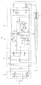
図1は本発明の実施例1の放電灯点灯装置を示す回路図である。
図1において、低周波(例えば50Hz)の電源である商用交流電源1の出力端の両端に、全波整流ダイオードブリッジで構成される整流回路2が接続されている。
1 is a circuit diagram showing a discharge lamp lighting device according to a first embodiment of the present invention.
In FIG. 1, a
整流回路2の全波整流出力端間には、後述の高周波スイッチング用のスイッチング素子であるFETQ1の高周波スイッチングに伴う高周波成分通流用フィルタとしてコンデンサC5が接続され、さらにその後段には、整流回路2の出力電圧を昇圧しかつ安定した直流電圧として高力率で出力する昇圧チョッパ回路3が接続されている。
A capacitor C5 is connected between the full-wave rectification output terminals of the
昇圧チョッパ回路3は、制御回路7の制御のもとで、整流回路2からの全波整流出力を入力して振幅一定な安定化した直流電圧を高力率で生成するアクティブフィルタ回路或いは直流電源と言える。なお、整流回路2の全波整流出力端間には、昇圧チョッパ回路3の一部の機能、即ち入力交流電流と入力交流電源電圧の位相を合わせる入力力率改善機能のみを備えたアクティブフィルタ回路が接続されていてもよい。
The step-up chopper circuit 3 receives the full-wave rectified output from the
昇圧チョッパ回路3は、整流回路2の一方の出力端(図では+電圧出力端)に一端部が接続されたコイルL1と、このコイルL1の他端部と整流回路2のもう一方の出力端(図では−電圧出力端)の間にドレイン・ソースが接続された高周波スイッチング素子としてのFETQ1と、コイルL1とFETQ1間の接続点にアノードが接続された転流ダイオードD5と、この転流ダイオードD5のカソードと整流回路2の−電圧出力端との間に接続された第1,第2の平滑コンデンサC2,C3の直列回路と、を備えている。
The step-up chopper circuit 3 includes a coil L1 having one end connected to one output end (+ voltage output end in the figure) of the
制御回路7は、昇圧チョッパ回路3の第1,第2の平滑コンデンサC2,C3の直列回路の出力電圧に応じて高周波スイッチング用FETQ1のオン期間を制御することで、その出力電圧が一定値となるようにフィードバック制御すると共に、しかもその制御は整流回路2の全波整流電圧の振幅レベルの監視(整流回路2の+電圧出力端の電圧検出)とコイルL1を流れる電流レベルの監視(コイルL1の2次巻線L2による電流検出)とに基づいて全波整流電圧の振幅レベルに応じてFETQ1のオン期間を制御することで、入力交流電流を入力交流電圧の位相に一致させる入力力率改善の制御も行っている。これによって、昇圧チョッパ回路3は、全波整流電圧を高力率で安定化直流電圧に変換する。なお、FETQ1のスイッチング周波数は数十kHzである。
The
昇圧チョッパ回路3の後段には、インバータ回路4が接続されている。
インバータ回路4は、昇圧チョッパ回路3の平滑コンデンサC2,C3の直列回路の両端に並列に接続されて高周波(例えば数十kHz)のスイッチング動作を行う第1,第2のスイッチング素子としてのFETQ2,Q3の直列回路と、第1,第2のFETQ2,Q3のそれぞれに並列にFETQ2,Q3の電流の向きとは反対方向に接続されたダイオードD6,D7と、FETQ2,Q3の直列回路の接続点と前記第1,第2の平滑コンデンサC2,C3の直列回路の接続点との間に接続されたインダクタとしてのコイルL3,始動用の昇圧トランスT1(の2次巻線)及びHIDランプ5の直列回路と、トランスT1の1次巻線の両端に接続して始動用の高圧パルスを発生するためのイグナイタ6と、HIDランプ5と昇圧トランスT1の2次巻線との直列回路に対して並列的に接続されて、HIDランプ5を流れる電流から、FETQ2,Q3の高周波スイッチングによる高周波成分を側路(バイパス)させるためのコンデンサC4と、HIDランプの電流検出値および電圧値の重畳値(両値の加算値又は積分値)、すなわちランプの出力を検出し、制御回路7に通知するための抵抗R1,R2,R3の直列回路と、を備えている。なお、スイッチング素子としてFETを用いた場合は、FETがその構成上内蔵している寄生ダイオードが逆電流通流用ダイオードD6,D7に利用されるので、特別にダイオードを接続する必要はない。
An
The
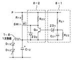
イグナイタ6は、HIDランプ5に2次巻線が直列に接続されて、その2次巻線において1次巻線側に発生するパルスを昇圧して出力するトランスT1と、トランスT1の1次巻線と閉回路を構成するコンデンサC12及びサイリスタD12と、ダイオードD13と、コンデンサC12を充電するためコンデンサC12に電源を供給する抵抗R13と、サイリスタD12のゲートに与えるゲート電圧を与えてそのオンタイミングを制御するための、抵抗R11,R12,コンデンサC11及びダイアックD11からなる制御手段と、抵抗R13に電圧が印加されている時間を計測するタイマー手段(8-1,8-2)と、抵抗R13に直列接続され、前記タイマー手段が所定時間以上前記抵抗R13に電圧が印加されていることを検出したときに、前記電源からコンデンサC12ヘの充電電流を遮断する遮断手段としてのスイッチ素子SW11と、備えている。
The
タイマー手段は、抵抗R13両端の電圧を検出する電圧検出部8-1と、その検出電圧に基づいてスイッチ素子SW11を制御してSW11のオン状態を遮断(オフ)する制御部8-2とを備えている。 The timer means includes a voltage detection unit 8-1 that detects the voltage across the resistor R13, and a control unit 8-2 that controls the switch element SW11 based on the detected voltage to shut off (turn off) the SW11. I have.
次に、上記構成の放電灯点灯装置の動作を図2乃至図6を参照して説明する。
図1の放電灯点灯装置に交流電源が投入されると、整流回路2の全波整流出力端の両端に接続した図示しない抵抗分圧回路により整流電圧を分圧した電圧が制御回路7に供給され且つ整流回路2の整流電圧が昇圧チョッパ回路3に供給されることで、昇圧チョッパ回路3のFETQ1の高周波(数十kHz)のオン,オフのスイッチング動作が開始される一方、イグナイタ6によってランプ始動パルスが発生されると同時にインバータ回路4のFETQ2,Q3における高周波(数十kHz)のオン,オフのスイッチング動作が開始される。インバータ回路4では、昇圧チョッパ回路3から安定化した直流電圧を入力し、先ずイグナイタ6の高圧パルスにてHIDランプ5を絶縁破壊して始動し、後述の図2(c)に示すような低周波の交流電流を生成してHIDランプ5を点灯しこれを維持する。
Next, the operation of the discharge lamp lighting device configured as described above will be described with reference to FIGS.
When the AC power supply is turned on in the discharge lamp lighting device of FIG. 1, a voltage obtained by dividing the rectified voltage by a resistance voltage dividing circuit (not shown) connected to both ends of the full-wave rectified output terminal of the
昇圧チョッパ回路3では、FETQ1がオンしている時にコイルL1にエネルギーを蓄え、FETQ1がオフの時にダイオードD5が導通し、コイルL1に蓄えられたエネルギーを、出力コンデンサである第1,第2の平滑コンデンサC2,C3の直列回路に向けて放出する。この時コイルL1に発生する電圧は入力電圧に直列に加算するので、出力電圧は入力電圧より高い電圧となる。高力率チョッパ回路として使用する場合は、毎サイクルコイルL1に蓄えたエネルギーが完全に放出する(即ち、コイルL1に流れる電流が0になる)電流モードで使用することが好ましい。 In the step-up chopper circuit 3, energy is stored in the coil L1 when the FET Q1 is on, the diode D5 is conducted when the FET Q1 is off, and the energy stored in the coil L1 is converted into the first and second output capacitors. It discharges toward the series circuit of smoothing capacitors C2 and C3. At this time, since the voltage generated in the coil L1 is added in series to the input voltage, the output voltage is higher than the input voltage. When used as a high power factor chopper circuit, it is preferable to use in a current mode in which the energy stored in the coil L1 is completely discharged (that is, the current flowing through the coil L1 becomes zero).
制御回路7はスイッチング素子であるFETQ1のゲートに対してスイッチングパルスを供給するが、昇圧チョッパ回路3の出力電圧である平滑コンデンサC2,C3の出力電圧に応じてそのスイッチングパルスのオン期間が制御され、結果としてFETQ1のオン時間をPWM制御し、出力コンデンサC2,C3らの出力電圧を安定化するよう制御する。
The
また、入力力率改善のために、FETQ1のオン時間の制御は、制御回路7が整流回路2の+全波整流電圧の振幅レベルを検出し、その振幅レベルに応じてFETQ1のオン時間を変えることによっても行われる。整流電圧の振幅レベルが小さいときほどFETQ1のオン時間を短く、整流電圧の振幅レベルが大きいときほどFETQ1のオン時間を長くなるように制御することにより、入力交流電流の波形は低周波(例えば50Hz)の正弦波状に整形され、入力交流電圧の波形と同期して変化するようになり、入力力率が改善される。
In order to improve the input power factor, the on-time of the FET Q1 is controlled by the
上記のように昇圧チョッパ回路3が動作を開始すると、イグナイタ6に電源が供給されると同時に、第1,第2のスイッチング素子であるFETQ2,Q3にスイッチングパルスが供給されることになる。これによって、イグナイタ6は高圧パルスを発生してHIDランプ5を放電状態(点灯状態)とし、FETQ2,Q3に高周波オン・オフのスイッチングパルスが与えられることになる。
When the step-up chopper circuit 3 starts operating as described above, power is supplied to the
図2(a)はFETQ2の高周波のオン・オフ動作を示し、図2(b)はFETQ3の高周波のオン・オフ動作を示している。図2(c)はHIDランプ5に流れる低周波のランプ電流を示している。
2A shows the high frequency on / off operation of the FET Q2, and FIG. 2B shows the high frequency on / off operation of the FET Q3. FIG. 2C shows a low-frequency lamp current flowing through the
このとき、制御回路7は、FETQ2,Q3がそれぞれの高周波スイッチング(例えば50kHz)のオンオフ動作を低周波(例えば100Hz)の一定周期Tで交互に繰返すように制御することによって、HIDランプ5には低周波の交流電力が供給されることになる。
At this time, the
インバータ回路4の動作を説明する。まず、周期Tの期間にFETQ2がオン・オフする動作について説明する。FETQ2のゲートにオンパルスが加えられて、FETQ2がオンしたときには、平滑コンデンサC2の充電電圧を電源として、C2→Q2→コイルL3→T1→HIDランプ5→R1→C2と電流が流れ、FETQ2がオフすると、コイルL3に蓄えられたエネルギーによって、コイルL3→T1→HIDランプ5→R1→C3→ダイオードD7→L3と電流が流れることにより、FETQ2が高周波スイッチング動作している期間Tでは常にHIDランプ5には、コイルL3→HIDランプ5→R1の方向に電流が流れることになる。
The operation of the
そして、次の周期Tの期間となると、FETQ3がオン・オフする動作に入る。FETQ3のゲートにオンパルスが加えられて、FETQ3がオンすると、平滑コンデンサC3の充電電圧を電源として、C3→R1→HIDランプ5→T1→コイルL3→Q3→C3と電流が流れ、FETQ3がオフすると、コイルL3に蓄えられたエネルギーによって、コイルL3→ダイオードD6→C2→R1→HIDランプ5→T1→L3と電流が流れることにより、FETQ3が高周波スイッチング動作している次の期間Tでは常にHIDランプ5には、R1→HIDランプ5→コイルL3の方向に電流が流れることになる。従って、HIDランプ5には、高周波駆動でありながら、図2(c)に示すような低周波のランプ電流が流れることになる。
In the next period T, the FET Q3 is turned on / off. When an ON pulse is applied to the gate of FET Q3 and FET Q3 is turned on, the current flows from C3 → R1 → HID
図2(c)に示す低周波のランプ電流には、FETQ2,Q3の高周波スイッチング動作により、高周波成分が重畳されるが、この高周波成分は第1のコンデンサとしてのコンデンサC4にてバイパスされるので、HIDランプ5を実際に流れるランプ電流には高周波成分はほとんど含まれず例えば100Hz(=周期2T)の低周波の矩形波(実線にて示す)にて点灯されることになる。
A high-frequency component is superimposed on the low-frequency lamp current shown in FIG. 2 (c) by the high-frequency switching operation of the FETs Q2 and Q3, but this high-frequency component is bypassed by the capacitor C4 as the first capacitor. The lamp current that actually flows through the
次に、イグナイタ6の動作について説明する。
交流電源投入時におけるパルス発生時には、平滑コンデンサC2,C3に充電される電圧に基づいてFETQ2,L3とダイオードD14を通してタイマー手段(8-1,8-2)に電圧が印加されると共に、抵抗R13とスイッチ素子SW11の直列回路を介して電流が流れ、第2のコンデンサとしてのコンデンサC12を充電する。
Next, the operation of the
When a pulse is generated when the AC power is turned on, a voltage is applied to the timer means (8-1, 8-2) through the FETs Q2, L3 and the diode D14 based on the voltage charged in the smoothing capacitors C2, C3, and the resistor R13. A current flows through the series circuit of the switch element SW11 and charges the capacitor C12 as the second capacitor.
このとき同時に、昇圧チョッパ回路3の平滑コンデンサ出力端の出力電圧が、抵抗R11と、抵抗R12及びコンデンサC11の並列回路とを直列接続した回路の両端に加えられ、その接続点の電圧(コンデンサC11の電圧)がダイアックD11のブレークオーバー電圧を越えると、サイリスタD12のゲートに電圧が加えられてサイリスタD12はオンする。 At the same time, the output voltage of the smoothing capacitor output terminal of the step-up chopper circuit 3 is applied to both ends of a circuit in which a resistor R11 and a parallel circuit of the resistor R12 and the capacitor C11 are connected in series, and the voltage at the connection point (capacitor C11). ) Exceeds the breakover voltage of the diac D11, a voltage is applied to the gate of the thyristor D12 and the thyristor D12 is turned on.
サイリスタD12のオンタイミング制御信号によりサイリスタD12がオンするとコンデンサC12の充電電荷がトランスT1の1次巻線を通して放電し、その際、C12とT1の1次巻線の共振に基づいてパルスが発生する。このパルスはトランスT1の巻線比に基づいて昇圧されて、放電ランプ5に直列接続したトランスT1の2次巻線に高圧パルスを発生する。
When the thyristor D12 is turned on by the ON timing control signal of the thyristor D12, the charge of the capacitor C12 is discharged through the primary winding of the transformer T1, and at this time, a pulse is generated based on the resonance of the primary windings of C12 and T1. . This pulse is boosted based on the winding ratio of the transformer T1, and a high voltage pulse is generated in the secondary winding of the transformer T1 connected in series with the
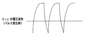
図3はパルス発生時のコンデンサC12の波形例を示し、図4はパルス発生時の抵抗R13の波形例を示している。通常は、C12とT1の1次巻線との共振に基づく振動波形によって、サイリスタD12に逆電圧が印加されるのでサイリスタD12はオフする。(すなわち、サイリスタD12がオンすると、コンデンサC12のエネルギーはほぼコンデンサC12のコンデンサ容量とイグナイタトランスT1の1次巻線のインダクタンスの共振周波数による振動波形となり,サイリスタD12に逆電圧が印加される。)
しかし、サイリスタD12には温度特性があり、高温になるとサイリスタD12のオフ特性が悪くなりオフしにくくなったり、ランプ始動時のランプ電流の影響により、1次側インダクタンスが低下し、サイリスタD12がオフできない場合がある。すなわち、ランプ始動時には、イグナイタ6のトランスT1の2次側に電流が流れるので、イグナイタ6のトランスT1の1次側インダクタンスは極端に低下する。すると、サイリスタD12オン時の振動周波数は始動前よりも高くなり、また振動もすぐに減衰するため、サイリスタD12がオフできにくくなる傾向にある。
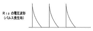
FIG. 3 shows a waveform example of the capacitor C12 at the time of pulse generation, and FIG. 4 shows a waveform example of the resistor R13 at the time of pulse generation. Normally, a reverse voltage is applied to the thyristor D12 by a vibration waveform based on resonance between C12 and the primary winding of T1, so that the thyristor D12 is turned off. (That is, when the thyristor D12 is turned on, the energy of the capacitor C12 substantially becomes a vibration waveform by the resonance frequency of the capacitor capacity of the capacitor C12 and the inductance of the primary winding of the igniter transformer T1, and a reverse voltage is applied to the thyristor D12.)
However, the thyristor D12 has a temperature characteristic. When the temperature becomes high, the off-characteristic of the thyristor D12 deteriorates and it is difficult to turn off, or the primary inductance decreases due to the influence of the lamp current at the start of the lamp, and the thyristor D12 is turned off. There are cases where it is not possible. That is, at the time of starting the lamp, since a current flows to the secondary side of the transformer T1 of the
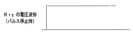
ここで、電圧検出部8-1と制御部8-2とを備えた本発明に係るタイマー手段が無い場合について説明すると、上記のようにサイリスタD12がオフできなくなると、電流がダイオードD14を通して抵抗R13とサイリスタD12に(保持電流以上に)流れ続け、パルス発生が停止してしまうとともに、抵抗R13での損失が発生する。図5は、タイマー手段が無くサイリスタD12を経て電流が流れ続けている時の抵抗R13の電圧波形を示している。 Here, the case where there is no timer means according to the present invention provided with the voltage detection unit 8-1 and the control unit 8-2 will be described. When the thyristor D12 cannot be turned off as described above, the current is passed through the diode D14. It continues to flow through R13 and thyristor D12 (more than the holding current), the pulse generation stops, and a loss at resistor R13 occurs. FIG. 5 shows the voltage waveform of the resistor R13 when there is no timer means and current continues to flow through the thyristor D12.
そこで、図1の本発明の実施例1においては、抵抗R13の電圧を検出し、電圧が連続的に印加されている時間をタイマー手段により計測し、所定時間以上前記抵抗R13に電圧が印加されていることを検出したときに、サイリスタD12がオフできずオンし続けていると判断し、スイッチ素子SW11をオフにして、抵抗R13に流れる電流を遮断する。一度遮断するとサイリスタD12には電流が流れなくなるので(保持電流以下になるため)サイリスタD12は確実にオフする。 Therefore, in the first embodiment of the present invention shown in FIG. 1, the voltage of the resistor R13 is detected, the time during which the voltage is continuously applied is measured by timer means, and the voltage is applied to the resistor R13 for a predetermined time or more. When it is detected that the thyristor D12 cannot be turned off, it is determined that the thyristor D12 cannot be turned off and continues to be turned on. The switch element SW11 is turned off to interrupt the current flowing through the resistor R13. Once interrupted, no current flows through the thyristor D12 (because it is below the holding current), so that the thyristor D12 is reliably turned off.
図6は図1の上記タイマー手段(8-1,8-2)の一実施例を示す回路図である。
図6では、平滑コンデンサC2,C3に充電される電圧に基づいてQ2,L3とダイオードD14を通して電圧が供給される電源ラインPと前記充電用のコンデンサC12の+電圧出力端との間に、前記抵抗R13と遮断用のスイッチ素子SW11との直列回路を接続してある。スイッチ素子SW11としてはNチャネルトランジスタを用いている。そして、抵抗R13とスイッチ素子SW11の直列回路に並列に、抵抗R13に電圧が発生していることを検出するための電圧検出部8-1を接続すると共に、その検出電圧に基づいてスイッチ素子SW11を遮断(オフ)するための制御部8-2を接続してある。
FIG. 6 is a circuit diagram showing an embodiment of the timer means (8-1, 8-2) shown in FIG.
In FIG. 6, based on the voltage charged to the smoothing capacitors C2 and C3, between the power supply line P to which the voltage is supplied through Q2 and L3 and the diode D14, and the positive voltage output terminal of the charging capacitor C12, A series circuit of a resistor R13 and a blocking switch element SW11 is connected. An N channel transistor is used as the switch element SW11. A voltage detector 8-1 for detecting that a voltage is generated in the resistor R13 is connected in parallel with the series circuit of the resistor R13 and the switch element SW11. Based on the detected voltage, the switch element SW11 is connected. A control unit 8-2 for shutting off (turning off) is connected.
電圧検出部8-1は、一端部が電源ラインPと前記スイッチ素子SW11のソース(即ちコンデンサC12の+電圧出力端)の間に、抵抗R21と、抵抗R22及びコンデンサC21の並列回路とを直列に接続した直列回路を接続し、R21とC21(R22)の接続点にツェナーダイオードZD1のカソードを接続して構成されている。 The voltage detector 8-1 has one end connected in series with a resistor R21 and a parallel circuit of the resistor R22 and the capacitor C21 between the power line P and the source of the switch element SW11 (that is, the + voltage output end of the capacitor C12). And a cathode of a Zener diode ZD1 is connected to a connection point between R21 and C21 (R22).
また、制御部8-2は、一端部が電源ラインPと前記スイッチ素子SW11のソース(即ちコンデンサC12の+電圧出力端)との間に、抵抗R23と、バイポーラトランジスタQ4のコレクタ・エミッタとを直列に接続した直列回路を接続し、トランジスタQ4のコレクタを前記スイッチ素子SW11のゲートに接続し、トランジスタQ4のコレクタ・エミッタ間(即ちスイッチ素子SW11のゲート・ソース間)にツェナーダイオードZD2を接続して構成されている。 The control unit 8-2 has a resistor R23 and a collector / emitter of the bipolar transistor Q4 between one end of the power supply line P and the source of the switch element SW11 (that is, the + voltage output terminal of the capacitor C12). A series circuit connected in series is connected, the collector of the transistor Q4 is connected to the gate of the switch element SW11, and a Zener diode ZD2 is connected between the collector and emitter of the transistor Q4 (that is, between the gate and source of the switch element SW11). Configured.
次に、図6の動作を説明する。ここで、トランスT1のパルス発生によってHIDランプ5が始動するが、サイリスタD12がオフせずにオンしたままであるとする。
Next, the operation of FIG. 6 will be described. Here, it is assumed that the
図6に示すタイマー手段(8-1,8-2)では、電源ラインPの電圧が抵抗R23を介してスイッチ素子SW11のゲートに印加されるので、最初は抵抗R23によりスイッチ素子SW11がオンしている。抵抗R13に電圧が印加されている間は、抵抗R23によりツェナーダイオードZD2にはツェナー電圧が発生して、スイッチ素子SW11のゲート・ソース間電圧はZD2のツェナー電圧に保持される。抵抗R13に電圧が印加されている間、電圧検出部8-1では、抵抗R21によりコンデンサC21が充電される。この充電時間が一定時間以上になるとC21の充電電圧がツェナーダイオードZD1のツェナーレベルを越えるので、ZD1がオンしてバイポーラトランジスタQ4のベースに順バイアスが与えられてQ4がオンする。これにより、スイッチ素子SW11のゲート・ソース間が同電位になることで、スイッチ素子SW11は遮断(オフ)する。 In the timer means (8-1, 8-2) shown in FIG. 6, since the voltage of the power supply line P is applied to the gate of the switch element SW11 via the resistor R23, the switch element SW11 is initially turned on by the resistor R23. ing. While the voltage is applied to the resistor R13, a Zener voltage is generated in the Zener diode ZD2 by the resistor R23, and the gate-source voltage of the switch element SW11 is held at the Zener voltage of ZD2. While the voltage is applied to the resistor R13, in the voltage detector 8-1, the capacitor C21 is charged by the resistor R21. When the charging time exceeds a certain time, the charging voltage of C21 exceeds the Zener level of the Zener diode ZD1, so that ZD1 is turned on, a forward bias is applied to the base of the bipolar transistor Q4, and Q4 is turned on. As a result, the switch element SW11 is cut off (turned off) when the gate and source of the switch element SW11 have the same potential.
本発明の実施例1によれば、サイリスタD12がオフできずにオンし続けた場合には、、抵抗に連続した一定の電流が流れるので、抵抗R13に発生する電圧を検知し、この電圧検出に基づいて抵抗R13からサイリスタD12ヘ流れる電流を遮断してサイリスタD12をオフし、再び高圧パルスの発生を可能とする。 According to the first embodiment of the present invention, when the thyristor D12 cannot be turned off and continues to be turned on, a constant current flowing through the resistor flows. Therefore, the voltage generated in the resistor R13 is detected, and this voltage detection is performed. Based on the above, the current flowing from the resistor R13 to the thyristor D12 is cut off to turn off the thyristor D12, and the high voltage pulse can be generated again.
図7本発明の実施例2の放電灯点灯装置の回路図である。本実施例2の放電灯点灯装置10Aは、実施例1の放電灯点灯装置10とは、インバータ回路内におけるイグナイタの構成が異なっている。その他の、交流電源1、整流回路2、昇圧チョッパ回路3は、実施例1と同様である。また、イグナイタ6Aを除いたインバータ回路部分の構成も、実施例1と同様である。
7 is a circuit diagram of a discharge lamp lighting device of Example 2 of the present invention. The discharge
イグナイタ6Aは、HIDランプ5に2次巻線が直列に接続されて、その2次巻線において1次巻線側に発生するパルスを昇圧して出力するトランスT1と、トランスT1の1次巻線と閉回路を構成するコンデンサC12及びサイリスタD12と、コンデンサC12を充電するためコンデンサC12に電源を供給する抵抗R13と、サイリスタD12のゲートに与えるゲート電圧を与えてオンタイミングを制御するための、抵抗R11,R12,コンデンサC11及びダイアックD11からなる制御手段と、抵抗R13の温度を検出する温度検出部9と、抵抗R13に直列接続され、前記温度検出部9が前記抵抗R13の温度が一定値以上あることを検出したときに、前記電源からコンデンサC12ヘの充電電流を遮断する遮断手段としてのスイッチ素子SW12と、備えている。
The igniter 6A includes a transformer T1 having a secondary winding connected in series to the
図8は図7の上記温度検出部9及びスイッチ素子SW12による温度反応型スイッチ素子の一実施例を模式的に示す構成図である。
FIG. 8 is a block diagram schematically showing an embodiment of a temperature-responsive switch element including the
図8に示す温度反応型スイッチ素子は、同一のベース部材上に、被検体である抵抗R13の本体部に接着させて抵抗R13の温度を直接感知する温度検出部9と、該温度検出部9に近接して設けられて、温度に反応して自動的に接点が切れるバイメタル式の機械的なスイッチ素子SW12とを組み合せたスイッチである。このような熱応動スイッチは、過熱保護手段の一つであって、抵抗の温度が一定の温度を越えると、自動的に接点を切って、電流を遮断するサーマルプロテクタと呼ばれているものである。
The temperature-responsive switch element shown in FIG. 8 is bonded to the body of a resistor R13, which is a subject, on the same base member, and directly detects the temperature of the resistor R13, and the
なお、温度検出部9としてはサーミスタ(温度上昇により抵抗値が減少或いは上昇する素子)のような温度センサを用いた温度検出回路で構成することもでき、その検出信号にてFETなどの半導体スイッチで構成されるスイッチ素子SW12をオフにする構成としてもよい。
The
次に、図7のイグナイタ6Aの動作を説明する。
交流電源投入時におけるパルス発生時には、平滑コンデンサC2,C3に充電される電圧に基づいてQ2,L3とダイオードD14を通して電圧が加えられると、スイッチ素子SW12及び抵抗R13の直列回路を介して電流が流れ、第2のコンデンサとしてのコンデンサC12を充電する。この抵抗R13と直列に図8に示すような温度反応型スイッチ素子からなるサーマルプロテクタを接続している。
HIDランプ5が始動する前には、サイリスタD12がオンすると、コンデンサC12に充電されたエネルギーはほぼコンデンサC12のコンデンサ容量とイグナイタ6AのトランスT1の1次巻線のインダクタンスの共振周波数による振動波形で、サイリスタD12に逆電圧が印加される。
Next, the operation of the igniter 6A in FIG. 7 will be described.
When a pulse is generated when the AC power is turned on, if a voltage is applied through Q2 and L3 and the diode D14 based on the voltage charged in the smoothing capacitors C2 and C3, a current flows through the series circuit of the switch element SW12 and the resistor R13. The capacitor C12 as the second capacitor is charged. A thermal protector composed of a temperature-responsive switch element as shown in FIG. 8 is connected in series with the resistor R13.
When the thyristor D12 is turned on before the
一方、HIDランプ5が始動する際には、イグナイタ6AのトランスT1の2次側に電流が流れるので、イグナイタ6AのトランスT1の1次側インダクタンスは極端に低下する。従って、共振周波数は始動前よりも高く、また振動もすぐに減衰するため、サイリスタD12がオフできる十分な時間をもつ逆電圧を印加できなくなる傾向にある。
On the other hand, when the
ここで、トランスT1の1次巻線におけるパルス発生によってHIDランプ5が始動するが、上記のような理由によって、サイリスタD12がオフすることができずにオンしたままであるとする。サイリスタD12がオンし続けるとコンデンサC12には電流が流れず、抵抗R13からトランスT1の1次巻線を経由してサイリスタD12に電流が流れ続ける。この時に抵抗R13での消費電力が通常より大きくなり温度が上昇する。これをサーマルプロテクタが検出すると、抵抗R13に流れる電流を遮断する。一度遮断するとサイリスタD12には電流が流れなくなるので(保持電流以下になるため)サイリスタD12はオフする。
Here, it is assumed that the
本発明の実施例2によれば、サイリスタD12がオフできずにオンし続けた場合には、抵抗に連続した一定の電流が流れるので、抵抗R13に発生する温度を検知し、この温度検出に基づいて抵抗R13からサイリスタD12ヘ流れる電流を遮断してサイリスタD12をオフし、再び高圧パルスの発生を可能とする。 According to the second embodiment of the present invention, when the thyristor D12 cannot be turned off and continues to be turned on, a constant current flowing through the resistor flows. Therefore, the temperature generated in the resistor R13 is detected, and this temperature detection is performed. Based on this, the current flowing from the resistor R13 to the thyristor D12 is cut off, the thyristor D12 is turned off, and a high voltage pulse can be generated again.
図9は、図1又は図7の上記放電灯点灯装置を用いた、本発明の照明装置の実施例を示す断面図である。
図9において、符号11は照明器具本体であり、12は反射傘である。照明器具本体11の反射傘12の適宜の位置(例えば中心)に放電ランプであるHIDランプ5が装着されて保持される。また、照明器具本体11内には図1又は図7で説明した構成からなる放電灯点灯装置10又は10Aが配設されている。
FIG. 9 is a cross-sectional view showing an embodiment of the illumination device of the present invention using the discharge lamp lighting device of FIG. 1 or FIG.
In FIG. 9, the code |
このように図1又は図7の放電灯点灯装置10又は10Aを用いた照明装置によれば、ランプ始動後にサイリスタを確実にオフでき、電源を供給するための抵抗が加熱して劣化を招くのを防ぐと共に、無駄な電力消費が発生するのを防止できる。
As described above, according to the lighting device using the discharge
本発明は、水銀ランプ、メタルハライドランプ、高圧ナトリウムランプなどのHIDランプのほか、キセノンランプを含む高圧放電点灯装置のイグナイタにおいて、充電用コンデンサへの電源供給用の抵抗の過熱防止に応用することが可能である。 INDUSTRIAL APPLICABILITY The present invention can be applied to prevent overheating of a resistor for supplying power to a charging capacitor in an igniter of a high pressure discharge lighting device including a HID lamp such as a mercury lamp, a metal halide lamp, a high pressure sodium lamp, and a xenon lamp. Is possible.
1…交流電源
2…整流回路
3…昇圧チョッパ回路(直流電源)
4…インバータ回路
5…HIDランプ(放電ランプ)
10,10A…放電灯点灯装置
R1〜R3…抵抗(イグナイタへの始動時の電源供給用)
C2,C3…第1,第2の平滑コンデンサ
Q2,Q3…FET(第1,第2のスイッチング素子)
L3…コイル(インダクタ)
C4…コンデンサ(第1のコンデンサ)
D12…サイリスタ
C12…コンデンサ(第2のコンデンサ)
SW11,SW12…スイッチ素子(遮断手段)
R13…抵抗(コンデンサへの電源供給用)
8-1…電圧検出部
8-2…制御部
9…温度検出部
代理人 弁理士 伊 藤 進
DESCRIPTION OF
4 ...
10, 10A ... discharge lamp lighting device R1 ~ R3 ... resistance (for power supply when starting to igniter)
C2, C3 ... first and second smoothing capacitors Q2, Q3 ... FET (first and second switching elements)
L3 ... Coil (inductor)
C4 ... Capacitor (first capacitor)
D12 ... Thyristor C12 ... Capacitor (second capacitor)
SW11, SW12 ... switch element (blocking means)
R13 ... resistor (for power supply to capacitor)
8-1 Voltage detection unit 8-2
Agent Patent Attorney Susumu Ito
Claims (5)
放電ランプと前記トランスの2次巻線の直列回路と並列に接続される第1のコンデンサと;
前記トランスの1次巻線と閉回路を構成する第2のコンデンサとサイリスタと;
前記第2のコンデンサに電源を供給する抵抗と;
前記サイリスタのオンタイミングを制御する制御手段と;
前記抵抗に電圧が印加されている時間を計測するタイマー手段と;
前記抵抗に直列接続され、前記タイマー手段が所定時間以上前記抵抗に電圧が印加されていることを検出したときに、前記電源から前記第2のコンデンサヘの充電電流を遮断する遮断手段と;
を具備したことを特徴とするパルス発生回路。 A transformer in which a secondary winding is connected in series to a discharge lamp, and a pulse generated in the primary winding is boosted and output to the secondary winding;
A first capacitor connected in parallel with a series circuit of a discharge lamp and a secondary winding of the transformer;
A second capacitor and a thyristor constituting a closed circuit with the primary winding of the transformer;
A resistor for supplying power to the second capacitor;
Control means for controlling the on-timing of the thyristor;
Timer means for measuring the time during which voltage is applied to the resistor;
A shut-off means connected in series to the resistor, and shuts off a charging current from the power source to the second capacitor when the timer means detects that a voltage is applied to the resistor for a predetermined time or more;
A pulse generation circuit comprising:
放電ランプと前記トランスの2次巻線の直列回路と並列に接続される第1のコンデンサと;
前記トランスの1次巻線と閉回路を構成する第2のコンデンサとサイリスタと;
前記第2のコンデンサに電源を供給する抵抗と;
前記サイリスタのオンタイミングを制御する制御手段と;
前記抵抗の温度を検出する温度検出部を備え、且つ前記抵抗に直列接続され、前記抵抗の温度が所定値以上であることを検出したときに、前記電源から前記第2のコンデンサヘの充電電流を遮断する温度反応型スイッチ素子と;
を具備したことを特徴とするパルス発生回路。 A transformer in which a secondary winding is connected in series to a discharge lamp, and a pulse generated in the primary winding is boosted and output to the secondary winding;
A first capacitor connected in parallel with a series circuit of a discharge lamp and a secondary winding of the transformer;
A second capacitor and a thyristor constituting a closed circuit with the primary winding of the transformer;
A resistor for supplying power to the second capacitor;
Control means for controlling the on-timing of the thyristor;
A temperature detection unit that detects the temperature of the resistor, and is connected in series to the resistor, and when it is detected that the temperature of the resistor is equal to or higher than a predetermined value, a charging current from the power source to the second capacitor A temperature-responsive switch element that shuts off
A pulse generation circuit comprising:
前記直流電圧源に接続されて、交流電力を生成して放電ランプの点灯を維持させるインバータ回路と;
前記インバータ回路に組み込まれて、昇圧パルスにて前記放電ランプを始動させる請求項1乃至3のいずか1つに記載のパルス発生回路と;
を具備したことを特徴とする放電灯点灯装置。 A DC voltage source for generating a DC voltage from the output of the AC power supply;
An inverter circuit connected to the DC voltage source for generating AC power and maintaining the discharge lamp on;
4. The pulse generation circuit according to claim 1, wherein the pulse generation circuit is incorporated in the inverter circuit and starts the discharge lamp with a boost pulse. 5.
A discharge lamp lighting device comprising:
放電ランプとしてのHIDランプと;
前記HIDランプを保持する器具本体と;
を具備したことを特徴とする照明装置。
A discharge lamp lighting device according to claim 4;
An HID lamp as a discharge lamp;
An instrument body holding the HID lamp;
An illumination device comprising:
Priority Applications (1)
| Application Number | Priority Date | Filing Date | Title |
|---|---|---|---|
| JP2004336430A JP2006147367A (en) | 2004-11-19 | 2004-11-19 | Pulse generation circuit, discharge lamp lighting device and lighting system |
Applications Claiming Priority (1)
| Application Number | Priority Date | Filing Date | Title |
|---|---|---|---|
| JP2004336430A JP2006147367A (en) | 2004-11-19 | 2004-11-19 | Pulse generation circuit, discharge lamp lighting device and lighting system |
Publications (1)
| Publication Number | Publication Date |
|---|---|
| JP2006147367A true JP2006147367A (en) | 2006-06-08 |
Family
ID=36626802
Family Applications (1)
| Application Number | Title | Priority Date | Filing Date |
|---|---|---|---|
| JP2004336430A Withdrawn JP2006147367A (en) | 2004-11-19 | 2004-11-19 | Pulse generation circuit, discharge lamp lighting device and lighting system |
Country Status (1)
| Country | Link |
|---|---|
| JP (1) | JP2006147367A (en) |
Cited By (3)
| Publication number | Priority date | Publication date | Assignee | Title |
|---|---|---|---|---|
| JP2011018559A (en) * | 2009-07-09 | 2011-01-27 | Mitsubishi Electric Corp | Discharge lamp lighting device and lighting fixture equipped with the same |
| JP5170095B2 (en) * | 2007-07-09 | 2013-03-27 | 株式会社村田製作所 | High pressure discharge lamp lighting device |
| CN109507487A (en) * | 2018-11-21 | 2019-03-22 | 华自科技股份有限公司 | Thyristor triggering impulse signal deteching circuit |
-
2004
- 2004-11-19 JP JP2004336430A patent/JP2006147367A/en not_active Withdrawn
Cited By (3)
| Publication number | Priority date | Publication date | Assignee | Title |
|---|---|---|---|---|
| JP5170095B2 (en) * | 2007-07-09 | 2013-03-27 | 株式会社村田製作所 | High pressure discharge lamp lighting device |
| JP2011018559A (en) * | 2009-07-09 | 2011-01-27 | Mitsubishi Electric Corp | Discharge lamp lighting device and lighting fixture equipped with the same |
| CN109507487A (en) * | 2018-11-21 | 2019-03-22 | 华自科技股份有限公司 | Thyristor triggering impulse signal deteching circuit |
Similar Documents
| Publication | Publication Date | Title |
|---|---|---|
| JP5302755B2 (en) | Power supply | |
| CA2657783A1 (en) | High-pressure discharge lamp lighting device and lighting fixture using the same | |
| JP2010044979A (en) | High-pressure discharge lamp lighting device, and illumination apparatus | |
| CA2848600A1 (en) | Starting circuit for buck converter | |
| KR20080100138A (en) | Program start ballast | |
| TW200904252A (en) | Power supply for halogen lamp | |
| JP3042470B2 (en) | Lighting device for discharge lamp and lighting device for discharge lamp | |
| JP2006147367A (en) | Pulse generation circuit, discharge lamp lighting device and lighting system | |
| US6936970B2 (en) | Method and apparatus for a unidirectional switching, current limited cutoff circuit for an electronic ballast | |
| JP3971808B2 (en) | Discharge lamp lighting device | |
| JP4752136B2 (en) | Discharge lamp lighting device | |
| JP2010080138A (en) | High-pressure discharge lamp lighting device, and lighting fixture | |
| JP5460065B2 (en) | Discharge lamp lighting circuit | |
| JP2005251722A (en) | High pressure discharge lamp lighting device, starting device and illuminating device | |
| KR200215723Y1 (en) | An electronic ballast for lighting metal halide discharge lamp | |
| JP3820865B2 (en) | Power supply | |
| JP4088049B2 (en) | Discharge lamp lighting device | |
| KR200215724Y1 (en) | An electronic ballast for lighting metal halide discharge lamp | |
| JP3763837B2 (en) | Fluorescent lamp lighting device | |
| JP2006302599A (en) | Discharge lamp lighting device | |
| JP2006156345A (en) | Discharge lamp lighting device and luminaire | |
| JP2002352972A (en) | Lighting equipment for electric discharge lamp | |
| JPH10289789A (en) | Discharge lamp lighting device | |
| JP2005174610A (en) | Lighting system | |
| JPH0244698A (en) | Discharge lamp lighting device |
Legal Events
| Date | Code | Title | Description |
|---|---|---|---|
| A621 | Written request for application examination |
Free format text: JAPANESE INTERMEDIATE CODE: A621 Effective date: 20071031 |
|
| A761 | Written withdrawal of application |
Free format text: JAPANESE INTERMEDIATE CODE: A761 Effective date: 20091202 |