JP2006120870A - Wire formation method and device thereof - Google Patents
Wire formation method and device thereof Download PDFInfo
- Publication number
- JP2006120870A JP2006120870A JP2004307354A JP2004307354A JP2006120870A JP 2006120870 A JP2006120870 A JP 2006120870A JP 2004307354 A JP2004307354 A JP 2004307354A JP 2004307354 A JP2004307354 A JP 2004307354A JP 2006120870 A JP2006120870 A JP 2006120870A
- Authority
- JP
- Japan
- Prior art keywords
- wiring
- film
- conductive film
- forming
- substrate
- Prior art date
- Legal status (The legal status is an assumption and is not a legal conclusion. Google has not performed a legal analysis and makes no representation as to the accuracy of the status listed.)
- Pending
Links
Images


Classifications
-
- H—ELECTRICITY
- H01—ELECTRIC ELEMENTS
- H01L—SEMICONDUCTOR DEVICES NOT COVERED BY CLASS H10
- H01L21/00—Processes or apparatus adapted for the manufacture or treatment of semiconductor or solid state devices or of parts thereof
- H01L21/70—Manufacture or treatment of devices consisting of a plurality of solid state components formed in or on a common substrate or of parts thereof; Manufacture of integrated circuit devices or of parts thereof
- H01L21/71—Manufacture of specific parts of devices defined in group H01L21/70
- H01L21/768—Applying interconnections to be used for carrying current between separate components within a device comprising conductors and dielectrics
- H01L21/76838—Applying interconnections to be used for carrying current between separate components within a device comprising conductors and dielectrics characterised by the formation and the after-treatment of the conductors
- H01L21/76841—Barrier, adhesion or liner layers
- H01L21/76871—Layers specifically deposited to enhance or enable the nucleation of further layers, i.e. seed layers
- H01L21/76873—Layers specifically deposited to enhance or enable the nucleation of further layers, i.e. seed layers for electroplating
-
- C—CHEMISTRY; METALLURGY
- C25—ELECTROLYTIC OR ELECTROPHORETIC PROCESSES; APPARATUS THEREFOR
- C25D—PROCESSES FOR THE ELECTROLYTIC OR ELECTROPHORETIC PRODUCTION OF COATINGS; ELECTROFORMING; APPARATUS THEREFOR
- C25D17/00—Constructional parts, or assemblies thereof, of cells for electrolytic coating
- C25D17/001—Apparatus specially adapted for electrolytic coating of wafers, e.g. semiconductors or solar cells
-
- C—CHEMISTRY; METALLURGY
- C25—ELECTROLYTIC OR ELECTROPHORETIC PROCESSES; APPARATUS THEREFOR
- C25D—PROCESSES FOR THE ELECTROLYTIC OR ELECTROPHORETIC PRODUCTION OF COATINGS; ELECTROFORMING; APPARATUS THEREFOR
- C25D7/00—Electroplating characterised by the article coated
- C25D7/12—Semiconductors
- C25D7/123—Semiconductors first coated with a seed layer or a conductive layer
-
- H—ELECTRICITY
- H01—ELECTRIC ELEMENTS
- H01L—SEMICONDUCTOR DEVICES NOT COVERED BY CLASS H10
- H01L21/00—Processes or apparatus adapted for the manufacture or treatment of semiconductor or solid state devices or of parts thereof
- H01L21/02—Manufacture or treatment of semiconductor devices or of parts thereof
- H01L21/04—Manufacture or treatment of semiconductor devices or of parts thereof the devices having at least one potential-jump barrier or surface barrier, e.g. PN junction, depletion layer or carrier concentration layer
- H01L21/18—Manufacture or treatment of semiconductor devices or of parts thereof the devices having at least one potential-jump barrier or surface barrier, e.g. PN junction, depletion layer or carrier concentration layer the devices having semiconductor bodies comprising elements of Group IV of the Periodic System or AIIIBV compounds with or without impurities, e.g. doping materials
- H01L21/28—Manufacture of electrodes on semiconductor bodies using processes or apparatus not provided for in groups H01L21/20 - H01L21/268
- H01L21/283—Deposition of conductive or insulating materials for electrodes conducting electric current
- H01L21/288—Deposition of conductive or insulating materials for electrodes conducting electric current from a liquid, e.g. electrolytic deposition
-
- H—ELECTRICITY
- H01—ELECTRIC ELEMENTS
- H01L—SEMICONDUCTOR DEVICES NOT COVERED BY CLASS H10
- H01L21/00—Processes or apparatus adapted for the manufacture or treatment of semiconductor or solid state devices or of parts thereof
- H01L21/02—Manufacture or treatment of semiconductor devices or of parts thereof
- H01L21/04—Manufacture or treatment of semiconductor devices or of parts thereof the devices having at least one potential-jump barrier or surface barrier, e.g. PN junction, depletion layer or carrier concentration layer
- H01L21/18—Manufacture or treatment of semiconductor devices or of parts thereof the devices having at least one potential-jump barrier or surface barrier, e.g. PN junction, depletion layer or carrier concentration layer the devices having semiconductor bodies comprising elements of Group IV of the Periodic System or AIIIBV compounds with or without impurities, e.g. doping materials
- H01L21/30—Treatment of semiconductor bodies using processes or apparatus not provided for in groups H01L21/20 - H01L21/26
- H01L21/31—Treatment of semiconductor bodies using processes or apparatus not provided for in groups H01L21/20 - H01L21/26 to form insulating layers thereon, e.g. for masking or by using photolithographic techniques; After treatment of these layers; Selection of materials for these layers
- H01L21/3205—Deposition of non-insulating-, e.g. conductive- or resistive-, layers on insulating layers; After-treatment of these layers
- H01L21/321—After treatment
- H01L21/32115—Planarisation
- H01L21/3212—Planarisation by chemical mechanical polishing [CMP]
- H01L21/32125—Planarisation by chemical mechanical polishing [CMP] by simultaneously passing an electrical current, i.e. electrochemical mechanical polishing, e.g. ECMP
-
- H—ELECTRICITY
- H01—ELECTRIC ELEMENTS
- H01L—SEMICONDUCTOR DEVICES NOT COVERED BY CLASS H10
- H01L21/00—Processes or apparatus adapted for the manufacture or treatment of semiconductor or solid state devices or of parts thereof
- H01L21/70—Manufacture or treatment of devices consisting of a plurality of solid state components formed in or on a common substrate or of parts thereof; Manufacture of integrated circuit devices or of parts thereof
- H01L21/71—Manufacture of specific parts of devices defined in group H01L21/70
- H01L21/768—Applying interconnections to be used for carrying current between separate components within a device comprising conductors and dielectrics
- H01L21/76838—Applying interconnections to be used for carrying current between separate components within a device comprising conductors and dielectrics characterised by the formation and the after-treatment of the conductors
- H01L21/76841—Barrier, adhesion or liner layers
- H01L21/76843—Barrier, adhesion or liner layers formed in openings in a dielectric
- H01L21/76849—Barrier, adhesion or liner layers formed in openings in a dielectric the layer being positioned on top of the main fill metal
-
- H—ELECTRICITY
- H01—ELECTRIC ELEMENTS
- H01L—SEMICONDUCTOR DEVICES NOT COVERED BY CLASS H10
- H01L21/00—Processes or apparatus adapted for the manufacture or treatment of semiconductor or solid state devices or of parts thereof
- H01L21/70—Manufacture or treatment of devices consisting of a plurality of solid state components formed in or on a common substrate or of parts thereof; Manufacture of integrated circuit devices or of parts thereof
- H01L21/71—Manufacture of specific parts of devices defined in group H01L21/70
- H01L21/768—Applying interconnections to be used for carrying current between separate components within a device comprising conductors and dielectrics
- H01L21/76838—Applying interconnections to be used for carrying current between separate components within a device comprising conductors and dielectrics characterised by the formation and the after-treatment of the conductors
- H01L21/76877—Filling of holes, grooves or trenches, e.g. vias, with conductive material
Abstract
Description
本発明は、配線形成方法及び装置に係り、特に半導体ウエハ等の基板の表面に設けた配線用凹部に銅や銀等の導電体(配線材料)を埋込んで埋込み配線を形成したり、更にはこの埋込み配線の表面を金属膜(保護膜)で選択的に覆って多層構造としたりするのに使用される配線形成方法及び装置に関する。 The present invention relates to a wiring formation method and apparatus, and more particularly to form a buried wiring by embedding a conductor (wiring material) such as copper or silver in a wiring recess provided on the surface of a substrate such as a semiconductor wafer. Relates to a wiring forming method and apparatus used for selectively covering the surface of the embedded wiring with a metal film (protective film) to form a multilayer structure.
半導体装置の配線形成プロセスとして、トレンチ及びビアホールからなる配線用凹部に配線材料(金属)を埋込むようにしたプロセス(いわゆる、ダマシンプロセス)が使用されつつある。これは、層間絶縁膜に予め形成したトレンチやビアホール等の配線用凹部に、アルミニウム、近年では銅や銀等の配線材料(金属)を埋め込んだ後、余分な金属を化学機械的研磨(CMP)によって除去し平坦化するプロセス技術である。 As a wiring formation process of a semiconductor device, a process (so-called damascene process) in which a wiring material (metal) is buried in a wiring recess made of a trench and a via hole is being used. This is because, after embedding a wiring material (metal) such as aluminum or copper or silver in a recess for wiring such as a trench or a via hole previously formed in an interlayer insulating film, the excess metal is subjected to chemical mechanical polishing (CMP). This is a process technology for removing and flattening by means of.
この種の配線、例えば配線材料として銅を使用した銅配線にあっては、層間絶縁膜への銅の拡散を防止するため、層間絶縁膜の表面にタングステン、タンタルまたはチタンのいずれかを含むバリア膜を、該バリア膜の表面に電解めっきの際の通電層となる銅のシード膜をPVD法やALD法で順次成膜し、しかる後に、例えば硫酸銅電解めっきによって基板(バリア膜)の全面に銅を成膜し、基板表面に成膜した余剰の銅ならびにバリア膜をCMP法などにより除去して前記配線用凹部内に埋込んだ配線材料で配線を形成するようにしている。 In this type of wiring, for example, copper wiring using copper as a wiring material, a barrier containing any of tungsten, tantalum or titanium on the surface of the interlayer insulating film in order to prevent copper from diffusing into the interlayer insulating film. A copper seed film is sequentially formed on the surface of the barrier film by a PVD method or an ALD method on the surface of the barrier film, and then the entire surface of the substrate (barrier film) is formed by, for example, copper sulfate electrolytic plating. Copper is deposited on the substrate surface, and excess copper and the barrier film deposited on the substrate surface are removed by CMP or the like to form a wiring with a wiring material buried in the wiring recess.
更に、このようにして形成した埋込み配線の表面を、無電解めっき法によって得られるコバルト合金やニッケル合金で、あるいはCVD法によって得られるバナジウム化合物などで選択的に覆って多層構造とすることが行われている。 Furthermore, the surface of the buried wiring formed in this way is selectively covered with a cobalt alloy or nickel alloy obtained by electroless plating, or with a vanadium compound obtained by CVD, etc. to form a multilayer structure. It has been broken.
デザインルールが厳しくなるにつれて、バリア膜の表面により膜厚の薄いシード膜を形成することが求められており、このような要求を満たすシード膜を均一な膜厚で成膜することが次第に困難となってきている。また、仮に均一なシード膜が成膜できたとしても、シード層を酸性のめっき液に浸漬すると同時にシード層が溶解してしまい、安定的なめっき膜の成膜が困難となると考えられる。このため、例えば45nmノード以降の配線形成技術においては、バリア膜の表面にシード膜を形成することなく、電解めっきにより銅を直接成膜することも考えられている。しかし、従来のバリア膜は、一般にタングステン、タンタルまたはチタン系で形成されており、このため、バリア膜の表面に電解めっきにより銅を直接成膜すると、バリア膜の電気抵抗が高すぎて、基板の全面に渡って銅を均一に成膜できないばかりでなく、バリア膜の表面に酸化膜が存在している場合があり、バリア膜と銅(めっき膜)との充分な密着性が得られなくなることがある。 As the design rules become stricter, it is required to form a thin seed film on the surface of the barrier film, and it becomes increasingly difficult to form a seed film satisfying such requirements with a uniform film thickness. It has become to. Even if a uniform seed film can be formed, it is considered that the seed layer dissolves simultaneously with the immersion of the seed layer in an acidic plating solution, making it difficult to form a stable plating film. For this reason, for example, in the wiring formation technology after the 45 nm node, it is considered that copper is directly formed by electrolytic plating without forming a seed film on the surface of the barrier film. However, the conventional barrier film is generally formed of tungsten, tantalum or titanium, and therefore, when copper is directly formed on the surface of the barrier film by electrolytic plating, the electric resistance of the barrier film is too high, and the substrate In addition to not being able to uniformly form copper over the entire surface of the film, there may be an oxide film on the surface of the barrier film, and sufficient adhesion between the barrier film and copper (plating film) cannot be obtained. Sometimes.
また同時に、例えば45nmノード以降において、いわゆるRC遅延を改善する方策として、層間絶縁膜にLow−k材料を導入することが考えられている。しかし、Low−k材料は、一般に脆弱な材料であり、このため、層間絶縁膜にLow−k材料を導入するに際しては、従来のCMPをそのまま適用することが難しく、より低圧で研磨できるようにすることが求められている。 At the same time, for example, in order to improve the so-called RC delay after the 45 nm node, it is considered to introduce a low-k material into the interlayer insulating film. However, a low-k material is generally a fragile material. Therefore, when introducing a low-k material into an interlayer insulating film, it is difficult to apply conventional CMP as it is, so that polishing can be performed at a lower pressure. It is requested to do.
本発明は上記事情に鑑みて為されたもので、例えデザインルールが厳しくなっても、十分な密着性を有する配線材料を電解めっきによって基板の全面に均一に形成して、信頼性の高い埋込み配線を形成でき、更には余剰の配線材料をより低圧で除去できるようにした配線形成方法及び装置を提供することを目的とする。 The present invention has been made in view of the above circumstances, and even if the design rule becomes strict, a wiring material having sufficient adhesion is uniformly formed on the entire surface of the substrate by electrolytic plating, thereby providing a highly reliable embedding. It is an object of the present invention to provide a wiring forming method and apparatus capable of forming wiring and further removing excess wiring material at a lower pressure.
請求項1に記載の発明は、絶縁膜内に配線用凹部を形成した基板表面に、配線材料成膜用の電解めっき液に対して不溶性の導電膜を形成し、前記導電膜をシード膜として、電解めっき法により該導電膜の表面に配線材料を前記配線用凹部内に埋込みつつ成膜し、前記導電膜の表面に成膜した余剰の配線材料を除去して前記配線用凹部内に埋込んだ配線材料で配線を形成することを特徴とする配線形成方法である。 According to the first aspect of the present invention, a conductive film that is insoluble with respect to an electrolytic plating solution for forming a wiring material is formed on the surface of a substrate on which a wiring recess is formed in an insulating film, and the conductive film is used as a seed film. Then, a film is formed by embedding a wiring material on the surface of the conductive film in the wiring recess by electrolytic plating, and an excess wiring material formed on the surface of the conductive film is removed to be embedded in the wiring recess. The wiring forming method is characterized in that the wiring is formed with the embedded wiring material.
配線材料成膜用の電解めっき液に対して不溶性の導電膜を電解めっきのシード膜として使用して、この導電膜の表面に配線材料を直接成膜することで、薄い導電膜(シード膜)であっても、導電膜がめっき液に溶解することをなくして、導電膜とめっき液とを十分に接触させてから成膜することが可能となる。これにより、導電膜と十分な密着性を有する配線材料(めっき膜)を電解めっきによって基板(導電膜)の全面に均一に形成して、信頼性の高い埋込み配線を再現性良く形成することができる。 A thin conductive film (seed film) is formed by directly forming a wiring material on the surface of the conductive film using a conductive film insoluble in the electrolytic plating solution for forming the wiring material as a seed film for electrolytic plating. However, the conductive film is not dissolved in the plating solution, and the film can be formed after the conductive film and the plating solution are sufficiently brought into contact with each other. As a result, a wiring material (plating film) having sufficient adhesion with the conductive film can be uniformly formed on the entire surface of the substrate (conductive film) by electrolytic plating, and a highly reliable embedded wiring can be formed with good reproducibility. it can.
請求項2に記載の発明は、前記不溶性の導電膜の形成後に、前記導電膜に対して次に行う電解めっきの前処理を施すことを特徴とする請求項1記載の配線形成方法である。基板サイズが大きくなるにつれて、また導電膜の膜厚が薄くなるにつれて、下地の導電膜を基板全面に対して均一に成膜を施すことが次第に困難となってくる。このため電解めっきを施すに際しても、不均一な下地に対して基板全面に対して均一に成膜を施すことが求められる。これを改善するため前記導電膜に対して適切なめっき前処理を行い、めっき下地の均一性を事前に改善する必要がある。この前処理としては、例えば水洗、界面活性剤処理などによる濡れ性の均一化や、薬液処理、プラズマ処理などによる不均一酸化膜の除去ないし還元などがある。 The invention according to claim 2 is the wiring forming method according to claim 1, wherein after the formation of the insoluble conductive film, the conductive film is subjected to pretreatment for electrolytic plating performed next. As the substrate size increases and the conductive film thickness decreases, it becomes increasingly difficult to uniformly form the underlying conductive film over the entire surface of the substrate. For this reason, even when electrolytic plating is performed, it is required to uniformly form a film on the entire surface of the substrate with respect to a non-uniform substrate. In order to improve this, it is necessary to perform appropriate plating pretreatment on the conductive film to improve the uniformity of the plating base in advance. Examples of the pretreatment include uniform wettability by washing with water, surfactant treatment, etc., and removal or reduction of a non-uniform oxide film by chemical treatment, plasma treatment, or the like.
請求項3に記載の発明は、前記配線を形成した後に、更に前記配線用凹部内以外の前記導電膜を除去することを特徴とする請求項1または2記載の配線形成方法。
絶縁膜上の導電膜の除去方法としては、研磨、薬液によるエッチングまたはプラズマエッチングなどがあり、導電膜の材料特性、前後の工程との整合性、あるいは導電膜除去後の表面モフォロジーなどを勘案して選択することができる。
The invention according to claim 3 is the wiring formation method according to claim 1 or 2, further comprising the step of removing the conductive film other than the inside of the wiring recess after forming the wiring.
As a method for removing the conductive film on the insulating film, there are polishing, chemical etching or plasma etching, etc., taking into consideration the material properties of the conductive film, consistency with previous and subsequent processes, or surface morphology after removal of the conductive film. Can be selected.
請求項4に記載の発明は、絶縁膜内に配線用凹部を形成した基板表面に密着膜を形成し、前記密着膜の表面に配線材料成膜用の電解めっき液に対して不溶性の導電膜を形成し、前記導電膜をシード膜として、電解めっき法により該導電膜の表面に配線材料を前記配線用凹部内に埋込みつつ成膜し、前記導電膜の表面に成膜した余剰の配線材料を除去して前記配線用凹部内に埋込んだ配線材料で配線を形成することを特徴とする配線形成方法である。 According to a fourth aspect of the present invention, an adhesive film is formed on the surface of a substrate having a wiring recess formed in an insulating film, and the conductive film is insoluble to an electrolytic plating solution for forming a wiring material on the surface of the adhesive film. A surplus wiring material formed on the surface of the conductive film by forming the conductive film as a seed film and embedding a wiring material on the surface of the conductive film while embedding it in the recess for wiring by electrolytic plating. And forming a wiring with a wiring material embedded in the wiring recess.
基板(絶縁膜)の表面に形成した密着膜の表面に導電膜を形成することで、導電膜と絶縁膜(層間絶縁膜)との密着膜を介した充分な密着性を確保して、導電膜と絶縁膜の密着性が不十分となって、信頼性の上で問題となることを防止することができる。この密着膜は、PVD法、CVD法あるいはALD法等の任意の方法で形成される。
請求項5に記載の発明は、前記不溶性の導電膜の形成後に、前記導電膜に対して次に行う電解めっきの前処理を施すことを特徴とする請求項4記載の配線形成方法である。
By forming a conductive film on the surface of the adhesion film formed on the surface of the substrate (insulating film), sufficient adhesion through the adhesion film between the conductive film and the insulating film (interlayer insulating film) is ensured, and the conductive film It can be prevented that the adhesion between the film and the insulating film becomes insufficient, causing a problem in reliability. This adhesion film is formed by an arbitrary method such as a PVD method, a CVD method, or an ALD method.
The invention according to claim 5 is the wiring forming method according to claim 4, wherein after the formation of the insoluble conductive film, a pretreatment for the subsequent electrolytic plating is performed on the conductive film.
請求項6に記載の発明は、前記配線を形成した後に、更に前記配線用凹部内以外の前記導電膜及び前記密着膜を除去することを特徴とする請求項4または5記載の配線形成方法である。
導電膜及び密着膜の除去方法には、研磨、薬液によるエッチングまたはプラズマエッチングなどがあり、導電膜のみの除去の場合と同様に、材料特性、前後の工程との整合性、あるいは除去後の表面モフォロジーなどを勘案して選択することができる。
The invention according to claim 6 is the wiring forming method according to claim 4 or 5, wherein after the wiring is formed, the conductive film and the adhesion film other than in the wiring recess are removed. is there.
The removal method of the conductive film and the adhesion film includes polishing, chemical etching, or plasma etching. As in the case of removing only the conductive film, the material characteristics, consistency with previous and subsequent processes, or the surface after removal It can be selected in consideration of morphology.
請求項7に記載の発明は、前記密着膜は、タングステン、タンタルまたはチタンのいずれかを含むことを特徴とする請求項4乃至6のいずれかに記載の配線形成方法である。
請求項8に記載の発明は、前記導電膜は、パラジウム、ロジウムまたはルテニウムのいずれかを含むことを特徴とする請求項1乃至7のいずれかに記載の配線形成方法である。
導電膜には、薄膜形成が可能で、比較的導電性が高く、かつ表面に酸化膜ができにくいか、例え酸化膜ができたとしてもそれが導電性であることなどが求められる。パラジウム、ロジウムまたはルテニウムのいずれかを含む導電膜は、これらの要求に応えることができる。導電膜は、PVD法、CVD法、あるいはALD法等の任意の方法で形成される。
The invention according to claim 7 is the wiring forming method according to any one of claims 4 to 6, wherein the adhesion film includes any one of tungsten, tantalum, and titanium.
The invention according to claim 8 is the wiring forming method according to any one of claims 1 to 7, wherein the conductive film contains any one of palladium, rhodium and ruthenium.
The conductive film is required to be able to form a thin film, have a relatively high conductivity, and hardly form an oxide film on the surface, or even if an oxide film is formed, it should be conductive. A conductive film containing any one of palladium, rhodium, and ruthenium can meet these requirements. The conductive film is formed by an arbitrary method such as a PVD method, a CVD method, or an ALD method.
請求項9に記載の発明は、前記導電膜の表面に成膜した余剰の配線材料の除去を、リン酸またはヒドロキシエタンビスホスホン酸のいずれかを含み砥粒を含まない研磨液を用いた電解研磨法で行うことを特徴とする請求項1乃至8のいずれかに記載の配線形成方法である。
基板(導電膜)の表面に成膜した余剰の配線材料を電解研磨で除去することにより、形成後の配線構造に対するダメージを最小とし、これにより、例えば45nmノード以降の配線形成技術に対する要求を満足させることができる。
The invention according to claim 9 is an electropolishing method using a polishing liquid that contains either phosphoric acid or hydroxyethane bisphosphonic acid and does not contain abrasive grains. The wiring forming method according to claim 1, wherein the wiring forming method is performed by a method.
By removing the excess wiring material deposited on the surface of the substrate (conductive film) by electropolishing, the damage to the wiring structure after formation is minimized, thereby satisfying the requirements for the wiring formation technology after the 45 nm node, for example. Can be made.
例えば、銅の不溶性錯体を形成する錯体形成剤と砥粒を含む研磨液を用いて、配線材料としての銅を電解研磨法で除去する場合がある。この場合、配線表面に形成された銅の不溶性錯体を砥粒で研磨除去する際に、銅表面そのものにスクラッチなどのダメージを与える可能性がある。配線寸法が小さくなるにつれて、僅かなダメージであっても配線抵抗の増加に繋がるなど、例えば45nm以降の世代においては、平坦化後の配線表面のモフォロジー管理が重要になるとみられている。その場合には、砥粒を含まずに平坦化を実現できる電解研磨液が必要となる。リン酸またはヒドロキシエタンビスホスホン酸のような高粘性の酸を含み、砥粒を含まない研磨液を用いることで、このような要請に応えることができる。 For example, copper as a wiring material may be removed by an electrolytic polishing method using a polishing liquid containing a complex forming agent that forms an insoluble complex of copper and abrasive grains. In this case, when the copper insoluble complex formed on the wiring surface is removed by polishing with abrasive grains, the copper surface itself may be damaged, such as scratches. For example, in the generation after 45 nm, it is considered that the management of the morphology of the wiring surface after flattening becomes important as the wiring size becomes smaller, even if a slight damage leads to an increase in wiring resistance. In that case, an electropolishing liquid capable of realizing flattening without containing abrasive grains is required. Such a demand can be met by using a polishing liquid that contains a highly viscous acid such as phosphoric acid or hydroxyethanebisphosphonic acid and does not contain abrasive grains.
請求項10に記載の発明は、前記配線材料が銅、銅合金、銀または銀合金からなることを特徴とする請求項1乃至9のいずれかに記載の配線形成方法である。
例えば高集積化された半導体装置の配線材料として、銅、銅合金、銀または銀合金を使用することで、半導体装置の高速化、高密度化を図ることができる。
The invention according to
For example, by using copper, a copper alloy, silver, or a silver alloy as a wiring material for a highly integrated semiconductor device, the speed and density of the semiconductor device can be increased.
請求項11に記載の発明は、前記配線の表面に金属膜を選択的に成膜することを特徴とする請求項1乃至10のいずれかに記載の配線形成方法である。
埋め込み配線構造を有する基板の全表面に、窒化シリコンなどの、密着性がよく上層の層間絶縁膜への配線材料の拡散防止性能の高い絶縁膜を形成することに代えて、配線表面のみに金属膜を選択的に形成し、配線の酸化防止、上層膜との密着性改善、上層の層間絶縁膜への配線材料の拡散防止などを図ることで、例えば45nm以降の世代において、配線間容量をより低下させたり、信頼性をより向上させたりすることができる。
The invention according to claim 11 is the wiring forming method according to any one of claims 1 to 10, wherein a metal film is selectively formed on a surface of the wiring.
Instead of forming an insulating film with good adhesion, such as silicon nitride, on the entire surface of the substrate with a buried wiring structure and having a high ability to prevent the wiring material from diffusing into the upper interlayer insulating film, a metal is formed only on the wiring surface. By selectively forming a film and preventing wiring oxidation, improving adhesion to the upper layer film, preventing diffusion of wiring material into the upper interlayer insulating film, etc. It is possible to further reduce or improve the reliability.
請求項12に記載の発明は、配線用凹部を有する基板の表面に、配線材料成膜用の電解めっき液に対して不溶性の導電膜を形成する導電膜形成装置と、前記導電膜の表面に配線材料を成膜する電解めっき装置と、前記導電膜の表面に成膜した余剰の配線材料を除去する研磨装置を有することを特徴とする配線形成装置である。
導電膜形成装置は、例えばPVD装置、CVD装置またはALD装置からなる。
According to a twelfth aspect of the present invention, there is provided a conductive film forming apparatus for forming a conductive film insoluble in an electrolytic plating solution for forming a wiring material on a surface of a substrate having a wiring recess, and a surface of the conductive film. A wiring forming apparatus comprising: an electrolytic plating apparatus for forming a wiring material; and a polishing apparatus for removing excess wiring material formed on the surface of the conductive film.
The conductive film forming apparatus includes, for example, a PVD apparatus, a CVD apparatus, or an ALD apparatus.
請求項13に記載の発明は、前記配線用凹部内以外の前記導電膜を除去する導電膜除去装置を更に有する特徴とする請求項12記載の配線形成装置である。
導電膜除去装置は、例えば研磨装置、薬液によるエッチング装置またはプラズマエッチング装置からなる。導電膜の表面に成膜した余剰の配線材料を除去する研磨装置に導電膜除去装置を兼用させてよい。
A thirteenth aspect of the present invention is the wiring forming apparatus according to the twelfth aspect, further comprising a conductive film removing apparatus that removes the conductive film other than in the wiring recess.
The conductive film removing apparatus includes, for example, a polishing apparatus, a chemical etching apparatus, or a plasma etching apparatus. The conductive film removing device may also be used as a polishing apparatus that removes excess wiring material formed on the surface of the conductive film.
請求項14に記載の発明は、配線用凹部を有する基板の表面に密着膜を形成する密着膜形成装置を更に有することを特徴とする請求項12または13記載の配線形成装置である。
密着膜形成装置は、例えばPVD装置、CVD装置またはALD装置からなる。
According to a fourteenth aspect of the present invention, there is provided the wiring forming apparatus according to the twelfth or thirteenth aspect, further comprising an adhesion film forming apparatus that forms an adhesion film on the surface of the substrate having the wiring recesses.
The adhesion film forming apparatus includes, for example, a PVD apparatus, a CVD apparatus, or an ALD apparatus.
請求項15に記載の発明は、前記配線用凹部内以外の前記密着膜を除去する密着膜除去装置を更に有することを特徴とする請求項14記載の配線形成装置である。
密着膜除去装置は、例えば研磨装置、薬液によるエッチング装置またはプラズマエッチング装置からなる。導電膜の表面に成膜した余剰の配線材料を除去する研磨装置や、導電膜を除去する導電膜除去装置に密着膜除去装置を兼用させてよい。
A fifteenth aspect of the present invention is the wiring forming apparatus according to the fourteenth aspect, further comprising an adhesion film removing device that removes the adhesion film other than in the wiring recess.
The adhesion film removing apparatus includes, for example, a polishing apparatus, a chemical etching apparatus, or a plasma etching apparatus. The adhesion film removing device may also be used as a polishing device for removing excess wiring material formed on the surface of the conductive film or a conductive film removing device for removing the conductive film.
請求項16に記載の発明は、前記電解めっき装置は、めっきの際にアノードと基板との間に配置されるダミー抵抗体を有することを特徴とする請求項12乃至15のいずれかに記載の配線形成装置である。 The invention according to claim 16 is characterized in that the electrolytic plating apparatus has a dummy resistor disposed between the anode and the substrate during plating. This is a wiring forming apparatus.
導電膜として使用されるパラジウム、ロジウムまたはルテニウムは、いずれも導電性があるといっても、膜厚が薄いこともあって、従来の銅シード膜等と比較すると格段にシート抵抗が高くなる。例えば厚さ60nmの銅のシート抵抗は約0.3Ω/sqであるが、ルテニウムであれば、同じ厚さでシート抵抗が約8Ω/sqと大幅に高くなる。電解めっきで基板上に銅等の配線材料を成膜する場合、一般に基板の周縁部に給電用のコンタクトを取るが、下地の電気抵抗が高くなると基板の外周部に電流が集中し、その部分でのめっき膜厚が厚くなるターミナル効果と呼ばれる現象が発生する。アノードと基板との間に、例えば多孔質のセラミックスからなるダミー抵抗体を位置させてめっきを行うようにすることで、めっき液側の抵抗を下地の電気抵抗の影響を緩和できる程度に高くすることができ、これによって、ターミナル効果と呼ばれる現象の発生を抑制することができる。めっき液の導電率を下げるため酸濃度や銅イオン濃度を下げることで、ターミナル効果と呼ばれる現象の発生を抑制することも考えられるが、いずれもめっき液の埋込み性などのめっき性能に影響を与えるので、ダミー抵抗体を入れるほうが好ましい。 Palladium, rhodium, or ruthenium used as the conductive film is all conductive but has a small film thickness. Therefore, the sheet resistance is remarkably higher than that of a conventional copper seed film or the like. For example, the sheet resistance of copper having a thickness of 60 nm is about 0.3 Ω / sq. However, with ruthenium, the sheet resistance is significantly increased to about 8 Ω / sq with the same thickness. When a wiring material such as copper is formed on a substrate by electrolytic plating, a power supply contact is generally provided at the peripheral edge of the substrate. However, when the electrical resistance of the substrate increases, current concentrates on the outer periphery of the substrate. A phenomenon called the terminal effect occurs in which the plating film thickness increases. Plating is performed by positioning a dummy resistor made of, for example, porous ceramics between the anode and the substrate, so that the resistance on the plating solution side can be made high enough to reduce the influence of the electrical resistance of the base. This can suppress the occurrence of a phenomenon called the terminal effect. In order to reduce the conductivity of the plating solution, it may be possible to suppress the occurrence of a phenomenon called the terminal effect by lowering the acid concentration and the copper ion concentration, but both of these affect the plating performance such as the embedding property of the plating solution. Therefore, it is preferable to insert a dummy resistor.
請求項17に記載の発明は、前記研磨装置は、電解研磨装置からなることを特徴とする請求項12乃至16のいずれかに記載の配線形成装置である。
請求項18に記載の発明は、前記配線の表面に金属膜を選択的に成膜する金属膜形成装置を更に有することを特徴とする請求項12乃至17のいずれかに記載の配線形成装置である。
The invention according to claim 17 is the wiring forming apparatus according to any one of
The invention according to claim 18 further comprises a metal film forming apparatus for selectively forming a metal film on the surface of the wiring. is there.
本発明によれば、基板の表面に予め形成した導電膜と十分な密着性を有する配線材料(めっき膜)を電解めっきによって基板(導電膜)の全面に均一に形成して、信頼性の高い埋込み配線を再現性良く形成することができる。しかも、前記導電膜の表面に成膜した余剰の配線材料の除去を電解研磨法で行うことで、形成後の配線構造に対するダメージを最小とし、これにより、例えば45nmノード以降の配線形成技術に対する要求を満足させることができる。 According to the present invention, a conductive material previously formed on the surface of a substrate and a wiring material (plating film) having sufficient adhesion are uniformly formed on the entire surface of the substrate (conductive film) by electrolytic plating, thereby providing high reliability. The embedded wiring can be formed with good reproducibility. In addition, the removal of the excess wiring material formed on the surface of the conductive film is performed by electropolishing, thereby minimizing the damage to the wiring structure after the formation, and thereby, for example, a request for a wiring forming technique after the 45 nm node. Can be satisfied.
以下、本発明の実施の形態を図面を参照して説明する。なお、以下の例では、半導体ウエハ等の基板に、銅からなる配線(銅配線)を形成し、この配線の表面にCoWP合金からなる金属膜(保護膜)を選択的に形成して該配線を保護するようにした例を示す。 Hereinafter, embodiments of the present invention will be described with reference to the drawings. In the following example, a wiring made of copper (copper wiring) is formed on a substrate such as a semiconductor wafer, and a metal film (protective film) made of a CoWP alloy is selectively formed on the surface of the wiring. An example of protecting the above is shown.
図1は、本発明の実施の形態における配線形成装置の全体配置図を示す。図1に示すように、この配線形成措置は、基板を収納したカセットを搬入し、一連の処理後の基板を収納したカセットを搬出するロード・アンロード室10,12と、ロード・アンロード室10,12に連通する矩形状の装置フレーム14を有している。
FIG. 1 shows an overall layout of a wiring forming apparatus according to an embodiment of the present invention. As shown in FIG. 1, this wiring formation measure includes loading /
装置フレーム14の内部には、密着膜形成装置36、導電膜形成装置38、電解めっき装置40、熱処理装置42、研磨装置44、導電膜兼密着膜除去装置46及び金属膜(保護膜)形成装置48が、基板の搬送経路に沿って配置されて収容されており、これらの装置で囲まれた位置に、搬送装置としての搬送ロボット50が走行自在に配置されている。
Inside the
密着膜形成装置36は、基板(絶縁膜)の表面に、例えばタングステン、タンタルまたはチタンを含む密着膜を形成するためのもので、この例では、真空排気可能なプロセスチャンバ52とロードロック室58を有するPVD装置からなる。この密着膜形成装置36は、CVD装置やALD装置であってもよい。
The adhesion
この密着膜形成装置36は、基板(絶縁膜)の表面に予め密着膜を形成しておき、この密着膜の表面に下記の導電膜を形成することで、密着膜を介して、絶縁膜(層間絶縁膜)と導電膜との充分な密着性を確保し、これによって、導電膜と絶縁膜の密着性が不十分となって、信頼性の上で問題となることを防止するためのものである。基板(絶縁膜)の表面に導電膜を十分な密着性をもって形成できる場合には、この密着膜形成装置36を省略してもよい。
The adhesion
導電膜形成装置38は、密着膜形成装置36で基板(絶縁膜)の表面に形成した密着膜の表面に、配線材料成膜用の電解めっき液に対して不溶性の、例えばパラジウム、ロジウムまたはルテニウムのいずれかを含む導電膜を形成するためのもので、この例では、真空排気可能なプロセスチャンバ60とロードロック室62を有するPVD装置からなる。この導電膜形成装置38は、CVD装置やALD装置であってもよい。
The conductive
この導電膜には、薄膜形成が可能で、比較的導電性が高く、かつ表面に酸化膜ができにくいか、例え酸化膜ができたとしてもそれが導電性であることなどが求められる。パラジウム、ロジウムまたはルテニウムのいずれかを含む導電膜は、これらの要求に応えることができる。
なお、前述のように、密着膜形成装置36を省略した場合には、導電膜形成装置38で基板(絶縁膜)の表面に導電膜を直接形成する。
This conductive film is required to be able to form a thin film, have a relatively high conductivity and hardly form an oxide film on its surface, or even if an oxide film is formed, it should be conductive. A conductive film containing any one of palladium, rhodium, and ruthenium can meet these requirements.
As described above, when the adhesion
電解めっき装置40は、基板の表面に電解めっきを施すことで、前記導電膜をシード膜として、該導電膜の表面に配線材料(銅)をトレンチやビアホール等の配線用凹部内に埋込みつつ成膜するためのものである。
The
この電解めっき装置40として、めっきの際にアノードと基板との間にダミー抵抗体が配置されるようにしたものを使用することが好ましい。このめっき装置40の一例を図2乃至図7に示す。
As the
この電解めっき装置40には、図2に示すように、めっき処理及びその付帯処理を行う基板処理部2−1が設けられ、この基板処理部2−1に隣接して、めっき液を溜めるめっき液トレー2−2が配置されている。また、回転軸2−3を中心に揺動する揺動アーム2−4の先端に保持され、基板処理部2−1とめっき液トレー2−2との間を揺動する電極部2−5を有する電極アーム部2−6が備えられている。
As shown in FIG. 2, the
更に、基板処理部2−1の側方に位置して、プレコート・回収アーム2−7と、純水やイオン水等の薬液、更には気体等を基板に向けて噴射する固定ノズル2−8が配置されている。この例では、3個の固定ノズル2−8が配置され、その内の1個を純水供給用に用いている。基板処理部2−1は、図3及び図4に示すように、被めっき面を上にして基板Wを保持する基板保持部2−9と、この基板保持部2−9の上方で該基板保持部2−9の周縁部を囲むように配置されたカソード部2−10が備えられている。更に基板保持部2−9の周囲を囲んで処理中に用いる各種薬液の飛散を防止する有底略円筒状のカップ2−11が、エアシリンダ2−12を介して上下動自在に配置されている。 Furthermore, a fixed nozzle 2-8 that is located on the side of the substrate processing unit 2-1, and that injects a precoat / collection arm 2-7, a chemical solution such as pure water or ionic water, and gas toward the substrate. Is arranged. In this example, three fixed nozzles 2-8 are arranged, and one of them is used for supplying pure water. As shown in FIGS. 3 and 4, the substrate processing unit 2-1 includes a substrate holding unit 2-9 that holds the substrate W with the surface to be plated facing upward, and the substrate above the substrate holding unit 2-9. A cathode portion 2-10 is provided so as to surround the peripheral portion of the holding portion 2-9. Furthermore, a bottomed substantially cylindrical cup 2-11 that surrounds the periphery of the substrate holding part 2-9 and prevents the scattering of various chemicals used during processing is arranged to be movable up and down via the air cylinder 2-12. Yes.
ここで、基板保持部2−9は、エアシリンダ2−12によって、下方の基板受け渡し位置Aと、上方のめっき位置Bと、これらの中間の前処理・洗浄位置Cとの間を昇降するようになっている。また基板保持部2−9は、回転モータ2−14及びベルト2−15を介して任意の加速度及び速度で前記カソード部2−10と一体に回転するように構成されている。この基板受け渡し位置Aに対向して、フレーム側面には、基板搬出入口(図示せず)が設けられ、基板保持部2−9がめっき位置Bまで上昇したときに、基板保持部2−9で保持された基板Wの周縁部に、下記のカソード2−10のシール部材2−16とカソード2−17が当接するようになっている。一方、カップ2−11は、その上端が前記基板搬出入口の下方に位置し、図3の仮想線で示すように、上昇したときにカソード部2−10の上方に達するようになっている。 Here, the substrate holding unit 2-9 is moved up and down between the lower substrate transfer position A, the upper plating position B, and the intermediate pretreatment / cleaning position C by the air cylinder 2-12. It has become. The substrate holding unit 2-9 is configured to rotate integrally with the cathode unit 2-10 at an arbitrary acceleration and speed via a rotary motor 2-14 and a belt 2-15. Opposite to the substrate delivery position A, a substrate carry-in / out opening (not shown) is provided on the side surface of the frame, and when the substrate holding unit 2-9 rises to the plating position B, the substrate holding unit 2-9 The sealing member 2-16 and the cathode 2-17 of the cathode 2-10 described below are brought into contact with the peripheral edge of the held substrate W. On the other hand, the upper end of the cup 2-11 is located below the substrate carry-in / out opening, and reaches the upper portion of the cathode portion 2-10 when it is raised, as indicated by the phantom line in FIG.
基板保持部2−9がめっき位置Bまで上昇した時に、この基板保持部2−9で保持した基板Wの周縁部にカソード2−17が押し付けられ基板Wに通電される。これと同時に、シール部材2−16の内周端部が基板Wの周縁上面に圧接し、ここを水密的にシールして、基板Wの上面に供給されるめっき液が基板Wの端部から染み出すのを防止すると共に、めっき液がカソード2−17を汚染するのを防止している。 When the substrate holding part 2-9 rises to the plating position B, the cathode 2-17 is pressed against the peripheral edge of the substrate W held by the substrate holding part 2-9, and the substrate W is energized. At the same time, the inner peripheral end of the seal member 2-16 is pressed against the upper surface of the peripheral edge of the substrate W to seal it in a watertight manner, so that the plating solution supplied to the upper surface of the substrate W is discharged from the end of the substrate W. While preventing the seepage from bleeding, the plating solution is prevented from contaminating the cathode 2-17.
電極アーム部2−6の電極部2−5は、図5に示すように、揺動アーム2−4の自由端に、ハウジング2−18と、このハウジング2−18の周囲を囲む中空の支持枠2−19と、ハウジング2−18と支持枠2−19で周縁部を挟持して固定したアノード2−20を有している。アノード2−20は、ハウジング2−18の開口部を覆っており、ハウジング2−18の内部には、吸引室2−21が形成されている。そして吸引室2−21には、図6及び図7に示すように、めっき液を導入排出するめっき液導入管2−28及びめっき液排出管(図示せず)が接続されている。さらにアノード2−20には、その全面に亘って上下に連通する多数の通孔2−20bが設けられている。 As shown in FIG. 5, the electrode portion 2-5 of the electrode arm portion 2-6 includes a housing 2-18 and a hollow support surrounding the periphery of the housing 2-18 at the free end of the swing arm 2-4. It has a frame 2-19, and an anode 2-20 that is fixed by sandwiching a peripheral edge with a housing 2-18 and a support frame 2-19. The anode 2-20 covers the opening of the housing 2-18, and a suction chamber 2-21 is formed inside the housing 2-18. As shown in FIGS. 6 and 7, the suction chamber 2-21 is connected to a plating solution introduction pipe 2-28 for introducing and discharging a plating solution and a plating solution discharge pipe (not shown). Further, the anode 2-20 is provided with a large number of through holes 2-20b communicating vertically with the entire surface thereof.
この例にあっては、アノード2−20の下面に該アノード2−20の全面を覆う保水性材料からなる高抵抗構造体2−22が取付けられている。この高抵抗構造体2−22は、この内部にめっき液を複雑に入り込ませることで、ダミー抵抗体として役割を果たす。
つまり、この高抵抗構造体(ダミー抵抗体)2−22は、例えば、アルミナ,SiC,ムライト,ジルコニア,チタニア,コージライト等の多孔質セラミックスまたはポリプロピレンやポリエチレンの焼結体等の硬質多孔質体、あるいはこれらの複合体、更には織布や不織布で構成される。例えば、アルミナ系セラミックスにあっては、ポア径30〜200μm、SiCにあっては、ポア径30μm以下、気孔率20〜95%、厚み1〜20mm、好ましくは5〜20mm、更に好ましくは8〜15mm程度のものが使用される。この例では、例えば気孔率30%、平均ポア径100μmでアルミナ製の多孔質セラミックス板から構成されている。そして、この内部にめっき液を含有させることで、つまり多孔質セラミックス板自体は絶縁体であるが、この内部にめっき液を複雑に入り込ませ、厚さ方向にかなり長い経路を辿らせることで、めっき液の電気伝導率より小さい電気伝導率を有するように構成されている。
In this example, a high resistance structure 2-22 made of a water retention material that covers the entire surface of the anode 2-20 is attached to the lower surface of the anode 2-20. The high resistance structure 2-22 plays a role as a dummy resistor by causing the plating solution to enter the inside in a complicated manner.
That is, the high resistance structure (dummy resistor) 2-22 is, for example, a porous ceramic such as alumina, SiC, mullite, zirconia, titania, cordierite, or a hard porous body such as a sintered body of polypropylene or polyethylene. Or a composite of these, or a woven or non-woven fabric. For example, in the case of alumina-based ceramics, the pore diameter is 30 to 200 μm, and in the case of SiC, the pore diameter is 30 μm or less, the porosity is 20 to 95%, the thickness is 1 to 20 mm, preferably 5 to 20 mm, and more preferably 8 to About 15 mm is used. In this example, for example, the porous ceramic plate is made of alumina with a porosity of 30% and an average pore diameter of 100 μm. And, by containing the plating solution inside this, that is, the porous ceramic plate itself is an insulator, by allowing the plating solution to enter inside intricately and by following a fairly long path in the thickness direction, It is comprised so that it may have an electrical conductivity smaller than the electrical conductivity of a plating solution.
このように高抵抗構造体(ダミー抵抗体)2−22をアノード2−20の下面に配置し、この高抵抗構造体2−22によって大きな抵抗を発生させることで、導電膜108(図12参照)の抵抗の影響を無視できる程度となし、基板Wの表面の電気抵抗による電流密度の面内差を小さくして、めっき膜の面内均一性を向上させることができる。 As described above, the high resistance structure (dummy resistor) 2-22 is arranged on the lower surface of the anode 2-20, and a large resistance is generated by the high resistance structure 2-22, whereby the conductive film 108 (see FIG. 12). ) Can be neglected, the in-plane difference in current density due to the electrical resistance of the surface of the substrate W can be reduced, and the in-plane uniformity of the plating film can be improved.
導電膜として使用されるパラジウム、ロジウムまたはルテニウムは、いずれも導電性があるといっても、膜厚が薄いこともあって、従来の銅シード膜等と比較すると格段にシート抵抗が高くなる。例えば厚さ60nmの銅のシート抵抗は約0.3Ω/sqであるが、ルテニウムであれば、同じ厚さでシート抵抗が約8Ω/sqと大幅に高くなる。そして、基板の周縁部に給電用のコンタクトを取った場合に、下地の電気抵抗が高くなると基板の外周部に電流が集中し、その部分でのめっき膜厚が厚くなるターミナル効果と呼ばれる現象が発生する。 Palladium, rhodium, or ruthenium used as the conductive film is all conductive but has a small film thickness. Therefore, the sheet resistance is remarkably higher than that of a conventional copper seed film or the like. For example, the sheet resistance of copper having a thickness of 60 nm is about 0.3 Ω / sq. However, with ruthenium, the sheet resistance is significantly increased to about 8 Ω / sq with the same thickness. When a contact for power feeding is taken at the peripheral edge of the substrate, a phenomenon called a terminal effect occurs in which the current concentrates on the outer peripheral portion of the substrate when the electrical resistance of the substrate increases and the plating film thickness at that portion increases. appear.
この例によれば、アノード2−20と基板Wとの間に、例えば多孔質のセラミックスからなる高抵抗構造体(ダミー抵抗体)2−22を位置させてめっきを行うようにすることで、めっき液側の抵抗を下地の電気抵抗の影響を緩和できる程度に高くすることができ、これによって、ターミナル効果と呼ばれる現象の発生を抑制することができる。めっき液の導電率を下げるため酸濃度や銅イオン濃度を下げることで、ターミナル効果と呼ばれる現象の発生を抑制することも考えられるが、いずれもめっき液の埋込み性などのめっき性能に影響を与えるので、ダミー抵抗体を入れるほうが好ましい。 According to this example, by placing a high resistance structure (dummy resistor) 2-22 made of, for example, porous ceramics between the anode 2-20 and the substrate W, plating is performed. The resistance on the plating solution side can be increased to such an extent that the influence of the electrical resistance of the underlying layer can be mitigated, thereby suppressing the occurrence of a phenomenon called the terminal effect. In order to reduce the conductivity of the plating solution, it may be possible to suppress the occurrence of a phenomenon called the terminal effect by lowering the acid concentration or copper ion concentration, but both of these affect the plating performance such as the embedding property of the plating solution. Therefore, it is preferable to insert a dummy resistor.
更に、高抵抗構造体2−22にめっき液を含ませて、アノード2−20の表面を湿潤させることで、ブラックフィルムの基板の被めっき面への脱落を防止し、同時に基板の被めっき面とアノード2−20との間にめっき液を注入する際に、空気を外部に抜きやすくしている。 Furthermore, the plating solution is included in the high resistance structure 2-22 to wet the surface of the anode 2-20, thereby preventing the black film from dropping onto the surface to be plated, and simultaneously the surface to be plated of the substrate. When the plating solution is injected between the anode 2-20 and the anode 2-20, air is easily extracted to the outside.
高抵抗構造体2−22のアノード2−20への取付けは、次のように行っている。即ち、下端に頭部を有する多数の固定ピン2−25を、この頭部を高抵抗構造体2−22の内部に上方に脱出不能に収納し軸部をアノード2−20の内部を貫通させて配置し、この固定ピン2−25をU字状の板ばね2−26を介して上方に付勢させることで、アノード2−20の下面に高抵抗構造体2−22を板ばね2−26の弾性力を介して密着させて取付けている。このように構成することにより、めっきの進行に伴って、アノード2−20の肉厚が徐々に薄くなっても、アノード2−20の下面に高抵抗構造体2−22を確実に密着させることができる。したがって、アノード2−20の下面と高抵抗構造体2−22との間に空気が混入してめっき不良の原因となることが防止される。 The high resistance structure 2-22 is attached to the anode 2-20 as follows. That is, a large number of fixing pins 2-25 having a head at the lower end are accommodated in the high resistance structure 2-22 so as not to be able to escape upward, and the shaft is passed through the anode 2-20. The fixed pin 2-25 is biased upward via a U-shaped leaf spring 2-26, whereby the high resistance structure 2-22 is placed on the lower surface of the anode 2-20. It is attached in close contact through the elastic force of 26. With this configuration, even when the thickness of the anode 2-20 gradually decreases with the progress of plating, the high resistance structure 2-22 can be securely adhered to the lower surface of the anode 2-20. Can do. Accordingly, it is possible to prevent air from being mixed between the lower surface of the anode 2-20 and the high resistance structure 2-22 to cause plating defects.
そして、前記電極部2−5は、基板保持部2−9がめっき位置B(図4参照)にある時に、基板保持部2−9で保持された基板Wと高抵抗構造体2−22との隙間が、0.1〜10mm程度、好ましくは0.3〜3mm、より好ましくは0.5〜1mm程度となるまで下降し、この状態で、めっき液供給管からめっき液を供給して、高抵抗構造体2−22にめっき液を含ませながら、基板Wの上面(被めっき面)とアノード2−20との間にめっき液を満たし、基板Wの上面(被めっき面)とアノード2−20との間にめっき電源から電圧を印加することで基板Wの被めっき面にめっきが施される。 The electrode portion 2-5 includes the substrate W and the high resistance structure 2-22 held by the substrate holding portion 2-9 when the substrate holding portion 2-9 is at the plating position B (see FIG. 4). The gap is lowered to about 0.1 to 10 mm, preferably 0.3 to 3 mm, more preferably about 0.5 to 1 mm, and in this state, the plating solution is supplied from the plating solution supply pipe, While the plating solution is included in the high resistance structure 2-22, the plating solution is filled between the upper surface (surface to be plated) of the substrate W and the anode 2-20, and the upper surface (surface to be plated) of the substrate W and the anode 2 are filled. The surface to be plated of the substrate W is plated by applying a voltage from the plating power source to −20.
次に、この電解めっき装置40によるめっき処理について説明する。
先ず、基板受け渡し位置Aにある基板保持部2−9にめっき処理前の基板Wを搬入し、基板保持部2−9上に載置する。次にカップ2−11を上昇させ、同時に基板保持部2−9を前処理・洗浄位置Cに上昇させる。この状態で退避位置にあったプレコート・回収アーム2−7を基板Wの対峙位置へ移動させ、その先端に設けたプレコートノズルから、例えば界面活性剤からなるプレコート液を基板Wの被めっき面に間欠的に吐出する。この時、基板保持部2−9は回転しているため、プレコート液は基板Wの全面に行き渡る。次に、プレコート・回収アーム2−7を退避位置に戻し、基板保持部2−9の回転速度を増して、遠心力により基板Wの被めっき面のプレコート液を振り切って乾燥させる。
Next, the plating process by the
First, the substrate W before plating is carried into the substrate holding unit 2-9 at the substrate transfer position A, and placed on the substrate holding unit 2-9. Next, the cup 2-11 is raised, and at the same time, the substrate holder 2-9 is raised to the pretreatment / cleaning position C. In this state, the precoat / collection arm 2-7 that has been in the retracted position is moved to the opposite position of the substrate W, and a precoat liquid made of, for example, a surfactant is applied to the surface to be plated of the substrate W from the precoat nozzle provided at the tip. Discharge intermittently. At this time, since the substrate holding unit 2-9 is rotating, the precoat liquid spreads over the entire surface of the substrate W. Next, the precoat / recovery arm 2-7 is returned to the retracted position, the rotational speed of the substrate holding unit 2-9 is increased, and the precoat liquid on the surface to be plated of the substrate W is shaken off and dried by centrifugal force.
続いて、基板保持部2−9をめっき位置B(図4参照)まで上昇させた後、電極アーム部2−6を水平方向に旋回させ、電極部2−5がめっき液トレー2−2上方からめっきを施す位置の上方に位置させ、この位置で電極部2−5をカソード部2−10に向かって下降させる。電極部2−5の下降が完了した時点で、アノード2−20とカソード部2−10にめっき電圧を印加し、めっき液を電極部2−5の内部に供給して、アノード2−20を貫通しためっき液供給口より高抵抗構造体2−22にめっき液を供給する。この時、高抵抗構造体2−22は、基板Wの被めっき面に接触せず、0.1〜10mm程度、好ましくは0.3〜3mm、より好ましくは0.5〜1mm程度に接近した状態となっている。 Subsequently, after raising the substrate holding portion 2-9 to the plating position B (see FIG. 4), the electrode arm portion 2-6 is turned in the horizontal direction so that the electrode portion 2-5 is above the plating solution tray 2-2. The electrode portion 2-5 is lowered toward the cathode portion 2-10 at this position. When the lowering of the electrode portion 2-5 is completed, a plating voltage is applied to the anode 2-20 and the cathode portion 2-10, and a plating solution is supplied to the inside of the electrode portion 2-5, so that the anode 2-20 is A plating solution is supplied from the penetrating plating solution supply port to the high resistance structure 2-22. At this time, the high resistance structure 2-22 does not contact the surface to be plated of the substrate W, and approaches 0.1 to 10 mm, preferably 0.3 to 3 mm, more preferably about 0.5 to 1 mm. It is in a state.
めっき液の供給が続くと、高抵抗構造体2−22から染み出した銅イオンを含んだめっき液が、高抵抗構造体2−22と基板Wの被めっき面との間の隙間に満たされ、基板Wの被めっき面に銅めっきが施される。この時、基板保持部2−9を低速で回転させてもよい。 When the supply of the plating solution continues, the plating solution containing copper ions oozing out from the high resistance structure 2-22 is filled in the gap between the high resistance structure 2-22 and the surface to be plated of the substrate W. Copper plating is applied to the surface to be plated of the substrate W. At this time, the substrate holder 2-9 may be rotated at a low speed.
めっき処理が完了すると、電極アーム部2−6を上昇させた後に旋回させて、電極部2−5をめっき液トレー2−2の上方へ戻し、通常位置へ下降させる。次に、プレコート・回収アーム2−7を退避位置から基板Wに対峙する位置へ移動させて下降させ、めっき液回収ノズル(図示せず)から基板W上のめっき液の残部を回収する。このめっき液の残部の回収が終了した後、プレコート・回収アーム2−7を待避位置に戻し、基板Wの中央部に純水を吐出し、同時に基板保持部2−9のスピードを増して回転させ基板Wの表面のめっき液を純水に置換する。 When the plating process is completed, the electrode arm unit 2-6 is raised and then swung to return the electrode unit 2-5 to the upper side of the plating solution tray 2-2 and lower to the normal position. Next, the precoat / recovery arm 2-7 is moved from the retracted position to a position facing the substrate W and lowered, and the remaining portion of the plating solution on the substrate W is recovered from a plating solution recovery nozzle (not shown). After the recovery of the remaining portion of the plating solution is completed, the precoat / recovery arm 2-7 is returned to the retracted position, and pure water is discharged to the central portion of the substrate W. At the same time, the substrate holding portion 2-9 is increased in speed and rotated. Then, the plating solution on the surface of the substrate W is replaced with pure water.
上記リンス終了後、基板保持部2−9をめっき位置Bから前処理・洗浄位置Cへ下降させ、純水用の固定ノズル2−8から純水を供給しつつ基板保持部2−9及びカソード部2−10を回転させて水洗を実施する。この時、カソード部2−10に直接供給した純水、又は基板Wの面から飛散した純水によってシール部材2−16、カソード2−17も基板Wと同時に洗浄することができる。 After completion of the rinsing, the substrate holding unit 2-9 is lowered from the plating position B to the pretreatment / cleaning position C, and the substrate holding unit 2-9 and the cathode are supplied while supplying pure water from the fixed nozzle 2-8 for pure water. The unit 2-10 is rotated to carry out water washing. At this time, the sealing member 2-16 and the cathode 2-17 can be cleaned simultaneously with the substrate W by pure water directly supplied to the cathode portion 2-10 or by pure water scattered from the surface of the substrate W.
水洗完了後に、固定ノズル2−8からの純水の供給を停止し、更に基板保持部2−9及びカソード部2−10の回転スピードを増して、遠心力により基板Wの表面の純水を振り切って乾燥させる。併せて、シール部材2−16及びカソード2−17も乾燥される。上記乾燥が終了すると基板保持部2−9及びカソード部2−10の回転を停止させ、基板保持部2−9を基板受渡し位置Aまで下降させる。 After the water washing is completed, the supply of pure water from the fixed nozzle 2-8 is stopped, the rotation speed of the substrate holding unit 2-9 and the cathode unit 2-10 is increased, and the pure water on the surface of the substrate W is removed by centrifugal force. Shake off and dry. At the same time, the sealing member 2-16 and the cathode 2-17 are also dried. When the drying is completed, the rotation of the substrate holding unit 2-9 and the cathode unit 2-10 is stopped, and the substrate holding unit 2-9 is lowered to the substrate delivery position A.
なお、この例では、内部をN2ガス等の不活性ガス雰囲気に置換可能なプロセスチャンバ64とロードロック室66とを有している。そして、めっき前処理、電解めっき処理及びめっき後処理からなる一連の電解めっき処理を、N2ガス等の不活性ガス雰囲気の下でも連続して行えるようになっている。
In this example, a
熱処理装置42は、前述の電解めっき装置40で成膜した配線材料(銅)に、例えば100〜600℃で熱処理(アニール)を施すためのもので、この例では、内部をN2ガス等の不活性ガス雰囲気に置換可能なプロセスチャンバ(ランプアニール炉)68とロードロック室70とを有するランプアニール装置からなる。なお、この熱処理装置42として、輻射熱炉、反射熱炉、ホットプレート炉または熱対流炉を有するもので構成するようにしてもよい。
The
研磨装置44は、電解めっき装置40で導電膜上に成膜した余剰な配線材料(銅)を除去して、トレンチやビアホール等の配線用凹部の内部に埋込んだ配線材料で配線を形成するためのものである。この例では、内部をN2ガス等の不活性ガス雰囲気に置換可能なプロセスチャンバ72とロードロック室74とを有する電解研磨装置からなる。
このように、基板(導電膜)の表面に成膜した余剰の配線材料(銅)を電解研磨で除去することにより、形成後の配線構造に対するダメージを最小とし、これにより、例えば45nmノード以降の配線形成技術に対する要求を満足させることができる。
The polishing
In this way, the excess wiring material (copper) formed on the surface of the substrate (conductive film) is removed by electrolytic polishing, thereby minimizing damage to the wiring structure after formation, and thereby, for example, after the 45 nm node The requirements for the wiring formation technology can be satisfied.
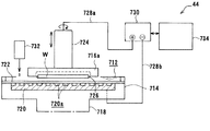
この研磨装置(電解研磨装置)44として、リン酸またはヒドロキシエタンビスホスホン酸のいずれかを含み砥粒を含まない研磨液を用いものを使用することが好ましい。この研磨装置(電解研磨装置)44の一例を図8に示す。
この研磨装置(電解研磨装置)44は、上方に開口して内部に研磨液712を保持する有底円筒状の電解槽714と、電解槽714の上方に配置され基板Wを着脱自在に下向きに保持する基板保持部716aとを有している。この研磨液712として、リン酸またはヒドロキシエタンビスホスホン酸のいずれかを含み砥粒を含まないものが用いられる。
As this polishing apparatus (electropolishing apparatus) 44, it is preferable to use a polishing liquid that contains either phosphoric acid or hydroxyethanebisphosphonic acid but does not contain abrasive grains. An example of this polishing apparatus (electropolishing apparatus) 44 is shown in FIG.
This polishing apparatus (electropolishing apparatus) 44 is open at the top and has a bottomed cylindrical
電解槽714は、モータ等の駆動に伴って回転する主軸718に直結され、底部には、例えばSUS,Pt/Ti,Ir/Ti,Ti,Ta,Nbなど研磨液に対して安定でかつ電解により不動体化しない金属からなり、研磨液712中に浸漬されてカソードとなる平板状の陰極板720が水平に配置されている。この陰極板720の上面には、縦及び横方向に面内の全長に亘って直線状に延びる格子状の長溝720aが設けられている。更に、陰極板720の上面には、例えば、連続発泡体式で不織布タイプの硬度研磨パッド(例えば:ロデールニッタ社 SUBA800)からなる研磨具722が貼り付けられている。この研磨具722は、必要に応じて備えられる。
The
これによって、主軸718の回転に伴って電解槽714が研磨具722と一体に回転し、研磨液712の供給に伴って研磨液712が長溝720aを通って流れ、しかも電解研磨に伴って生成される生成物や、水素ガス、酸素ガス等も長溝720aを通って基板Wと研磨具722の間から外方に排出される。
Accordingly, the
基板保持部716aは、回転速度が制御可能な回転機構と研磨圧力が調整可能な上下動機構を備えた支持ロッド724の下端に連結され、この下面に、例えば真空吸着方式で基板Wを吸着保持するようになっている。
The
基板保持部716aの下面外周部には、基板保持部716aで基板Wを吸着保持した時、基板Wの周縁部乃至ベベル部と接触して、基板Wの表面に成膜した配線材料(銅)をアノードにする電気接点726が設けられている。この電気接点726は、支持ロッド724に内蔵されたロール摺動コネクタおよび配線728aにより、外部に配置した電源としての整流器730の陽極端子へ結線され、前記陰極板720は、配線728bを介して整流器730の陰極端子に結線される。
A wiring material (copper) formed on the surface of the substrate W in contact with the peripheral edge or bevel of the substrate W when the substrate W is sucked and held by the
更に、電解槽714の上方に位置して、この内部に研磨液712を供給する研磨液供給ユニット732が配置され、更に各機器及び運転全般を調節し管理する制御ユニット734および安全装置(図示せず)などが備えられている。
Further, a polishing
この研磨装置(電解研磨装置)44にあっては、電解槽714内に、リン酸またはヒドロキシエタンビスホスホン酸のいずれかを含み砥粒を含まない研磨液712を供給し、この研磨液712が電解槽714をオーバフローする状態で、電解槽714と研磨具722を一体に回転させる。一方、配線材料(銅)を表面に成膜した基板Wを基板保持部716aで下向きに吸着保持しておく。この状態で、基板Wを前記電解槽714とは反対方向に回転させながら下降させ、この基板Wの表面(下面)を、必要に応じて、研磨具722の表面に接触させ、同時に、整流器730により陰極板720と電気接点726との間に電流を流す。すると、配線材料(銅)は、効果的に平坦化されながら研磨される。
In this polishing apparatus (electropolishing apparatus) 44, a polishing liquid 712 that contains either phosphoric acid or hydroxyethane bisphosphonic acid and does not contain abrasive grains is supplied into the
例えば、銅の不溶性錯体を形成する錯体形成剤と砥粒を含む研磨液を用いて、配線材料としての銅を電解研磨法で除去すると、配線表面に形成された銅の不溶性錯体を砥粒で研磨除去する際に、銅表面そのものにスクラッチなどのダメージを与える可能性がある。配線寸法が小さくなるにつれて、僅かなダメージであっても配線抵抗の増加に繋がるなど、例えば45nm以降の世代においては、平坦化後の配線表面のモフォロジー管理が重要になるとみられている。その場合には、砥粒を含まずに平坦化を実現できる電解研磨液が必要となる。リン酸またはヒドロキシエタンビスホスホン酸のような高粘性の酸を含み、砥粒を含まない研磨液を用いることで、このような要請に応えることができる。 For example, when copper as a wiring material is removed by an electrolytic polishing method using a polishing liquid containing a complex-forming agent that forms an insoluble complex of copper and abrasive grains, the insoluble complex of copper formed on the wiring surface is removed with abrasive grains. When removing by polishing, the copper surface itself may be damaged, such as scratches. For example, in the generation after 45 nm, it is considered that the management of the morphology of the wiring surface after flattening becomes important as the wiring size becomes smaller, even if a slight damage leads to an increase in wiring resistance. In that case, an electropolishing liquid capable of realizing flattening without containing abrasive grains is required. Such a demand can be met by using a polishing liquid that contains a highly viscous acid such as phosphoric acid or hydroxyethanebisphosphonic acid and does not contain abrasive grains.
導電膜兼密着膜除去装置46は、導電膜形成装置38で形成した配線用凹部内以外の余剰な導電膜及び密着膜形成装置36で形成した配線用凹部内以外の余剰な密着膜を連続して除去するためのものである。この例では、内部をN2ガス等の不活性ガス雰囲気に置換可能なプロセスチャンバ76とロードロック室78とを有する研磨装置からなる。この導電膜兼密着膜除去装置46は、薬液によるエッチング装置またはプラズマエッチング装置であってもよく、導電膜や密着膜の材料特性、前後の工程との整合性、あるいは除去後の表面モフォロジーなどを勘案して選択することができる。
The conductive film / adhesive
なお、密着膜を形成しない場合、導電膜兼密着膜除去装置46は、導電膜のみを除去する導電膜除去装置として機能する。また、この例では、単一の研磨装置(導電膜兼密着膜除去装置)46で導電膜と密着膜とを連続して除去するようにしているが、導電膜や密着膜の材料等に応じて、余剰な導電膜を除去する導電膜除去装置と、余剰な密着膜を除去する密着膜除去装置を個別に備えるようにしてもよい。更に、前述の余剰な配線材料(銅)を除去する研磨装置44で導電膜及び/または密着膜を除去するようにしてもよい。
When the adhesion film is not formed, the conductive film / adhesion
金属膜(保護膜)形成装置48は、余剰な配線材料(銅)を除去することで、基板の表面に露出した配線(銅配線)の表面に、CoWP合金膜等からなる金属膜(保護膜)を選択的に形成して、配線を保護するためのものである。この例では、内部をN2ガス等の不活性ガス雰囲気に置換可能なプロセスチャンバ80とロードロック室82とを有する無電解めっき装置からなる。そして、この無電解めっき装置(金属膜形成装置)48には、プロセスチャンバ80の内部に位置して、前処理槽、めっき処理槽及び後処理槽がそれぞれ備えられ、一連のめっき処理を連続して行うことができるようになっている。
The metal film (protective film) forming
なお、図示しないが、装置フレーム14内に、金属膜形成装置48で金属膜を選択的に形成した基板の表面に、SiN等からなる層間バリア膜を形成する層間バリア膜形成装置を配置してもよい。層間バリア膜形成装置は、例えばCVD装置、PVD装置または湿式めっき装置で構成される。
Although not shown, an interlayer barrier film forming apparatus for forming an interlayer barrier film made of SiN or the like is disposed in the
また、本装置のロード・アンロード室10の入口及び装置フレーム側出口には、一対のゲートバルブ16a,16bが備えられ、ロード・アンロード室12の入口及び装置フレーム側出口にも、一対のゲートバルブ18a,18bが備えられている。そして、ロード・アンロード室10,12には、不活性ガス供給ライン20及び排気ライン22がそれぞれ接続され、ロード・アンロード室10,12は、開閉弁を介して独自に給排気できるように構成されている。
In addition, a pair of
装置フレーム14は、密閉可能に構成されており、装置フレーム14には、不活性ガス供給源26から延び、途中に給気ポンプ28及び該ポンプ28を挟んで一対の開閉弁を介装した不活性ガス供給ライン30と、大気圧より高い所定の圧力で開く排気弁32を途中に介装した排気ライン34がそれそれぞれ接続されている。これにより、給気ポンプ28の作動に伴って、例えばN2ガス等の不活性ガスを装置フレーム14内に供給し、この装置フレーム14内の圧力が、大気圧より高い所定の圧力に達した時に、排気ライン34の排気弁32が開いて、装置フレーム14内を、大気圧より高い所定の圧力の不活性ガス雰囲気に維持できるようになっている。
The
このように、装置フレーム14の内部圧力を、大気圧より高い圧力(陽圧)に維持することで、不活性ガス雰囲気に置換した装置フレーム14内に大気が流入してしまうことを防止することができる。
以上のように装置フレーム14内を不活性ガス雰囲気にすることで、基板Wを上記の各装置間で搬送する際に大気に曝さずにすみ、配線形成途中の基板表面の酸化等を防ぐことができる。
In this way, by maintaining the internal pressure of the
By making the inside of the
次に、この配線形成装置による一連の配線形成処理を、図9乃至図16を更に参照して説明する。
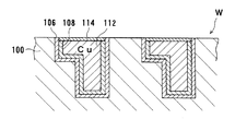
先ず、図10に示すように、例えばPVD、CVDまたは湿式塗布法でSiO2等からなる絶縁膜(層間絶縁膜)100を形成し、この絶縁膜100の内部に、例えばRIE、CDE、スパッタエッチングまたは湿式エッチングでトレンチ102及びビアホール104等の配線用凹部を有する配線パターンを形成した基板Wを用意し、この基板Wをカセット内に収納してロード・アンロード室10内に搬入する。同時に、空のカセットをロード・アンロード室12内に搬入する。これらの搬入後に、ロード・アンロード室10,12の内部をN2ガス等の不活性ガス雰囲気に置換する。
Next, a series of wiring forming processes by this wiring forming apparatus will be described with further reference to FIGS.
First, as shown in FIG. 10, an insulating film (interlayer insulating film) 100 made of SiO 2 or the like is formed by, for example, PVD, CVD, or wet coating method, and RIE, CDE, sputter etching, for example, is formed inside the insulating
つまり、ロード・アンロード室10,12の入口側のゲートバルブ16a,18aを開き、出口側のゲートバルブ16b,18bを開いた状態で、ロード・アンロード室10,12内にカセットを搬入し、しかる後、入口側のゲートバルブ16a,18aを閉じる。そして、ロード・アンロード室10,12の内部を、排気ライン22を通して排気するとともに、不活性ガス供給ライン20を通してN2ガス等の不活性ガスを供給して、ロード・アンロード室10,12の内部を、大気圧より高い圧力(陽圧)の不活性ガス雰囲気に置換する。
That is, the cassettes are loaded into the load / unload
装置フレーム14の内部にあっても同様に、排気ライン34を通して排気するとともに、不活性ガス供給ライン30を通してN2ガス等の不活性ガスを供給して、装置フレーム14の内部を、大気圧より高い圧力の不活性ガス雰囲気に置換する。この状態で、ロード・アンロード室10,12の装置フレーム14側出口のゲートバルブ16b,18bを開く。なお、ここでは配線形成前の基板Wをロード・アンロード室10から搬入し、配線形成後の基板Wをロード・アンロード室12から搬出する例を示しているが、一つのロード・アンロード室を利用し、あるカセットから基板Wを搬入して配線形成処理を行った後、配線が形成された基板Wを同一のカセットに戻すようにしてもよいことは勿論である。
Similarly, even inside the
次に、配線パターンを形成した基板Wを、搬送ロボット50で、ロード・アンロード室10内のカセットから一枚ずつ取出し、密着膜形成装置36の内部に搬入する。この密着膜形成装置36では、図11に示すように、絶縁膜100の表面に、スパッタリング等によって、タングステン、タンタルまたはチタンを含む密着膜106を形成する。
Next, the substrate W on which the wiring pattern is formed is taken out one by one from the cassette in the load / unload
この密着膜106を形成した基板Wを導電膜形成装置38内に搬入する。そして、この導電膜形成装置38で、図12に示すように、密着膜106の表面に、配線材料成膜用の電解めっき液に対して不溶性の、例えばパラジウム、ロジウムまたはルテニウムのいずれかを含む導電膜108を形成する。なお、前述のように、密着膜106は、これを介して、絶縁膜100と導電膜108との充分な密着性を確保するためのもので、絶縁膜100の表面に導電膜108を十分な密着性をもって形成できる場合には、密着膜を形成することなく、絶縁膜100の表面に導電膜108を直接形成するようにしてもよい。
The substrate W on which the
この導電膜108を形成した基板Wを電解めっき装置40内に搬入する。この電解めっき装置40では、導電膜108とアノード2−20との間に所定の電圧を印加しつつ、導電膜108を電解銅めっき液に接触させることで、図13に示すように、導電膜108の表面に、配線材料としての銅110を成膜して、トレンチ102及びビアホール104内への銅の埋込みを行う。そして、めっき後の基板Wを高速回転させてスピン乾燥させる。
The substrate W on which the
このように、配線材料成膜用の電解めっき液に対して不溶性の導電膜108を電解めっきのシード膜として使用して、この導電膜108の表面に配線材料(銅)110を直接成膜することで、薄い導電膜(シード膜)108であっても、導電膜108がめっき液に溶解することをなくして、導電膜108とめっき液とを十分に接触させてから成膜することが可能となる。これにより、導電膜108と十分な密着性を有する配線材料(銅)110を電解めっきによって導電膜108の全面に均一に形成して、信頼性の高い埋込み配線を再現性良く形成することができる。電解めっき装置40内の雰囲気は、大気でも不活性ガスでもよく、プロセスや装置全体の構成に応じて選べばよい。
As described above, the
そして、この銅110を形成した基板Wを、熱処理装置(ランプアニール装置)42内に搬入する。この熱処理装置42では、例えば、N2環境化で、基板Wに350℃で5分間の熱処理(ランプアニール)を施す。
Then, the substrate W on which the
このアニール後の基板Wを、研磨装置(電解研磨装置)44内に搬入する。この熱処理後の基板Wを膜厚測定器に搬送し、ここで銅の膜厚を測定し、この測定値によって、例えば次に基板に対するめっき時間を調整し、また膜厚が不足する場合には、再度めっきによる銅の追加の成膜を行うようにしてもよい。 The annealed substrate W is carried into a polishing apparatus (electropolishing apparatus) 44. The substrate W after the heat treatment is conveyed to a film thickness measuring device, where the film thickness of copper is measured, and the plating time for the substrate is then adjusted, for example, by this measured value. Further, additional film formation of copper by plating may be performed again.
この研磨装置44で、導電膜108の表面に成膜した不要な銅110、すなわちトレンチ102及びビアホール104内以外の銅110を除去する。導電膜108の表面に成膜した余剰の配線材料(銅)110を電解研磨で除去することにより、形成後の配線構造に対するダメージを最小とすることができる。この時、例えば、膜厚や基板の仕上がり具合をモニタで検査し、このモニタで終点(エンドポイント)を検知した時に、研磨を終了する。そして、この平坦化後の基板Wの表面を薬液で洗浄し、更に純水で洗浄(リンス)した後、高速回転させてスピン乾燥させる。
With this polishing
この不要な銅110を除去した基板Wを導電膜兼密着膜除去装置46内に搬入し、この導電膜兼密着膜除去装置46で、トレンチ102及びビアホール104内以外の余剰な導電膜108及び密着膜106を除去する。これによって、図14に示すように、絶縁膜100の内部に、銅からなる配線(銅配線)112を形成する。
なお、研磨装置44で導電膜108及び密着膜106も除去するようにすることで、配線材料(銅)100、導電膜108及び密着膜106の除去を研磨装置44で連続して行うことができる。
The substrate W from which the
The removal of the wiring material (copper) 100, the
この配線材料(銅)100、導電膜108及び密着膜106を除去した基板Wを金属膜形成装置(無電解めっき装置)48に搬送する。この金属膜形成装置48では、先ず前処理槽内で基板表面を前処理液に接触させ、これによって、配線112の表面の清浄化処理(CMP残渣除去処理)及びPd等の触媒を担持させる触媒担持処理等の前処理を行う。そして、前処理後の基板Wをめっき槽内に保持した、例えば80℃の無電解CoWPめっき液に3分間浸漬させ、しかる後、めっき後の基板Wの表面を後洗浄槽内で後洗浄液に接触させて基板Wの後洗浄等の後処理を行い、基板Wを高速で回転させてスピン乾燥させる一連の無電解めっき処理を施す。
The substrate W from which the wiring material (copper) 100, the
これにより、図15に示すように、絶縁膜100に形成した配線112の表面に、例えば膜厚が20nmのCoWPからなる金属膜(保護膜)114を選択的に形成して配線112を保護する。この金属膜114の膜厚は、0.1〜500nm、好ましくは、1〜200nm、更に好ましくは、10〜100nm程度である。この時、例えば、金属膜114の膜厚をモニタして、この膜厚が所定の値に達した時、つまり終点(エンドポイント)を検知した時に、無電解めっきを終了する。
As a result, as shown in FIG. 15, a metal film (protective film) 114 made of, for example, CoWP having a thickness of 20 nm is selectively formed on the surface of the
このように、配線112の表面のみに金属膜114を選択的に形成し、配線112の酸化防止、上層膜との密着性改善、上層の層間絶縁膜への配線材料の拡散防止などを図ることで、例えば45nm以降の世代において、配線間容量をより低下させたり、信頼性をより向上させたりすることができる。
As described above, the
そして、装置フレーム14内に層間バリア膜形成装置が備えられている場合には、この保護膜114を形成した基板Wを層間バリア膜形成装置に搬送し、この層間バリア膜形成装置で、図16に示すように、例えばCVDによって、基板Wの表面に、例えば30nm程度の膜厚のSiN等からなる層間バリア膜116を形成する。
そして、この層間バリア膜116を形成した基板Wを搬送ロボット50でロード・アンロード室12内のカセットに搬入する。
When the interlayer barrier film forming apparatus is provided in the
Then, the substrate W on which the
なお、上記の例では、配線材料として、銅を使用した例を示しているが、この銅の他に、銅合金、銀または銀合金を使用するようにしてもよい。また、保護膜114として、CoWP合金膜を使用した例を示しているが、CoWP合金の他に、Co単体やCoWB合金、CoP合金またはCoB等のCo合金を使用してもよく、更に、Ni単体や、NiWP合金、NiWB合金、NiP合金またはNiB合金等のNi合金を使用してもよい。
In the above example, copper is used as the wiring material. However, other than this copper, copper alloy, silver, or silver alloy may be used. In addition, although an example using a CoWP alloy film as the
10,12 ロード・アンロード室
14 装置フレーム
36 密着膜形成装置
38 導電膜形成装置
40 電解めっき装置装置
42 熱処理装置
44 研磨装置(電解研磨装置)
46 導電膜兼密着膜除去装置
48 金属膜形成装置
DESCRIPTION OF
46 conductive film and adhesion
Claims (18)
前記導電膜をシード膜として、電解めっき法により該導電膜の表面に配線材料を前記配線用凹部内に埋込みつつ成膜し、
前記導電膜の表面に成膜した余剰の配線材料を除去して前記配線用凹部内に埋込んだ配線材料で配線を形成することを特徴とする配線形成方法。 Forming a conductive film insoluble in the electrolytic plating solution for forming the wiring material on the surface of the substrate on which the wiring recesses are formed in the insulating film,
Using the conductive film as a seed film, an electroplating method is performed while embedding a wiring material on the surface of the conductive film in the wiring recess,
A wiring forming method comprising: removing a surplus wiring material formed on the surface of the conductive film, and forming a wiring with a wiring material embedded in the wiring recess.
前記導電膜に対して、前記電解めっき法による配線材料の成膜の前処理を施すことを特徴とする請求項1記載の配線形成方法。 After forming the insoluble conductive film,
The wiring formation method according to claim 1, wherein a pretreatment for forming a wiring material by the electrolytic plating method is performed on the conductive film.
前記密着膜の表面に配線材料成膜用の電解めっき液に対して不溶性の導電膜を形成し、
前記導電膜をシード膜として、電解めっき法により該導電膜の表面に配線材料を前記配線用凹部内に埋込みつつ成膜し、
前記導電膜の表面に成膜した余剰の配線材料を除去して前記配線用凹部内に埋込んだ配線材料で配線を形成することを特徴とする配線形成方法。 An adhesion film is formed on the surface of the substrate in which the recess for wiring is formed in the insulating film,
Forming an insoluble conductive film on the surface of the adhesion film with respect to the electrolytic plating solution for forming a wiring material;
Using the conductive film as a seed film, an electroplating method is performed while embedding a wiring material on the surface of the conductive film in the wiring recess,
A wiring forming method comprising: removing a surplus wiring material formed on the surface of the conductive film, and forming a wiring with a wiring material embedded in the wiring recess.
前記導電膜に対して、前記電解めっき法による配線材料の成膜の前処理を施すことを特徴とする請求項4記載の配線形成方法。 After forming the insoluble conductive film,
The wiring formation method according to claim 4, wherein a pretreatment for forming a wiring material by the electrolytic plating method is performed on the conductive film.
前記導電膜の表面に配線材料を成膜する電解めっき装置と、
前記導電膜の表面に成膜した余剰の配線材料を除去する研磨装置を有することを特徴とする配線形成装置。 A conductive film forming apparatus for forming a conductive film insoluble in an electrolytic plating solution for forming a wiring material on the surface of a substrate having a wiring recess;
An electroplating apparatus for forming a wiring material on the surface of the conductive film;
A wiring forming apparatus comprising a polishing apparatus that removes excess wiring material formed on the surface of the conductive film.
Priority Applications (2)
| Application Number | Priority Date | Filing Date | Title |
|---|---|---|---|
| JP2004307354A JP2006120870A (en) | 2004-10-21 | 2004-10-21 | Wire formation method and device thereof |
| US11/254,789 US20060086618A1 (en) | 2004-10-21 | 2005-10-21 | Method and apparatus for forming interconnects |
Applications Claiming Priority (1)
| Application Number | Priority Date | Filing Date | Title |
|---|---|---|---|
| JP2004307354A JP2006120870A (en) | 2004-10-21 | 2004-10-21 | Wire formation method and device thereof |
Publications (2)
| Publication Number | Publication Date |
|---|---|
| JP2006120870A true JP2006120870A (en) | 2006-05-11 |
| JP2006120870A5 JP2006120870A5 (en) | 2007-07-19 |
Family
ID=36205204
Family Applications (1)
| Application Number | Title | Priority Date | Filing Date |
|---|---|---|---|
| JP2004307354A Pending JP2006120870A (en) | 2004-10-21 | 2004-10-21 | Wire formation method and device thereof |
Country Status (2)
| Country | Link |
|---|---|
| US (1) | US20060086618A1 (en) |
| JP (1) | JP2006120870A (en) |
Cited By (5)
| Publication number | Priority date | Publication date | Assignee | Title |
|---|---|---|---|---|
| JP2009064803A (en) * | 2007-09-04 | 2009-03-26 | Renesas Technology Corp | Semiconductor device |
| JP2010512002A (en) * | 2006-11-30 | 2010-04-15 | アドバンスト・マイクロ・ディバイシズ・インコーポレイテッド | Semiconductor structure having wiring containing silver and method of forming the same |
| JP2011523780A (en) * | 2008-05-21 | 2011-08-18 | インターナショナル・ビジネス・マシーンズ・コーポレーション | Structure and process for the incorporation of conductive contacts |
| US8198730B2 (en) | 2007-01-10 | 2012-06-12 | Nec Corporation | Semiconductor device and method of manufacturing the same |
| KR101458038B1 (en) * | 2006-11-30 | 2014-11-03 | 글로벌파운드리즈 인크. | Semiconductor structure with interconnect comprising silver and mehod of forming the same |
Families Citing this family (4)
| Publication number | Priority date | Publication date | Assignee | Title |
|---|---|---|---|---|
| EP2381008A2 (en) * | 2006-08-28 | 2011-10-26 | Osaka University | Catalyst-aided chemical processing method and apparatus |
| JP2008141088A (en) * | 2006-12-05 | 2008-06-19 | Nec Electronics Corp | Method for manufacturing semiconductor device |
| WO2011115878A1 (en) * | 2010-03-19 | 2011-09-22 | Sigma-Aldrich Co. | Methods for preparing thin fillms by atomic layer deposition using hydrazines |
| TW202138115A (en) * | 2019-12-24 | 2021-10-16 | 日商荏原製作所股份有限公司 | Substrate processing apparatus, substrate processing method, and substrate processing system |
Family Cites Families (5)
| Publication number | Priority date | Publication date | Assignee | Title |
|---|---|---|---|---|
| EP1204139A4 (en) * | 2000-04-27 | 2010-04-28 | Ebara Corp | Rotation holding device and semiconductor substrate processing device |
| JP4644926B2 (en) * | 2000-10-13 | 2011-03-09 | ソニー株式会社 | Semiconductor manufacturing apparatus and semiconductor device manufacturing method |
| JP3664669B2 (en) * | 2001-06-27 | 2005-06-29 | 株式会社荏原製作所 | Electrolytic plating equipment |
| AU2003217197A1 (en) * | 2002-01-10 | 2003-07-30 | Semitool, Inc. | Method for applying metal features onto barrier layers using electrochemical deposition |
| US7223685B2 (en) * | 2003-06-23 | 2007-05-29 | Intel Corporation | Damascene fabrication with electrochemical layer removal |
-
2004
- 2004-10-21 JP JP2004307354A patent/JP2006120870A/en active Pending
-
2005
- 2005-10-21 US US11/254,789 patent/US20060086618A1/en not_active Abandoned
Cited By (5)
| Publication number | Priority date | Publication date | Assignee | Title |
|---|---|---|---|---|
| JP2010512002A (en) * | 2006-11-30 | 2010-04-15 | アドバンスト・マイクロ・ディバイシズ・インコーポレイテッド | Semiconductor structure having wiring containing silver and method of forming the same |
| KR101458038B1 (en) * | 2006-11-30 | 2014-11-03 | 글로벌파운드리즈 인크. | Semiconductor structure with interconnect comprising silver and mehod of forming the same |
| US8198730B2 (en) | 2007-01-10 | 2012-06-12 | Nec Corporation | Semiconductor device and method of manufacturing the same |
| JP2009064803A (en) * | 2007-09-04 | 2009-03-26 | Renesas Technology Corp | Semiconductor device |
| JP2011523780A (en) * | 2008-05-21 | 2011-08-18 | インターナショナル・ビジネス・マシーンズ・コーポレーション | Structure and process for the incorporation of conductive contacts |
Also Published As
| Publication number | Publication date |
|---|---|
| US20060086618A1 (en) | 2006-04-27 |
Similar Documents
| Publication | Publication Date | Title |
|---|---|---|
| TW567580B (en) | Semiconductor manufacturing device and manufacturing method for semiconductor device | |
| US6717189B2 (en) | Electroless plating liquid and semiconductor device | |
| JP3979464B2 (en) | Electroless plating pretreatment apparatus and method | |
| US7141274B2 (en) | Substrate processing apparatus and method | |
| US20040234696A1 (en) | Plating device and method | |
| US6706422B2 (en) | Electroless Ni—B plating liquid, electronic device and method for manufacturing the same | |
| US20060086618A1 (en) | Method and apparatus for forming interconnects | |
| US7947156B2 (en) | Substrate processing apparatus and substrate processing method | |
| EP1430167A2 (en) | Plating apparatus and method | |
| US20040235237A1 (en) | Semiconductor device and method for manufacturing the same | |
| KR100891344B1 (en) | Electroless-plating solution and semiconductor device | |
| US20040170766A1 (en) | Electroless plating method and device, and substrate processing method and apparatus | |
| JP4064132B2 (en) | Substrate processing apparatus and substrate processing method | |
| JP3812891B2 (en) | Wiring formation method | |
| JP2002285343A (en) | Electroless plating apparatus | |
| JP4139124B2 (en) | Plating apparatus and method | |
| JP2010007153A (en) | Plating apparatus and plating method | |
| JP2004300576A (en) | Method and apparatus for substrate treatment | |
| JP4060700B2 (en) | Substrate processing apparatus and substrate processing method | |
| WO2002092877A2 (en) | Catalyst-imparting treatment solution and electroless plating method | |
| JP2005116630A (en) | Wiring forming method and apparatus thereof | |
| JP2003183892A (en) | Plating apparatus | |
| JP3886383B2 (en) | Plating apparatus and plating method | |
| JP2008150631A (en) | Plating apparatus and plating method | |
| JP2003034876A (en) | Catalytic treatment liquid and method for electroless plating |
Legal Events
| Date | Code | Title | Description |
|---|---|---|---|
| A521 | Request for written amendment filed |
Free format text: JAPANESE INTERMEDIATE CODE: A523 Effective date: 20070606 |
|
| A621 | Written request for application examination |
Free format text: JAPANESE INTERMEDIATE CODE: A621 Effective date: 20070606 |
|
| A977 | Report on retrieval |
Free format text: JAPANESE INTERMEDIATE CODE: A971007 Effective date: 20090810 |
|
| A131 | Notification of reasons for refusal |
Free format text: JAPANESE INTERMEDIATE CODE: A131 Effective date: 20090818 |
|
| A02 | Decision of refusal |
Free format text: JAPANESE INTERMEDIATE CODE: A02 Effective date: 20100105 |