JP2006085754A - Driving device for laser diode - Google Patents
Driving device for laser diode Download PDFInfo
- Publication number
- JP2006085754A JP2006085754A JP2004266522A JP2004266522A JP2006085754A JP 2006085754 A JP2006085754 A JP 2006085754A JP 2004266522 A JP2004266522 A JP 2004266522A JP 2004266522 A JP2004266522 A JP 2004266522A JP 2006085754 A JP2006085754 A JP 2006085754A
- Authority
- JP
- Japan
- Prior art keywords
- voltage
- laser diode
- circuit
- drive
- driving
- Prior art date
- Legal status (The legal status is an assumption and is not a legal conclusion. Google has not performed a legal analysis and makes no representation as to the accuracy of the status listed.)
- Granted
Links
Images


Abstract
Description
本発明は、光記録媒体にレーザビームを照射するレーザダイオードを駆動する駆動装置に関する。 The present invention relates to a driving device that drives a laser diode that irradiates an optical recording medium with a laser beam.
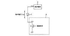
レーザダイオードを駆動する従来装置としては図1に示す如き構成が一般的である。図1の駆動装置においては、レーザダイオード1のアノードには固定電源2から一定電圧Vccが印加され、レーザダイオード1のカソードは駆動トランジスタ3のコレクタに接続されている。駆動トランジスタ3は、駆動IC4内に備えられており、ベースに駆動信号が供給されるとそのコレクタ・エミッタ間がオンとなり、レーザダイオード1に駆動電流が流れるのでレーザダイオード1は発光することになる。
As a conventional device for driving a laser diode, a configuration as shown in FIG. 1 is common. In the driving apparatus of FIG. 1, a constant voltage Vcc is applied from the
かかる従来の駆動装置においては、レーザダイオード1に流れる駆動電流量やそれ自体の温度によってレーザダイオード1の動作電圧Vopが増減する。駆動電流が大きいとVopは高くなり、温度が下がるとVopは高くなる。 In such a conventional driving device, the operating voltage Vop of the laser diode 1 increases or decreases depending on the amount of driving current flowing through the laser diode 1 and the temperature of itself. When the drive current is large, Vop increases, and when the temperature decreases, Vop increases.
レーザダイオード1の温度が高くなると、図2に示すように、レーザダイオード1の動作電圧Vopが低くなり、そのとき、光パワーを高く設定しようとして駆動電流量を大きくした場合、駆動トランジスタ3のコレクタ電圧Vcが上昇し、図3に示すように、駆動IC4の消費電力が増加するので、駆動IC4の発熱量が増加して動作が不安定になる。 When the temperature of the laser diode 1 is increased, as shown in FIG. 2, the operating voltage Vop of the laser diode 1 is lowered. At this time, if the drive current amount is increased in order to set the optical power high, the collector of the drive transistor 3 As the voltage Vc rises and the power consumption of the drive IC 4 increases as shown in FIG. 3, the amount of heat generated by the drive IC 4 increases and the operation becomes unstable.
一方、レーザダイオード1の温度が低くなると、レーザダイオード1の動作電圧Vopが上昇し、駆動トランジスタ3のコレクタ電圧Vcが低下し、閾値電圧以下になると駆動トランジスタ3が飽和状態となり、その動作が非線形となって書き込み波形が歪むことにより、光出力波形のスルーレートが劣化する。 On the other hand, when the temperature of the laser diode 1 is lowered, the operating voltage Vop of the laser diode 1 is increased, the collector voltage Vc of the driving transistor 3 is decreased, and when the temperature is lower than the threshold voltage, the driving transistor 3 is saturated and its operation is nonlinear. As a result, the write waveform is distorted, so that the slew rate of the optical output waveform is degraded.
本発明が解決しようとする課題には、上記の欠点が一例として挙げられ、レーザダイオードに対する駆動動作の安定化を図り、光出力波形のスルーレートを改善することができる駆動装置を提供することが本発明の目的である。 The problems to be solved by the present invention include the above-mentioned drawbacks as an example, and it is possible to provide a driving device capable of stabilizing the driving operation for the laser diode and improving the slew rate of the optical output waveform. It is an object of the present invention.
請求項1に係る発明の駆動装置は、光記録媒体にレーザビームを照射するレーザダイオードを駆動する駆動装置であって、前記レーザダイオードと直列に接続されて駆動信号に応じて前記レーザダイオードに電流を流す駆動回路と、前記レーザダイオードと前記駆動回路との直列回路に直流電圧を印加する直流電源と、前記レーザダイオードと前記駆動回路との接続点の電圧を検出する電圧検出手段と、前記電圧検出手段によって検出された電圧に応じて前記直流電源による前記直列回路への印加電圧を変化させる制御手段と、を備えたことを特徴としている。 According to a first aspect of the present invention, there is provided a driving device for driving a laser diode for irradiating an optical recording medium with a laser beam, wherein the driving device is connected in series with the laser diode and a current is supplied to the laser diode in accordance with a driving signal. A drive circuit for supplying a current, a DC power supply for applying a DC voltage to a series circuit of the laser diode and the drive circuit, a voltage detection means for detecting a voltage at a connection point between the laser diode and the drive circuit, and the voltage And control means for changing the voltage applied to the series circuit by the DC power supply in accordance with the voltage detected by the detection means.
請求項7に係る発明の駆動装置は、光記録媒体にレーザビームを照射するレーザダイオードを駆動する駆動装置であって、前記レーザダイオードと直列に接続されて駆動信号に応じて前記レーザダイオードに電流を流す駆動回路と、前記レーザダイオードと前記駆動回路との直列回路に直流電圧を印加する直流電源と、前記レーザダイオードの温度を検出する温度検出手段と、前記温度検出手段によって検出された温度に応じて前記直流電源による前記直列回路への印加電圧を変化させる制御手段と、を備えたことを特徴としている。 According to a seventh aspect of the present invention, there is provided a driving device for driving a laser diode for irradiating an optical recording medium with a laser beam, wherein the driving device is connected in series with the laser diode and a current is supplied to the laser diode in accordance with a driving signal. A driving circuit for supplying a current, a DC power source for applying a DC voltage to a series circuit of the laser diode and the driving circuit, a temperature detecting means for detecting the temperature of the laser diode, and a temperature detected by the temperature detecting means. And a control means for changing a voltage applied to the series circuit by the DC power supply.
以下、本発明の実施例を図面を参照しつつ詳細に説明する。 Hereinafter, embodiments of the present invention will be described in detail with reference to the drawings.
図4は本発明によるレーザダイオードの駆動装置を示しており、駆動装置はディスク記録再生装置の一部として備えられている。この駆動装置では、レーザダイオード11を駆動するために可変電源12及び駆動IC13が備えられている。可変電源12は直流電圧を出力し、駆動IC13から出力される電圧制御信号に応じてその出力電圧Vvarを変化する。可変電源12の出力電圧Vvarはレーザダイオード11のアノードに印加される。駆動IC13は駆動トランジスタ15及び電圧検出制御回路16を有している。駆動回路としての駆動トランジスタ15のコレクタがレーザダイオード11のカソード及び電圧検出制御回路16の入力に接続されている。駆動トランジスタ15のコレクタ電圧が電圧検出制御回路16に供給される。
FIG. 4 shows a laser diode driving apparatus according to the present invention, and the driving apparatus is provided as a part of a disk recording / reproducing apparatus. In this driving apparatus, a
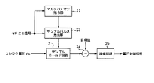
電圧検出制御回路16は、図5に示すように、サンプルホールド回路21、マルチパルスオフ指令部22、サンプルパルス発生器23、減算器24及び増幅回路25からなる。サンプルホールド回路21は、駆動トランジスタ15のコレクタ電圧をサンプルパルス発生器22から供給されるサンプルパルスに応じて検出して値として保持する。マルチパルスオフ指令部22及びサンプルパルス発生器23には記録信号であるNRZI信号が供給される。マルチパルスオフ指令部22はNRZI信号が光ディスク上の規定区間としてのAPC(オートパワーコントロール)エリアへの記録信号であることを判断するためにNRZI信号に応じて特定のラン長時を検出し、その特定のラン長時にマルチパルスオフを指令するマルチパルスオフ指令信号を発生する。また、マルチパルスオフ指令部22はディスク上のAPCエリアを検出しても良い。APCエリアは書込内容に制限がないエリアである。
As shown in FIG. 5, the voltage
サンプルパルス発生器23は、NRZI信号及びマルチパルスオフ指令信号に応じてサンプルパルスを発生する。減算器24はサンプルホールド回路21によって保持されたコレクタ電圧値と目標値との差を算出して差信号として増幅回路25に供給する。増幅回路25は差信号を増幅して電圧制御信号として可変電源12に供給する。
The
ディスク記録再生装置においては、図6に示すように、ピックアップ装置31は上記のレーザダイオード11及び駆動IC13を備えている。ピックアップ装置31は更にフロントモニタ32、光検出器33及び温度センサ34を備えている。フロントモニタ32はレーザダイオード11の発光強度を検出するために備えられている。光検出器33はディスクからの反射光を受光して読取信号を生成する。温度センサ34はレーザダイオード11の温度を検出する。
In the disk recording / reproducing apparatus, as shown in FIG. 6, the
記録制御回路35はNRZI信号をピックアップ装置31の駆動IC13に出力する。また、記録制御回路35は記録時にはそれを示す信号をAPC回路36及び可変電源12に供給する。APC回路36は記録時と再生時とで異なる発光強度を得るようにフロントモニタ32による検出強度に応じて強度制御信号を駆動IC13に出力する。
The
光検出器33の出力には再生処理回路37が接続されている。再生処理回路37は光検出器33からの読取信号を復調して再生信号を生成する。また、光検出器33からの読取信号はAPCエリア検出器38及びサーボ回路39に供給される。APCエリア検出器38は読取信号に応じてピックアップ装置による記録又は再生位置、すなわちレーザビームの照射位置がディスク上のAPCエリアであることを検出する。サーボ回路39は読取信号に応じてフォーカスエラー信号、トラッキングエラー信号等のサーボ信号を生成してドライバ40に供給する。ドライバ40はそのサーボ信号に応じてピックアップ装置のフォーカス及びトラッキング用を含む各種アクチュエータ(図示せず)を駆動する。
A
可変電源12、記録制御回路35、APC回路36、再生処理回路37、APCエリア検出器38及びサーボ回路39はCPU(中央演算装置)41によって制御される。CPU41には温度センサ34の出力信号が供給され、CPU41は温度センサ34によって検出されたレーザダイオード11の温度に応じて可変電源12の出力電圧Vvarを制御する。
The
かかる構成のディスク記録再生装置においてレーザダイオードの駆動装置の駆動電圧制御を次に説明する。駆動電圧制御においてはサンプルパルスのタイミングに同期して図7に示すように、先ず、ディスク記録再生装置が記録時であるか否かがCPU41によって判別される(ステップS1)。記録時はレーザダイオード11から発射された書込用レーザビーム(ライトマルチパルス及びイレースマルチパルスを含む)が光ディスクに照射されるときである。記録時であれば、APCエリア検出器38が作動し(ステップS2)、記録位置がディスク上のAPCエリアであるか否かがAPCエリア検出器38の検出出力に応じて記録制御回路35において判別される(ステップS3)。光ディスクは図8に示すように、内周側から外周側に向けてAPCエリア、同期エリア、ユーザデータエリア及びリンクエリアからなるデータ構造を有している。ステップS3の判別結果がAPCエリアであるならば、電圧検出制御回路16によるコレクタ電圧検出が行われる(ステップS4)。すなわち、マルチパルスオフ指令部22がライトマルチパスオフ指令を発生し、ライトマルチパスオフ指令に応答してサンプルパルス発生器23からサンプルホールド回路21に対してサンプルパルスが供給されるので、サンプルホールド回路21は駆動トランジスタ15のコレクタ電圧の値をそのサンプルパルスに応じて読み取って保持する。保持されたコレクタ電圧の値は記録時の目標値との差が減算器24によって算出され、その差は増幅回路25によって増幅されて電圧制御信号として可変電源12に供給される(ステップS5)。
Next, driving voltage control of the laser diode driving device in the disk recording / reproducing apparatus having such a configuration will be described. In the drive voltage control, as shown in FIG. 7, in synchronization with the timing of the sample pulse, first, the
ステップS3の判別結果がAPCエリア以外であるならば、記録制御回路35は可変電源12に現在の出力電圧Vvarを維持させる(ステップS6)。
If the determination result in step S3 is outside the APC area, the
一方、ステップS1において記録時ではないならば、レーザダイオード11から発射された読取用レーザビームが光ディスクに照射される再生時である。再生時には、サンプルパルス発生器23からサンプルホールド回路21に対してサンプルパルスが供給されるので、サンプルホールド回路21は駆動トランジスタ15のコレクタ電圧の値をそのサンプルパルスに応じて読み取って保持する(ステップS7)。保持されたコレクタ電圧の値は再生時の目標値との差が減算器24によって算出され、その差は増幅回路25によって増幅されて電圧制御信号として可変電源12に供給される(ステップS8)。
On the other hand, if it is not at the time of recording in step S1, it is at the time of reproduction in which the reading laser beam emitted from the
かかる駆動動作によって、サンプルホールド回路21の保持電圧と目標値との差が減少するように可変電源12の出力電圧Vvarが制御される。保持電圧が低ければ、コレクタ電圧Vcが低下し飽和の危険性がある。この場合には、電圧制御信号の電圧が高くなるので可変電源12の出力電圧Vvarが高くなり、コレクタ電圧Vcの低下を防止するようにネガティブフィードバック制御として動作する。よって、コレクタ電圧Vcは適正値に維持されるので、トランジスタの飽和が防止され、結果として、光出力のスルーレート劣化を防止することができる。
With this driving operation, the output voltage Vvar of the
一方、目標値に対して保持電圧が高ければ、コレクタ電圧Vcが必要以上に上昇して消費電力の増加による駆動トランジスタ15の発熱の危険性がある。この場合には、電圧制御信号の電圧が低くなるので可変電源12の出力電圧Vvarを低くなり、コレクタ電圧Vcの上昇を防止するようにネガティブフィードバック制御として動作する。したがってコレクタ電圧Vcは適正値に維持され、駆動トランジスタ15の消費電力の増加を防止することができ、結果として、駆動トランジスタ15の発熱による誤動作を防止することができる。
On the other hand, if the holding voltage is higher than the target value, the collector voltage Vc rises more than necessary and there is a risk of heat generation of the
図9〜図11はかかる駆動装置によるレーザビームの光パワー、ライトマルチパルスオフ指令及びサンプルパルス各々の関係を示している。図9においては記録時にAPCエリアではマルチパルスオフ指令信号に応答してライト(書込)マルチパルスを停止させた場合を示している。また、イレースマルチパルスも停止されてそのピーク値に保持させている。その停止時に光パワーをライトマルチパルスのピーク値に保持させ、そのときにサンプルパルスが生成され、駆動トランジスタ15のコレクタ電圧が検出される。図10においては記録時にAPCエリアではマルチパルスオフ指令信号に応答してライトマルチパルスを停止させると共にイレース(消去)パワーをライトピーク値にした場合を示している。ライトピーク値にしたときにサンプルパルスが生成され、駆動トランジスタ15のコレクタ電圧が検出される。図11においては記録時にAPCエリアではイレースマルチパルスを停止させて光パワーをイレースピーク値にしてそのイレースピーク値にあるときにサンプルパルスを生成した場合を示している。また、図12においては記録時にイレースマルチパルスが生成されない場合を示し、この場合にはAPCエリアとは無関係に光パワーがイレースピーク値にあるときにサンプルパルスが生成される。図11及び図12の場合には、電圧検出制御回路16はイレースパワー時のコレクタ電圧値をサンプルパルスに応じて保持し、ライトパワー時のコレクタ電圧値を推測してそれを検出電圧として電圧制御信号を生成する。
9 to 11 show the relationship between the optical power of the laser beam, the write multi-pulse off command, and the sample pulse by the driving device. FIG. 9 shows a case where the write (write) multi-pulse is stopped in response to the multi-pulse off command signal in the APC area during recording. The erase multi-pulse is also stopped and held at its peak value. At that time, the optical power is held at the peak value of the write multi-pulse, and at that time, a sample pulse is generated and the collector voltage of the
図13は電圧検出制御回路16の他の回路例を示している。図13の電圧検出制御回路16はボトムホールド回路26、減算器27及び増幅回路28からなる。
FIG. 13 shows another circuit example of the voltage
ライトマルチパルスがピークの光パワーを出射しているときにはレーザダイオード11には最大電流が流れ、駆動トランジスタ15の動作電圧Vopは最大となり、駆動トランジスタ15のコレクタ電圧Vcは最小となる。この最小電圧、すなわちボトム電圧はボトムホールド回路26によって保持される。保持電圧は減算器27によって目標値と比較され、減算器27からは保持電圧と目標値との差が信号として出力される。その差は増幅回路28によって増幅されて電圧制御信号として可変電源12に供給される。これにより、保持電圧と目標値との差が減少するように可変電源12の出力電圧Vvarが制御される。保持電圧が低ければ、コレクタ電圧Vcが低下し飽和の危険性がある。この場合には、電圧制御信号の電圧が高くなるので可変電源12の出力電圧Vvarが高くなり、コレクタ電圧Vcの低下を防止するようにネガティブフィードバック制御として動作する。よって、コレクタ電圧Vcは適正値に維持されるので、トランジスタの飽和が防止され、結果として、光出力のスルーレート劣化を防止することができる。
When the light multipulse emits the peak optical power, the maximum current flows through the
一方、目標値に対して保持電圧が高ければ、コレクタ電圧Vcが必要以上に上昇して消費電力の増加による駆動トランジスタ15の発熱の危険性がある。この場合には、電圧制御信号の電圧が低くなるので可変電源12の出力電圧Vvarを低くなり、コレクタ電圧Vcの上昇を防止するようにネガティブフィードバック制御として動作する。したがってコレクタ電圧Vcは適正値に維持され、駆動トランジスタ15の消費電力の増加を防止することができ、結果として、駆動トランジスタ15の発熱による誤動作を防止することができる。
On the other hand, if the holding voltage is higher than the target value, the collector voltage Vc rises more than necessary and there is a risk of heat generation of the
図14は本発明の他の実施例を示している。図14のレーザダイオードの駆動装置においては、駆動IC13は駆動トランジスタ15としてPNP型のものが用いられている。よって、レーザダイオード11を駆動するために可変電源12及び駆動IC13が備えられている。可変電源12の出力電圧Vvarは駆動トランジスタ15のエミッタに印加される。駆動トランジスタ15のコレクタがレーザダイオード11のアノード及び電圧検出制御回路16の入力に接続されている。駆動トランジスタ15のコレクタ電圧が電圧検出制御回路16に供給される。レーザダイオード11のカソードは直接アース接続されている。
FIG. 14 shows another embodiment of the present invention. In the laser diode driving apparatus of FIG. 14, the driving
図14のレーザダイオードの駆動装置をディスク記録再生装置に適用した場合においても上記の図4のレーザダイオードの駆動装置と同様に動作するので、ここでの詳細な説明は省略する。 Even when the laser diode driving apparatus of FIG. 14 is applied to a disk recording / reproducing apparatus, it operates in the same manner as the laser diode driving apparatus of FIG. 4 described above, and a detailed description thereof will be omitted.
図2に示したように、レーザダイオードの温度によってレーザダイオードの動作電圧が増減するので、温度センサ34の出力に応じて可変電源12の出力電圧Vvarを制御しても良い。この制御を行うと、駆動トランジスタ16のコレクタ電圧Vcの動作電圧を温度変化があっても維持することができる。具体的には、図15に示す特性のように、レーザダイオードの温度上昇に従って可変電源の出力電圧Vvarを低下させることが行われる。
As shown in FIG. 2, since the operating voltage of the laser diode increases or decreases depending on the temperature of the laser diode, the output voltage Vvar of the
レーザダイオードの温度変化に対応した駆動電圧制御においては、図16に示すように、先ず、ディスク記録再生装置が記録時であるか否かがCPU41によって判別される(ステップS11)。記録時であれば、温度センサ34の出力に応じてレーザダイオード11の温度が低温(例えば、5度以下)であるか否かが判別される(ステップS12)。低温であるならば、CPU41は可変電源12の出力電圧Vvarを第1所定電圧V1(例えば、9V)に設定させる(ステップS13)。低温ではないならば、CPU41は可変電源12の出力電圧Vvarを第1所定電圧V1より低い第2所定電圧V2(例えば、8V)に設定させる(ステップS14)。
In the drive voltage control corresponding to the temperature change of the laser diode, as shown in FIG. 16, first, the
一方、ステップS11の判別により記録時ではない場合、すなわち再生時である場合には、温度センサ34の出力に応じてレーザダイオード11の温度が低温であるか否かが判別される(ステップS15)。低温であるならば、CPU41は可変電源12の出力電圧Vvarを第2所定電圧V2より低い第3所定電圧V3(例えば、7V)に設定させる(ステップS16)。低温ではないならば、CPU41は可変電源12の出力電圧Vvarを第3所定電圧V3より低い第4所定電圧V4(例えば、6V)に設定させる(ステップS17)。
On the other hand, if it is not at the time of recording, that is, at the time of reproduction by the determination in step S11, it is determined whether or not the temperature of the
かかる駆動電圧制御においては、記録時及び再生時各々でレーザダイオード11の温度に応じて可変電源12の出力電圧Vvarを制御することが行われる。記録時には可変電源12の出力電圧Vvarを再生時よりも高く設定するので、記録のために最適な光パワーを得ることができる。また、再生時には駆動トランジスタの電力消費を抑えることができる。
In such drive voltage control, the output voltage Vvar of the
また、本発明の他の実施例として、記録時にレーザダイオード11に流すべき電流設定値に応じて可変電源12の出力電圧Vvarを制御するようにしても良い。例えば、図17に示すように、駆動装置には記録時にレーザダイオード11に流すべき記録電流値を設定する記録電流設定回路41が備えられ、記録電流設定回路41から得られる記録電流設定値に応じて演算装置42は可変電源12の出力電圧Vvarを指定する。可変電源12の出力電圧Vvarは記録電流設定値に応じて図18に示す特性の如く設定される。すなわち、記録電流設定値が高くなるに従って可変電源12の出力電圧Vvarが高くなる。更に、図17に示すように、記録電流設定値だけでなく温度センサ34の出力信号に応じて可変電源12の出力電圧Vvarを設定しても良い。また、レーザダイオード11の駆動電流の実際の計測値に応じて可変電源12の出力電圧Vvarを制御するようにしても良い。
As another embodiment of the present invention, the output voltage Vvar of the
以上のように、本発明によれば、レーザダイオードと直列に接続されて駆動信号に応じてレーザダイオードに電流を流す駆動回路と、レーザダイオードと駆動回路との直列回路に直流電圧を印加する直流電源とを備え、電圧検出手段によって検出されたレーザダイオードと駆動回路との接続点の電圧に応じて直流電源による直列回路への印加電圧が変化される。また、本発明によれば、温度検出手段によって検出された温度に応じて直流電源による直列回路への印加電圧が変化される。よって、直流電源による直列回路への印加電圧を適切に制御することができるので、レーザダイオードに対する駆動動作の安定化を図り、光出力波形のスルーレートを改善することができる。 As described above, according to the present invention, a drive circuit that is connected in series with the laser diode and supplies a current to the laser diode in response to the drive signal, and a direct current that applies a DC voltage to the series circuit of the laser diode and the drive circuit. The voltage applied to the series circuit by the DC power supply is changed according to the voltage at the connection point between the laser diode and the drive circuit detected by the voltage detection means. Further, according to the present invention, the voltage applied to the series circuit by the DC power supply is changed according to the temperature detected by the temperature detecting means. Therefore, the voltage applied to the series circuit by the DC power supply can be appropriately controlled, so that the driving operation for the laser diode can be stabilized and the slew rate of the optical output waveform can be improved.
1,11 レーザダイオード
3,15 駆動トランジスタ
4,13 駆動IC
12 可変電源
16 電流検出制御回路
1,11
12
Claims (10)
前記レーザダイオードと直列に接続されて駆動信号に応じて前記レーザダイオードに電流を流す駆動回路と、
前記レーザダイオードと前記駆動回路との直列回路に直流電圧を印加する直流電源と、
前記レーザダイオードと前記駆動回路との接続点の電圧を検出する電圧検出手段と、
前記電圧検出手段によって検出された電圧に応じて前記直流電源による前記直列回路への印加電圧を変化させる制御手段と、を備えたことを特徴とする駆動装置。 A driving device for driving a laser diode that irradiates a laser beam onto an optical recording medium,
A drive circuit connected in series with the laser diode and causing a current to flow through the laser diode in response to a drive signal;
A DC power supply for applying a DC voltage to a series circuit of the laser diode and the drive circuit;
Voltage detection means for detecting a voltage at a connection point between the laser diode and the drive circuit;
And a control means for changing a voltage applied to the series circuit by the DC power supply in accordance with a voltage detected by the voltage detection means.
前記レーザダイオードと直列に接続されて駆動信号に応じて前記レーザダイオードに電流を流す駆動回路と、
前記レーザダイオードと前記駆動回路との直列回路に直流電圧を印加する直流電源と、
前記レーザダイオードの温度を検出する温度検出手段と、
前記温度検出手段によって検出された温度に応じて前記直流電源による前記直列回路への印加電圧を変化させる制御手段と、を備えたことを特徴とする駆動装置。 A driving device for driving a laser diode that irradiates a laser beam onto an optical recording medium,
A drive circuit connected in series with the laser diode and causing a current to flow through the laser diode in response to a drive signal;
A DC power supply for applying a DC voltage to a series circuit of the laser diode and the drive circuit;
Temperature detecting means for detecting the temperature of the laser diode;
And a control unit that changes a voltage applied to the series circuit by the DC power source in accordance with the temperature detected by the temperature detection unit.
Priority Applications (1)
| Application Number | Priority Date | Filing Date | Title |
|---|---|---|---|
| JP2004266522A JP4478539B2 (en) | 2004-09-14 | 2004-09-14 | Laser diode drive device |
Applications Claiming Priority (1)
| Application Number | Priority Date | Filing Date | Title |
|---|---|---|---|
| JP2004266522A JP4478539B2 (en) | 2004-09-14 | 2004-09-14 | Laser diode drive device |
Publications (2)
| Publication Number | Publication Date |
|---|---|
| JP2006085754A true JP2006085754A (en) | 2006-03-30 |
| JP4478539B2 JP4478539B2 (en) | 2010-06-09 |
Family
ID=36164127
Family Applications (1)
| Application Number | Title | Priority Date | Filing Date |
|---|---|---|---|
| JP2004266522A Active JP4478539B2 (en) | 2004-09-14 | 2004-09-14 | Laser diode drive device |
Country Status (1)
| Country | Link |
|---|---|
| JP (1) | JP4478539B2 (en) |
Cited By (4)
| Publication number | Priority date | Publication date | Assignee | Title |
|---|---|---|---|---|
| US8036254B2 (en) | 2005-06-20 | 2011-10-11 | Panasonic Corporation | Semiconductor laser driving circuit, and optical disc device and integrated circuit provided with semiconductor laser driving circuit |
| JP2016046374A (en) * | 2014-08-22 | 2016-04-04 | 株式会社トプコン | Light-emitting device |
| WO2023064310A1 (en) * | 2021-10-12 | 2023-04-20 | Zebra Technologies Corporation | Methods and devices for an electrically efficient green laser diode drive system with a boost servo |
| JP7370892B2 (en) | 2019-03-29 | 2023-10-30 | 古河電気工業株式会社 | Light emitting device, fiber laser device, integrated light emitting device, and control method for light emitting element |
-
2004
- 2004-09-14 JP JP2004266522A patent/JP4478539B2/en active Active
Cited By (4)
| Publication number | Priority date | Publication date | Assignee | Title |
|---|---|---|---|---|
| US8036254B2 (en) | 2005-06-20 | 2011-10-11 | Panasonic Corporation | Semiconductor laser driving circuit, and optical disc device and integrated circuit provided with semiconductor laser driving circuit |
| JP2016046374A (en) * | 2014-08-22 | 2016-04-04 | 株式会社トプコン | Light-emitting device |
| JP7370892B2 (en) | 2019-03-29 | 2023-10-30 | 古河電気工業株式会社 | Light emitting device, fiber laser device, integrated light emitting device, and control method for light emitting element |
| WO2023064310A1 (en) * | 2021-10-12 | 2023-04-20 | Zebra Technologies Corporation | Methods and devices for an electrically efficient green laser diode drive system with a boost servo |
Also Published As
| Publication number | Publication date |
|---|---|
| JP4478539B2 (en) | 2010-06-09 |
Similar Documents
| Publication | Publication Date | Title |
|---|---|---|
| US7154825B2 (en) | Optical recording/reproducing apparatus with APC and ACC processes | |
| US20010007548A1 (en) | Information recording/reproducing apparatus and method and information recording medium | |
| US5712839A (en) | Laser light power control system having reflected light detector | |
| US7688874B2 (en) | Semiconductor laser driving device, optical head, optical disk device, and semiconductor laser driving method | |
| JP4478539B2 (en) | Laser diode drive device | |
| US6961294B2 (en) | Optical information recording apparatus for controlling a power level of recording | |
| US20030235128A1 (en) | Information recording and reproducing apparatus, and information recording method | |
| JP2008130138A (en) | Optical disk recording device and recording method | |
| US7126896B2 (en) | Information recording method, recording condition detection method, and information recording apparatus | |
| US20080267045A1 (en) | Laser driving method and optical disc recording/reproducing device | |
| JPH0963093A (en) | Laser light output control circuit | |
| KR100375138B1 (en) | Apparatus and method of recording in optical disk | |
| JP2000244054A (en) | Semiconductor laser controller and controlling method | |
| JP4105407B2 (en) | Coil drive circuit for magnetic field application device, information storage device, and coil drive control method for magnetic field application device | |
| JP2004310954A (en) | Optical disk drive and its controlling method | |
| JP2010033630A (en) | Optical disk apparatus and its information recording method | |
| JP2007095311A (en) | Recording pulse generation device, information recording device and information recording method | |
| US20060280070A1 (en) | Radiation source driving device and method for driving a radiation source | |
| JP2005251334A (en) | Optical disk recording device and program | |
| JP3842985B2 (en) | Semiconductor laser degradation detector in optical recording equipment | |
| JP2005011391A (en) | Optical disk recorder and recording method | |
| JPH0744886A (en) | Optical disk driving device | |
| JP2007172694A (en) | Recording power control method for optical disk drive, and optical disk drive | |
| JP2004326843A (en) | Device and method for recording information | |
| JP2005158206A (en) | Tilt control method of optical disk recording or reproducing apparatus |
Legal Events
| Date | Code | Title | Description |
|---|---|---|---|
| A621 | Written request for application examination |
Free format text: JAPANESE INTERMEDIATE CODE: A621 Effective date: 20070806 |
|
| A977 | Report on retrieval |
Free format text: JAPANESE INTERMEDIATE CODE: A971007 Effective date: 20090924 |
|
| A131 | Notification of reasons for refusal |
Free format text: JAPANESE INTERMEDIATE CODE: A131 Effective date: 20091006 |
|
| A521 | Written amendment |
Free format text: JAPANESE INTERMEDIATE CODE: A523 Effective date: 20091201 |
|
| A131 | Notification of reasons for refusal |
Free format text: JAPANESE INTERMEDIATE CODE: A131 Effective date: 20091222 |
|
| A521 | Written amendment |
Free format text: JAPANESE INTERMEDIATE CODE: A523 Effective date: 20100222 |
|
| TRDD | Decision of grant or rejection written | ||
| A01 | Written decision to grant a patent or to grant a registration (utility model) |
Free format text: JAPANESE INTERMEDIATE CODE: A01 Effective date: 20100309 |
|
| A01 | Written decision to grant a patent or to grant a registration (utility model) |
Free format text: JAPANESE INTERMEDIATE CODE: A01 |
|
| A61 | First payment of annual fees (during grant procedure) |
Free format text: JAPANESE INTERMEDIATE CODE: A61 Effective date: 20100315 |
|
| R150 | Certificate of patent or registration of utility model |
Free format text: JAPANESE INTERMEDIATE CODE: R150 |
|
| FPAY | Renewal fee payment (event date is renewal date of database) |
Free format text: PAYMENT UNTIL: 20130319 Year of fee payment: 3 |