JP2006058905A - Image forming apparatus - Google Patents
Image forming apparatus Download PDFInfo
- Publication number
- JP2006058905A JP2006058905A JP2005289964A JP2005289964A JP2006058905A JP 2006058905 A JP2006058905 A JP 2006058905A JP 2005289964 A JP2005289964 A JP 2005289964A JP 2005289964 A JP2005289964 A JP 2005289964A JP 2006058905 A JP2006058905 A JP 2006058905A
- Authority
- JP
- Japan
- Prior art keywords
- potential
- image
- photoconductor
- developing
- toner
- Prior art date
- Legal status (The legal status is an assumption and is not a legal conclusion. Google has not performed a legal analysis and makes no representation as to the accuracy of the status listed.)
- Abandoned
Links
- 238000011161 development Methods 0.000 claims abstract description 52
- 108091008695 photoreceptors Proteins 0.000 claims abstract description 44
- 229910021417 amorphous silicon Inorganic materials 0.000 claims abstract description 23
- WBFMCDAQUDITAS-UHFFFAOYSA-N arsenic triselenide Chemical compound [Se]=[As][Se][As]=[Se] WBFMCDAQUDITAS-UHFFFAOYSA-N 0.000 claims abstract description 4
- 238000012546 transfer Methods 0.000 claims description 39
- 239000004065 semiconductor Substances 0.000 claims description 11
- 230000003472 neutralizing effect Effects 0.000 claims description 4
- 230000001105 regulatory effect Effects 0.000 claims description 2
- 239000000463 material Substances 0.000 abstract description 4
- 238000000034 method Methods 0.000 description 43
- 230000008569 process Effects 0.000 description 36
- 230000003068 static effect Effects 0.000 description 26
- 238000004140 cleaning Methods 0.000 description 22
- 230000007423 decrease Effects 0.000 description 20
- ZCYVEMRRCGMTRW-UHFFFAOYSA-N 7553-56-2 Chemical compound [I] ZCYVEMRRCGMTRW-UHFFFAOYSA-N 0.000 description 18
- 239000011630 iodine Substances 0.000 description 18
- 229910052740 iodine Inorganic materials 0.000 description 18
- 238000012360 testing method Methods 0.000 description 17
- 206010047571 Visual impairment Diseases 0.000 description 12
- 239000002245 particle Substances 0.000 description 12
- 239000007787 solid Substances 0.000 description 12
- 229920001909 styrene-acrylic polymer Polymers 0.000 description 12
- 230000008030 elimination Effects 0.000 description 11
- 238000003379 elimination reaction Methods 0.000 description 11
- 230000003746 surface roughness Effects 0.000 description 11
- 238000011144 upstream manufacturing Methods 0.000 description 11
- 238000010586 diagram Methods 0.000 description 10
- 230000015572 biosynthetic process Effects 0.000 description 9
- 230000015556 catabolic process Effects 0.000 description 6
- 229910052736 halogen Inorganic materials 0.000 description 6
- 150000002367 halogens Chemical class 0.000 description 6
- ZAMOUSCENKQFHK-UHFFFAOYSA-N Chlorine atom Chemical compound [Cl] ZAMOUSCENKQFHK-UHFFFAOYSA-N 0.000 description 5
- 229910052801 chlorine Inorganic materials 0.000 description 5
- 239000000460 chlorine Substances 0.000 description 5
- 230000000694 effects Effects 0.000 description 5
- 229910018219 SeTe Inorganic materials 0.000 description 4
- 239000012535 impurity Substances 0.000 description 4
- 239000010410 layer Substances 0.000 description 4
- 230000014759 maintenance of location Effects 0.000 description 4
- 230000009467 reduction Effects 0.000 description 4
- FESBVLZDDCQLFY-UHFFFAOYSA-N sete Chemical compound [Te]=[Se] FESBVLZDDCQLFY-UHFFFAOYSA-N 0.000 description 4
- 230000006866 deterioration Effects 0.000 description 3
- 238000005259 measurement Methods 0.000 description 3
- 230000035515 penetration Effects 0.000 description 3
- XKRFYHLGVUSROY-UHFFFAOYSA-N Argon Chemical compound [Ar] XKRFYHLGVUSROY-UHFFFAOYSA-N 0.000 description 2
- 229910001218 Gallium arsenide Inorganic materials 0.000 description 2
- 230000008859 change Effects 0.000 description 2
- 230000003247 decreasing effect Effects 0.000 description 2
- 238000006731 degradation reaction Methods 0.000 description 2
- 238000011156 evaluation Methods 0.000 description 2
- 239000007789 gas Substances 0.000 description 2
- 238000004519 manufacturing process Methods 0.000 description 2
- 238000006386 neutralization reaction Methods 0.000 description 2
- 230000003287 optical effect Effects 0.000 description 2
- 238000007788 roughening Methods 0.000 description 2
- CBENFWSGALASAD-UHFFFAOYSA-N Ozone Chemical compound [O-][O+]=O CBENFWSGALASAD-UHFFFAOYSA-N 0.000 description 1
- 206010034972 Photosensitivity reaction Diseases 0.000 description 1
- 229910052786 argon Inorganic materials 0.000 description 1
- 238000007599 discharging Methods 0.000 description 1
- 230000005684 electric field Effects 0.000 description 1
- 230000007613 environmental effect Effects 0.000 description 1
- 230000004298 light response Effects 0.000 description 1
- 230000002093 peripheral effect Effects 0.000 description 1
- 230000036211 photosensitivity Effects 0.000 description 1
- 239000000843 powder Substances 0.000 description 1
- 230000035945 sensitivity Effects 0.000 description 1
- 239000002356 single layer Substances 0.000 description 1
- 230000003595 spectral effect Effects 0.000 description 1
- 230000008719 thickening Effects 0.000 description 1
Images


Landscapes
- Discharging, Photosensitive Material Shape In Electrophotography (AREA)
- Exposure Or Original Feeding In Electrophotography (AREA)
- Dry Development In Electrophotography (AREA)
Abstract
Description
本発明は、複写機及びプリンタなどの電子写真方式を利用する画像形成装置に係り、特に反転現像方式を用いた画像形成装置に関する。 The present invention relates to an image forming apparatus using an electrophotographic system such as a copying machine and a printer, and more particularly to an image forming apparatus using a reversal developing system.
反転現像方式は、プリンタ等に用いられる最もよく知られた現像方式の一つである。この電子写真方式で用いられる感光体には、純Se系感光体、SeTe系感光体、三セレン化砒素(As2 Se3 )系感光体、OPC、アモルファスシリコン系感光体等が知られている。 The reversal development method is one of the most well-known development methods used for printers and the like. Known photoreceptors used in this electrophotographic system include pure Se photoreceptors, SeTe photoreceptors, arsenic triselenide (As 2 Se 3 ) photoreceptors, OPCs, amorphous silicon photoreceptors, and the like. .
近年、プリンタ(特に、ラインプリンタ)は、その処理すべき情報量の増大に伴い、より高速の印刷能力が望まれ、また、その画質も高品質で高精細なものが望まれている。ところで、高速印刷では、用紙や現像剤との摩擦のため、感光体の磨耗が大きく、感光体の膜硬度が高いAs2 Se3 系感光体(ビッカース硬度:Hv≒150)が多用されつつある。アモルファスシリコン系感光体は、表面硬度がHv≒1200と非常に高く、耐磨耗性に優れるが、製造コストが他の感光体の10倍以上であるため、ごく一部の機種にのみ採用されている。 In recent years, with an increase in the amount of information to be processed, printers (especially line printers) are desired to have a higher printing capability and to have high image quality and high definition. By the way, in high-speed printing, an As 2 Se 3 type photoconductor (Vickers hardness: Hv≈150) whose photoconductor wear is large and the photoconductor has a high film hardness due to friction with paper and a developer is being frequently used. . Amorphous silicon-based photoconductors have a very high surface hardness of Hv≈1200 and excellent wear resistance, but their manufacturing costs are more than 10 times that of other photoconductors, so they are used only in a few models. ing.
なお、アモルファスシリコン系感光体を使用する画像形成装置に関しては、例えば下記のような特許文献を挙げることができる。
しかし、As2 Se3 系感光体やアモルファスシリコン系感光体は、その膜の体積抵抗が1×10¹¹(Ω・cm)と小さいため、表面電荷の保持能力が他の純Se系感光体、SeTe系感光体、OPCに比べ劣っている。その結果、現像もしくは転写部での潜像パターンに乱れが生じ(十分なコントラスト電位が保持できない)、解像度低下等の画質低下を生じやすくなる。 However, As 2 Se 3 photoconductors and amorphous silicon photoconductors have a small volume resistance of 1 × 10 11 (Ω · cm), so that the surface charge retention capability is other pure Se photoconductors, It is inferior to SeTe photoreceptors and OPCs. As a result, the latent image pattern at the development or transfer portion is disturbed (a sufficient contrast potential cannot be maintained), and image quality such as resolution is likely to deteriorate.
特に最近では、露光光源部の小型化、低コスト化を図るため、露光光源に半導体レーザやLEDを採用することが強く望まれている。しかし、現状の半導体レーザやLEDは、ガスレーザに比べ光出力が小さく、プリンタ等の露光光源へ利用するには光の波長が約600nm以上の長波長でしか採用できないのが現状である。これら長波長光(赤色光、通常は約630nm以上)を露光光源に採用した場合は、この長波長光(赤色光)は感光体中への浸透距離が深いため残像現像が生じやすくなり、その防止のため除電光にも同程度の波長の光が用いられる。その結果、感光体が受ける光疲労が大きくなり、感光体の電荷保持力はさらに低下する。 In particular, recently, in order to reduce the size and cost of the exposure light source unit, it is strongly desired to employ a semiconductor laser or LED as the exposure light source. However, current semiconductor lasers and LEDs have a smaller light output than gas lasers, and the present situation is that the wavelength of light can be employed only at a long wavelength of about 600 nm or more for use in an exposure light source such as a printer. When these long-wavelength light (red light, usually about 630 nm or more) is used as an exposure light source, the long-wavelength light (red light) is likely to develop afterimage development because the penetration distance into the photoreceptor is deep. In order to prevent this, light of the same wavelength is used for the static elimination light. As a result, the photo fatigue that the photoconductor receives increases, and the charge retention of the photoconductor further decreases.
さらに、現像剤に低抵抗現像剤を用いた場合は、感光体表面電荷の現像剤へのリークが起こり、潜像の乱れを生じる問題があった。また、表面硬度が高いAs2 Se3 系感光体やアモルファスシリコン系感光体は、感光体自身が各画像形成プロセスにおける摩擦でも殆ど削り取られないため、使用に伴って感光体の表面に形成されたオゾンによる劣化層がそのまま残り機能低下を生じる。さらにまた、前記劣化層によって感光体の表面が粗面化し、現像剤や紙粉等が感光体表面に付着しフィルミング現象を生じる場合が多い。 Further, when a low resistance developer is used as the developer, there has been a problem that the surface charge of the photoreceptor leaks to the developer and the latent image is disturbed. Further, the As 2 Se 3 photoconductor and the amorphous silicon photoconductor having high surface hardness are formed on the surface of the photoconductor with use because the photoconductor itself is hardly scraped by friction in each image forming process. Deterioration layer due to ozone remains as it is, causing functional deterioration. Furthermore, the surface of the photoreceptor is roughened by the deteriorated layer, and in many cases, a developer or paper powder adheres to the surface of the photoreceptor and causes a filming phenomenon.
この対策としては感光体表面を予め粗面化し、清掃部材(クリーニングブラシやクリーニングブレード)との摩擦力を大きくして清掃効率を上げることが有効である。しかし、粗面化により表面積が大きくなった感光体は表面方向への電荷のリークが大きくなり、潜像の乱れがさらに顕著になる。この感光体表面電荷のリークは、特に600dpi以上の解像度で画像形成する場合に問題となる。 As a countermeasure against this, it is effective to increase the cleaning efficiency by roughening the surface of the photoreceptor in advance and increasing the frictional force with the cleaning member (cleaning brush or cleaning blade). However, the photoreceptor having a large surface area due to the roughening has a large charge leakage toward the surface, and the disturbance of the latent image becomes more remarkable. This leakage of the surface charge of the photosensitive member becomes a problem particularly when an image is formed with a resolution of 600 dpi or more.
本発明の目的は、画像形成速度が高速であっても、高い印刷品質を安定して実現できる画像形成装置を提供することにある。 An object of the present invention is to provide an image forming apparatus capable of stably realizing high print quality even when the image forming speed is high.
本発明は、上記目的を達成するため、帯電した感光体を露光して感光体表面に静電潜像を形成し、その潜像をトナーにより顕像化して、そのトナー像を像担持体に転写する画像形成装置において、
前記感光体が三セレン化砒素またはアモルファスシリコンを母材とする感光体であって、
前記露光に使用する書き込み光の波長λ0 と、現像後の感光体を除電する除電光の波長λ1 が下記の関係にあることを特徴とするものである。
In order to achieve the above object, the present invention exposes a charged photoconductor to form an electrostatic latent image on the surface of the photoconductor, visualizes the latent image with toner, and uses the toner image as an image carrier. In the image forming apparatus to transfer,
The photoconductor is a photoconductor based on arsenic triselenide or amorphous silicon,
The wavelength λ 0 of the writing light used for the exposure and the wavelength λ 1 of the neutralizing light for neutralizing the photoconductor after development have the following relationship.
λ0 −100nm≦λ1 ≦680nm λ 0 -100 nm ≦ λ 1 ≦ 680 nm
本発明は前述のような構成になっており、高品質印刷が安定して可能となる。 The present invention is configured as described above, and high-quality printing can be stably performed.
本発明は後述のように、感光体の周囲に配設された画像形成プロセス(帯電、露光、現像、転写、除電、清掃)条件をAs2 Se3 系感光体またはアモルファスシリコン系感光体に適した条件に設定し、更に、上記感光体自体の特性(不純物添加量、膜厚、表面粗さ等)を最適化することで、高い印刷品質を安定して実現できる。 As will be described later, the present invention is suitable for an As 2 Se 3 photoconductor or an amorphous silicon photoconductor with the image forming process (charging, exposure, development, transfer, charge removal, cleaning) disposed around the photoconductor. Furthermore, by optimizing the characteristics (impurity addition amount, film thickness, surface roughness, etc.) of the photoreceptor itself, high print quality can be stably realized.
具体的には、As2 Se3 系感光体やアモルファスシリコン系感光体の安定帯電を実現し、帯電のばらつきを小さくするとともに、露光プロセスで形成された潜像を転写プロセスまでその潜像を乱すことなく保持する。さらに、この潜像を除去するための除電プロセスは、潜像を完全に除去するとともに、感光体へ与える疲労を出来る限り小さくすることにある。 Specifically, stable charging of As 2 Se 3 photoconductors and amorphous silicon photoconductors is realized, variation in charging is reduced, and the latent image formed in the exposure process is disturbed until the transfer process. Hold without. Further, the charge eliminating process for removing the latent image is to completely remove the latent image and to minimize the fatigue applied to the photoreceptor.
感光体の表面粗さは、JISに規定された中心線平均粗さ( Ra) が0.125〜1.5μmの範囲、好ましくは0.2〜0.75μmの範囲にあることが望ましい。表面粗さが0.125μmよりも小さい場合には清掃部の摩擦力が十分ではなく、清掃効率の向上が得られ難くフィルミングが生じる恐れがある。一方、感光体の表面粗さが1.5μmより大きいと表面電位にバラツキが生じ、カブリ(background noise)等の画質低下を生じ易くなる。この表面粗さの条件は、画像形成のプロセス速度が500mm/秒〜2000mm/秒のように高速であるときに有効である。 As for the surface roughness of the photoreceptor, the center line average roughness (Ra) defined in JIS is in the range of 0.125 to 1.5 μm, preferably in the range of 0.2 to 0.75 μm. When the surface roughness is smaller than 0.125 μm, the frictional force of the cleaning part is not sufficient, and it is difficult to improve the cleaning efficiency, and filming may occur. On the other hand, when the surface roughness of the photosensitive member is larger than 1.5 μm, the surface potential varies, and the image quality such as fog noise is likely to be deteriorated. This surface roughness condition is effective when the image forming process speed is as high as 500 mm / second to 2000 mm / second.
帯電器にはコロトロンまたはスコロトロンを使用し、感光体が帯電器を通過する時間が50m秒以上、好ましくは55m秒以上となるように帯電器幅を設定する。As2 Se3 系感光体やアモルファスシリコン系感光体は帯電能力が小さいため、帯電時間が50m秒未満の場合は帯電のばらつきが大きくなり、暗減衰も極端に低下する。また、高速プロセスにおける帯電のばらつきを小さくする手段としては、スコロトロンによるソフト帯電とコロトロン帯電との組み合わせが有効となる。 A corotron or scorotron is used as the charger, and the charger width is set so that the time required for the photosensitive member to pass through the charger is 50 milliseconds or longer, preferably 55 milliseconds or longer. Since the As 2 Se 3 photoconductor and the amorphous silicon photoconductor have a small charging ability, when the charging time is less than 50 msec, the variation in charging becomes large, and the dark attenuation is extremely reduced. In addition, a combination of soft charging by scorotron and corotron charging is effective as a means for reducing variation in charging in a high-speed process.
画像形成を行なう露光光源(書き込み光源)の波長は、感光体の光疲労や画像解像度を考慮すると短波長であることが望ましいが、最近では光源に小型、低コストのLEDやLDが多く採用され、As2 Se3 系感光体やアモルファスシリコン系感光体の分光感度特性および光波長特性を考慮すると、書き込み光の波長λ0 はλ0 ≦780nm、好ましくはλ0 ≦680nmの範囲にあることが望ましい。λ0 >780nmの場合は、感光体の光感度が小さくなるため潜像が形成し難くなり、また、長波長光のため感光体へのダメージが大きく、帯電能低下や解像度低下を生じる。 The wavelength of the exposure light source (writing light source) for forming an image is preferably a short wavelength in consideration of light fatigue of the photoconductor and image resolution. Recently, however, small and low-cost LEDs and LDs are often used as the light source. In consideration of the spectral sensitivity characteristics and the light wavelength characteristics of the As 2 Se 3 photoconductor and the amorphous silicon photoconductor, the wavelength λ 0 of the writing light may be in the range of λ 0 ≦ 780 nm, preferably λ 0 ≦ 680 nm. desirable. In the case of λ 0 > 780 nm, the photosensitivity of the photoconductor becomes small, so that it is difficult to form a latent image, and because of the long wavelength light, the photoconductor is greatly damaged, resulting in a decrease in charging ability and resolution.
除電光の波長λ1 も、感光体の光疲労や画像解像度を考慮すると短波長であることが望ましいが、最近では光源に小型、低コストのLEDやLDが多用され、その光波長は600nm以上(600〜720nm)の赤色光となる。長波長光(赤色光)は、感光体中への浸透距離が深く、残像現象が発生しやすいから、除電光の波長λ1 は、λ1 ≦680nm(但し、光量は書き込み光の4倍以上)が望ましい。一方、λ1 <λ0 −100nmの場合、前プロセスの潜像の影響が次プロセスに影響し、残像現象を生じやすくなる。また、λ1 >680nmでは、除電光による感光体の光疲労が大きくなり、帯電能低下や解像度低下を生じる。λ1 の好ましい範囲は450〜660nmである。従って露光光源の波長λ0 と除電光の波長λ1 の関係は、λ0 −100nm≦λ1 ≦680nmとなる。 The wavelength λ 1 of the static elimination light is also preferably a short wavelength in consideration of the light fatigue and image resolution of the photoreceptor, but recently, a light source is frequently used as a light source with a small and low-cost LED or LD, and the light wavelength is 600 nm or more. It becomes red light (600 to 720 nm). Since long-wavelength light (red light) has a long penetration distance into the photoconductor and an afterimage phenomenon is likely to occur, the wavelength λ 1 of the static elimination light is λ 1 ≦ 680 nm (however, the amount of light is more than four times that of the writing light) ) Is desirable. On the other hand, in the case of λ 1 <λ 0 -100 nm, the influence of the latent image of the previous process affects the next process, and an afterimage phenomenon is likely to occur. On the other hand, when λ 1 > 680 nm, light fatigue of the photosensitive member due to static elimination light increases, resulting in a decrease in charging ability and resolution. A preferable range of λ 1 is 450 to 660 nm. Thus the relationship of the wavelength lambda 1 of the discharging light wavelength lambda 0 of the exposure light source, a λ 0 -100nm ≦ λ 1 ≦ 680nm .
潜像形成露光から現像開始までのプロセス時間:T1 は、70≦T1 ≦300m秒であることが必要で、特に100≦T1 ≦250m秒が望ましい。70m秒>T1 の場合は、As2 Se3 系感光体やアモルファスシリコン系感光体の光応答性が悪いため(光キャリアの移動度がSeTe系感光体に比べ約1桁小さい)、現像部における像形成が十分でない(現像に必要なコントラスト電位が十分に確保できない)。また、T1 >300m秒では、As2 Se3 系感光体やアモルファスシリコン系感光体の電荷保持能が小さい(暗減衰が大きい)ため、コントラスト電位(トナー付着部と未付着部の感光体表面電位差)の低下が生じる。 Process time from latent image formation exposure to development start: T 1 needs to be 70 ≦ T 1 ≦ 300 msec, and particularly preferably 100 ≦ T 1 ≦ 250 msec. When 70 ms> T 1 , the photoresponsiveness of the As 2 Se 3 photoconductor and the amorphous silicon photoconductor is poor (the mobility of the optical carrier is about one digit smaller than that of the SeTe photoconductor), so that the developing portion Insufficient image formation in (cannot secure sufficient contrast potential for development). Further, at T 1 > 300 ms, the charge holding ability of the As 2 Se 3 photoconductor and the amorphous silicon photoconductor is small (the dark decay is large), so the contrast potential (the surface of the photoconductor on the toner adhering portion and the non-adhering portion). (Potential difference) decreases.
現像時間:T2 (感光体と現像ブラシの接触時間)は、50m秒≦T2 ≦200m秒が必要で、60m秒≦T2 ≦100m秒が望ましい。50m秒>T2 の場合は、現像時間が短いため、十分な画像濃度(1.4D以上)を得ることが困難となり、また、T2 >200m秒では逆に現像ブラシによる摩擦が大きくなり、カブリ等の画質低下を生じやすくなる。 Development time: T 2 (contact time between the photoreceptor and the developing brush) needs to be 50 ms ≦ T 2 ≦ 200 ms, and preferably 60 ms ≦ T 2 ≦ 100 ms. When 50 ms> T 2 , the developing time is short, so it is difficult to obtain a sufficient image density (1.4D or more). On the other hand, when T 2 > 200 ms, the friction caused by the developing brush increases. It tends to cause image quality deterioration such as fogging.
現像条件(現像時間)を高速印刷プロセスで満足させるため、多段現像方式や現像ロールの大径化等の対策を行うことが望ましい。さらに、多段現像方式の場合、現像ロールへ印加される現像バイアス電圧は、感光体回転方向の下流側ほど小さくなるように設定することが望ましい。これは、As2 Se3 系感光体やアモルファスシリコン系感光体は表面電位の暗減衰が大きいから、現像プロセス中における感光体のコントラスト電位が徐々に低下するためである。 In order to satisfy the development conditions (development time) in the high-speed printing process, it is desirable to take measures such as a multi-stage development method and an increase in the diameter of the development roll. Further, in the case of the multi-stage development method, it is desirable that the developing bias voltage applied to the developing roll is set so as to decrease toward the downstream side in the photosensitive member rotation direction. This is because the As 2 Se 3 photoconductor and the amorphous silicon photoconductor have a large dark decay of the surface potential, so that the contrast potential of the photoconductor gradually decreases during the development process.
また、同じ理由により、As2 Se3 系感光体やアモルファスシリコン系感光体を採用した場合には、転写部のコントラスト電位にも注意する必要がある。その際、転写部直前のコントラスト電位は300V以上、好ましくは350〜500であることが望まれる。転写部直前のコントラスト電位が300Vよりも小さい場合は、感光体上に付着したトナーを静電的に閉じ込める力が弱くなり、転写時の静電引力や用紙との摩擦によりトナー像が乱され、画像解像度の低下等の画質低下を招きやすくなる恐れがある。 For the same reason, when an As 2 Se 3 photoconductor or an amorphous silicon photoconductor is adopted, it is necessary to pay attention to the contrast potential of the transfer portion. At that time, the contrast potential immediately before the transfer portion is 300 V or more, preferably 350 to 500. When the contrast potential immediately before the transfer portion is smaller than 300 V, the force for electrostatically confining the toner adhering to the photoreceptor is weakened, and the toner image is disturbed by electrostatic attraction during transfer or friction with the paper, There is a risk that image quality degradation such as image resolution degradation is likely to occur.
転写器の後方に設置されたトナー除電用ACコロナ帯電器へ印加されるAC電流の周波数:νは500Hz≦ν≦7,000Hzであることが必要で、特に500Hz≦ν≦2,000Hzが望まれる。ν<500Hzでは感光体への影響が大きく、不帯電側の電位バラツキが大きくなる。また、ν>7,000Hzでは帯電器シールドへの流れ込み電流が大きくなり、トナーの除電効果が低下し易くなるためにクリーニング効率が低下する。 The frequency of the AC current applied to the AC corona charger for toner neutralization installed behind the transfer unit: ν needs to be 500 Hz ≦ ν ≦ 7,000 Hz, and particularly 500 Hz ≦ ν ≦ 2,000 Hz is desirable. It is. When ν <500 Hz, the influence on the photosensitive member is large, and the potential variation on the non-charging side becomes large. In addition, when ν> 7,000 Hz, the current flowing into the charger shield becomes large, and the charge removal effect of the toner tends to be lowered, so that the cleaning efficiency is lowered.
As2 Se3 やアモルファスシリコンを母材とする感光体の膜厚は40μm以上80μm以下、好ましくは50μm以上75μm以下である。感光体の膜厚が40μmより薄い場合は、感光体の初期表面電位が得られ難く、また感光体の絶縁破壊等の問題が生じやすくなる(As2 Se3 系感光体の耐圧は約15V/μm程度である)。また、膜厚が80μmより厚い場合は、残留電位の増大や光応答性の低下、解像度の低下等の問題が生じ易くなる。 The film thickness of the photoreceptor using As 2 Se 3 or amorphous silicon as a base material is 40 μm or more and 80 μm or less, preferably 50 μm or more and 75 μm or less. When the thickness of the photosensitive member is less than 40 μm, it is difficult to obtain the initial surface potential of the photosensitive member, and problems such as dielectric breakdown of the photosensitive member are likely to occur (As 2 Se 3 photosensitive member has a withstand voltage of about 15 V / It is about μm). On the other hand, when the film thickness is greater than 80 μm, problems such as an increase in residual potential, a decrease in light response, and a decrease in resolution are likely to occur.
高速印刷プロセスでは、感光体へヨウ素または塩素等のハロゲン元素の不純物添加が有効となり、その添加量は1ppm以上500ppm以下が望ましい。添加量が1ppmより小さい場合は、不純物添加の効果が少なく、光応答性が悪くなり、高速プロセス(露光−現像間の時間が約100m秒以下)で十分な現像コントラスト電位が得られ難くなり、特に低温時ではその影響が大きく現れる。また、添加量が500ppmより多い場合は、感光体の膜抵抗(体積抵抗値)が極端に低下するため、帯電能や暗減衰特性の低下が生じる。 In the high-speed printing process, it is effective to add impurities of a halogen element such as iodine or chlorine to the photoreceptor, and the addition amount is preferably 1 ppm or more and 500 ppm or less. If the addition amount is less than 1 ppm, the effect of impurity addition is small, the photoresponsiveness is poor, and it is difficult to obtain a sufficient development contrast potential in a high-speed process (the time between exposure and development is about 100 milliseconds or less). The effect appears particularly at low temperatures. On the other hand, when the addition amount is more than 500 ppm, the film resistance (volume resistance value) of the photoreceptor is extremely lowered, and the charging ability and dark attenuation characteristics are lowered.
本発明に係る画像形成装置では、静電印加と露光方式による静電潜像が感光体ドラム上に形成される。具体的な静電印加方法としては、コロナ放電を利用した帯電方法(コロトロンもしくはスコロトロン)により、感光体表面に比較的均一な電荷が保持される。 In the image forming apparatus according to the present invention, an electrostatic latent image is formed on the photosensitive drum by electrostatic application and exposure. As a specific electrostatic application method, a relatively uniform charge is held on the surface of the photoreceptor by a charging method (corotron or scorotron) using corona discharge.
次に、形成すべき画像を露光光源により感光体表面に描く。その際、光が照射された部分の感光体の表面電荷は、感光層内の光電効果により生成された電子(または正孔)により打ち消され、露光後の感光体表面には静電潜像が形成される。その後、現像部における静電的なトナー付着により静電潜像を可視像とする。この可視像は、その後の転写部において用紙に転写される。感光体表面に残されたトナー及び静電潜像は、その後の除電及び清掃プロセスにより除去され、感光体は次の印刷のための帯電に備える。 Next, an image to be formed is drawn on the surface of the photoreceptor by an exposure light source. At that time, the surface charge of the photosensitive member in the portion irradiated with light is canceled by electrons (or holes) generated by the photoelectric effect in the photosensitive layer, and an electrostatic latent image is formed on the surface of the photosensitive member after exposure. It is formed. Thereafter, the electrostatic latent image is made visible by electrostatic toner adhesion in the developing unit. This visible image is transferred onto the paper in the subsequent transfer section. The toner and the electrostatic latent image left on the surface of the photoconductor are removed by a subsequent static elimination and cleaning process, and the photoconductor is ready for charging for the next printing.
近年、静電印加方式に使用される感光体材料は、製造コストに優れるOPCが主流になりつつある。しかし、ラインプリンタ等の一部の高速プリンタや高速複写機では、As2 Se3 系感光体が採用されている。これは、As2 Se3 系感光体の表面硬度が大きくまた単層構造であるため、高速印刷プロセスにおける用紙や現像剤に対する耐磨耗特性や耐環境特性(特に高温特性)が良好であるためである。また、アモルファスシリコン系感光体も使われつつある。しかし、耐磨耗性に優れるAs2 Se3 系感光体やアモルファスシリコン系感光体は、その材料の体積抵抗がOPCやSeTe感光体に比べ2桁〜4桁も小さい(As2 Se3 系感光体≒1×10¹¹Ω・cm)ため、感光体の電荷保持能力が低く(感光体の表面電荷がリークしやすい)、また、表面電位の暗減衰も大きいという問題がある。つまり、露光部で生成された静電潜像が現像プロセスを経て転写部に至るまでに潜像を保持できるコントラスト電位が小さくなる。その結果、静電潜像の低電位部に静電付着させたトナーを閉じ込める電界が小さくなり、トナー像の乱れが生じやすくなる。つまり、転写部での画像の解像度低下が生じやすくなる。以下、As2 Se3 系感光体の場合を例に挙げて説明する。 In recent years, OPC, which is excellent in manufacturing cost, is becoming mainstream as a photoreceptor material used for an electrostatic application method. However, some high-speed printers such as line printers and high-speed copying machines employ As 2 Se 3 photoconductors. This is because the surface hardness of the As 2 Se 3 photoconductor is large and has a single-layer structure, so that it has good wear resistance and environmental resistance characteristics (especially high temperature characteristics) against paper and developer in a high-speed printing process. It is. Amorphous silicon photoconductors are also being used. However, As 2 Se 3 photoconductors and amorphous silicon photoconductors, which are excellent in wear resistance, have a volume resistance of 2 to 4 digits smaller than that of OPC or SeTe photoconductors (As 2 Se 3 photoconductors). body ≒ 1 × 10 11 Ω · cm ) for a low charge retention capability of the photoreceptor (easy surface charge of photoreceptor leaks), also there is a problem that larger dark decay of the surface potential. That is, the contrast potential at which the latent image can be held before the electrostatic latent image generated in the exposure unit reaches the transfer unit through the development process is reduced. As a result, the electric field for confining the electrostatically adhered toner to the low potential portion of the electrostatic latent image is reduced, and the toner image is likely to be disturbed. In other words, the resolution of the image at the transfer portion is likely to decrease. Hereinafter, the case of an As 2 Se 3 photoconductor will be described as an example.
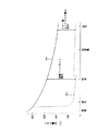
図1は本発明に係る画像形成装置の概略図の一例である。図中1は直径150〜400mmの感光体ドラムで、周速(プロセス速度:vP )500〜2,000mm/秒で回転する。感光体ドラム1の周りには帯電器2、現像機3、転写器4、AC除電器5、イレーズランプ6及びクリーニングブラシ、ブレード、ブロワーの如きクリーニング装置7等が配置されている。図に示すように帯電器2とイレーズランプ6の間にクリーニング装置7が介在されている。
FIG. 1 is an example of a schematic diagram of an image forming apparatus according to the present invention. In the figure,
転写器4の下側に給紙用リトラクタ8が、上側に排紙用リトラクタ9が配置されている。感光体ドラム1の図中右上側には、半導体レーザ、LED、ガスレーザの何れかの露光光源と、ポリゴンミラー、レンズ等からなるスキャナユニット10が配置されている。
A paper feed retractor 8 is disposed below the
As2 Se3 系感光体やアモルファスシリコン系感光体の帯電時間は50m秒〜300m秒、好ましくは50m秒〜200m秒とする。これにより均一で、且つ、帯電後の暗減衰の量を抑止できるとともに実用的な帯電器の寸法とすることが可能である。 The charging time of the As 2 Se 3 photoconductor or the amorphous silicon photoconductor is 50 msec to 300 msec, preferably 50 msec to 200 msec. As a result, the amount of dark decay after charging can be suppressed and the size of a practical charger can be obtained.
帯電器2により一様に帯電された感光体ドラム1にスキャナユニット10から画像光Xが照射され、感光体ドラム1には静電潜像が形成される。その静電潜像は感光体ドラム1の回転に伴い現像機3の方に移動し、現像機3によりトナーが供給されてトナー像として顕像化される。感光体ドラム1上のトナー像は、転写器4により用紙11上に転写される。用紙11は、給紙用リトラクタ8により転写器4及び感光体ドラム1の方へ搬送され、転写の終了した用紙11は排紙用リトラクタ9により図示しない定着装置へ送られ、トナー像は永久像として定着される。
Image light X is irradiated from the
転写の終了した感光体ドラム1は、イレーズランプ6により表面電荷を除電された後、残留トナーをクリーニング装置7により除去され、次の画像形成に備えられる。イレーズランプ6の配置は転写器4とAC除電器5との間でも良く、この方が残像現象の発生を抑止するためには好ましい。イレーズ光の波長λ1 は、As2 Se3 系感光体やアモルファスシリコン系感光体に対してはλ1 ≦780nm、好ましくはλ1 ≦680nmであって、書き込み光の波長λ0 に対してはλ0 −100nm≦λ1 ≦λ0+50nmであるとき、残像現象や光疲労を抑止する上で好ましく、特に600nm≦λ0 ≦680nmのとき有効である。
After the transfer, the
図中の3aは第1現像ロール、3bは第2現像ロール、3cは第3現像ロールで、感光体ドラム1の回転方向上流側から下流側に向けて第1現像ロール3a、第2現像ロール3b、第3現像ロール3cの順に配置されている。12はトナー、13,14,15,16は所定位置に配置された電位センサである。
In the drawing, 3a is a first developing roll, 3b is a second developing roll, 3c is a third developing roll, and the first developing roll 3a and the second developing roll from the upstream side to the downstream side in the rotation direction of the
この画像形成プロセスにおけるAs2 Se3 系感光体ドラム1の表面電位の変化を図2に示す。同図の横軸に帯電、露光、現像、再帯電、転写の画像形成プロセスを示し、縦軸に感光体ドラムの表面電位を示している。図中の実線は非露光部における表面電位、点線は露光部における表面電位をそれぞれ示しており、現像時における非露光部と露光部の表面電位差が現像コントラスト電位、転写直前おける非露光部と露光部の表面電位差がトナー像コントラスト電位である。
FIG. 2 shows changes in the surface potential of the As 2 Se 3
実線の非露光部の電位変化から分かるように、帯電後の感光体表面電位は指数関数的に減少し、帯電から転写までの間の約0.5秒で400V程度の電位低下が生じており、露光直後で700V程度あったコントラスト電位が転写直前では約300V程度になってしまい、暗減衰が大きいため、潜像が崩れる。 As can be seen from the change in the potential of the non-exposed portion of the solid line, the surface potential of the photosensitive member after charging decreases exponentially, and a potential drop of about 400 V occurs in about 0.5 seconds from charging to transfer. The contrast potential, which was about 700 V immediately after exposure, becomes about 300 V immediately before transfer, and dark decay is large, so that the latent image is destroyed.
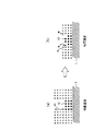
図3は潜像の崩れとトナー像の関係を示す図で、同図(a)は現像直後で潜像の崩れが無い状態、同図(b)は転写直前で潜像が崩れた状態を示している。同図(a)のように潜像の崩れが無い状態では静電潜像に付着したトナー像の乱れを防止する静電的な壁の高さHが高いが、感光体ドラムの暗減衰が大きいため、同図(b)のように前記壁の高さHが急激に低くなると潜像が崩れる。そのため、トナー像を用紙へ転写する際、用紙との擦れ等によりトナーが飛び散りやすくなり、解像度の低下等の画質の低下を生じる。 3A and 3B are diagrams showing the relationship between the collapse of the latent image and the toner image. FIG. 3A shows a state where the latent image is not destroyed immediately after development, and FIG. 3B shows the state where the latent image is destroyed immediately before transfer. Show. In the state where the latent image is not collapsed as shown in FIG. 5A, the height H of the electrostatic wall that prevents the disturbance of the toner image attached to the electrostatic latent image is high, but the dark decay of the photosensitive drum is reduced. Because of its large size, the latent image collapses when the height H of the wall rapidly decreases as shown in FIG. Therefore, when the toner image is transferred to the paper, the toner is likely to be scattered due to rubbing with the paper, and the image quality is deteriorated such as a reduction in resolution.
さらに、潜像書き込み光源や除電光源に、半導体レーザやLED等の赤色光(長波長光)を用いた場合、感光体の電荷保持力はさらに低下する。これは長波長光は感光体中への浸透距離が深く、感光層中に生成される光キャリアの生成位置も深いため、高速印刷のような短いプロセス時間では生成光キャリが感光体中に残留し易いためである。 Furthermore, when red light (long wavelength light) such as a semiconductor laser or LED is used for the latent image writing light source or the neutralization light source, the charge holding power of the photoreceptor is further reduced. This is because long-wavelength light has a deep penetration distance into the photoconductor, and the photocarrier generated in the photoconductive layer is deep, so that the generated light carrier remains in the photoconductor in a short process time such as high-speed printing. It is because it is easy to do.
この解像度低下の防止策の1つとして露光時の初期コントラスト電位を十分に大きくすることが考えられる。しかし、感光膜の体積抵抗が小さく帯電能が小さいAs2 Se3 系感光体を高速で使用し、大きなコントラスト電位を持たせることは、帯電プロセスへの負担が大きくなり、また、感光体自体の耐圧等の問題も生じる(As2 Se3 系感光体の耐圧は約15V/μm程度である)。 As one of the measures for preventing this resolution reduction, it is conceivable to sufficiently increase the initial contrast potential at the time of exposure. However, using an As 2 Se 3 photoconductor with a small volume resistance and a low charging ability at a high speed and having a large contrast potential increases the burden on the charging process. Problems such as breakdown voltage also occur (the breakdown voltage of the As 2 Se 3 photoreceptor is about 15 V / μm).
よって本発明では、耐印刷性に優れ長寿命が期待できるAs2 Se3 系感光体やアモルファスシリコン系感光体を高速で使用しても、カブリや解像度低下を生じることなく、安定して高品質印刷を行うことを目的とし、帯電条件、現像条件、露光・除電条件並びに感光体仕様を適正化した画像形成装置を提供するものである。すなわち、帯電条件では帯電時間の適正化により感光体電位の暗減衰特性とバラツキを改良し、現像条件では現像時間と現像バイアスの適正化により画像濃度とカブリの両立を図った。さらに、感光体の光疲労(残像現象、暗減衰低下)を軽減するため、書き込み光・除電光条件の適正化を図った。 Therefore, in the present invention, even if an As 2 Se 3 photoconductor or an amorphous silicon photoconductor that is excellent in printing resistance and can be expected to have a long life is used at a high speed, it does not cause fogging or a reduction in resolution, and is stably high quality An object of the present invention is to provide an image forming apparatus in which charging conditions, development conditions, exposure / static discharge conditions, and photoconductor specifications are optimized for the purpose of printing. In other words, the dark decay characteristics and variations of the photoreceptor potential were improved by optimizing the charging time under the charging conditions, and both image density and fogging were achieved by optimizing the developing time and developing bias under the developing conditions. Furthermore, in order to reduce photo fatigue (afterimage phenomenon, dark decay reduction) of the photoconductor, the writing light / static discharge light conditions were optimized.
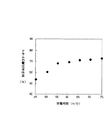
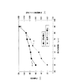
まず、帯電条件について、帯電時間とドラム電位保持率の関係を図4に示す。このテストでは、イレーズ光源に波長600nmのLED(光量:300をμW/cm2 )を用い、感光体はヨウ素を20ppm添加したAs2 Se3 系感光体を使用して、各帯電時間でのドラムの電位保持率を測定した。このドラムの電位保持率は、例えば帯電時間が55m秒のとき、ドラム電位:800V(V0 ) で55m秒間帯電し、その後300m秒間経過後にドラム電位(V1 ) を測定し、V1 /V0 ×100で求めた数値である(この場合、ドラムの電位保持率は70%)。 First, regarding the charging conditions, the relationship between the charging time and the drum potential holding ratio is shown in FIG. In this test, an LED having a wavelength of 600 nm (light quantity: 300 is μW / cm 2 ) is used as an erase light source, and an As 2 Se 3 photoconductor added with 20 ppm of iodine is used as a photoconductor. The potential retention of was measured. For example, when the charging time is 55 msec, the drum potential is charged at a drum potential of 800 V (V 0 ) for 55 msec, and after 300 msec elapse, the drum potential (V 1 ) is measured and V 1 / V This is a numerical value obtained by 0 × 100 (in this case, the drum potential holding ratio is 70%).
同図から明らかのように、帯電時間が50m秒より短い場合には、ドラムの電位保持率が急激に低下している。一方、帯電時間が55m秒より長い場合には、ドラムの電位保持率はほぼ一定である。なお、帯電時間の上限としては装置構成上、約200m秒程度である。この傾向は、帯電器の形状や帯電電流、イレーズ条件、感光体の不純物添加量(1〜500ppm)等の条件において、ほぼ同一であった。このようにAs2 Se3 系感光体は、比較的暗減衰が大きいため、帯電から300m秒経過後のドラムの電位保持率を70%以上とすることで、解像度を保持し、カブリが小さくできる。 As is clear from the figure, when the charging time is shorter than 50 milliseconds, the potential holding ratio of the drum is drastically decreased. On the other hand, when the charging time is longer than 55 milliseconds, the drum potential holding ratio is substantially constant. The upper limit of the charging time is about 200 milliseconds due to the device configuration. This tendency was almost the same in conditions such as the shape of the charger, charging current, erase conditions, and the amount of impurity added to the photoreceptor (1 to 500 ppm). As described above, the As 2 Se 3 photoconductor has a relatively large dark decay. Therefore, by setting the drum potential holding ratio after 70 msec from charging to 70% or more, the resolution can be maintained and the fog can be reduced. .
書き込み光と除電光の波長と、残像現象の関係を図5に示す。このテストでは、書き込み光の光量は感光体(As2 Se3 )の半減露光量の4倍、除電光光量は半減露光量の16倍で行った。残像現象の評価は、1インチベタ黒画像の印刷後、1ライン間隔の横線画像印刷を行い、目視で残像現象の有無を検査した。 FIG. 5 shows the relationship between the wavelength of the writing light and the static elimination light and the afterimage phenomenon. In this test, the amount of writing light was 4 times the half-exposure amount of the photoconductor (As 2 Se 3 ), and the amount of charge removal light was 16 times the half-exposure amount. Evaluation of the afterimage phenomenon was carried out by printing a 1-inch solid black image, printing horizontal line images at intervals of one line, and visually checking for the presence of the afterimage phenomenon.
図中の白丸印は残像現象が発生しなかったもの、黒丸印は残像現象が発生したものを、それぞれ示す。同図から明らかなように、書き込み光の波長:λ0 と除電光波長:λ1 の関係が、λ1 ≧λ0 −100nmであると残像現象の発生が防止できることが分かる。 In the figure, white circles indicate that no afterimage phenomenon has occurred, and black circles indicate that an afterimage phenomenon has occurred. As can be seen from the figure, the afterimage phenomenon can be prevented when the relationship between the wavelength of the writing light: λ 0 and the wavelength of the static elimination light: λ 1 is λ 1 ≧ λ 0 -100 nm.
図6に除電光の波長とドラムの電位保持率の関係を示す。このテストにおけるドラムの電位保持率は、図1中の電位センサ13で測定された露光直後のドラム電位VA と、電位センサ14で測定された現像直後のドラム電位VB との電位の比(VB /VA ×100)で求めた数値である。なお、電位センサ13と電位センサ14の間のプロセス時間は約300m秒である。
FIG. 6 shows the relationship between the wavelength of the static elimination light and the potential holding ratio of the drum. The drum potential holding ratio in this test is the ratio of the drum potential VA immediately after exposure measured by the
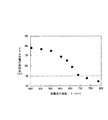
この図から明らかなように、除電光の波長が大きくなるとドラムの電位保持率が低下し、波長が680nmより大きくなるとドラムの電位保持率が50%より低くなり、転写部で十分なコントラスト電位(約300V)を保持することが困難となる。従って除電光の波長は、680nm以下のものを使用する必要がある。 As is clear from this figure, the drum potential holding ratio decreases as the wavelength of the static elimination light increases, and the drum potential holding ratio decreases below 50% when the wavelength exceeds 680 nm. It becomes difficult to maintain about 300V). Accordingly, it is necessary to use a charge elimination light having a wavelength of 680 nm or less.
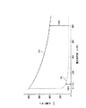
次に感光体条件として、図7に感光体の膜厚と残留電位ならびに限界ドラム表面電位の関係を示す。このテストで、残留電位ならびにドラム電位の測定は図1中の電位センサ14で行った。図中の黒丸印は残留電位を、黒三角印は限界ドラム表面電位を示す。
Next, as the photoreceptor conditions, FIG. 7 shows the relationship between the film thickness of the photoreceptor, the residual potential, and the limit drum surface potential. In this test, the residual potential and the drum potential were measured by the
同図から明らかなように、感光体の膜厚の増大に伴い残留電位と限界ドラム電位が増大する。ここで、残留電位の上昇は画像濃度の低下を招くため、一般に残留電位は100V以下が良好となるため、感光体の膜厚は80μm以下に規制する必要がある。また、限界ドラム表面電位はピンホール等の絶縁破壊を生じず、安定に使用できる表面電位である。よって、十分なコントラスト電位(現像部で約400V以上)を得るためには、感光体の膜厚は40μm以上必要であることが分かる。なお、この関係はアモルファスシリコン系感光体を用いた場合でも同様である。よって感光体の膜厚は40〜80μm、好ましくは50〜75μmの範囲に規制する必要がある。 As is apparent from the figure, the residual potential and the limit drum potential increase as the thickness of the photosensitive member increases. Here, since an increase in the residual potential causes a decrease in image density, the residual potential is generally good at 100 V or less, so that the film thickness of the photoreceptor needs to be regulated to 80 μm or less. The limit drum surface potential is a surface potential that can be stably used without causing dielectric breakdown such as pinholes. Therefore, it can be seen that the film thickness of the photoreceptor needs to be 40 μm or more in order to obtain a sufficient contrast potential (about 400 V or more at the developing portion). This relationship is the same even when an amorphous silicon photoconductor is used. Therefore, it is necessary to regulate the film thickness of the photosensitive member in the range of 40 to 80 μm, preferably 50 to 75 μm.
高速プロセスに用いるAs2 Se3 系感光体は、その光応答特性の改良のため、ヨウ素や塩素などのハロゲン元素の添加が有効である。図8に、ヨウ素の添加量と感光体の電子写真特性(初期電位、残留電位、電位保持率、光応答時間)の関係を示す。 For the As 2 Se 3 photoconductor used in the high-speed process, it is effective to add a halogen element such as iodine or chlorine in order to improve the photoresponse characteristics. FIG. 8 shows the relationship between the amount of iodine added and the electrophotographic characteristics (initial potential, residual potential, potential holding ratio, photoresponse time) of the photoreceptor.
この図から明らかなように、ヨウ素の微量(1ppm以上)の添加により光応答時間は著しく速くなるが、添加量の増大に伴い帯電能や電圧保持率が低下する。ヨウ素の添加量が500ppmを越えると、ドラムの電圧保持率が50%以下となり、十分なコントラスト電位を保持することが困難となる。この傾向は塩素などの他のハロゲン元素においても同様に現れる。よってハロゲン元素の添加量は1〜500ppmの範囲に規制する必要がある。 As is clear from this figure, the addition of a small amount of iodine (1 ppm or more) significantly increases the photoresponse time, but the charging ability and voltage holding ratio decrease as the addition amount increases. When the amount of iodine exceeds 500 ppm, the voltage holding ratio of the drum becomes 50% or less, and it becomes difficult to maintain a sufficient contrast potential. This tendency also appears in other halogen elements such as chlorine. Therefore, it is necessary to regulate the addition amount of the halogen element in the range of 1 to 500 ppm.
図9に、As2 Se3 系感光体の非露光部の暗減衰曲線(A)と露光部の光減衰曲線(B)を示す。測定条件は書き込み光波長:680nm(光量:7mW/cm2 )で、露光出力は感光体ドラム1表面で7mWに設定した。感光体は50ppmのヨウ素を添加したAs2 Se3 系感光体を用いた。
FIG. 9 shows the dark decay curve (A) of the non-exposed portion and the light decay curve (B) of the exposed portion of the As 2 Se 3 photoconductor. Measurement conditions were a writing light wavelength: 680 nm (light quantity: 7 mW / cm 2 ), and an exposure output was set to 7 mW on the surface of the
同図の光減衰曲線(B)から、残留電位がほぼ安定する(残留電位が約100V以下となる)のに露光後70m秒以上の時間が必要であることが分かる。また、露光後の時間が800m秒を越えると、表面電位の暗減衰により非露光部のドラム電位が400V以下となり、十分なコントラスト電位が得られないため、カブリ等の画像不良を生じやすくなる。従って、露光から現像開始までのプロセス時間T1 は、70m秒以上必要である。 From the light attenuation curve (B) in the figure, it can be seen that a time of 70 milliseconds or more after exposure is required for the residual potential to become almost stable (the residual potential is about 100 V or less). On the other hand, if the time after exposure exceeds 800 milliseconds, the drum potential of the non-exposed part becomes 400 V or less due to dark decay of the surface potential, and a sufficient contrast potential cannot be obtained. Therefore, the process time T 1 from exposure to the start of development needs to be 70 ms or more.
図10に露光から現像開始までの時間と限界解像度の関係を示す。このテストは、As2 Se3 系感光体を用い、書き込み光源には波長680nmの半導体レーザを使用し、イレーズ光源には600nmのLED(光量:300μW/cm2 )を用いた。現像条件は3本の現像ロールを備えた現像機で、現像剤は2成分現像剤を用い、トナーには平均粒径が11μmのスチレンアクリル系トナーとした。また、感光体表面電位は現像機直前部で約800V、現像コントラスト電位:300Vの条件である。感光体にはヨウ素を20ppm、500ppm添加したAs2 Se3 系感光体と無添加As2 Se3 系感光体を用い、感光体の表面粗さは0.75μmとした。 FIG. 10 shows the relationship between the time from exposure to the start of development and the limit resolution. In this test, an As 2 Se 3 photoconductor was used, a semiconductor laser having a wavelength of 680 nm was used as a writing light source, and an LED (light amount: 300 μW / cm 2 ) was used as an erase light source. The developing conditions were a developing machine equipped with three developing rolls, a two-component developer was used as the developer, and a styrene acrylic toner having an average particle diameter of 11 μm was used as the toner. The photosensitive member surface potential is about 800 V immediately before the developing machine and a development contrast potential of 300 V. As the photoconductor, an As 2 Se 3 photoconductor added with 20 ppm and 500 ppm of iodine and an additive-free As 2 Se 3 photoconductor were used, and the surface roughness of the photoconductor was 0.75 μm.
また解像度の評価は、MF(Modulation Function)の測定によるドット再現性の評価にて行なった。ここでMFとは画像のコントラストを変調度で評価するものであり、1ドットオン1ドットオフ画像の画像濃度をマイクロデンシトメータで測定し、その平均濃度を基準として高濃度値と低濃度値の平値Dmax とDmin を求め、以下の式により算出した。 The resolution was evaluated by evaluating dot reproducibility by measuring MF (Modulation Function). Here, MF evaluates the contrast of an image by the degree of modulation. The image density of a 1 dot on 1 dot off image is measured with a microdensitometer, and a high density value and a low density value are based on the average density. The average values Dmax and Dmin were calculated and calculated by the following formula.
FM値=(Dmax −Dmin )/(Dmax +Dmin )×100(%)
従ってMF値が大きいほどドット再現性が良いことになり、今回はMF値50%以上を合格値とした。また解像度の目標値は600dpiである。
FM value = (D max −D min ) / (D max + D min ) × 100 (%)
Accordingly, the larger the MF value, the better the dot reproducibility, and this time, an MF value of 50% or more was set as a pass value. The target value of resolution is 600 dpi.
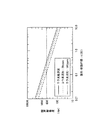
この図10から露光−現像時間が長くなるほど、得られる限界解像度は小さくなることが分かる。これは感光体上に形成されたドットの潜像が時間の経過に伴って崩れ、再現性が低下するためである。また、感光体へのハロゲン元素(ここではヨウ素)の添加量が増加するほど、同一露光−現像時間における限界解像度が低下することが分かる。これはハロゲン元素の添加により感光体の材料抵抗が低下し、潜像が崩れ易くなったためである。この図10の結果から、目標である解像度600dpiを達成するためには、露光−現像時間を300m秒以内に設定する必要があることが分かる。 From FIG. 10, it can be seen that the longer the exposure-development time, the smaller the limit resolution obtained. This is because the latent image of the dots formed on the photoconductor collapses over time and the reproducibility decreases. It can also be seen that the limit resolution in the same exposure-development time decreases as the amount of halogen element (iodine here) added to the photoreceptor increases. This is because the material resistance of the photoreceptor is lowered by the addition of the halogen element, and the latent image is easily broken. From the results shown in FIG. 10, it can be seen that the exposure-development time must be set within 300 milliseconds in order to achieve the target resolution of 600 dpi.
図11に、現像時間(現像ロールが複数本の場合はそれらの合計)と、画像濃度、カブリ濃度の関係を示す。図中の黒丸印は現像時間と画像濃度の関係を示し、黒三角印は現像時間とカブリ濃度の関係を示す。画像濃度の評価はベタ黒印刷サンプルの画像の反射濃度測定(測定機:Graphtcs Microsystems Inc,社製商品名マクベス反射濃度計)で、カブリ濃度の評価は白紙印刷サンプルと未印刷紙の印刷濃度非評価(測定機:Hunter Associates Laboratory Inc,社製商品名ハンター濃度計)で、それぞれ行った。 FIG. 11 shows the relationship between the development time (when there are a plurality of development rolls, the total thereof), the image density, and the fog density. In the figure, black circles indicate the relationship between development time and image density, and black triangles indicate the relationship between development time and fog density. The image density is evaluated by measuring the reflection density of an image of a solid black print sample (measuring device: Graphcs Microsystems Inc., product name: Macbeth reflection densitometer). The evaluation was performed (measuring instrument: Hunter Associates Laboratory Inc., trade name Hunter densitometer).
同図に示すように、現像時間が50m秒以上で、画像濃度が約1.4(D)以上となるが、現像時間が長くなるに従いカブリ濃度も増加し、現像時間が200m秒を越えると、カブリ濃度が約0.8%以上となる。従って、現像時間は50〜200m秒、好ましくは60〜100m秒の範囲に規制する必要がある。 As shown in the figure, when the development time is 50 ms or more and the image density is about 1.4 (D) or more, the fog density increases as the development time becomes longer, and when the development time exceeds 200 ms. The fog density is about 0.8% or more. Therefore, it is necessary to regulate the development time in the range of 50 to 200 milliseconds, preferably 60 to 100 milliseconds.
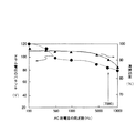
現像バイアス条件と画像濃度、カブリ濃度の関係を図12に示す。このテストは、図1に示すように3本の現像ロール3a〜3cを備えた現像機で、現像剤は2成分現像剤を用い、トナーには平均粒径11μmのスチレンアクリル系トナーを使用した。また、感光体の表面電位は現像機直前で約750Vである。 FIG. 12 shows the relationship between the developing bias condition, the image density, and the fog density. In this test, as shown in FIG. 1, a developing machine having three developing rolls 3a to 3c, a two-component developer was used as a developer, and a styrene acrylic toner having an average particle diameter of 11 μm was used as a toner. . The surface potential of the photoreceptor is about 750 V just before the developing machine.
同図に示すように3本の現像ロール(第1ロール、第2ロール、第3ロール)に印加する現像バイアス電圧を種々変えた場合の画像濃度とカブリ濃度を調べた結果、現像バイアス電圧を感光体回転方向の下流側に向かって小さくすることで、カブリが低減できることが分かった。 As shown in the figure, as a result of examining the image density and the fog density when the development bias voltages applied to the three development rolls (first roll, second roll, and third roll) are variously changed, the development bias voltage is determined as follows. It has been found that the fog can be reduced by decreasing the size toward the downstream side in the rotation direction of the photosensitive member.
図13に、転写部のコントラスト電位と1ドットラインの線幅の関係を示す。この測定は図1に示す装置で行い、コントラスト電位の測定は図1中の電位センサ15で行った。また、書き込み光のドラム面上でのスポット径は約100μmであり、240dpi相当の光学系を使用した。
FIG. 13 shows the relationship between the contrast potential of the transfer portion and the line width of one dot line. This measurement was performed with the apparatus shown in FIG. 1, and the contrast potential was measured with the
同図から明らかなように、転写部のコントラスト電位の低下に従い線幅が太くなり、解像度が低下しているのが分かる。現像条件等により若干の線太りが生じるため、限界の線幅を120μmと設定すると、転写部のコントラスト電位が300V以上で、1ドットラインの線幅が120μm以下となることが分かる。 As can be seen from the figure, the line width increases as the contrast potential of the transfer portion decreases, and the resolution decreases. Since a slight line thickening occurs depending on development conditions and the like, it can be seen that when the limit line width is set to 120 μm, the contrast potential of the transfer portion is 300 V or more and the line width of one dot line is 120 μm or less.
図14に、AC除電器の周波数とドラム電位のばらつき、ならびに清掃効率の関係を示す。このテストで、AC除電器の印加電圧は実行値で約5kVとし、電位のばらつきの測定は図1中の電位センサ16で行った。図中の黒丸印はAC除電器の周波数とドラム電位のばらつきの関係を、黒三角印はAC除電器の周波数と清掃効率の関係を、それぞれ示す。
FIG. 14 shows the relationship between the frequency of the AC static eliminator, the variation in drum potential, and the cleaning efficiency. In this test, the applied voltage of the AC static eliminator was about 5 kV as an execution value, and the variation in potential was measured by the
同図から明らかなように、AC除電器の周波数が500Hzより小さい場合、ドラム電位のばらつきが急激に増大し、100V以上の電位のばらつきとなる。また、周波数が増大するに従い清掃効率は徐々に低下し、周波数が7,000Hzを越えると、清掃効率が85%以下となってしまうことが分かる。この傾向は、印加電圧が2kV〜7kVの範囲でほぼ同等であった。これらの事から、AC除電器の周波数は500〜7,000Hzの範囲、好ましくは500〜2,000Hzの範囲が望ましい。 As is clear from the figure, when the frequency of the AC static eliminator is smaller than 500 Hz, the variation in drum potential increases rapidly, resulting in a variation in potential of 100 V or more. Further, it can be seen that the cleaning efficiency gradually decreases as the frequency increases, and that the cleaning efficiency becomes 85% or less when the frequency exceeds 7,000 Hz. This tendency was almost the same when the applied voltage was in the range of 2 kV to 7 kV. For these reasons, the frequency of the AC static eliminator is in the range of 500 to 7,000 Hz, preferably in the range of 500 to 2,000 Hz.
次に本発明の具体例について説明する。
(実施例1)
図1に示す画像形成装置において、スキャナユニット10の書き込み露光光源にはInGaAlP/GaAs系の半導体レーザ(波長680nm)を使用し、露光出力は感光体ドラム1表面で約6mWに設定した。感光体ドラム1は、光応答性向上のためヨウ素を20ppm添加したAs2 Se3 系感光体(形状:外径262mm×長さ430mm、膜厚:60μm)を用いた。感光体ドラム1の回転数は60rpmで、露光部と現像機3間のプロセス時間は約180m秒である。
Next, specific examples of the present invention will be described.
Example 1
In the image forming apparatus shown in FIG. 1, an InGaAlP / GaAs semiconductor laser (wavelength 680 nm) was used as a writing exposure light source of the
本発明による画像形成は、次のようにして行った。まず、帯電器2に約+7.5kVの電圧印加により感光体ドラム1に約+800Vの表面電位を帯電させる。帯電器2のコロナワイヤの直径は70μm、各ワイヤ間距離ならびにドラムとワイヤ間距離は約10mmとし、帯電器2のドラム周方向の幅を80mmとした。
Image formation according to the present invention was performed as follows. First, a surface potential of about +800 V is charged to the
次にスキャナユニット10により像露光を行い、感光体ドラム1の表面に潜像を形成する。ここで、本実施例では、レーザ露光スポット径は約70μm、解像度480dpiの仕様とした。現像機3は3本の現像ロール3a〜3cを備えた多段式現像機を使用し、各現像ロールの径は50mmで、現像時間は約90m秒とした。現像剤は2成分現像剤を用い、トナー12は平均粒径が11μmのスチレンアクリル系トナーとした。現像バイアス電圧は感光体ドラム1の回転方向の上流側から下流側に向けて400V/350V/300Vと設定した。
Next, image exposure is performed by the
現像機3により顕像化されたトナー像は、転写器4で用紙11に転写される。転写電圧は約−6.0kVとした。未転写の残留トナーはその後のAC除電器5(AC周波数:500Hz、印加電圧:5kV)で除電され、また、感光体ドラム1上の静電潜像はイレーズランプ6(15W白色蛍光灯に赤色フィルタを介し、波長約660nm、光量:300μW/cm2 の赤色光)で除電される。その後、クリーニング装置7(本実施例では、クリーニングにはファーブラシを用いた)により感光体ドラム1の表面はクリーニングされ、次の画像形成に備えられる。
The toner image visualized by the developing device 3 is transferred to the
13,14,15は表面電位センサである。センサ13は露光直後、センサ14は現像機直後、センサ15は転写直前に設置され、感光体ドラム1の表面電位値の検出を行った。上記画像形成条件によるドラム電位は、センサ13の位置で非露光部電位:V0 /露光部電位:VR =800V/90V、センサ14の位置で630V/105V、センサ15の位置で500V/100Vであった。帯電後300m秒での電圧保持率は70%、残留電位は85Vであった。
以上の条件で、約5,000頁の印刷試験を行った結果、印刷サンプルは、ベタ濃度が1.45(D)、カブリ濃度が0.4%、解像度は480dpi相当の高精細の画質が得られた。また、長期間にわたりこれを維持でき、300万頁の印刷においても、実用的な画像が得られた。 As a result of performing a print test of about 5,000 pages under the above conditions, the print sample has a solid image density of 1.45 (D), a fog density of 0.4%, and a high definition image quality equivalent to 480 dpi. Obtained. Moreover, this could be maintained over a long period of time, and a practical image was obtained even when printing 3 million pages.
(実施例2)
書き込み露光光源には赤色LED(波長680nm)を使用し、露光出力は感光体ドラム1表面で約6mWに設定した。感光体ドラム1は、光応答性向上のためヨウ素を300ppm添加したAs2 Se3 系感光体(形状:外径262mm×長さ430mm)を用い、感光体の膜厚は40μmとした。感光体ドラム1の回転数は60rpmで、露光部と現像機3間のプロセス時間は約150m秒である。帯電器2の幅は110mmとし、感光体の帯電時間を約133m秒と設定した。LED露光スポット径は約40μm、解像度600dpiの仕様とした。
(Example 2)
A red LED (wavelength 680 nm) was used as the writing exposure light source, and the exposure output was set to about 6 mW on the surface of the
現像機3は、実施例1と同一とし、現像時間は約95m秒とした。現像剤は2成分現像剤を用い、トナー12は平均粒径が7μmのスチレンアクリル系トナーとした。現像バイアス電圧は感光体ドラム1の回転方向の上流側から400V/350V/300Vと設定した。イレーズランプ6は波長660nmLED(光量:400μW/cm2 )を採用した。
The developing machine 3 was the same as in Example 1, and the development time was about 95 milliseconds. As the developer, a two-component developer was used, and the
他の画像形成条件は実施例1と同一として約5,000頁の印刷試験を行ったところ、ドラム電位は、電位センサ13の位置で非露光部電位:V0 /露光部電位:VR =800V/80V、電位センサ14の位置で630V/100V、電位センサ15の位置で510V/100Vであった。帯電後300m秒での電圧保持率は70%、残留電位は75Vであった。また印刷サンプルは、ベタ濃度が1.45(D)、カブリ濃度が0.45%、解像度は600dpi相当の高精細の画質が得られた。また、長期間にわたりこれを維持でき、300万頁の印刷においても、実用的な画像が得られた。
The other image forming conditions were the same as in Example 1, and a printing test of about 5,000 pages was performed. As a result, the drum potential at the position of the
(実施例3)
書き込み露光光源にHeNeレーザ(波長635nm)を使用し、露光出力は感光体ドラム1表面で約6mWに設定した。感光体ドラム1は、光応答性向上のためヨウ素を10ppm添加したAs2 Se3 系感光体(形状:外径262mm×長さ430mm、膜厚:60μm)を用いた。感光体ドラム1の回転数は72rpmで、露光部と現像機3間のプロセス時間は約125m秒である。
(Example 3)
A HeNe laser (wavelength 635 nm) was used as the writing exposure light source, and the exposure output was set to about 6 mW on the surface of the
本実施例による画像形成は以下のようにして行った。まず、帯電器2に約+8.5kVの電圧印加により感光体ドラム1に約+800Vの表面電位を帯電させる。帯電器2のコロナワイヤの直径は70μm、各ワイヤ間距離ならびにドラムとワイヤ間距離は約10mmとし、帯電器2のドラム周方向の幅を110mmとすることで、感光体の帯電時間を約111m秒と設定した。
Image formation according to this example was performed as follows. First, a surface potential of about +800 V is charged to the
次にスキャナユニット10により像露光を行い、感光体ドラム1の表面に潜像を形成する。ここで、本実施例では、レーザ露光スポット径は約70μm、解像度480dpiの仕様とした。
Next, image exposure is performed by the
現像機3は、現像ロールを3本備えた多段式現像機を使用し、各現像ロール径は50mmで、現像時間は約80m秒とした。現像剤は2成分現像剤を用い、トナー12は平均粒径が11μmのスチレンアクリル系トナーとした。現像バイアス電圧は感光体ドラム1の回転方向の上流側から下流側に向けて350V/300V/250Vと設定した。
As the developing machine 3, a multi-stage developing machine provided with three developing rolls was used, each developing roll diameter was 50 mm, and the developing time was about 80 milliseconds. As the developer, a two-component developer was used, and the
現像機3により顕像化されたトナー像は、転写器4で用紙11に転写される。転写電圧は約−6.0kVとした。未転写の残留トナーはその後のAC除電器5(AC周波数:5kHz、印加電圧:5kV)で除電され、また、感光体上の静電潜像はイレーズランプ6(15W白色蛍光灯に赤色フィルタを介し、波長約600nm、光量:250μW/cm2 の赤色光)で除電される。
The toner image visualized by the developing device 3 is transferred to the
上記画像形成条件によるドラム電位は、電位センサ13の位置で非露光部電位:V0 /露光部電位:VR =800V/85V、電位センサ14の位置で680V/105V、電位センサ15の位置で550V/100Vであり、約5,000頁の印刷試験を行った結果、印刷サンプルは、ベタ濃度が1.35(D)、カブリ濃度が0.4%、解像度は480dpi相当の高精細の画質が得られた。また、長期間にわたりこれを維持でき、300万頁の印刷においても、実用的な画像が得られた。
The drum potential according to the image forming conditions is as follows: non-exposed portion potential: V0 / exposed portion potential: VR = 800V / 85V at the position of the
(実施例4)
書き込み露光光源にArレーザ(波長488nm)を使用し、露光出力は感光体ドラム1表面で約8mWに設定した。感光体ドラム1は、光応答性向上のためヨウ素を3ppm添加したAs2 Se3 系感光体(形状:外径262mm×長さ430mm)を用い、感光体の膜厚は50μmとした。感光体ドラム1の回転数は80rpmで、露光部と現像機3間のプロセス時間は約120m秒である。帯電器2の幅は110mmとし、感光体の帯電時間を約100m秒と設定した。LED露光スポット径は約40μm、解像度600dpiの仕様とした。
Example 4
An Ar laser (wavelength 488 nm) was used as a writing exposure light source, and the exposure output was set to about 8 mW on the surface of the
現像機3は、現像ロールを4本備えた多段式現像機を使用し、現像ロール径は50mmで、現像時間は約90m秒とした。現像剤は2成分現像剤を用い、トナー12は平均粒径が7μmのスチレンアクリル系トナーとした。現像バイアス電圧は感光体ドラムの回転方向の上流側から下流側に向けて400V/350V/300V/250Vと設定した。イレーズランプ6は15W白色蛍光灯に青色フィルタ(BPB45)を介し、波長約450nm、光量:250μW/cm2 とした。
As the developing machine 3, a multistage developing machine having four developing rolls was used, the developing roll diameter was 50 mm, and the developing time was about 90 milliseconds. As the developer, a two-component developer was used, and the
他の画像形成条件は実施例3と同一として約5,000頁の印刷試験を行ったところ、ドラム電位は、電位センサ13の位置で非露光部電位:V0 /露光部電位:VR =800V/75V、電位センサ14の位置で700V/85V、電位センサ15の位置で610V/85Vであり、印刷サンプルは、ベタ濃度が1.50(D)、カブリ濃度が0.3%、解像度は600dpi相当の高精細の画質が得られた。また、長期間にわたりこれを維持でき、300万頁の印刷においても、実用的な画像が得られた。
When the other image forming conditions were the same as in Example 3 and a printing test of about 5,000 pages was performed, the drum potential at the position of the
(実施例5)
書き込み露光光源に半導体レーザ(波長635nm)を4個をアレイ状で使用し、露光出力は感光体ドラム1表面で約8mWに設定した。感光体ドラム1は、光応答性向上のため塩素を50ppm添加したAs2 Se3 系感光体(形状:外径262mm×長さ430mm)を用い、感光体の膜厚は45μmとした。感光体ドラム1の回転数は80rpmで、露光部と現像機3間のプロセス時間は約120m秒である。帯電器2の幅は80mmとし、感光体の帯電時間を約73m秒と設定した。LED露光スポット径は約40μm、解像度600dpiの仕様とした。
(Example 5)
Four semiconductor lasers (wavelength 635 nm) were used in an array form as a writing exposure light source, and the exposure output was set to about 8 mW on the surface of the
現像機3は、現像ロールを4本備えた多段式現像機を使用し、現像ロール径は50mmで、現像時間は約90m秒とした。現像剤は2成分現像剤を用い、トナー12は平均粒径が7μmのスチレンアクリル系トナーとした。現像バイアス電圧は感光体ドラムの回転方向の上流側から400V/350V/300V/250Vと設定した。イレーズランプ6は波長600nmのLEDアレイ(光量:350μW/cm2 )使用した。
As the developing machine 3, a multistage developing machine having four developing rolls was used, the developing roll diameter was 50 mm, and the developing time was about 90 milliseconds. As the developer, a two-component developer was used, and the
他の画像形成条件は実施例4と同一として約5,000頁の印刷試験を行ったところ、ドラム電位は、(A)位置で非露光部電位:V0 /露光部電位:VR =800V/85V、(B)位置で660V/100V、(C)位置で500V/100Vであり、印刷サンプルは、ベタ濃度が1.45(D)、カブリ濃度が0.5%、解像度は600dpi相当の高精細の画質が得られた。また、長期間にわたりこれを維持でき、300万頁の印刷においても実用的な画像が得られた。 When the other image forming conditions were the same as in Example 4 and a printing test of about 5,000 pages was performed, the drum potential was the non-exposed portion potential: V0 / exposed portion potential: VR = 800 V / 85 V at the position (A). , (B) position is 660V / 100V, (C) position is 500V / 100V, the print sample has a solid density of 1.45 (D), fog density of 0.5%, resolution is high definition equivalent to 600 dpi The image quality of was obtained. In addition, this could be maintained over a long period of time, and a practical image was obtained even when printing 3 million pages.
(実施例6)
図1に示す装置において、スキャナユニット10における書き込み露光光源にnGaAlP/GaAs系の半導体レーザ(波長680nm)を使用し、露光出力は感光体ドラム1表面で約6mWに設定した。感光体ドラム1は、光応答性向上のためヨウ素を20ppm添加したAs2 Se3 系感光体(形状:外径262mm×長さ430mm、膜厚:60μm)を用い、表面粗さは0.375μmとした。感光体ドラム1の回転数は60rpmで、露光部と現像機3間のプロセス時間は約180m秒である。
(Example 6)
In the apparatus shown in FIG. 1, an nGaAlP / GaAs semiconductor laser (wavelength 680 nm) was used as a writing exposure light source in the
本発明による画像形成は、以下のようにして行った。まず、帯電器2に約+7.5kVの電圧印加により感光体ドラム1に約+800Vの表面電位を帯電させる。帯電器2のコロナワイヤの直径は70μm、各ワイヤ間距離ならびにドラムとワイヤ間距離は約10mmとした。また、帯電器2のドラム周方向の幅を80mmとした。
Image formation according to the present invention was performed as follows. First, a surface potential of about +800 V is charged to the
次に、スキャナユニット10により像露光を行い、感光体ドラム1の表面に潜像を形成する。本実施例では、レーザ露光スポット径は約45μm、解像度600dpiの仕様とした。現像機3は、現像ロールを3本備えた多段式現像機を使用し、現像ロール径は50mmで、現像時間は約90m秒とした。現像剤は2成分現像剤を用い、トナー12は平均粒径が11μmのスチレンアクリル系トナーとした。現像バイアス電圧は感光体ドラムの回転方向の上流側から下流側に向けて400V/350V/300Vと設定した。
Next, image exposure is performed by the
現像機3により顕像化されたトナー像は、転写器4で用紙11に転写される。転写電圧は約−6.0kVとした。未転写の残留トナーはその後のAC除電器5(AC周波数:500Hz、印加電圧:5kV)で除電され、また、感光体上の静電潜像はイレーズランプ6(15W白色蛍光灯に赤色フィルタを介し、波長約660nm、光量:300μW/cm2 の赤色光)で除電される。その後、クリーニング装置7(本実施例では、クリーニングにはファーブラシを用いた)により感光体ドラム1の表面はクリーニングされ、次の画像形成に備えられる。
The toner image visualized by the developing device 3 is transferred to the
上記画像形成条件によるドラム電位は、電位センサ13の位置で非露光部電位:V0 /露光部電位:VR =800V/90V、電位センサ14の位置で630V/105V、電位センサ15の位置で500V/100Vであった。帯電後300m秒での電圧保持率は70%、残留電位は85Vであった。
The drum potential according to the image forming conditions is as follows: non-exposed portion potential: V0 / exposed portion potential: VR = 800 V / 90 V at the position of the
以上の条件で、約5,000頁の印刷試験を行った結果、印刷サンプルは、ベタ濃度が1.45(D)、カブリ濃度が0.4%(カブリ濃度;Nはハンター色差濃度計で測定し次の式で求めた。N=γmax −γA 、γmax ;紙の反射率( 最大反射率) 、γA ;測定領域A 中の平均反射率)、MF値は68%、解像度は600dpi相当の高精細の画質が得られた。また、長期間にわたりこれを維持でき、300万頁の印刷においても、実用的な画像が得られた。 As a result of performing a printing test of about 5,000 pages under the above conditions, the printed sample has a solid density of 1.45 (D) and a fog density of 0.4% (fog density; N is a Hunter color difference densitometer. Measured and obtained by the following formula: N = γmax−γA, γmax: paper reflectance (maximum reflectance), γA: average reflectance in the measurement area A), MF value is 68%, resolution is equivalent to 600 dpi High definition image quality was obtained. Moreover, this could be maintained over a long period of time, and a practical image was obtained even when printing 3 million pages.
(実施例7)
書き込み露光光源には赤色LED(波長780nm)を使用し、露光出力は感光体ドラム1表面で約6mWに設定した。感光体ドラム1は、光応答性向上のためヨウ素を300ppm添加したAs2 Se3 系感光体(形状:外径262mm×長さ430mm)を用い、感光体の膜厚は40μm、表面粗さは0.75μmとした。感光体ドラム1の回転数は60rpmで、露光部と現像機3間のプロセス時間は約70m秒である。帯電器2の幅は110mmとし、感光体の帯電時間を約133m秒と設定した。LED露光スポット径は約40μm、解像度600dpiの仕様とした。
(Example 7)
A red LED (
現像機3は、実施例6と同一とし、現像時間は約95m秒とした。現像剤は2成分現像剤を用い、トナー12は平均粒径が7μmのスチレンアクリル系トナーとした。現像バイアス電圧は感光体ドラムの回転方向の上流側から下流側に向けて400V/350V/300Vと設定した。イレーズランプ6は波長660nmLED(光量:400μW/cm2 )を採用した。
The developing machine 3 was the same as in Example 6, and the development time was about 95 milliseconds. As the developer, a two-component developer was used, and the
他の画像形成条件は実施例6と同一として約5,000頁の印刷試験を行ったところ、ドラム電位は、電位センサ13の位置で非露光部電位:V0 /露光部電位:VR =800V/80V、電位センサ14の位置で630V/100V、電位センサ15の位置で510V/100Vであった。帯電後300m秒での電圧保持率は70%、残留電位は75Vであった。また印刷サンプルは、ベタ濃度が1.45(D)、カブリ濃度が0.45%、MF値が60%、解像度は600dpi相当の高精細の画質が得られた。また、長期間にわたりこれを維持でき、300万頁の印刷においても、実用的な画像が得られた。
The other image forming conditions were the same as in Example 6, and a printing test of about 5,000 pages was performed. The drum potential at the position of the
(実施例8)
書き込み露光光源にHeNeレーザ(波長635nm)を使用し、露光出力は感光体ドラム1表面で約6mWに設定した。感光体ドラム1は、光応答性向上のためヨウ素を10ppm添加したAs2 Se3 系感光体(形状:外径262mm×長さ430mm、膜厚:60μm)を用いた。また、表面粗さは1.5μmとした。感光体ドラム1の回転数は72rpmで、露光部と現像機3間のプロセス時間は約125m秒である。
(Example 8)
A HeNe laser (wavelength 635 nm) was used as the writing exposure light source, and the exposure output was set to about 6 mW on the surface of the
本実施例による画像形成は以下のようにして行った。まず、帯電器2に約+8.5kVの電圧印加により感光体ドラム1に約+800Vの表面電位を帯電させる。帯電器2のコロナワイヤの直径は70μm、各ワイヤ間距離ならびにドラムとワイヤ間距離は約10mmとした。また、帯電器2のドラム周方向の幅を110mmとすることで、感光体の帯電時間を約111m秒と設定した。次に、スキャナユニット10により像露光を行い、感光体ドラム1の表面に潜像を形成する。ここで、本実施例では、レーザ露光スポット径は約35μm、解像度800dpiの仕様とした。
Image formation according to this example was performed as follows. First, a surface potential of about +800 V is charged to the
現像機3は、現像ロールを3本備えた多段式現像機を使用し、現像ロール径は50mmで、現像時間は約80m秒とした。現像剤は2成分現像剤を用い、トナー12は平均粒径が11μmのスチレンアクリル系トナーとした。現像バイアス電圧は感光体ドラムの回転方向の上流側から下流側に向けて350V/300V/250Vと設定した。
As the developing machine 3, a multistage developing machine having three developing rolls was used, the developing roll diameter was 50 mm, and the developing time was about 80 milliseconds. As the developer, a two-component developer was used, and the
現像機3により顕像化されたトナー像は、転写器4で用紙11に転写される。転写電圧は約−6.0kVとした。未転写の残留トナーはその後のAC除電器5(AC周波数:5kHz、印加電圧:5kV)で除電され、また、感光体上の静電潜像はイレーズランプ6(15W白色蛍光灯に赤色フィルタを介し、波長約600nm、光量:250μW/cm2 の赤色光)で除電される。
The toner image visualized by the developing device 3 is transferred to the
上記画像形成条件によるドラム電位は、電位センサ13の位置で非露光部電位:V0 /露光部電位:VR =800V/85V、電位センサ14の位置で680V/105V、電位センサ15の位置で550V/100Vであり、約5,000頁の印刷試験を行った結果、印刷サンプルは、ベタ濃度が1.35(D)、カブリ濃度が0.4%、MF値が55%以上の高精細の画質が得られた。また、長期間にわたりこれを維持でき、300万頁の印刷においても、実用的な画像が得られた。
The drum potential according to the image forming conditions is as follows: non-exposed portion potential: V0 / exposed portion potential: VR = 800V / 85V at the position of the
(実施例9)
書き込み露光光源にArレーザ(波長488nm)を使用し、露光出力は感光体ドラム1表面で約8mWに設定した。感光体ドラム1は、光応答性向上のためヨウ素を3ppm添加したAs2 Se3 系感光体(形状:外径262mm×長さ430mm、表面粗さ:0.75μm)を用い、感光体の膜厚は50μmとした。感光体ドラム1の回転数は80rpmで、露光部と現像機3間のプロセス時間は約80m秒である。帯電器2の幅は110mmとした。Ar(アルゴン)露光スポット径は約40μm、解像度600dpiの仕様とした。
Example 9
An Ar laser (wavelength 488 nm) was used as a writing exposure light source, and the exposure output was set to about 8 mW on the surface of the
現像機3は、現像ロールを4本備えた多段式現像機を使用し、現像ロール径は50mmで、現像時間は約90m秒とした。現像剤は2成分現像剤を用い、トナー12は平均粒径が7μmのスチレンアクリル系トナーとした。現像バイアス電圧は感光体ドラムの回転方向の上流側から下流側に向けて400V/350V/300V/250Vと設定した。イレーズランプ6は15W白色蛍光灯に青色フィルタ(BPB45)を介し、波長約450nm、光量:250μW/cm2 とした。
As the developing machine 3, a multistage developing machine having four developing rolls was used, the developing roll diameter was 50 mm, and the developing time was about 90 milliseconds. As the developer, a two-component developer was used, and the
他の画像形成条件は実施例8と同一として約5,000頁の印刷試験を行ったところ、ドラム電位は、電位センサ13の位置で非露光部電位:V0 /露光部電位:VR =800V/75V、電位センサ14の位置で700V/85V、電位センサ15の位置で610V/85Vであり、印刷サンプルは、ベタ濃度が1.50(D)、カブリ濃度が0.3%、MF値が70%の高精細の画質が得られた。また、長期間にわたりこれを維持でき、300万頁の印刷においても、実用的な画像が得られた。
The other image forming conditions were the same as in Example 8, and a printing test of about 5,000 pages was performed. As a result, the drum potential at the position of the
(実施例10)
書き込み露光光源に半導体レーザ(波長635nm)を4個をアレイ状で使用し、露光出力は感光体ドラム1表面で約8mWに設定した。感光体ドラム1は、光応答性向上のため塩素を50ppm添加したAs2 Se3 系感光体(形状:外径262mm×長さ430mm)を用い、感光体の膜厚は45μm、表面粗さは0.375μmとした。感光体ドラム1の回転数は80rpmで、露光部と現像機3間のプロセス時間は約200m秒である。帯電器2の幅は80mmとし、感光体の帯電時間を約73m秒と設定した。半導体レーザ露光スポット径は約40μm、解像度600dpiの仕様とした。
(Example 10)
Four semiconductor lasers (wavelength 635 nm) were used in an array form as a writing exposure light source, and the exposure output was set to about 8 mW on the surface of the
現像機3は、現像ロールを4本備えた多段式現像機を使用し、現像ロール径は50mmで、現像時間は約90m秒とした。現像剤は2成分現像剤を用い、トナー12は平均粒径が7μmのスチレンアクリル系トナーとした。現像バイアス電圧は感光体ドラムの回転方向の上流側から下流側に向けて400V/350V/300V/250Vと設定した。イレーズランプ6は波長600nmのLEDアレイ(光量:350μW/cm2 )使用した。
As the developing machine 3, a multistage developing machine having four developing rolls was used, the developing roll diameter was 50 mm, and the developing time was about 90 milliseconds. As the developer, a two-component developer was used, and the
他の画像形成条件は実施例9と同一として約5,000頁の印刷試験を行ったところ、ドラム電位は、電位センサ13の位置で非露光部電位:V0 /露光部電位:VR =800V/85V、電位センサ14の位置で660V/100V、電位センサ15の位置で500V/100Vであり、印刷サンプルは、ベタ濃度が1.45(D)、カブリ濃度が0.5%、MF値が65%の高精細の画質が得られた。また、長期間にわたりこれを維持でき、300万頁の印刷においても実用的な画像が得られた。
The other image forming conditions were the same as in Example 9, and a printing test of about 5,000 pages was performed. The drum potential at the position of the
1 感光体ドラム
2 帯電器
3 現像機
4 転写器
5 AC除電器
6 イレーズランプ
7 クリーニング装置
10 スキャナユニット
11 用紙
12 トナー
13〜16 電位センサ
DESCRIPTION OF
Claims (5)
前記感光体が三セレン化砒素またはアモルファスシリコンを母材とする感光体であって、
前記露光に使用する書き込み光の波長λ0 と、現像後の感光体を除電する除電光の波長λ1 が下記の関係にあることを特徴とする画像形成装置。
λ0 −100nm≦λ1 ≦680nm In an image forming apparatus that exposes a charged photoreceptor to form an electrostatic latent image on the surface of the photoreceptor, visualizes the latent image with toner, and transfers the toner image to an image carrier.
The photoconductor is a photoconductor based on arsenic triselenide or amorphous silicon,
An image forming apparatus, wherein the wavelength λ 0 of the writing light used for the exposure and the wavelength λ 1 of the neutralizing light for neutralizing the photoconductor after development have the following relationship:
λ 0 -100 nm ≦ λ 1 ≦ 680 nm
Priority Applications (1)
| Application Number | Priority Date | Filing Date | Title |
|---|---|---|---|
| JP2005289964A JP2006058905A (en) | 1995-07-14 | 2005-10-03 | Image forming apparatus |
Applications Claiming Priority (3)
| Application Number | Priority Date | Filing Date | Title |
|---|---|---|---|
| JP17908295 | 1995-07-14 | ||
| JP30609795 | 1995-11-24 | ||
| JP2005289964A JP2006058905A (en) | 1995-07-14 | 2005-10-03 | Image forming apparatus |
Related Parent Applications (1)
| Application Number | Title | Priority Date | Filing Date |
|---|---|---|---|
| JP8082775A Division JPH09204077A (en) | 1995-07-14 | 1996-04-04 | Image forming device |
Publications (1)
| Publication Number | Publication Date |
|---|---|
| JP2006058905A true JP2006058905A (en) | 2006-03-02 |
Family
ID=36106355
Family Applications (1)
| Application Number | Title | Priority Date | Filing Date |
|---|---|---|---|
| JP2005289964A Abandoned JP2006058905A (en) | 1995-07-14 | 2005-10-03 | Image forming apparatus |
Country Status (1)
| Country | Link |
|---|---|
| JP (1) | JP2006058905A (en) |
-
2005
- 2005-10-03 JP JP2005289964A patent/JP2006058905A/en not_active Abandoned
Similar Documents
| Publication | Publication Date | Title |
|---|---|---|
| JPH0566654A (en) | Image forming device | |
| US5701560A (en) | Image forming apparatus having a photosensitive body formed of a base material consisting of As2 Se3 or a-Si and a method | |
| US6070032A (en) | Electrostatic printing apparatus having an erase lamp | |
| US6330405B1 (en) | Image forming apparatus | |
| JP3247812B2 (en) | Developer concentration detection method and developer concentration control method | |
| JP2000131899A (en) | Image forming device | |
| JP2013130597A (en) | Image forming device | |
| JP2001350329A (en) | Electrostatic printing device | |
| JP3133565B2 (en) | Image forming device | |
| KR0156613B1 (en) | Electrophotographic Device | |
| JPH11174755A (en) | Image forming device | |
| JPH0822229A (en) | Image forming device | |
| JP2006058905A (en) | Image forming apparatus | |
| JPH08272270A (en) | Image forming device | |
| JP2007127711A (en) | Color image forming apparatus | |
| JP4631325B2 (en) | Image density adjusting apparatus and image forming apparatus using the same | |
| US6694119B2 (en) | Perfecting press apparatus | |
| JPH11295976A (en) | Density controller for image forming device | |
| JPH08272214A (en) | Image forming device | |
| JP2007156314A (en) | Electrostatic printer | |
| JP3613293B2 (en) | Image forming apparatus | |
| JPH10171264A (en) | Electrostatic printing device | |
| JPH01191174A (en) | Image forming device | |
| JPH08262849A (en) | Image forming apparatus developing method | |
| JPH0619262A (en) | Image forming device |
Legal Events
| Date | Code | Title | Description |
|---|---|---|---|
| A131 | Notification of reasons for refusal |
Free format text: JAPANESE INTERMEDIATE CODE: A131 Effective date: 20070109 |
|
| A521 | Written amendment |
Free format text: JAPANESE INTERMEDIATE CODE: A523 Effective date: 20070312 |
|
| A131 | Notification of reasons for refusal |
Free format text: JAPANESE INTERMEDIATE CODE: A131 Effective date: 20070403 |
|
| A521 | Written amendment |
Free format text: JAPANESE INTERMEDIATE CODE: A523 Effective date: 20070531 |
|
| A762 | Written abandonment of application |
Free format text: JAPANESE INTERMEDIATE CODE: A762 Effective date: 20070705 |