JP2006054188A - Method and apparatus for detecting wear of component of high voltage electric equipment - Google Patents
Method and apparatus for detecting wear of component of high voltage electric equipment Download PDFInfo
- Publication number
- JP2006054188A JP2006054188A JP2005235462A JP2005235462A JP2006054188A JP 2006054188 A JP2006054188 A JP 2006054188A JP 2005235462 A JP2005235462 A JP 2005235462A JP 2005235462 A JP2005235462 A JP 2005235462A JP 2006054188 A JP2006054188 A JP 2006054188A
- Authority
- JP
- Japan
- Prior art keywords
- tracer material
- insulating medium
- fluorescent tracer
- component
- electric arc
- Prior art date
- Legal status (The legal status is an assumption and is not a legal conclusion. Google has not performed a legal analysis and makes no representation as to the accuracy of the status listed.)
- Pending
Links
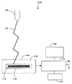
Images


Classifications
-
- G—PHYSICS
- G01—MEASURING; TESTING
- G01R—MEASURING ELECTRIC VARIABLES; MEASURING MAGNETIC VARIABLES
- G01R31/00—Arrangements for testing electric properties; Arrangements for locating electric faults; Arrangements for electrical testing characterised by what is being tested not provided for elsewhere
- G01R31/327—Testing of circuit interrupters, switches or circuit-breakers
- G01R31/3271—Testing of circuit interrupters, switches or circuit-breakers of high voltage or medium voltage devices
- G01R31/3272—Apparatus, systems or circuits therefor
- G01R31/3274—Details related to measuring, e.g. sensing, displaying or computing; Measuring of variables related to the contact pieces, e.g. wear, position or resistance
-
- G—PHYSICS
- G01—MEASURING; TESTING
- G01N—INVESTIGATING OR ANALYSING MATERIALS BY DETERMINING THEIR CHEMICAL OR PHYSICAL PROPERTIES
- G01N21/00—Investigating or analysing materials by the use of optical means, i.e. using sub-millimetre waves, infrared, visible or ultraviolet light
- G01N21/62—Systems in which the material investigated is excited whereby it emits light or causes a change in wavelength of the incident light
- G01N21/66—Systems in which the material investigated is excited whereby it emits light or causes a change in wavelength of the incident light electrically excited, e.g. electroluminescence
- G01N21/67—Systems in which the material investigated is excited whereby it emits light or causes a change in wavelength of the incident light electrically excited, e.g. electroluminescence using electric arcs or discharges
-
- H—ELECTRICITY
- H01—ELECTRIC ELEMENTS
- H01H—ELECTRIC SWITCHES; RELAYS; SELECTORS; EMERGENCY PROTECTIVE DEVICES
- H01H1/00—Contacts
- H01H1/0015—Means for testing or for inspecting contacts, e.g. wear indicator
-
- H—ELECTRICITY
- H01—ELECTRIC ELEMENTS
- H01H—ELECTRIC SWITCHES; RELAYS; SELECTORS; EMERGENCY PROTECTIVE DEVICES
- H01H33/00—High-tension or heavy-current switches with arc-extinguishing or arc-preventing means
- H01H33/70—Switches with separate means for directing, obtaining, or increasing flow of arc-extinguishing fluid
- H01H33/7015—Switches with separate means for directing, obtaining, or increasing flow of arc-extinguishing fluid characterised by flow directing elements associated with contacts
- H01H33/7076—Switches with separate means for directing, obtaining, or increasing flow of arc-extinguishing fluid characterised by flow directing elements associated with contacts characterised by the use of special materials
-
- H—ELECTRICITY
- H01—ELECTRIC ELEMENTS
- H01H—ELECTRIC SWITCHES; RELAYS; SELECTORS; EMERGENCY PROTECTIVE DEVICES
- H01H1/00—Contacts
- H01H1/0015—Means for testing or for inspecting contacts, e.g. wear indicator
- H01H2001/0026—Means for testing or for inspecting contacts, e.g. wear indicator wherein one or both contacts contain embedded contact wear signal material, e.g. radioactive material being released as soon as the contact wear reaches the embedded layer
-
- H—ELECTRICITY
- H01—ELECTRIC ELEMENTS
- H01H—ELECTRIC SWITCHES; RELAYS; SELECTORS; EMERGENCY PROTECTIVE DEVICES
- H01H1/00—Contacts
- H01H1/0015—Means for testing or for inspecting contacts, e.g. wear indicator
- H01H2001/0031—Means for testing or for inspecting contacts, e.g. wear indicator by analysing radiation emitted by arc or trace material
-
- H—ELECTRICITY
- H01—ELECTRIC ELEMENTS
- H01H—ELECTRIC SWITCHES; RELAYS; SELECTORS; EMERGENCY PROTECTIVE DEVICES
- H01H9/00—Details of switching devices, not covered by groups H01H1/00 - H01H7/00
- H01H9/0005—Tap change devices
- H01H2009/0061—Monitoring tap change switching devices
-
- H—ELECTRICITY
- H01—ELECTRIC ELEMENTS
- H01H—ELECTRIC SWITCHES; RELAYS; SELECTORS; EMERGENCY PROTECTIVE DEVICES
- H01H33/00—High-tension or heavy-current switches with arc-extinguishing or arc-preventing means
- H01H33/70—Switches with separate means for directing, obtaining, or increasing flow of arc-extinguishing fluid
- H01H33/7015—Switches with separate means for directing, obtaining, or increasing flow of arc-extinguishing fluid characterised by flow directing elements associated with contacts
- H01H33/7023—Switches with separate means for directing, obtaining, or increasing flow of arc-extinguishing fluid characterised by flow directing elements associated with contacts characterised by an insulating tubular gas flow enhancing nozzle
-
- H—ELECTRICITY
- H01—ELECTRIC ELEMENTS
- H01H—ELECTRIC SWITCHES; RELAYS; SELECTORS; EMERGENCY PROTECTIVE DEVICES
- H01H9/00—Details of switching devices, not covered by groups H01H1/00 - H01H7/00
- H01H9/0005—Tap change devices
Abstract
Description
本発明は、一般的には高圧電気機器に関する。より特定的には、本発明は、定期的に電気アークに曝される高圧電気機器の部品の摩耗の検出に関する。 The present invention relates generally to high voltage electrical equipment. More particularly, the present invention relates to detection of wear on parts of high voltage electrical equipment that are periodically exposed to an electric arc.
負荷タップ切換器、電圧調整器、回路遮断器、及びスイッチは、電力を遮断するために使用される。それらの幾つかの部品の表面は、それらの通常の動作の間に電気アーキングに定期的に曝され、また及び機械的摩擦を受けることによって腐食される。もしこれらの部品の電気的及び機械的完全性が損なわれる程度まで摩耗することを許せば、機器を故障させるようになる。最も腐食を受け易い部品は、六フッ化硫黄(SF6)ガス回路遮断器内においてアークを発生する金属接点及び「テフロン(登録商標)」ノズルである。 Load tap changers, voltage regulators, circuit breakers, and switches are used to cut off power. The surface of some of these parts is corroded by regular exposure to electrical arcing during their normal operation and subject to mechanical friction. If these parts are allowed to wear to such an extent that the electrical and mechanical integrity of the parts is compromised, the equipment will fail. The parts that are most susceptible to corrosion are metal contacts and “Teflon” nozzles that generate arcs in sulfur hexafluoride (SF 6 ) gas circuit breakers.
内部検査を行うために機器を休止させることなく、電気機器の部品が危険なまでに摩耗していることを知ることが望ましい。これを達成するために、幾つかの手法が用いられている。1つの手法は、電気機器の電気接点の中に光ファイバストランドを設けることである。接点が摩耗すると、光ファイバストランドは電気アーキングから放出される光に曝されるようになり、この光は光ファイバストランドの反対端に配置されたフォトダイオードまたは他のセンサによって検出することができる。しかし、電気接点内に光ファイバストランドを設置することは高価であり、また光ファイバストランドは機械的応力を受けると破損し易い。別の手法は、電気接点内の所定の深さに、またはSF6回路遮断器のテフロン(登録商標)ノズルの表面下にトレーサ物質を埋め込むことである。トレーサ物質が露出する点まで電気接点が摩耗すると、トレーサ物質は絶縁媒体内に解放されるか、またはそうでなければ、電気アークによって分解される。摩耗が安全レベルを越えて進行したか否かを判断するためには、絶縁媒体を定期的に採取し、トレーサ要素またはそれらの分解生成物の存在を分析しなければならない。この手法は、電気機器の連続モニタリングには適さない。 It is desirable to know that parts of electrical equipment are dangerously worn without taking the equipment out of service for internal inspection. Several approaches have been used to achieve this. One approach is to provide fiber optic strands in the electrical contacts of the electrical equipment. As the contacts wear, the fiber optic strand becomes exposed to light emitted from the electrical arcing, which light can be detected by a photodiode or other sensor located at the opposite end of the fiber optic strand. However, installing fiber optic strands in electrical contacts is expensive, and fiber optic strands are susceptible to breakage when subjected to mechanical stress. Another approach is to embed tracer material at a predetermined depth in the electrical contacts or below the surface of the Teflon nozzle of the SF 6 circuit breaker. As the electrical contact wears to the point where the tracer material is exposed, the tracer material is released into the insulating medium or otherwise decomposed by the electric arc. In order to determine whether wear has progressed beyond a safe level, the insulating medium must be periodically taken and analyzed for the presence of tracer elements or their degradation products. This method is not suitable for continuous monitoring of electrical equipment.
以上に鑑みて、電気アーキング及び機械的摩擦に曝されて腐食を受けるような電気機器部品の過度の摩耗を連続的にモニタリングする方法に対する要望が存在している。更に、新しいトレーサ物質、及びこれらの物質を分析する方法に対する要望も存在している。 In view of the foregoing, there is a need for a method for continuously monitoring excessive wear of electrical equipment components that are subject to corrosion due to electrical arcing and mechanical friction. There is also a need for new tracer materials and methods for analyzing these materials.
本発明の目的は、電気機器の部品を連続的にモニタリング(監視)することによって、それらの過大な摩耗を検出することである。 The object of the present invention is to detect excessive wear of these parts by continuously monitoring the components of the electrical equipment.
この目的及び他の目的は本発明によって達成される。本発明の一実施の形態による電気機器の部品をモニタリングする方法は、トレーサ物質が所定の深さに埋め込まれている部品を電気アークに曝すステップと、トレーサ物質が電気アークに曝されるまで部品を摩耗させるステップと、電気アークに曝された時にトレーサ物質が放出する電磁放射を検出するステップとを含む。トレーサ物質が放出する電磁放射は、部品の他のどの部分が放出する電磁放射とも異なっており、例えば、それは異なる波長を有している。トレーサ物質が放出する電磁放射を検出することによって、部品を連続的にモニタリングすることが好ましい。本発明の別の実施の形態は、電気アークを発生する可能性がある電気機器の部品を製造する方法を含む。本方法は、部品内の所定の深さにトレーサ物質を埋め込むステップを含む。 This and other objects are achieved by the present invention. A method of monitoring a component of an electrical device according to an embodiment of the present invention includes exposing a component having a tracer material embedded at a predetermined depth to an electric arc, and the component until the tracer material is exposed to the electric arc. And a step of detecting electromagnetic radiation emitted by the tracer material when exposed to an electric arc. The electromagnetic radiation emitted by the tracer material is different from the electromagnetic radiation emitted by any other part of the component, for example, it has a different wavelength. Preferably, the part is continuously monitored by detecting the electromagnetic radiation emitted by the tracer material. Another embodiment of the invention includes a method of manufacturing a component of an electrical device that can generate an electric arc. The method includes embedding a tracer material at a predetermined depth within the part.
本発明の更に別の実施の形態は、トレーサ物質が電気機器の部品内の所定の深さに埋め込まれている電気機器の摩耗を検出する装置を含む。他の実施の形態におけるように、トレーサ物質が電気アークに曝された時に放出する電磁波は、部品の他のどの部分が放出する電磁放射とも異なっており、例えば、それは異なる波長を有している。本装置は、トレーサ物質が放出する電磁放射によって部品を連続的にモニタリングするために、狭帯域幅フィルタを有するフォトダイオード、または分光光度計のような電磁検出器を含むことが好ましい。光ファイバケーブルを使用して、電磁放射を電磁検出器に伝送することもできる。適切なトレーサ物質は、リチウム、コバルト、ニオブ、及びイットリウムのような希土類金属を含む。更に、部品の摩耗の程度及び/または位置を検出するために、複数のトレーサ物質を部品内の複数の所定の深さに及び/または予め選択された位置に埋め込むことができる。 Yet another embodiment of the present invention includes an apparatus for detecting wear of an electrical device in which a tracer material is embedded at a predetermined depth within a component of the electrical device. As in other embodiments, the electromagnetic wave emitted when the tracer material is exposed to an electric arc is different from the electromagnetic radiation emitted by any other part of the component, for example, it has a different wavelength. . The apparatus preferably includes a photodiode having a narrow bandwidth filter or an electromagnetic detector such as a spectrophotometer for continuous monitoring of the component by electromagnetic radiation emitted by the tracer material. Fiber optic cables can also be used to transmit electromagnetic radiation to the electromagnetic detector. Suitable tracer materials include rare earth metals such as lithium, cobalt, niobium, and yttrium. Further, a plurality of tracer materials can be embedded at a plurality of predetermined depths and / or preselected locations within the part to detect the degree and / or position of wear of the part.
別の実施の形態において本発明は、電気機器の部品の摩耗を検出する方法を提供する。本方法は、蛍光トレーサ物質が所定の深さに埋め込まれている電気機器の部品を電気アークに曝すステップと、蛍光トレーサ物質が、部品の少なくとも一部分を取り囲む絶縁媒体内へ解放されるまで部品を摩耗させるステップと、絶縁媒体を照射し、それによって蛍光トレーサ物質に蛍光を発生させるステップと、蛍光トレーサ物質からの蛍光を検出するステップとを含む。 In another embodiment, the present invention provides a method for detecting wear of parts of an electrical device. The method includes exposing an electrical component having an embedded fluorescent tracer material to a predetermined depth to an electric arc and removing the component until the fluorescent tracer material is released into an insulating medium surrounding at least a portion of the component. Ablating, irradiating the insulating medium, thereby generating fluorescence in the fluorescent tracer material, and detecting fluorescence from the fluorescent tracer material.
別の実施の形態において、本発明は、電気アークを発生する可能性がある電気機器部品を製造する方法を提供する。本方法は、電気機器の部品内の所定の深さに蛍光トレーサ物質を埋め込むステップを含む。本発明は、更に、電気機器の摩耗を検出するシステムを提供する。このシステムは、絶縁媒体によって絶縁され、電気アークに曝される電気機器部品と、部品内の所定の深さに埋め込まれている蛍光トレーサ物質と、蛍光トレーサ物質を照射し、蛍光トレーサ物質が発生する蛍光を検出するように構成されている検出器とを含む。 In another embodiment, the present invention provides a method of manufacturing an electrical equipment component that can generate an electric arc. The method includes embedding a fluorescent tracer material at a predetermined depth within a component of an electrical device. The present invention further provides a system for detecting wear of electrical equipment. This system irradiates an electrical equipment component that is insulated by an insulating medium and exposed to an electric arc, a fluorescent tracer material that is embedded at a predetermined depth in the component, and a fluorescent tracer material to generate a fluorescent tracer material. And a detector configured to detect fluorescence.
本発明のこれらの、及び他の目的及び特色は、以下の添付図面に基づく好ましい実施の形態の説明から明白になるであろう。 These and other objects and features of the present invention will become apparent from the following description of preferred embodiments based on the accompanying drawings.
好ましい実施の形態の構造及び機能は、添付図面から最も良く理解することができよう。複数の図面に付してある同一の参照番号は、同一の、または同等の構造を示している。 The structure and function of the preferred embodiment can be best understood from the accompanying drawings. The same reference numbers in several drawings indicate the same or equivalent structures.
図1は、電気機器の部品の摩耗を検出するための本発明の実施の形態によるフローチャート100を示す。ステップ102において、所定の深さに埋め込まれているトレーサ物質を含む部品が電気アーク(アーク放電)に曝される(暴露される)。ステップ104においては、部品は、電気アークに曝された結果として、または機械的摩擦のような他の原因によって摩耗する。最後に、ステップ106において、部品はトレーサ物質からの電磁放射によって連続的にモニタリングされる。トレーサ物質は、埋め込まれているトレーサ物質自体が電気アークに曝されるようになるまで部品が十分に摩耗すると電磁放射を放出する。トレーサ物質は、部品の製造中に部品内に埋め込むことが好ましいが、部品が製造された後に完成部品内に埋め込むこともできる。
FIG. 1 shows a
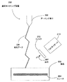
図2及び図3は、電気機器の部品202の摩耗を検出する本発明の実施の形態による装置200の概略図である。図2は初期の時点における装置200を示し、図3はより後の時点における装置200を示している。図2に示すように、電気機器(図示せず)の部品202は、所定の深さに埋め込まれているトレーサ物質204を有している。部品202は、電気アーキング要素208によって生成される電気アーク(アーク放電)206に曝される。電気アーク206の高温が、電気アーク206に曝された部品202の一部分に電磁放射207を放出させる。この電磁放射207は、電磁検出器によって連続的にモニタリングされる。電磁検出器は、フォトダイオード210、または他の何等かの適切な電磁放射検出器(例えば、分光光度計)であることができる。図2に示す実施形態においては、フォトダイオード210と電気機器の部品202との間に狭帯域フィルタ212が配置されており、フォトダイオード210は狭帯域フィルタ212を通過することができる狭帯域波長を有する電磁放射だけを検出することができる。図2に示すように、トレーサ物質204が放出したものではない電磁放射207は、狭帯域フィルタ212を通ることはできない。電磁検出器は電気機器の動作中、連続的に電気機器の部品202をモニタリングすることができる。
2 and 3 are schematic views of an
図3は、図2と同じ装置200の概略図であるが、部品202が摩耗した後の時点における状態を示している。図2とは対照的に、図3においてはトレーサ物質202は部品202内の所定の深さに埋没しておらず、代わりに部品202の表面上に露出している。図3に示すようなより後の時点では、部品202の表面は電気アーク206に曝された結果として、または機械的摩擦のような他の原因による摩耗で除去され、トレーサ物質204が電気アーク206に曝される。電気アーク206の高温が、トレーサ物質204に電磁放射209を放出させる。トレーサ物質204は、電気アーク206に曝された時に、同じく電気アークに曝される部品の他のどの部分が放出する電磁放射207(図2)とも異なる電磁放射209を放出するように選択される。例えば、幾つかの用途においては、約670.7nmの波長に対応する赤色光を放出するリチウムが適切なトレーサ物質であろう。トレーサ物質204は、部品の動作状態の下で化学的及び熱的に安定であることが望ましい。トレーサ物質204はまた、電気機器内で使用されるどのような流体媒体の誘電特性にも影響しないことが望ましい。本発明によるトレーサ物質として使用に適する材料には、リチウム、コバルト、ニオブ、及び、イットリウムのような希土類金属が含まれる。図3に示すように、電磁放射209はトレーサ物質204が放出したものであるから、狭帯域フィルタ212を通過して伝達される。
FIG. 3 is a schematic view of the
図2及び図3に示す実施の形態においては、トレーサ物質が電気アーク206に曝された時に放出する電磁放射は、狭帯域フィルタ212を通過した後にフォトダイオード210によって検出される。狭帯域フィルタ212は、それが伝達する狭い帯域の外側の波長を有する電磁放射を除去する。狭帯域フィルタ212は、トレーサ物質が電気アークに曝された時に放出する電磁放射は透過させるが、部品202の他の部分から放出される電磁放射は透過させないように選択されている。
In the embodiment shown in FIGS. 2 and 3, the electromagnetic radiation emitted when the tracer material is exposed to the
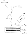
図4は、電気機器の部品202の2つの摩耗の量を検出する本発明の代替実施の形態による装置400の概略図である。図4に示すように、第1のトレーサ物質402が部品202内の1つの深さに埋め込まれ、第2のトレーサ物質404が部品202内の別の深さに埋め込まれている。第1のトレーサ物質402及び第2のトレーサ物質404は、それらが電気アーク206に曝された時に、互いに異なる、且つ電気アークに曝される部品の他のどの部分が放出する放射とも異なる電磁放射を放出するように選択されている。分光光度計406は、部品202からの電磁放射を分析し、部品202の表面が第1のトレーサ物質402を露出させるまで摩耗したのか、または第2のトレーサ物質404を露出させるまで摩耗したのかを決定する。代替として、異なる狭帯域フィルタを有する2つのフォトダイオードを使用し、第1のトレーサ物質402及び第2のトレーサ物質404からの電磁放射をモニタリングすることができる。どのトレーサ物質が電気アーク206に曝されているかによって部品202の摩耗の程度及び/または位置を推定するために、付加的なトレーサ物質(図示せず)を部品202の異なる深さ及び/または異なる位置に埋め込むことができる。
FIG. 4 is a schematic diagram of an
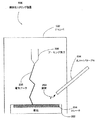
図5は、電気機器の部品202の摩耗を検出する本発明の代替実施の形態による装置500の概略図である。図5に示す実施形態においては、アーキング要素208、及び埋め込まれたトレーサ物質204を有する部品202がチャンバ502内に配置され、部品が放出する電磁放射を機器チャンバ502の外部の電磁検出器(図示せず)に伝送するために光ファイバケーブル504が使用されている。
FIG. 5 is a schematic view of an
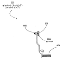
以下に説明する本発明の使用実施例は本発明の範囲を制限するものではなく、単なる例示するためのものに過ぎない。以下の実施例は、負荷タップ切換器及び回路遮断器の摩耗を検出する本発明による装置に関連している。本発明を使用することができると考えられる他の機器には、電圧調整器、及びSF6ガス遮断器が含まれる。 The following examples of use of the invention are not intended to limit the scope of the invention, but are merely exemplary. The following example relates to a device according to the invention for detecting wear of load tap changers and circuit breakers. Other equipment that could be used with the present invention includes voltage regulators and SF 6 gas circuit breakers.
図6は、本発明の実施の形態による負荷タップ切換器のダイバータスイッチアセンブリ600の断面図である。ダイバータスイッチアセンブリ600は、その一方の端にアーキングコンタクトチップアセンブリ602と、その反対端に圧縮バネ604を含む。アーキングコンタクトチップアセンブリ602は、エルコナイト接点606を含むことができる。図6に示すように、トレーサ物質608はエルコナイト接点606内に埋め込まれている。本発明によれば、エルコナイト接点606の表面が摩耗によって除去されると、トレーサ物質608が電気アーク(図示せず)に曝されるようになり、電磁検出器(図示せず)はトレーサ物質608が放出する識別可能な電磁放射を検出することになる。
FIG. 6 is a cross-sectional view of a
図7、図8、及び図9は、それぞれ、本発明の実施の形態による回路遮断器700、回路遮断器700の固定接点アセンブリ702、及び回路遮断器700の可動接点アセンブリ708の部分切除断面図である。図7は、固定接点ピン706を有する固定接点アセンブリ702、タンク704、及び可動接点アセンブリ708を含む回路遮断器700を示す。
7, 8, and 9 are partially cutaway sectional views of a
図8は、シールディング710、多接点ライナ及び締付けリング712、接点ピンホールダ714、絶縁支持具716、接点クラウン718、及び固定接点ピン706を含む回路遮断器700の固定接点アセンブリ702を示す。図8に示すように、トレーサ物質720は固定接点ピン706内に埋め込まれている。本発明によれば、トレーサ物質720は、固定接点ピン706の表面が摩耗して除去されると電気アーク(図示せず)に曝され始め、電磁検出器(図示せず)はトレーサ物質720が放出する識別可能な電磁放射を検出するようになる。
FIG. 8 shows a
図9に、主接点722を含む回路遮断器700の可動接点アセンブリ708を示す。
図9に示すように、トレーサ物質724及び726は、主接点722内に埋め込まれている。本発明によれば、トレーサ物質724及び726は、主接点722の表面が摩耗して除去されると電気アーク(図示せず)に曝され始め、電磁検出器(図示せず)はトレーサ物質724及び726が放出する識別可能な電磁放射を検出するようになる。
FIG. 9 illustrates a
As shown in FIG. 9,
図10は、電気機器の部品の摩耗を検出する本発明の別の実施の形態による装置1000の概略図である。この実施の形態においては、トレーサ物質1010は蛍光物質からなる。蛍光物質は、電気機器の部品1020内の所定の深さに埋め込まれている。この実施の形態は、好ましくは、部品1020が鉱油のような絶縁媒体1030内に浸漬される場合に使用する。絶縁媒体は部品1020を取り囲むことが好ましく、容器1040内に、または部品1020が存在している電気機器内に収容される。部品が十分に摩耗すると蛍光トレーサ物質1010が露出し始め、絶縁媒体1030内に解放される。図10に示すように、部品1020の摩耗は、アーキング要素208から放電するアーク206の結果であるか、または機械的摩擦の結果であり得る。
FIG. 10 is a schematic diagram of an
蛍光トレーサ物質1010が解放され、絶縁媒体1030が照射または照明されると、蛍光トレーサ物質1010が励起されて蛍光を発生する。この実施の形態においては、プローブ1050が容器1040内に、または絶縁媒体1030を保持している電気機器内に配置されており、放射または励起光を絶縁媒体1030へ供給するために使用されている。放射、即ち電磁放射の源1075が、例えば光ファイバ1070によってプローブ1050に結合され、プローブ1050は絶縁媒体1030へ放射を供給する。放射源1075は、絶縁媒体1030内の蛍光トレーサ物質1010が蛍光を発生するのに必要な波長に対応する所望の波長を有するどのような光、または放射の源であることもできる。蛍光の波長は、蛍光トレーサ物質を照射または照明するために使用する光とは異なっていることが好ましい。
When the
プローブ1050からの放射によって照射または照明された蛍光トレーサ物質1010が発生した蛍光は、同じプローブ1050によって検出される。この場合、プローブ1050は、蛍光を連続的にモニタリングして検出することができる光センサ、フォトダイオード、または他の適切なデバイスのような検出器1055を含む。絶縁媒体1030内の照射された蛍光トレーサ物質1010が発生する特定の蛍光を選択的にモニタリングするために、フィルタのような他の光学素子を検出器1055と共に使用できることが理解されよう。検出器1055は、電気コネクタ1060によって記録装置1065に接続されている。記録装置1065は、検出器1055が発生した信号を記録し、分析して蛍光トレーサ物質1010が絶縁媒体1030内へ解放されたか否かを決定し、それによって部品1020の摩耗が所定の量まで進行したことを指示する。代替として、検出器1055は単なる光ファイバの端であることができる。この光ケーブルは、受信した光を分光光度計のような光モニタリング装置へ伝送して分析させる。
The fluorescence generated by the
この実施の形態においては、プローブを絶縁媒体1030内に恒久的に位置決めし、絶縁媒体内へ解放された蛍光トレーサ物質をその場所において照射し、連続的に、半連続的に、または必要に応じて、蛍光をその場所において検出することができることを理解されたい。蛍光は、蛍光を検出する時にアークがもたらす干渉を最小にするために、アークが存在しない時に検出することが好ましい。代替として、必要な時だけプローブ1050を容器1040内へ挿入することができるように構成することができる。また、検出器1055から、または分光光度計のような光モニタリング装置から供給される信号を、データ記憶及び分析のためにコンピュータへ送給できることも理解されたい。更に、蛍光トレーサ物質を部品内の何れかの所望の深さに使用し、同一部品内の1箇所以上の深さに配置して部品の劣化の速度に関する情報を得たり、部品が摩耗するにつれて複数の指示を供給したりできることをも理解されたい。
In this embodiment, the probe is permanently positioned in the insulating
蛍光トレーサ物質自体は、それを取り囲む絶縁媒体内に溶解、または分散する物質であれば、どのような蛍光物質であってもよい。蛍光トレーサ物質は、それを取り囲む絶縁媒体内に溶解または分散した時に、絶縁媒体内の蛍光トレーサ物質が低濃度であっても蛍光を検出することができるように十分な蛍光を発生することが好ましい。一実施の形態においては、蛍光物質からの蛍光は、絶縁媒体内の蛍光物質の濃度が約0.5ppbであっても検出可能であることが好ましい。光またはエネルギ源から励起された時の蛍光トレーサ物質が、励起光(紫外または可視光のような)の波長よりも常に長い波長を有する光(即ち、蛍光)を放出することが好ましい。絶縁媒体が油である場合には油からの干渉を最小にするために、スペクトルの赤領域内の光または蛍光を放出する蛍光トレーサ物質を選択することが望ましい。 The fluorescent tracer material itself may be any fluorescent material that dissolves or disperses in the insulating medium surrounding it. The fluorescent tracer material preferably generates sufficient fluorescence when dissolved or dispersed in the insulating medium surrounding it so that the fluorescence can be detected even at low concentrations of the fluorescent tracer material in the insulating medium. . In one embodiment, the fluorescence from the fluorescent material is preferably detectable even when the concentration of the fluorescent material in the insulating medium is about 0.5 ppb. It is preferred that the fluorescent tracer material when excited from a light or energy source emit light having a wavelength that is always longer than the wavelength of the excitation light (such as ultraviolet or visible light) (ie, fluorescence). When the insulating medium is oil, it is desirable to select a fluorescent tracer material that emits light or fluorescence in the red region of the spectrum to minimize interference from the oil.
蛍光物質の組成は、有機染料であることができる。どのような適切な有機染料も使用することができる。有機染料は、粉末であることも、または有機染料粉末を含む液体であることもできる。もし有機染料が液体の形状であればその液体を容器内に密封し、容器を電気部品内に埋め込むことができる。しかしながら、この容器が露出した時には、取り囲む絶縁媒体内に有機染料を溶解、または分散させることができるように破裂可能でなければならない。有機染料は、油のような絶縁媒体内への高い溶解度を有し、良好な化学的及び熱的安定度を有し、例えば約150℃よりも高い沸点を有し、そして高レベルの蛍光を発生する能力を有しているものが好ましい。一実施の形態においては、有機染料は、例えば絶縁媒体内に溶け易く、沈降しないアゾ染料を含む溶剤染料である。 The composition of the fluorescent material can be an organic dye. Any suitable organic dye can be used. The organic dye can be a powder or a liquid containing an organic dye powder. If the organic dye is in liquid form, the liquid can be sealed in the container and the container can be embedded in the electrical component. However, when the container is exposed, it must be burstable so that the organic dye can be dissolved or dispersed in the surrounding insulating medium. Organic dyes have high solubility in insulating media such as oils, have good chemical and thermal stability, have boiling points higher than, for example, about 150 ° C., and high levels of fluorescence. Those having the ability to generate are preferred. In one embodiment, the organic dye is, for example, a solvent dye that includes an azo dye that is readily soluble in the insulating medium and does not settle.
蛍光物質は、無機ナノクリスタル粉末であることもできる。好ましくは、無機ナノクリスタル粉末は、約2から10nmまでの、好ましくは約4から5nmまでの範囲内の粒子サイズの半導体ナノクリスタル量子ドットである。これらの型のナノクリスタルは、典型的に、狭帯域内において高い蛍光強度を呈し、化学的及び熱的に極めて安定であり、退色に対して耐性があり、広帯域の源を用いて励起することができる。好ましい実施の形態においては、ナノクリスタル粉末は、Evident Technologyから入手可能なEVIDOTSのようなカドミウム・テルル/硫化カドミウム、またはカドミウム・セレン/硫化亜鉛であることができる。これらの特定のナノクリスタルもスペクトルの赤領域において光を放出し、油のような絶縁媒体からの干渉を受け難い。 The fluorescent material can also be an inorganic nanocrystal powder. Preferably, the inorganic nanocrystal powder is a semiconductor nanocrystal quantum dot with a particle size in the range of about 2 to 10 nm, preferably about 4 to 5 nm. These types of nanocrystals typically exhibit high fluorescence intensity within a narrow band, are extremely chemically and thermally stable, resistant to fading, and can be excited using a broadband source Can do. In preferred embodiments, the nanocrystal powder can be cadmium tellurium / cadmium sulfide, such as EVIDOTS available from Evident Technology, or cadmium selenium / zinc sulfide. These particular nanocrystals also emit light in the red region of the spectrum and are less susceptible to interference from insulating media such as oil.
図11は、電気機器の部品の摩耗を検出する本発明の更に別の実施の形態による装置1100の概略図である。図10におけるように、トレーサ物質1110は、部品1120内の所定の深さに埋め込まれている蛍光物質からなる。部品1120は、容器1140内に容れられている鉱油のような絶縁媒体1130内に浸漬されている。アーキング要素208から放電する電気アーク206の結果として、または機械的摩擦によって部品1120が十分に摩耗すると、蛍光トレーサ物質1110が露出して絶縁媒体1130内へ解放され始める。蛍光トレーサ物質は、図10に関して説明したようなどのような物質であることもできる。しかしながら、この実施の形態においては、取り囲む絶縁媒体1130内へ解放された蛍光トレーサ物質1110の照射または励起、及びその結果として発生する蛍光の検出は電気部品及び装置の外部において遂行される。
FIG. 11 is a schematic diagram of an
詳述すれば、部品を取り囲む絶縁媒体は、試料セルに流体的に結合されている。これによって絶縁媒体1130の試料が容器1140から採取され、分析のために試料セル1170へ送られる。サンプリング速度及び量は、コンピュータによって制御できることは理解されよう。
Specifically, the insulating medium surrounding the part is fluidly coupled to the sample cell. As a result, a sample of the insulating
試料セル1170内の試料は、放射、即ち電磁源1150からの放射(その波長は、特定の蛍光トレーサ物質が蛍光を発生する波長に対応する)によって照射または励起される。結果として発生する蛍光を検出するために、分光光度計または類似の分析装置のような検出器1160を使用することができる。試料は、普通は、照射及び検出の後に排出ライン1180を通して破棄される。サンプリングが、必要に応じて(半連続的に、または連続的にを含む)行われることは理解されよう。サンプリングされる絶縁媒体の量は一般的には数ミリリットルにしか過ぎないが、採取の頻度に依存して、部品を取り囲む絶縁媒体に付加的な絶縁媒体を追加する必要があるかも知れない。代替として、試料は部品を取り囲む絶縁媒体へ戻すことができるが、この場合、戻された残留蛍光トレーサ物質を補償するために、次の試料を励起する前に基底信号または背景信号を確立しておくべきである。
The sample in
図10と同様に、収集されたデータを記憶し、分析するために、検出器1160をコンピュータに結合することができることは理解されよう。また、絶縁媒体のサンプリングを手動で行い、部品を取り囲む絶縁媒体に試料セルを流体的に結合する必要性を回避できることも理解されよう。 It will be appreciated that, similar to FIG. 10, detector 1160 can be coupled to a computer for storing and analyzing the collected data. It will also be appreciated that the sampling of the insulating medium can be performed manually, avoiding the need to fluidly couple the sample cell to the insulating medium surrounding the part.
本発明の幾つかの実施の形態を説明したが、この説明は、単に本発明の例示に過ぎない。当業者には、特許請求の範囲内に記載されている本発明に変更を加え得ることが明らかであろう。例えば、電磁放射検出器の例としてフォトダイオードを狭帯域フィルタと共に用いるように説明したが、他の何等かの適切な電磁放射検出器を本発明に使用できることが理解されよう。更に、本発明を負荷タップ切換器及び回路遮断器の特定例を用いて説明したが、電気アークに曝される電気機器のどのような部品も本発明の範囲内にあるものと理解されたい。 Although several embodiments of the present invention have been described, this description is merely illustrative of the invention. It will be apparent to those skilled in the art that modifications may be made to the invention as described in the claims. For example, while a photodiode has been described as an example of an electromagnetic radiation detector for use with a narrow band filter, it will be understood that any other suitable electromagnetic radiation detector can be used in the present invention. Further, although the present invention has been described with specific examples of load tap changers and circuit breakers, it should be understood that any component of electrical equipment that is exposed to an electric arc is within the scope of the present invention.
以上の説明及び図面は本発明の好ましい実施の形態に関しているが、特許請求の範囲に記載されている本発明の思想及び範囲から逸脱することなく、種々の追加、変更、及び置換を考案できることは理解されよう。特に、当業者ならば、本発明をその思想または必須の特色から逸脱することなく他の要素、材料、及び構成部品を用いて他の特定の形態、構造、配列、及び比率で実現できることは理解されよう。従って、上述した実施の形態は全ての点において限定的ではなく例示的であり、本発明の範囲が上記説明に限定されるものではなく、特許請求の範囲によってのみ限定されることを理解されたい。 Although the foregoing description and drawings relate to preferred embodiments of the present invention, it is possible to devise various additions, modifications, and substitutions without departing from the spirit and scope of the present invention described in the claims. It will be understood. In particular, one of ordinary skill in the art appreciates that the present invention can be implemented in other specific forms, structures, arrangements, and proportions using other elements, materials, and components without departing from its spirit or essential characteristics. Let's be done. Therefore, it should be understood that the above-described embodiments are illustrative rather than restrictive in all respects, and the scope of the present invention is not limited to the above description, but is limited only by the claims. .
200 摩耗検出装置
202 電気機器の部品
204 トレーサ物質
206 電気アーク
207、209 電磁放射
208 アーキング要素
210 フォトダイオード
212 狭帯域フィルタ
400 摩耗検出装置
402 第1のトレーサ物質
404 第2のトレーサ物質
406 分光光度計
500 摩耗検出装置
502 チャンバ
504 光ファイバケーブル
600 ダイバータスイッチアセンブリ
602 アーキングコンタクトチップアセンブリ
604 圧縮ばね
606 エルコナイト接点
608 トレーサ物質
700 回路遮断器
702 固定接点アセンブリ
704 タンク
706 固定接点ピン
708 可動接点アセンブリ
710 シールディング
712 多接点ライナ及び締付けリング
714 接点ピンホールダ
716 絶縁支持具
718 接点クラウン
720、724、726 トレーサ物質
722 主接点
1000、1100 摩耗検出装置
1010、1110 トレーサ物質
1020、1120 電気機器の部品
1030、1130 絶縁媒体
1040、1140 容器
1050 プローブ
1055、1160 検出器
1060 コネクタ
1065 記録装置
1070 光ファイバ
1075、1150 電磁放射の源
1170 試料セル
1180 排出ライン
200
Claims (13)
蛍光トレーサ物質が所定の深さに埋め込まれている電気機器の部品を電気アークに曝すステップと、
前記蛍光トレーサ物質を、前記部品の少なくとも一部分を取り囲む絶縁媒体内に解放させるように前記部品を摩耗させるステップと、
前記絶縁媒体を照射し、それによって前記蛍光トレーサ物質に蛍光を発生させるステップと、
前記蛍光トレーサ物質からの蛍光を検出するステップと、
を含むことを特徴とする方法。 A method for detecting wear of parts of electrical equipment,
Exposing a component of an electrical device in which a fluorescent tracer material is embedded at a predetermined depth to an electric arc;
Abrading the part to release the fluorescent tracer material into an insulating medium surrounding at least a portion of the part;
Irradiating the insulating medium, thereby generating fluorescence in the fluorescent tracer material;
Detecting fluorescence from the fluorescent tracer material;
A method comprising the steps of:
前記機器の部品内の所定の深さに蛍光トレーサ物質を埋め込むステップ、
を含むことを特徴とする方法。 A method of manufacturing a part of an electrical device that can generate an electric arc, comprising:
Embedding a fluorescent tracer material at a predetermined depth within a component of the device;
A method comprising the steps of:
絶縁媒体によって絶縁され、電気アークに曝される電気機器の部品と、
前記部品内の所定の深さに埋め込まれている蛍光トレーサ物質と、
前記蛍光トレーサ物質を照射し、前記蛍光トレーサ物質が発生する蛍光を検出するように構成されている検出器と、
を含むことを特徴とするシステム。 A system for detecting wear of electrical equipment,
Parts of electrical equipment insulated by an insulating medium and exposed to an electric arc;
A fluorescent tracer material embedded at a predetermined depth in the part;
A detector configured to irradiate the fluorescent tracer material and detect fluorescence generated by the fluorescent tracer material;
A system characterized by including.
Applications Claiming Priority (1)
| Application Number | Priority Date | Filing Date | Title |
|---|---|---|---|
| US10/917,747 US7053625B2 (en) | 2002-09-11 | 2004-08-13 | Method and apparatus for detecting wear in components of high voltage electrical equipment |
Publications (2)
| Publication Number | Publication Date |
|---|---|
| JP2006054188A true JP2006054188A (en) | 2006-02-23 |
| JP2006054188A5 JP2006054188A5 (en) | 2006-05-25 |
Family
ID=35311765
Family Applications (1)
| Application Number | Title | Priority Date | Filing Date |
|---|---|---|---|
| JP2005235462A Pending JP2006054188A (en) | 2004-08-13 | 2005-08-15 | Method and apparatus for detecting wear of component of high voltage electric equipment |
Country Status (7)
| Country | Link |
|---|---|
| US (1) | US7053625B2 (en) |
| EP (1) | EP1626268B1 (en) |
| JP (1) | JP2006054188A (en) |
| AT (1) | ATE430307T1 (en) |
| AU (1) | AU2005203543B2 (en) |
| CA (1) | CA2515618A1 (en) |
| DE (1) | DE602005014178D1 (en) |
Cited By (2)
| Publication number | Priority date | Publication date | Assignee | Title |
|---|---|---|---|---|
| CN102735976A (en) * | 2012-07-05 | 2012-10-17 | 金施特·尼古拉·弗拉基米罗维奇 | Monitoring method for state of elements of high voltage electric power equipment |
| JP2013105007A (en) * | 2011-11-14 | 2013-05-30 | Ricoh Co Ltd | Photoreceptor, process cartridge, and image forming apparatus |
Families Citing this family (7)
| Publication number | Priority date | Publication date | Assignee | Title |
|---|---|---|---|---|
| US7038201B2 (en) * | 2002-12-13 | 2006-05-02 | Nichols Applied Technology, Llc | Method and apparatus for determining electrical contact wear |
| JP5032091B2 (en) * | 2006-10-12 | 2012-09-26 | 株式会社東芝 | Gas insulated switchgear and arc damage detection method for gas insulated switchgear parts |
| CN102017349B (en) * | 2008-04-21 | 2014-01-15 | Abb研究有限公司 | Arc detector and associated method for detecting undesired arcs |
| US9329238B1 (en) * | 2014-11-14 | 2016-05-03 | Schneider Electric USA, Inc. | Contact wear detection by spectral analysis shift |
| CN104827490B (en) * | 2015-05-21 | 2016-07-06 | 大连理工大学 | Based on tactile sensing device of robot's system and method that friction or electrostatic induction control |
| US9885659B1 (en) | 2016-10-04 | 2018-02-06 | International Business Machines Corporation | Method to determine connector metal wear via flouresence |
| US11181462B2 (en) | 2018-11-30 | 2021-11-23 | International Business Machines Corporation | Non-destructive method to determine porosity in metallic coatings |
Family Cites Families (11)
| Publication number | Priority date | Publication date | Assignee | Title |
|---|---|---|---|---|
| US3164006A (en) * | 1962-04-16 | 1965-01-05 | James R Alburger | Evaluation performance of liquid penetrant tracer materials |
| US3715598A (en) * | 1969-06-12 | 1973-02-06 | G Tomlin | Integral fault detection system for operating electronics equipment |
| US5389792A (en) * | 1993-01-04 | 1995-02-14 | Grumman Aerospace Corporation | Electron microprobe utilizing thermal detector arrays |
| US5453591A (en) * | 1994-04-05 | 1995-09-26 | Abb Power T&D Company Inc. | Sensing structure for component wear in high voltage circuit interrupters |
| JPH07333369A (en) * | 1994-06-13 | 1995-12-22 | Hitachi Ltd | Nuclear fusion system |
| EP0787305B1 (en) * | 1994-10-27 | 1998-05-13 | Siemens Aktiengesellschaft | Switching device with monitoring the wear of at least one contact |
| US5941370A (en) * | 1996-09-10 | 1999-08-24 | Nichols; Bruce W. | Electrical contact wear |
| DE19936868A1 (en) * | 1999-08-05 | 2001-02-15 | Patent Treuhand Ges Fuer Elektrische Gluehlampen Mbh | Method and device for producing oxidic nanocrystals |
| US6448758B1 (en) * | 2000-01-07 | 2002-09-10 | General Electric Company | Method for determining wear and other characteristics of electrodes in high voltage equipment |
| US6777948B2 (en) * | 2002-09-11 | 2004-08-17 | Electric Power Research Institute, Inc. | Method and apparatus for detecting wear in components of high voltage electrical equipment |
| US6884998B2 (en) * | 2002-12-13 | 2005-04-26 | Nichols Applied Technology, Llc | Method and apparatus for determining electrical contact wear |
-
2004
- 2004-08-13 US US10/917,747 patent/US7053625B2/en not_active Expired - Fee Related
-
2005
- 2005-08-06 DE DE602005014178T patent/DE602005014178D1/en active Active
- 2005-08-06 AT AT05254930T patent/ATE430307T1/en not_active IP Right Cessation
- 2005-08-06 EP EP05254930A patent/EP1626268B1/en not_active Not-in-force
- 2005-08-08 CA CA002515618A patent/CA2515618A1/en not_active Abandoned
- 2005-08-09 AU AU2005203543A patent/AU2005203543B2/en not_active Ceased
- 2005-08-15 JP JP2005235462A patent/JP2006054188A/en active Pending
Cited By (2)
| Publication number | Priority date | Publication date | Assignee | Title |
|---|---|---|---|---|
| JP2013105007A (en) * | 2011-11-14 | 2013-05-30 | Ricoh Co Ltd | Photoreceptor, process cartridge, and image forming apparatus |
| CN102735976A (en) * | 2012-07-05 | 2012-10-17 | 金施特·尼古拉·弗拉基米罗维奇 | Monitoring method for state of elements of high voltage electric power equipment |
Also Published As
| Publication number | Publication date |
|---|---|
| CA2515618A1 (en) | 2006-02-13 |
| EP1626268A3 (en) | 2007-12-26 |
| DE602005014178D1 (en) | 2009-06-10 |
| US7053625B2 (en) | 2006-05-30 |
| EP1626268B1 (en) | 2009-04-29 |
| US20050104598A1 (en) | 2005-05-19 |
| AU2005203543A1 (en) | 2006-03-02 |
| ATE430307T1 (en) | 2009-05-15 |
| AU2005203543B2 (en) | 2008-02-07 |
| EP1626268A2 (en) | 2006-02-15 |
Similar Documents
| Publication | Publication Date | Title |
|---|---|---|
| JP2006054188A (en) | Method and apparatus for detecting wear of component of high voltage electric equipment | |
| US7368743B2 (en) | Device for detecting fluorescent trace material | |
| CN105675587B (en) | Electrical equipment online supervision method and device based on laser induced breakdown spectroscopy | |
| Loiselle et al. | Comparative studies of the stability of various fluids under electrical discharge and thermal stresses | |
| KR102256458B1 (en) | Determination of oil degradation using fluorescence rise-time | |
| US8702304B2 (en) | Temperature indicators utilizing trace materials | |
| AU2003270071B2 (en) | Method and apparatus for detecting wear in components of high voltage electrical equipment | |
| Parvin et al. | Simultaneous fluorescence and breakdown spectroscopy of fresh and aging transformer oil immersed in paper using ArF excimer laser | |
| Dominelli et al. | Life extension and condition assessment: techniques for an aging utility infrastructure | |
| US9068892B2 (en) | Method for the emission analysis of the elemental composition of liquid media | |
| CN115825614A (en) | Transformer aging diagnosis method based on insulating oil color development technology | |
| Li | Study of dissolved gas analysis under electrical and thermal stresses for natural esters used in power transformers | |
| Fauzi et al. | Detection of power transformer fault conditions using optical characteristics of transformer oil | |
| Alshehawy et al. | Photoluminescence based condition assessment of aged transformer oil | |
| KR102601867B1 (en) | Life evaluation apparatus of transformer | |
| Yan | Portable Optical Probe for Monitoring of Transformer Oils | |
| Neettiyath et al. | Optical Sensing Techniques for Condition Monitoring of Transformer Insulation Material | |
| Liphard | A nanosecond temperature‐jump apparatus for high pressures | |
| FR2731520A1 (en) | Method for measuring electrical arc current intensity in sulphur hexa:fluoride switching device | |
| BE1015940A3 (en) | Process for analyzing a fused material by optical emission spectrometry comprises using a sensitive element with an excitation unit to excite the material being analyzed | |
| Aparna et al. | Laser Induced Breakdown Spectroscopy to detect copper contamination in transformer insulation | |
| KR100825590B1 (en) | Measuring method for inclusions`s oxygen of molten iron | |
| Hwang et al. | Relationship between initial thermal characteristics and lifetime projection of semiconductor laser diodes |
Legal Events
| Date | Code | Title | Description |
|---|---|---|---|
| A521 | Request for written amendment filed |
Free format text: JAPANESE INTERMEDIATE CODE: A523 Effective date: 20060314 |
|
| A131 | Notification of reasons for refusal |
Free format text: JAPANESE INTERMEDIATE CODE: A131 Effective date: 20080204 |
|
| A601 | Written request for extension of time |
Free format text: JAPANESE INTERMEDIATE CODE: A601 Effective date: 20080502 |
|
| A602 | Written permission of extension of time |
Free format text: JAPANESE INTERMEDIATE CODE: A602 Effective date: 20080509 |
|
| A02 | Decision of refusal |
Free format text: JAPANESE INTERMEDIATE CODE: A02 Effective date: 20081020 |