JP2005534971A - Array device with switching circuit having bootslap capacitor - Google Patents
Array device with switching circuit having bootslap capacitor Download PDFInfo
- Publication number
- JP2005534971A JP2005534971A JP2004525666A JP2004525666A JP2005534971A JP 2005534971 A JP2005534971 A JP 2005534971A JP 2004525666 A JP2004525666 A JP 2004525666A JP 2004525666 A JP2004525666 A JP 2004525666A JP 2005534971 A JP2005534971 A JP 2005534971A
- Authority
- JP
- Japan
- Prior art keywords
- pixel
- switching
- switching transistor
- signal
- voltage
- Prior art date
- Legal status (The legal status is an assumption and is not a legal conclusion. Google has not performed a legal analysis and makes no representation as to the accuracy of the status listed.)
- Withdrawn
Links
Images


Classifications
-
- G—PHYSICS
- G02—OPTICS
- G02F—OPTICAL DEVICES OR ARRANGEMENTS FOR THE CONTROL OF LIGHT BY MODIFICATION OF THE OPTICAL PROPERTIES OF THE MEDIA OF THE ELEMENTS INVOLVED THEREIN; NON-LINEAR OPTICS; FREQUENCY-CHANGING OF LIGHT; OPTICAL LOGIC ELEMENTS; OPTICAL ANALOGUE/DIGITAL CONVERTERS
- G02F1/00—Devices or arrangements for the control of the intensity, colour, phase, polarisation or direction of light arriving from an independent light source, e.g. switching, gating or modulating; Non-linear optics
- G02F1/01—Devices or arrangements for the control of the intensity, colour, phase, polarisation or direction of light arriving from an independent light source, e.g. switching, gating or modulating; Non-linear optics for the control of the intensity, phase, polarisation or colour
- G02F1/13—Devices or arrangements for the control of the intensity, colour, phase, polarisation or direction of light arriving from an independent light source, e.g. switching, gating or modulating; Non-linear optics for the control of the intensity, phase, polarisation or colour based on liquid crystals, e.g. single liquid crystal display cells
- G02F1/133—Constructional arrangements; Operation of liquid crystal cells; Circuit arrangements
-
- G—PHYSICS
- G09—EDUCATION; CRYPTOGRAPHY; DISPLAY; ADVERTISING; SEALS
- G09G—ARRANGEMENTS OR CIRCUITS FOR CONTROL OF INDICATING DEVICES USING STATIC MEANS TO PRESENT VARIABLE INFORMATION
- G09G3/00—Control arrangements or circuits, of interest only in connection with visual indicators other than cathode-ray tubes
- G09G3/20—Control arrangements or circuits, of interest only in connection with visual indicators other than cathode-ray tubes for presentation of an assembly of a number of characters, e.g. a page, by composing the assembly by combination of individual elements arranged in a matrix no fixed position being assigned to or needed to be assigned to the individual characters or partial characters
- G09G3/34—Control arrangements or circuits, of interest only in connection with visual indicators other than cathode-ray tubes for presentation of an assembly of a number of characters, e.g. a page, by composing the assembly by combination of individual elements arranged in a matrix no fixed position being assigned to or needed to be assigned to the individual characters or partial characters by control of light from an independent source
- G09G3/36—Control arrangements or circuits, of interest only in connection with visual indicators other than cathode-ray tubes for presentation of an assembly of a number of characters, e.g. a page, by composing the assembly by combination of individual elements arranged in a matrix no fixed position being assigned to or needed to be assigned to the individual characters or partial characters by control of light from an independent source using liquid crystals
- G09G3/3611—Control of matrices with row and column drivers
- G09G3/3648—Control of matrices with row and column drivers using an active matrix
-
- G—PHYSICS
- G09—EDUCATION; CRYPTOGRAPHY; DISPLAY; ADVERTISING; SEALS
- G09G—ARRANGEMENTS OR CIRCUITS FOR CONTROL OF INDICATING DEVICES USING STATIC MEANS TO PRESENT VARIABLE INFORMATION
- G09G2300/00—Aspects of the constitution of display devices
- G09G2300/08—Active matrix structure, i.e. with use of active elements, inclusive of non-linear two terminal elements, in the pixels together with light emitting or modulating elements
- G09G2300/0809—Several active elements per pixel in active matrix panels
-
- G—PHYSICS
- G09—EDUCATION; CRYPTOGRAPHY; DISPLAY; ADVERTISING; SEALS
- G09G—ARRANGEMENTS OR CIRCUITS FOR CONTROL OF INDICATING DEVICES USING STATIC MEANS TO PRESENT VARIABLE INFORMATION
- G09G3/00—Control arrangements or circuits, of interest only in connection with visual indicators other than cathode-ray tubes
- G09G3/20—Control arrangements or circuits, of interest only in connection with visual indicators other than cathode-ray tubes for presentation of an assembly of a number of characters, e.g. a page, by composing the assembly by combination of individual elements arranged in a matrix no fixed position being assigned to or needed to be assigned to the individual characters or partial characters
- G09G3/34—Control arrangements or circuits, of interest only in connection with visual indicators other than cathode-ray tubes for presentation of an assembly of a number of characters, e.g. a page, by composing the assembly by combination of individual elements arranged in a matrix no fixed position being assigned to or needed to be assigned to the individual characters or partial characters by control of light from an independent source
- G09G3/36—Control arrangements or circuits, of interest only in connection with visual indicators other than cathode-ray tubes for presentation of an assembly of a number of characters, e.g. a page, by composing the assembly by combination of individual elements arranged in a matrix no fixed position being assigned to or needed to be assigned to the individual characters or partial characters by control of light from an independent source using liquid crystals
- G09G3/3611—Control of matrices with row and column drivers
- G09G3/3648—Control of matrices with row and column drivers using an active matrix
- G09G3/3659—Control of matrices with row and column drivers using an active matrix the addressing of the pixel involving the control of two or more scan electrodes or two or more data electrodes, e.g. pixel voltage dependant on signal of two data electrodes
Abstract
アレイ装置が、各ピクセルにおいて少なくとも2つの入力端のうちの1つをピクセル素子に選択的にルート指定するためにスイッチング回路を備える。少なくとも2つの入力端のそれぞれとピクセル素子との間にスイッチングトランジスタが接続される。スイッチングトランジスタの動作のタイミングは入力端の少なくとも1つのデータ波形に応じて決定され、スイッチングトランジスタの少なくとも1つのゲートとスイッチングトランジスタの出力端との間に容量性結合部が設けられる。この装置は、ブートストラッピング技術を用いることによって、スイッチングトランジスタが正確にスイッチング動作をするように保証するのに必要なデータ電圧レンジの低減を可能とする。特にスイッチングトランジスタをスイッチングオンまたはオフするためのデータ信号の印加タイミングを制御することによって、入力信号の少なくとも1つの電圧レベルが各スイッチングトランジスタを通してブートストラッピングキャパシタに容量性結合部を提供するために用いられる。The array device comprises a switching circuit for selectively routing one of at least two inputs at each pixel to the pixel element. A switching transistor is connected between each of the at least two input terminals and the pixel element. The timing of the operation of the switching transistor is determined according to at least one data waveform at the input end, and a capacitive coupling portion is provided between at least one gate of the switching transistor and the output end of the switching transistor. This device allows the reduction of the data voltage range required to ensure that the switching transistor performs the switching operation correctly by using bootstrapping techniques. In particular, by controlling the application timing of the data signal for switching on or off the switching transistor, at least one voltage level of the input signal is used to provide a capacitive coupling to the bootstrapping capacitor through each switching transistor. It is done.
Description
本発明は、アレイ装置内で用いるためのスイッチング回路、排他的なものではないが、特にアクティブマトリクスディスプレイ装置のピクセル内に用いるためのスイッチング回路に関する。 The present invention relates to a switching circuit for use in an array device, and more particularly, but not exclusively, to a switching circuit for use in a pixel of an active matrix display device.
アクティブマトリクスディスプレイは、一般的には行(ロウ)および列(カラム)の形に配置されたピクセルのアレイからなっている。ピクセルの各行は行内のピクセルの薄膜トランジスタのゲートに接続する1本の行導体を共有している。ピクセルの各列は1本の列導体を共有しており、それにピクセル駆動信号が供給される。トランジスタがターンオンされるかターンオフされるかは行導体上の信号が決定し、行導体に高電圧パルスを印加することによってトランジスタがターンオンされている時、列導体からの信号が液晶材料(または他の容量性ディスプレイセル)のエリアへの進行を許され、それによって材料の光透過特性を変化させる。 Active matrix displays typically consist of an array of pixels arranged in rows and columns. Each row of pixels shares one row conductor that connects to the thin film transistor gates of the pixels in the row. Each column of pixels shares a column conductor and is supplied with a pixel drive signal. Whether the transistor is turned on or off is determined by the signal on the row conductor, and when the transistor is turned on by applying a high voltage pulse to the row conductor, the signal from the column conductor is liquid crystal material (or other To the area of the capacitive display cell), thereby changing the light transmission properties of the material.
行電極パルスの喪失後も液晶材料上に電圧が維持されうるように、ピクセル構成の一部として付加的なストレージキャパシタを備えることは良く知られている。 It is well known to provide an additional storage capacitor as part of the pixel configuration so that the voltage can be maintained on the liquid crystal material after the loss of the row electrode pulse.
アクティブマトリクスディスプレイ装置用のフレーム(フィールド)周期はピクセルの行に短い時間周期でアドレス指定することを要求し、しかもそれは他方で液晶材料を所望の電圧レベルに充電し、またはそれを放電させるためにトランジスタの電流駆動能力についての要求を強いることになる。この電流要求に適合させるために、薄膜トランジスタに供給されるゲート電圧には大きな電圧変化幅(電圧レンジ)すなわち高低両電圧値の差が要求される。例えば、低温多結晶シリコントランジスタを用いるディスプレイでは、最低行駆動電圧は約2ボルトであり、最高行駆動電圧は約15ボルトである。これは、液晶材料を十分急速に充電または放電をさせるのに必要なソース・ドレーン電流を供給するようにトランジスタが十分バイアスされることを保証する。 The frame (field) period for an active matrix display device requires that a row of pixels be addressed with a short period of time, while on the other hand to charge the liquid crystal material to the desired voltage level or to discharge it The demand for the current drive capability of the transistor is forced. In order to meet this current requirement, the gate voltage supplied to the thin film transistor is required to have a large voltage change width (voltage range), that is, a difference between the high and low voltage values. For example, in a display using low temperature polycrystalline silicon transistors, the minimum row drive voltage is about 2 volts and the maximum row drive voltage is about 15 volts. This ensures that the transistor is sufficiently biased to supply the source drain current necessary to charge or discharge the liquid crystal material quickly enough.
行導体における大きな電圧レンジに対する要求は行駆動回路に高電圧部品を用いて構成することを要求することになる。それはまた相対的に高電力消費につながる結果となる。 The demand for a large voltage range in the row conductor requires that the row drive circuit be constructed using high voltage components. It also results in relatively high power consumption.
アクティブマトリクスディスプレイ内のピクセルの輝度を制御するためのディジタルデータを用いることについての関心も増大してきている。アクティブマトリクスディスプレイのピクセル内にダイナミックメモリを集積化することも提案されている。そこでは各ピクセルに対するディジタルデータ値がピクセル内に格納されている。その場合、ディスプレイのピクセルに供給されるか、そこに格納されたディジタルデータは幾つかの異なる信号電圧波形のうちの1つを選択するために用いられる。選択された波形はディスプレイ素子、例えばアクティブマトリクスLCDの場合では液晶ピクセル素子を駆動するために直接または間接に用いられる。 There is also an increasing interest in using digital data to control the brightness of pixels in active matrix displays. It has also been proposed to integrate dynamic memory within the pixels of an active matrix display. There, digital data values for each pixel are stored in the pixel. In that case, the digital data supplied to or stored in the pixels of the display is used to select one of several different signal voltage waveforms. The selected waveform is used directly or indirectly to drive a display element, for example a liquid crystal pixel element in the case of an active matrix LCD.
図1はデータ電圧入力の状態に応じて回路の出力端に出力されるべき2つの信号電圧波形の一方を許可する1つの可能性のある回路装置を示すものである。ディスプレイ素子への信号のルート指定を行うために用いられる場合、これらの信号の一方がディスプレイ素子を暗状態に切り替え、他方がディスプレイ素子を明状態に切り替えるように作用する。実用回路では、スイッチは薄膜トランジスタによって置き替えられる。 FIG. 1 shows one possible circuit arrangement that allows one of two signal voltage waveforms to be output at the output of the circuit depending on the state of the data voltage input. When used to route signals to display elements, one of these signals acts to switch the display element to the dark state and the other to switch the display element to the bright state. In practical circuits, the switches are replaced by thin film transistors.
ディスプレイのピクセル内の回路に利用できるエリアはピクセルの大きさによって制限され、透過型ディスプレイの場合、ディスプレイを透過する光の通路が回路によっておおい隠されるピクセルエリアを極小化する必要がある。必要とされるトランジスタ数を極少化するスイッチング回路の一例が図2に示されている。出力信号は液晶ディスプレイ素子に直接印加される。 The area available for circuitry within the pixels of the display is limited by the pixel size, and in the case of a transmissive display, the pixel area where the light path through the display is covered by the circuit needs to be minimized. An example of a switching circuit that minimizes the number of required transistors is shown in FIG. The output signal is applied directly to the liquid crystal display element.
この回路では、信号電圧1が加えられるスイッチがn形TFTとして実施され、信号電圧2が加えられるスイッチがp形TFTとして実施されている。n形およびp形デバイスのコンプリメンタリ挙動は、適切なデータ電圧レベルにより回路が2つの状態の間で切替を行うことを意味する。一方の状態では、n形デバイスが導通状態にあって、p形デバイスが非導通状態にあり、他方の状態では、n形デバイスが非導通状態にあって、p形デバイスが導通状態にある。
In this circuit, the switch to which the
この回路の動作を図示するために我々は、回路に加えられる駆動電圧波形と、2つの状態間でトランジスタをスイッチングさせるのに必要なデータ電圧レベルとの2つの例を考えることができる。 To illustrate the operation of this circuit, we can consider two examples of the drive voltage waveform applied to the circuit and the data voltage level required to switch the transistor between the two states.
可能な電圧波形の第1例が図3に示されている。この例では入力信号1として交番電圧波形が印加されるものと仮定されている。この波形は2つの電圧レベル0VとVDRとの間でスイッチングされる。0.5Vという一定電圧が入力信号2として印加される。データ電圧入力端に印加されるデータ電圧は、当初は低レベルVDLであり、その後、高レベルVDHにスイッチングされる。データ電圧が低(ロー)の時は、信号2が回路の出力端に転送される。データ電圧が高(ハイ)の時は、信号1が回路の出力端に転送される。電圧VDLの最高許容値および電圧VDHの最低許容値を決定する条件が表1に要約されている。
A first example of a possible voltage waveform is shown in FIG. In this example, it is assumed that an alternating voltage waveform is applied as the

この表において、Vnonはn形TFTを十分導通状態にするのに必要なゲート・ソース電圧であり、Vnoffはn形TFTを十分非導通状態にするのに必要なゲート・ソース電圧である。VponおよびVpoffはp形TFTについての同様のパラメータである。データ電圧レベルは、Vnon=4V、Vpon=−4V、Vnoff=0V、Vpoff=0V、VDR=9Vという条件のもとで計算されたものである。これらの値は、低温ポリシリコンTFTおよびツイステッドネマチック液晶ディスプレイ素子に要求される一般的な値である。高レベルデータ電圧の最低値は、信号1入力端に印加される電圧がその最高レベルにある時にn形TFTが導通状態を維持することを保証する必要性によって決定される。最高低レベルデータ電圧は、信号1入力端に印加される電圧がその最低レベルにある時でさえn形TFTが非導通状態を維持することを保証する必要性によって決定される。必要とされるデータ電圧の振幅は大きく、13Vか、それ以上である。このような高い値は、ディスプレイの電力消費量を増大させるので望ましくない。
In this table, V non is a gate-source voltage required to make an n-type TFT sufficiently conductive, and V nonoff is a gate-source voltage required to make an n-type TFT sufficiently non-conductive. . V pon and V poff are similar parameters for p-type TFTs. The data voltage level is calculated under the conditions of V non = 4V, V pon = −4V, V noff = 0V, V poff = 0V, V DR = 9V. These values are general values required for low-temperature polysilicon TFTs and twisted nematic liquid crystal display elements. The lowest value of the high level data voltage is determined by the need to ensure that the n-type TFT remains conductive when the voltage applied to the
可能な波形の第2例が図4に示されている。この例では、回路の2つの信号入力端に、コンプリメンタリに交番する電圧波形が印加される。これらの電圧波形は、交番電圧がディスプレイの共通電極に印加される、いわゆる共通電極駆動方式に対して適当なものである。そこで信号1はピクセルを明状態に駆動するのに必要な信号であり、信号2はピクセルを暗状態に駆動するのに必要な信号である(これについては次にさらに説明する)。ここでもデータ電圧は低レベルから高レベルにステップアップされ、データ電圧が低の時、出力電圧は信号2に等しく、データ電圧が高の時、出力電圧は信号1に等しい。データ電圧の必要値を特定する条件が表2に示されている。Vnon、Vnoff、Vpon、Vpoffの値は第1例におけるものと同一であり、VDRは4.5Vという値を持っている。
A second example of a possible waveform is shown in FIG. In this example, a complementary voltage waveform is applied to two signal input terminals of the circuit. These voltage waveforms are suitable for a so-called common electrode driving method in which an alternating voltage is applied to the common electrode of the display. Thus,
必要とされるデータ電圧の振幅はn形TFTまたはp形TFTをターンオンさせるのに必要な電圧によって決定される。データ電圧の最低高レベルは、信号1がその最高レベルにある時にn形デバイスをターンオンさせるのに必要な電圧である。データ電圧の最高低レベルは、信号2がその最低電圧レベルにある時にp形デバイスをターンオンさせるのに必要な電圧である。ここでも必要とされるデータ電圧の振幅は比較的大きく、12.5Vか、それ以上である。
The amplitude of the required data voltage is determined by the voltage required to turn on the n-type or p-type TFT. The lowest high level of data voltage is the voltage required to turn on the n-type device when
もし液晶ディスプレイ素子を駆動するために回路の出力信号が用いられるとすれば、ディスプレイの共通電極は信号2の振幅および位相に等しい振幅および位相で交番する信号を伝達することになる。しかしその場合、電圧は調整されたDC電圧レベルに対応する。その場合、ディスプレイ素子にかかる電圧はスイッチング回路の出力信号と信号2との間の差から形成される。この電圧は、データ電圧が低い時はピークピーク値がゼロであり、データ電圧が高い時はピークピーク値が2VDRである。 If the output signal of the circuit is used to drive the liquid crystal display element, the common electrode of the display will carry an alternating signal with an amplitude and phase equal to the amplitude and phase of signal 2. In that case, however, the voltage corresponds to a regulated DC voltage level. In that case, the voltage across the display element is formed from the difference between the output signal of the switching circuit and the signal 2. This voltage has a peak peak value of zero when the data voltage is low, and a peak peak value of 2V DR when the data voltage is high.
データ電圧の変化幅を減少できるとすれば、それは電力消費量の減少を可能にする。このことは例えば低電力待機モード(スタンバイモード)に対して適当なものである。 If the change width of the data voltage can be reduced, it can reduce the power consumption. This is suitable for the low power standby mode (standby mode), for example.
本発明によれば、ピクセルのアレイを備え、各ピクセルはピクセル素子を含むと共にスイッチング回路に関連づけられ、スイッチング回路は少なくとも2つの入力端のうちの1つをピクセル素子に選択的にルート指定するために設けられ、少なくとも2つの入力端のそれぞれとピクセル素子との間に接続された少なくとも第1および第2トランジスタを備え、各スイッチングトランジスタはトランジスタのゲートに印加されるデータ信号によって制御され、各スイッチングトランジスタ用のデータ信号は入力端の少なくとも1つのデータ波形に応じて決定される所定のタイミングでスイッチングトランジスタのゲートにルート指定され、さらにスイッチングトランジスタの少なくとも1つのゲートとスイッチングトランジスタの出力端との間に容量性結合部が設けられる。 According to the present invention, an array of pixels is provided, each pixel including a pixel element and associated with a switching circuit for selectively routing one of the at least two inputs to the pixel element. At least first and second transistors connected between each of the at least two inputs and the pixel element, each switching transistor being controlled by a data signal applied to the gate of the transistor and each switching transistor The data signal for the transistor is routed to the gate of the switching transistor at a predetermined timing determined according to at least one data waveform at the input end, and further between at least one gate of the switching transistor and the output end of the switching transistor. Capacitive coupling portions are provided.
本発明は、スイッチングトランジスタが正確にスイッチング動作をするように保証するのに必要なデータ電圧レンジの低減を、ブートストラッピング技術を用いることによって可能とするものである。特にスイッチングトランジスタをスイッチングオンまたはスイッチングオフするためのデータ信号の印加タイミングを制御することによって、複数の入力信号の少なくとも1つの電圧レベルがブートストラッピングキャパシタ(「容量性結合部」)に各スイッチングトランジスタを通して容量性結合部を提供するために入力信号の少なくとも1つの電圧レベルが用いられる。 The present invention enables the reduction of the data voltage range necessary to ensure that the switching transistor performs the switching operation correctly by using a bootstrapping technique. In particular, by controlling the application timing of the data signal for switching on or switching off the switching transistor, at least one voltage level of the plurality of input signals is applied to each bootstrapping capacitor (“capacitive coupling”). At least one voltage level of the input signal is used to provide a capacitive coupling through.
スイッチに関連して入力端と出力端「の間に接続される」という用語はスイッチの出力端を回路の出力端に直接に接続することのみを意味するものではなく、それは単にスイッチの出力端が回路の出力端になんらかの形で結合されることを意味し、直接はもちろん、他のスイッチや容量性結合部を介して接続するものをも含むものとする。実際、当該出力端は最終的にはピクセル素子であり、スイッチング回路は幾つかの信号のうちの1つをピクセル素子にルート指定するためのものであって、スイッチングトランジスタとピクセル素子との間に他の部品が存在することもある。 The term “connected between” the input and output ends in relation to a switch does not only mean that the output end of the switch is connected directly to the output end of the circuit; Means that it is coupled to the output terminal of the circuit in some form, and includes not only directly but also those connected via other switches and capacitive couplings. In fact, the output is ultimately a pixel element, and the switching circuit is for routing one of several signals to the pixel element, between the switching transistor and the pixel element. Other parts may be present.
本発明のアレイ装置は、ピクセル素子に対し少なくとも2つの入力端の1つを選択的にルート指定するために、各ピクセルに集積化されたスイッチング回路を備えることができる。しかしスイッチング回路は純粋にピクセルエリアに集積化する代わりに部分的に周辺アドレス回路に設けたり、全部をアドレス回路に設けたりすることができる。 The array device of the present invention can comprise a switching circuit integrated in each pixel to selectively route one of the at least two inputs to the pixel element. However, the switching circuit can be partly provided in the peripheral address circuit instead of being purely integrated in the pixel area, or can be provided entirely in the address circuit.
各スイッチングトランジスタ用のデータ信号は、各スイッチングトランジスタに対するデータ信号の印加タイミングを制御する転送スイッチによってスイッチングトランジスタのゲートにルート指定されうる。その場合、容量性結合部は各スイッチングトランジスタのゲートと各スイッチングトランジスタの出力端との間に設けられる。その(または各)転送スイッチはデータ信号の印加後にトランジスタゲートが浮動状態になるようにする。 The data signal for each switching transistor can be routed to the gate of the switching transistor by a transfer switch that controls the application timing of the data signal to each switching transistor. In that case, the capacitive coupling portion is provided between the gate of each switching transistor and the output terminal of each switching transistor. The (or each) transfer switch causes the transistor gate to float after application of the data signal.
容量性結合部は例えば各スイッチングトランジスタのゲートとスイッチング回路の共通出力端との間に設けられる。 The capacitive coupling unit is provided, for example, between the gate of each switching transistor and the common output terminal of the switching circuit.
第1および第2スイッチングトランジスタのゲートは共通接続とすることができ、容量性結合部はゲートと共通出力端との間に接続されたキャパシタを備える。このようにしてブートストラッピンッグキャパシタが2つの入力端間で共有される。第1スイッチングトランジスタはn形トランジスタとし、第2スイッチングトランジスタはp形トランジスタとすることができる。これは、一方のトランジスタをオンに、他方のトランジスタをオフに同時にスイッチングするために、データ信号のオン電圧レベルとオフ電圧レベルとの間の変化幅を低減した状態で両スイッチングトランジスタのゲートに印加するのに単一のデータ信号での処理を可能とする。 The gates of the first and second switching transistors can be connected in common, and the capacitive coupling unit includes a capacitor connected between the gate and the common output terminal. In this way, the boot strap capacitor is shared between the two inputs. The first switching transistor may be an n-type transistor and the second switching transistor may be a p-type transistor. This is applied to the gates of both switching transistors with reduced variation between the on-voltage level and the off-voltage level of the data signal in order to simultaneously switch one transistor on and the other transistor off. However, it is possible to process with a single data signal.
それに代わって、容量性結合部は各スイッチングトランジスタのゲートと共通出力端との間にそれぞれ接続されたキャパシタを備えることができる。その場合、各トランジスタは個々にスイッチングをさせることができる。 Alternatively, the capacitive coupling unit may include a capacitor connected between the gate of each switching transistor and the common output terminal. In that case, each transistor can be switched individually.
回路は、nが2より大きいものとしてn個の入力端を備えると共に、n個の入力端のそれぞれおよびピクセル素子の間に接続された第1ないし第nスイッチングトランジスタを備え、各スイッチングトランジスタ用のデータ信号はスイッチングトランジスタの個々のトランジスタが各入力端をピクセル素子にルート指定するためにターンオンされるように選択される。これはワンオブエヌ(one-of-n)選択回路を提供する。この装置においては、幾つかのスイッチングトランジスタがn形であって他のスイッチングトランジスタがp形であるか、またはそれらの全部が同じ形のものでありうる。 The circuit includes n input terminals where n is greater than 2, and includes first to nth switching transistors connected between each of the n input terminals and the pixel element, for each switching transistor. The data signal is selected such that the individual transistors of the switching transistor are turned on to route each input to the pixel element. This provides a one-of-n selection circuit. In this device, some switching transistors may be n-type and other switching transistors may be p-type, or all of them may be of the same type.
この回路はn個の入力端を備えるが、n個の入力端のそれぞれと2つの中間出力端の一方との間に接続される第1ないし第nスイッチングトランジスタを備え、各スイッチングトランジスタ用のデータ信号は、スイッチングトランジスタの半分が第1選択入力端を一方の出力端にルート指定し、かつ第2選択入力端を他方の中間出力端にルート指定するためにターンオンされるように選択される。この装置は、各チャネルに対して選択された1つの入力端を有する並列な2つのチャネルを提供する。これは制御信号としてバイナリワードを用いた選択回路用のビルディングブロックを形成することができる。例えばさらなるスイッチング回路が中間出力端の1つを共通出力端すなわちピクセルに選択的にルート指定することができ、これは2ビットワードによって制御されるワンオブフォー(one-of-four)セレクタを提供することができる。 The circuit includes n input terminals, but includes first to n-th switching transistors connected between each of the n input terminals and one of the two intermediate output terminals, and data for each switching transistor is provided. The signal is selected such that half of the switching transistors are turned on to route the first select input to one output and the second select input to the other intermediate output. This device provides two parallel channels with one input selected for each channel. This can form a building block for a selection circuit using binary words as control signals. For example, an additional switching circuit can selectively route one of the intermediate outputs to a common output or pixel, which provides a one-of-four selector controlled by a 2-bit word can do.
本発明の装置はアクティブマトリクスディスプレイ装置でありうる。このディスプレイ装置はピクセルのアレイを備え、各ピクセルは、
2つ(少なくとも)の電圧駆動レベルのうちの1つを共通の出力端にルート指定するための本発明のスイッチング回路と、
共通の出力端とピクセルの液晶セルとの間に設けられた第1選択スイッチと、
アナログピクセルデータラインとピクセルの液晶セルとの間に設けられた第2選択スイッチと、
を備える。
The device of the present invention may be an active matrix display device. The display device comprises an array of pixels, each pixel being
A switching circuit of the present invention for routing one of two (at least) voltage drive levels to a common output;
A first selection switch provided between the common output terminal and the liquid crystal cell of the pixel;
A second selection switch provided between the analog pixel data line and the liquid crystal cell of the pixel;
Is provided.
この装置において、スイッチング回路は低電圧が必要とされる動作の低電力モードのために明と暗との間の選択をすることができる。 In this device, the switching circuit can make a choice between light and dark for a low power mode of operation where low voltage is required.
この動作モードは第1選択スイッチによって選択される。しかしながら、ディスプレイはノーマルアナログモードで用いることもでき、このモードは第2選択スイッチによって選択される。 This operation mode is selected by the first selection switch. However, the display can also be used in the normal analog mode, which is selected by the second selection switch.
共通出力端にルート指定されるべき2つの電圧駆動レベルのうちの一方を選択するための制御信号がアナログピクセルデータラインに提供される。このようにしてデータラインは2つの動作モード間で共有される。 A control signal is provided on the analog pixel data line to select one of two voltage drive levels to be routed to the common output. In this way, the data line is shared between the two operating modes.
本発明はまたピクセルのアレイを備えた装置のピクセル内のピクセル素子に少なくとも2つの入力端の一方をルート指定する方法を提供するものであり、この方法は、
少なくとも2つの入力端のそれぞれとピクセル素子との間に接続された少なくとも第1および第2スイッチングトランジスタのゲートにデータ信号を印加して、第1および第2スイッチングトランジスタのうちの選択された一方をターンオンし、第1および第2スイッチングトランジスタのうちの他方をターンオフし、それによって各入力端をピクセル素子にルート指定するステップを備え、その場合、
データ信号を印加するタイミングが2つの入力端のうちの少なくとも一方の信号に応じて選択され、
少なくとも1つのスイッチングトランジスタのゲートとスイッチングトランジスタの出力端との間に容量性結合部が設けられ、
容量性結合部がスイッチングトランジスタをターンオンおよびターンオフするのに必要なデータ信号に必要とされる電圧変化幅を減少させるようにタイミングが制御される。
The present invention also provides a method for routing one of at least two inputs to a pixel element in a pixel of a device comprising an array of pixels, the method comprising:
Applying a data signal to the gates of at least first and second switching transistors connected between each of the at least two input terminals and the pixel element, and selecting a selected one of the first and second switching transistors Turning on and turning off the other of the first and second switching transistors, thereby routing each input to a pixel element, where
The timing for applying the data signal is selected according to at least one of the two input terminals,
A capacitive coupling is provided between the gate of the at least one switching transistor and the output end of the switching transistor;
Timing is controlled to reduce the voltage variation required for the data signal required for the capacitive coupling to turn on and off the switching transistor.
この方法は液晶ディスプレイの駆動に用いることができる。第1モードではアナログピクセル駆動信号がディスプレイの各ピクセルにスイッチングされ(ノーマルモード)、第2モードでは各入力端上の2つのピクセル駆動信号(明または暗)のうちの一方をディスプレイの各ピクセルにルート指定するために本発明の方法が用いられる(ディジタル低電力モード)。 This method can be used to drive a liquid crystal display. In the first mode, the analog pixel drive signal is switched to each pixel of the display (normal mode), and in the second mode, one of the two pixel drive signals (light or dark) on each input is applied to each pixel of the display. The method of the present invention is used to route (digital low power mode).
次に添付図面を参照して本発明の実施例を詳細に説明する。 Embodiments of the present invention will now be described in detail with reference to the accompanying drawings.
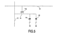
図5はアクティブマトリクス液晶ディスプレイ用の従来型のピクセル構成を示すものである。このディスプレイは行および列の形のピクセルアレイとして配置されている。ピクセルの各行は共通の行導体10を共有しており、ピクセルの各列は共通の列導体12を共有している。各ピクセルは薄膜トランジスタ14と、列導体12および共通電極18の間に直列に配置された液晶セル16とを備えている。トランジスタ14は行導体10に供給される信号によってスイッチオンまたはスイッチオフされる。したがって行導体10は関連するピクセル行の各トランジスタ14のゲート14aに接続される。各ピクセルは付加的にキャパシタ20を備えている。このキャパシタ20は一端22が次の行電極に、または先行する行電極に、またはセパレートキャパシタ電極に接続される。このキャパシタ20は、トランジスタ14がターンオフされた後でも液晶セル16に信号が保持されるように駆動電圧を蓄積する。
FIG. 5 shows a conventional pixel configuration for an active matrix liquid crystal display. The display is arranged as a pixel array in the form of rows and columns. Each row of pixels shares a
液晶セル16を所望の電圧で駆動して、必要とされるグレイレベル(単純には黒または白)を得るために、行導体10上の行アドレスパルスに同期して適当な信号が列導体12に供給される。行アドレスパルスは薄膜トランジスタ14をターンオンさせ、それによって列導体12を介して液晶セル16を所望の電圧に充電し、同様にストレージキャパシタ20を同一電圧に充電する。行アドレスパルスの終わりでトランジスタ14がターンオフされるが、ストレージキャパシタ20は他の行がアドレスされている時に、セル16の電圧を保持する。ストレージキャパシタ20が液晶リーケージの効果を低減し、液晶セルキャパシタンスの電圧依存性によって引き起こされるピクセルキャパシタンスのパーセンテージ変化を低減させる。
In order to drive the
行は、すべての行が1つのフレーム周期内でアドレスされるように順次アドレスされ、次のフレーム周期内でリフレッシュされる。 Rows are sequentially addressed so that all rows are addressed within one frame period and refreshed within the next frame period.
図6に示されているように、ディスプレイピクセルのアレイ34に、行アドレス信号は行駆動回路30によって供給され、ピクセル駆動信号は列アドレス回路32によって供給される。
As shown in FIG. 6, a row address signal is provided by a
アモルファスシリコンまたは多結晶シリコンからなる薄膜デバイスとして構成された薄膜トランジスタを介して駆動するのに十分な電流を供給可能とするためには高ゲート電圧を用いなければならない。特にトランジスタがターンオンされる期間は、ディスプレイがリフレッシュされ行の数によって分割されなければならない全フレーム周期にほぼ等しい。オン状態のためのゲート電圧とオフ状態のためのゲート電圧とは多結晶シリコンディスプレイの場合、オフ状態で必要な小さなリーケージ電流とし、利用できる時間内に液晶セル16を充電または放電するようにオン状態で流れる電流を十分なものとするために、約12ボルトだけ異なる。
In order to be able to supply a current sufficient to drive through a thin film transistor configured as a thin film device made of amorphous silicon or polycrystalline silicon, a high gate voltage must be used. In particular, the period during which the transistor is turned on is approximately equal to the entire frame period during which the display must be refreshed and divided by the number of rows. In the case of a polycrystalline silicon display, the gate voltage for the on state and the gate voltage for the off state are a small leakage current required in the off state, and the
図7は、2つの可能な状態間で回路を駆動するのに必要とされる信号上の電圧レンジが低減される、本発明による第1スイッチ装置を示すものである。アレイ装置内のスイッチング回路の具体例は後で説明する。 FIG. 7 shows a first switching device according to the invention in which the voltage range on the signal required to drive the circuit between two possible states is reduced. A specific example of the switching circuit in the array device will be described later.
図示のごとく、データ電圧ノード40と出力信号ノード43との間にキャパシタCBが接続されている。2つのスイッチングトランジスタ50は逆極性形である。データ電圧が転送スイッチ42によってデータ電圧ノード40に印加されると、入力信号は、ターンオンされるべきTFTに存在するゲート・ソース電圧を最高にする電圧レベルに保持される。これは、n形TFTの入力端に加えられる信号1がその最低電圧レベルにあり、p形TFTの入力端の信号2がその最高電圧レベルにあるべきことを意味する。その時、データ電圧ノード40は転送スイッチ42によってデータソースから絶縁され、データ電圧はキャパシタCBに保持される。出力信号電圧のいかなる変化もデータ電圧ノード40で結合され、それにより、導通しているデバイスのゲート・ソース電圧が維持される。これの利点は上述の分析で用いられた波形例の2つのセットを考慮することによって示すことができる。
As shown, the capacitor C B is connected between a
図8は、図3の波形がブートストラップキャパシタCBを用いる、図7のピクセル装置に適するようにいかに修正されうるかを示すものである。新しい波形「転送データ」が追加されている。この信号が高(ハイ)の時、データ電圧レベルがデータソースからデータ電圧ノード40に転送される。この信号が低(ロー)の時、データ電圧ノード40はデータソースから絶縁される。この機能は図7に示されているTFTスッチを用いて達成されうる。スイッチング回路にキャパシタCBを導入することの効果は、データ電圧ノードに現れる電圧波形を修正することにある。n形デバイスをスイッチオンさせるのに必要なデータ電圧は、信号1の入力端に存在する電圧がその最低レベルにある時、データ電圧がデータソースから転送されることによって極小化することができる。このようにして「転送データ」波形内の第2パルスは「信号1」波形の谷に対応するようにタイミングがとられる。
Figure 8 shows how the waveform of FIG. 3 uses a bootstrap capacitor C B, may be modified how to suit the pixel unit of FIG. A new waveform "transfer data" has been added. When this signal is high, the data voltage level is transferred from the data source to the
2つのトランジスタをスイッチングするのに必要とされるデータ電圧レベルが表3に要約されている。 The data voltage levels required to switch the two transistors are summarized in Table 3.
p形デバイスに対するスイッチング条件は、CBが存在しなかった時は前述の場合から変わっていない。しかしここでn形トランジスタをターンオンさせるのに必要とする高データ電圧レベルは低減している。データ電圧がデータ電圧ノードに転送され、それによってVnonというデータ電圧がn形デバイスをターンオンさせるのに十分である時、信号1は0Vである。信号1入力端に印加される電圧がレベルVDRに変化した時、電圧のこの変化はCBによってデータ電圧ノードで結合される。というのは、今やデータ電圧ノードはデータソースから絶縁されるからである。TFTのゲート電圧はほぼVDH+VDRに上昇し、それが、n形デバイスがそのソースおよびドレーン端子の電圧上昇にもかかわらず導通状態を維持するように保証する。このブートストラッピング効果の重要性は、n形デバイスをスイッチングするのに必要な高レベルデータ電圧がわずか4Vにすぎないことである。これはp形デバイスを非導通状態に維持するのに必要とする高レベル電圧より低く、そのため、この例において用いられる特定の値に対して最低必要な高データ電圧レベルは4.5Vである。実際上、CBのブートストラッピング効果はデータ電圧ノードにおける他のキャパシタンスの存在に影響されるので完全なものではない。このキャパシタンスの存在はソース電圧の変化より小さいトランジスタのゲート電圧に変化を生じさせる。そのため、信号電圧が上昇した時、ゲート・ソース電圧は低減し、トランジスタはその導通度が低下することになる。このことが多少高いデータ電圧の使用を必要とすることになる。それは簡単な分析によって説明することができる。
switching conditions for p-type devices, when the C B not exist has not changed from the previous case. However, the high data voltage level required to turn on the n-type transistor here is reduced.
この例はスイッチング回路にキャパシタCBを導入し、信号電圧が最適レベルにある時、データ電圧をデータ電圧ノードに転送してその後、そのノードを絶縁することによって、必要とするデータ電圧レンジの実質的縮小が達成可能であり、それによりディスプレイの電力消費量を減少させることができる。 This example introduces a capacitor C B to the switching circuit, when the signal voltage is the optimal level, then transfer the data voltage to the data voltage node, by isolating the nodes, real data voltage range that requires Reduction can be achieved, thereby reducing the power consumption of the display.
図9は、図4の波形がブートストラップキャパシタCBを用いた図7のピクセル装置に適合するようにいかに修正されうるかを示すものである。ここでも「転送データ」波形はデータ電圧がデータ電圧ノードに転送されるタイミングを示している。信号1がその最低レベルにあり、信号2がその最高レベルにある時、データ電圧をデータ電圧ノードに転送することによって、p形およびn形TFTをスイッチングするのに必要とする高低データ電圧レベル間の差(電圧レンジ)を減少させることが可能である。先例におけるように、CBの効果は、データ電圧ノードをデータ電圧ソースから絶縁することによって出力電圧の変化をデータ電圧ノードに結合することである。データ電圧が当初、低レベルVDLにあり、信号2がその最低値になった時、出力駆動電圧が同一レベルに低下し、キャパシタCBがその電圧変化をデータ電圧ノードで結合する。これは、p形デバイスを導通状態に維持するように保証する。データ電圧が当初、高レベルVDHにあり、信号1がその最高値に移行した時、出力駆動電圧が同一レベルに上昇し、キャパシタCBがその変化をデータ電圧ノードで結合する。それにより、n形デバイスを導通状態に維持するように保証する。CBを含むスイッチング回路に対する必要データ電圧が表4に要約されている。
Figure 9 shows how the waveform of FIG. 4 can how be modified to conform to the pixel unit of FIG. 7 using a bootstrap capacitor C B. Again, the “transfer data” waveform indicates the timing at which the data voltage is transferred to the data voltage node. When
上述の条件に対して必要とされるデータ電圧振幅は、入力駆動波形をスイッチングした時、n形およびp形TFTが導通状態を維持することを保証する必要性によって決定される。ここでもデータ信号振幅はキャパシタCBの導入によりほぼ4.5Vという値に低減される。 The data voltage amplitude required for the above conditions is determined by the need to ensure that the n-type and p-type TFTs remain conductive when the input drive waveform is switched. Again the data signal amplitude is reduced to a value of approximately 4.5V by the introduction of the capacitor C B.
本発明のこの実施例は、p形またはn形薄膜トランジスタの回路を用いて信号を選択し、またはルート指定し、または多重化する方法を提供するものであることが理解できるであろう。スイッチングトランジスタの出力信号がそのゲートに容量的に結合されるブートストラッピング技術はトランジスタを制御するのに用いられる比較的低データ電圧または制御信号電圧を可能にする。回路を正しく動作させるには信号特性についての多少の知識が必要なものである。というのは、通過する信号電圧がp形およびn形デバイスに対してそれぞれその最高電圧レベル(正極性最大値)または最低電圧レベル(負極性最大値)にある時に、制御データをトランジスタに転送するのが好ましいからである。このアプローチはスイッチを制御するのに用いられる信号の電圧レンジを極小化する。 It will be appreciated that this embodiment of the present invention provides a method for selecting, routing, or multiplexing signals using p-type or n-type thin film transistor circuitry. A bootstrapping technique in which the output signal of a switching transistor is capacitively coupled to its gate allows for a relatively low data voltage or control signal voltage used to control the transistor. Some knowledge of signal characteristics is required to make the circuit operate correctly. This is because the control data is transferred to the transistor when the passing signal voltage is at its highest voltage level (maximum positive polarity) or lowest voltage level (maximum negative polarity) for the p-type and n-type devices, respectively. This is because it is preferable. This approach minimizes the voltage range of the signal used to control the switch.
TFTによりこれを通過する信号電圧の最低レベルがVmin、最高レベルがVmaxであるとすれば、従来型のアプローチおよび本提案のブートストラップ型アプローチを用いたデバイスをスイッチングするのに必要なデータまたは制御電圧レベルはn形デバイスに関して表5に示され、p形デバイスに関して表6に示されている通りである。ここでは、データ電圧ノードの全キャパシタンスに対するブートストラッピングキャパシタCBの比がkBに等しいと仮定されている。 If the minimum level of the signal voltage passing through the TFT is V min and the maximum level is V max , the data required to switch the device using the conventional approach and the proposed bootstrap approach Or the control voltage levels are as shown in Table 5 for n-type devices and as shown in Table 6 for p-type devices. Here, it is assumed that the ratio of the bootstrapping capacitor C B to the total capacitance of the data voltage node is equal to k B.
これらの例はブートストラッピング技術が2つの信号選択機能の1つに適用可能であることを示すものである。しかし、本発明はスイッチングトランジスタの他の構成に対しても適用可能である。 These examples show that bootstrapping techniques can be applied to one of two signal selection functions. However, the present invention can be applied to other configurations of the switching transistor.
図10はワンオブフォー(one−of−four)選択回路の一例を示すものである。4つのスイッチングトランジスタ50のうちの1つをターンオンさせるようして制御信号「データ1」ないし「データ4」が発生される。図10に示されているようにp形およびn形TFTの組合せが用いられうる。しかし同じ形のトランジスタを用いることもできる。
FIG. 10 shows an example of a one-of-four selection circuit. Control signals “
図11は2ビット電圧セレクタの一例を示すものである。これは、デコーディングおよび信号スイッチング機能を提供するために直列接続されたスイッチングトランジスタを使用している。 FIG. 11 shows an example of a 2-bit voltage selector. This uses switching transistors connected in series to provide decoding and signal switching functions.
このスイッチング回路は4つの入力端(「信号0」ないし「信号3」)を持ち、それらのうちの1つが2ビット制御信号D0,D1によって選択される。この回路は2つの層52,54を持っている。第1層52は入力端のそれぞれと2つの中間出力端56,58の一方との間に接続された第1ないし第4スイッチングトランジスタ50a〜50dを備えている。第1層52は2ビットワードの両ビットD0の一方によって制御される。このビットは信号入力端のどの2つが中間出力端にルート指定されるかを決定する。第2層54は中間出力端の信号のうちの1つを出力信号として選択的にルート指定する。第2層54は制御信号の他方のビットD1によって制御される。このようにして図11の回路はワンオブツー(one−of−two)選択回路のカスケード(縦続接続回路)として形成される。
This switching circuit has four inputs (“signal 0” to “signal 3”), one of which is selected by the 2-bit control signals D0 and D1. This circuit has two
本発明の回路は数多くのアプリケーションで用いられうる。アプリケーションは本質的に、「転送データ」信号のタイミングがブートストラップキャパシタの容量性結合の利点を取り込むように選択されるべく、入力信号波形が知られていることを必要とする。本発明はスイッチング電圧レベルを低下させることができ、マルチプレクサ回路でもアレイ型回路構成の範囲内でも使用可能である。 The circuit of the present invention can be used in many applications. The application essentially requires that the input signal waveform be known so that the timing of the “transfer data” signal is selected to take advantage of the capacitive coupling of the bootstrap capacitor. The present invention can reduce the switching voltage level and can be used in both multiplexer circuits and array circuit configurations.
本発明の回路の1つの特別有利な用途はアクティブマトリクスディスプレイ装置、特にピクセル設計に係るディスプレイ装置にある。その場合、この回路は例えば低電力バイナリディスプレイモード用の2つの輝度レベル間の選択を提供することができる。本発明はまた次に述べるように集積型メモリ能力を有するディスプレイに特に適したものである。 One particularly advantageous application of the circuit of the invention is in active matrix display devices, in particular display devices according to pixel design. In that case, the circuit may provide a choice between two luminance levels, for example for a low power binary display mode. The present invention is also particularly suitable for displays having integrated memory capabilities as described below.
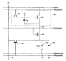
本発明の回路を使用するAMLCD用のピクセル回路の一例が図12に示されている。このピクセルは図5の標準ピクセル回路を含んでおり、図5のものと同一の部品には同一符号が用いられている。これらの部品はピクセルがノーマルアナログドライブモードで動作することを可能にする。これは動作の第1モードと考えられうる。 An example of a pixel circuit for AMLCD using the circuit of the present invention is shown in FIG. This pixel includes the standard pixel circuit of FIG. 5, and the same reference numerals are used for the same components as in FIG. These components allow the pixel to operate in normal analog drive mode. This can be considered a first mode of operation.
このピクセルも図7を参照して説明したスイッチング回路に対応するスイッチング回路60を含んでいる。ここでも図7と同一の部品には同一の参照符号が用いられている。このスイッチング回路60は、すべてのピクセル間で共有される2つの駆動電圧レベル「Vdrive1」および「Vdrive2」のいずれか一方の選択を可能とする。スイッチングトランジスタのゲートにデータ信号を印加するタイミングを制御する転送スイッチ42は、複数のピクセルの複数の行間で共有される「Data_address」(データアドレス)ラインによって制御される。選択された駆動信号はスイッチング回路60の共通出力端62と第1選択スイッチ64によってアドレスされる液晶セル16との間で結合される。なお、第1選択スイッチ64は「Pixel_refresh」(ピクセルリフレッシュ)ラインによって制御される。「Pixel_refresh」の機能は次に説明する。トランジスタ14は第2転送スイッチと見ることができる。これら2つの転送スイッチ(42,14)は、ピクセルの一部(アナログまたはバイナリパート)が駆動信号を液晶セル16に供給するように指令する。
This pixel also includes a switching
このようにしてピクセルを2つの動作モードで動作させることができる。第1のアナログモードでは、ディスプレイ素子が第1転送スイッチ64によってスイッチング回路60から絶縁されるように、Pixel_refresh電極が低レベルに保持される。第2の動作モードでは、ディジタルデータ信号が列12に印加される。正極性のパルスをData_addressラインに印加することによってデータの1ビットが列電極12からデータ電圧ノード40に転送される。これは転送スイッチ42をターンオンさせ、ブートストラッピングキャパシタCBを充電状態にする。
In this way, the pixel can be operated in two modes of operation. In the first analog mode, the Pixel_refresh electrode is held at a low level so that the display element is isolated from the switching
ブートストラッピングキャパシタはディジタルデータをピクセル内に蓄積するキャパシタンスとしても作用することができる。上述のように、このデータ転送は、スイッチングトランジスタ50をスイッチングするのに必要とされるディジタルデータ電圧のレンジを極少化するために、信号Vdrive1がその最低電圧レベルにあり、信号Vdrive2がその最高電圧レベルにある時に行われる(図9を参照して説明したように)。データがデータ電圧ノードに転送された後、スイッチングトランジスタ50のうちの1つが導通状態になり、他のデバイスは非導通状態になる。したがって、2つの信号Vdrive1およびVdrive2のうちの一方がスイッチング回路の出力端62に現れる。
The bootstrapping capacitor can also act as a capacitance that stores digital data in the pixel. As described above, this data transfer is such that signal Vdrive1 is at its lowest voltage level and signal Vdrive2 is at its highest voltage to minimize the range of digital data voltages required to switch switching
この駆動信号は、Pixel_refreshラインに正極性のパルスを印加し、第1転送スイッチ64をターンオンさせることによって、ディスプレイ素子に周期的に、例えば20msごとに印加される。
This drive signal is applied to the display element periodically, for example, every 20 ms by applying a positive pulse to the Pixel_refresh line and turning on the
上述のように、ブートストラッピングキャパシタは集積化メモリ素子として機能することができる。特にこのキャパシタは、2つの信号入力端のどちらが共通の出力端にスイッチングされるかにより異なるレベルに充電される。集積化メモリの能力は、アクティブマトリクスディスプレイ装置の電力消費量の重要な低減策として、ビデオ情報をビデオ信号源からディスプレイ装置のピクセルに転送することに関連して提案されてきた。ディスプレイ装置のピクセルが不特定な時間周期でビデオ情報を記憶することができれば、この電力消費量は低減させることができる。その場合、ピクセルのディスプレイ出力(輝度)状態に変化が必要でない時は、新鮮なビデオ情報を有するピクセルのアドレッシングは一時的に停止することができる。 As described above, the bootstrapping capacitor can function as an integrated memory device. In particular, this capacitor is charged to a different level depending on which of the two signal inputs is switched to the common output. The ability of integrated memory has been proposed in connection with transferring video information from a video signal source to the pixels of the display device as an important reduction in the power consumption of active matrix display devices. This power consumption can be reduced if the pixels of the display device can store video information at unspecified time periods. In that case, the addressing of pixels with fresh video information can be temporarily stopped when no change in the display output (brightness) state of the pixels is necessary.
このようにして、アクティブマトリクスディスプレイ装置のピクセル内へのメモリ組込みは、静止画像ディスプレイが許されるならば、消費電力を減少させることができる。その理由は、画像変化がなく、消費電力が少ない時、つまり外部回路で消費され、駆動にディスプレイピクセルに関連してキャパシタンスが存在する時は、必要なデータがディスプレイピクセルに送出されるだけだからである。本発明のピクセル回路は白黒画像を低減されたアドレッシング電圧レベルによるこの低電力モードで表示することを可能にする。 In this way, incorporating memory into the pixels of an active matrix display device can reduce power consumption if still image displays are allowed. The reason is that when there is no image change and the power consumption is low, that is, when it is consumed by external circuitry and there is a capacitance associated with the display pixel in the drive, only the necessary data is sent to the display pixel. is there. The pixel circuit of the present invention allows black and white images to be displayed in this low power mode with reduced addressing voltage levels.
メモリ素子としてキャパシタが用いられる時、CBに保持されるディジタルデータは周期的にリフレッシュされなければならない。スイッチ64およびCBが1ビットダイナミックメモリセルを効果的に形成するからである。このリフレッシュは、データを外部メモリからディスプレイの列駆動回路および列電極を介して転送することによって達成されうる。代替的に、それは記憶されたデータをトランジスタ14および64を介して列電極上に読み出し、データ信号をバッファするためにトランジスタ50によって形成されるスイッチング回路を用いることによって達成されうる。いずれの場合でも、ブートストラッピング技術によって生ずるディジタルデータ信号の振幅の減少がディスプレイの列に印加されねばならないディジタル信号の振幅を減少させ、このことがまたディスプレイの電力消費量を減少させる。
When the capacitor is used as a memory element, the digital data held in C B must be periodically refreshed.
ディジタルデータをリフレッシュすべき周波数はキャパシタCBの値、および転送トランジスタ42を通って流れるリーケージ電流に依存する。一般的には5Hzないし30Hzの範囲の周波数が適当である。
Frequencies to be refreshed digital data is dependent on the leakage current flowing through the value of the capacitor C B, and the
上記の実施例においては、少なくとも2つの駆動電圧のうちの1つを選択し、それを共通の出力端に供給するスイッチング回路が用いられている。しかし、ブートストラッピング技術は本発明のスイッチング装置を用いてスイッチングされるただ1つの駆動電圧を有するAMLCDピクセル回路に適用することができる。図13はこの目的のために図12に対する修正を示すものである。図13において、図12と同じ部品には同じ参照符号が用いられている。 In the above embodiment, a switching circuit is used that selects one of at least two drive voltages and supplies it to a common output terminal. However, bootstrapping techniques can be applied to AMLCD pixel circuits having only one drive voltage that is switched using the switching device of the present invention. FIG. 13 shows a modification to FIG. 12 for this purpose. 13, the same reference numerals are used for the same components as in FIG.
図13のピクセル回路は図12の回路と同様の態様で動作することができる。しかし、それはブートストラップキャパシタCBに記憶されたデータによって制御されるただ1つのスイッチングトランジスタ50しか備えていない。列データ電圧が高であって、転送スイッチ42によってスイッチングトランジスタ50にルート指定されると、スイッチングトランジスタ50がターンオンされる。Pixel_refreshラインが高にされると、ピクセルは転送スイッチ64を介してVdrive1のレベルに充電される。
The pixel circuit of FIG. 13 can operate in a manner similar to the circuit of FIG. However, it has only one
列データ電圧が低である時、スイッチングトランジスタ50がターンオフされ、また、Pixel_refreshラインが高にされると、ピクセル電圧は不変に維持される。ピクセルを暗状態または明状態にスイッチングするために、必要とされる第2ピクセル駆動電圧レベルはピクセルキャパシタンスの予充電を用いることによってピクセルに印加されうる。ピクセルはディスプレイの列に予充電電圧(例えば図12におけるピクセル回路例のVdrive2に類似)を印加することによって予充電され、トランジスタスイッチ64の前にピクセルアドレストランジスタ14を一時的にターオンさせる。この方式において、もし列データ電圧が高であれば、ピクセル電極に生ずる電圧はVdrive1であり、もし列データ電圧が低であれば、ピクセル電極に生ずる電圧は予充電電圧(Vdrive2)である。
When the column data voltage is low, when the switching
このようにしてピクセルがアドレスされる直前にピクセルにVdrive2の予充電が行われる。もし列データ電圧が高であれば、それは無効にされ、それに対して列データ電圧が低であれば、ピクセルにVdrive2が残る。ピクセルアドレスモード中、トランジスタ14はターオフされる。
In this way, Vdrive2 is precharged to the pixel immediately before the pixel is addressed. If the column data voltage is high, it is disabled, while if the column data voltage is low, Vdrive2 remains in the pixel. During pixel address mode,
図13の回路では、トランジスタ50はディジタルスイッチング回路のスイッチングトランジスタの1つとして作用し、トランジスタ14は他のトランジスタとして作用する。それらは中間の共通出力端を共有することはないが、各入力端と効率的に共通出力端となるLCセル16との間に効率的に接続される。それに応じて特許請求の範囲は適宜解釈されなければならない。
In the circuit of FIG. 13,
この場合、データ信号印加のタイミングは、Data_addressパルスを図8の信号1に対応するVdrive1信号の最低電圧でタイミングをとることによって、列データの必要とする電圧レンジをさらに減少させる。同様に、ピクセルアドレストランジスタ14を介してピクセルに転送するために列に印加される予充電電圧は図8の信号2に対応する。
In this case, the timing of applying the data signal further reduces the voltage range required for the column data by timing the Data_address pulse at the lowest voltage of the Vdrive1 signal corresponding to the
上述の例においてブートストラップキャパシタは各スイッチングトランジスタのゲートと共通の出力端との間に接続される。しかし、入力信号を選択するスイッチングトランジスタの出力端が共通の出力ノードに直接には接続されない時は、いくつかの状況がありうる。図14のピクセル回路はD/Aコンバータを含んでいる。これは、ピクセルがトランジスタT1を用いてある一定の電圧に予充電されるが、Vdrive1からの電圧ステップを、コンバータキャパシタCCを介してピクセル上で結合することによってピクセル電圧を変化させることができる、図13のピクセル回路に類似する態様で動作する。 In the above example, the bootstrap capacitor is connected between the gate of each switching transistor and the common output terminal. However, there may be several situations when the output ends of the switching transistors that select the input signal are not directly connected to the common output node. The pixel circuit of FIG. 14 includes a D / A converter. This pixel but are precharged to a predetermined voltage that is using the transistor T1, it can be a voltage step from Vdrive1, changing the pixel voltage by binding on the pixel through the converter capacitor C C Operates in a manner similar to the pixel circuit of FIG.
ピクセル上で結合される電圧の大きさはキャパシタCBのデータ電圧に対応する。注意すべきことは、スイッチングトランジスタの出力端が共通の出力ノードに結合されるのであるが、それは直列接続された付加的なキャパシタを介してであることである。これはディジタルワードから「データ」ライン上でのD/A変換を提供する。 The magnitude of the voltage coupled on pixels corresponding to the data voltage of the capacitor C B. It should be noted that the output terminals of the switching transistors are coupled to a common output node, but through an additional capacitor connected in series. This provides D / A conversion on the “data” line from the digital word.
本発明の根本的な技術は、ディジタル制御またはデータ信号の状態に基づいて信号をルート指定し、または信号を選択する回路を作り出すために、p形トランジスタまたはn形トランジスタの組合せ、あるいは両者の組合せを用いることが望ましい状況の下に非常に広く適用することができる。上に要約したように、この技術は、ピクセル内に集積化したダイナミックメモリがその輝度を制御するために用いられるディスプレイに使用するのに特に有意義なものである。 The underlying technique of the present invention is a combination of p-type transistors or n-type transistors, or a combination of both, to create a circuit that routes or selects signals based on the state of a digital control or data signal. Can be applied very widely under circumstances where it is desirable to use. As summarized above, this technique is particularly meaningful for use in displays in which dynamic memory integrated in pixels is used to control its brightness.
用語「行」および「列」は明細書および特許請求の範囲において多少恣意的に用いられている。これらの用語は、共通接続部を共有する素子の直交ラインによる素子のアレイが存在することを明瞭にすることを意図するものである。行は通常、ディスプレイの左右に横方向に走るものと考えられ、列は上から下に縦方向に走るものと考えられる。 The terms “row” and “column” are used somewhat arbitrarily in the specification and claims. These terms are intended to clarify that there is an array of elements with orthogonal lines of elements sharing a common connection. Rows are usually considered to run horizontally to the left and right of the display, and columns are considered to run vertically from top to bottom.
本発明の他の特徴は当業者には明らかなことであろう。 Other features of the invention will be apparent to those skilled in the art.
Claims (21)
アナログピクセルデータライン(12)と前記ピクセルの液晶セル(16)との間に設けられた第2選択スイッチ(14)と、
をさらに備えている、請求項12に記載の装置。 A first selection switch (64) provided between the common output terminal (62) of the switching circuit (60) and the liquid crystal cell of the pixel (16);
A second selection switch (14) provided between the analog pixel data line (12) and the liquid crystal cell (16) of the pixel;
The apparatus of claim 12, further comprising:
アナログピクセルデータライン(12)と前記ピクセルの液晶セル(16)との間に設けられた第2選択スイッチ(14)と、
をさらに備えている請求項12に記載の装置。 A first selection switch (64) provided between at least one output terminal of the switching circuit (50) and a liquid crystal cell of the pixel;
A second selection switch (14) provided between the analog pixel data line (12) and the liquid crystal cell (16) of the pixel;
The apparatus of claim 12, further comprising:
少なくとも2つの入力端(信号1〜信号4)のそれぞれと前記ピクセル素子(16)との間に接続された少なくとも第1および第2スイッチングトランジスタ(50)のゲートにデータ信号を印加して、前記第1および第2スイッチングトランジスタ(50)のうちの選択された一方をターンオンし、前記第1および第2スイッチングトランジスタ(50)のうちの他方をターンオフし、それによって前記各入力端を前記ピクセル素子(16)にルート指定するステップを備え、その場合、
前記データ信号を印加するタイミングが前記2つの入力端のうちの少なくとも一方の信号に応じて選択され、
少なくとも1つのスイッチングトランジスタ(50)のゲートと前記スイッチングトランジスタの出力端との間に容量性結合部(CB)が設けられ、
前記容量性結合部がスイッチングトランジスタをターンオンおよびターンオフするのに必要なデータ信号に必要とされる電圧変化幅を減少させるように前記タイミングが制御される、
ピクセルのアレイを備えた装置のピクセル内のピクセル素子に少なくとも2つの入力端の一方をルート指定する方法。 In a method of routing one of at least two inputs to a pixel element in a pixel of a device comprising an array of pixels,
Applying a data signal to the gates of at least first and second switching transistors (50) connected between each of at least two input terminals (signal 1 to signal 4) and the pixel element (16); A selected one of the first and second switching transistors (50) is turned on and the other of the first and second switching transistors (50) is turned off, whereby each input terminal is connected to the pixel element. (16) comprises the step of routing, in which case
The timing for applying the data signal is selected according to the signal of at least one of the two input terminals,
A capacitive coupling (C B ) is provided between the gate of at least one switching transistor (50) and the output end of the switching transistor;
The timing is controlled to reduce the voltage variation required for the data signal required for the capacitive coupling to turn on and off the switching transistor;
A method of routing one of at least two inputs to a pixel element in a pixel of a device comprising an array of pixels.
第2モードにおいて、2つのピクセル駆動信号のうちの一方を前記ディスプレイの各ピクセルにルート指定する
ステップを備え、前記ルート指定は前記第2モードにおいて各ピクセルに対して請求項20に記載の方法を用いる、
液晶ディスプレイを駆動する方法。 In a first mode, switching an analog pixel drive signal to each pixel of the display;
21. The method of claim 20, comprising routing one of two pixel drive signals to each pixel of the display in a second mode, wherein the routing is for each pixel in the second mode. Use
A method of driving a liquid crystal display.
Applications Claiming Priority (2)
| Application Number | Priority Date | Filing Date | Title |
|---|---|---|---|
| GBGB0217709.5A GB0217709D0 (en) | 2002-07-31 | 2002-07-31 | Array device with switching circuits |
| PCT/IB2003/003220 WO2004013836A1 (en) | 2002-07-31 | 2003-07-16 | Array device with switching circuits with bootstrap capacitors |
Publications (2)
| Publication Number | Publication Date |
|---|---|
| JP2005534971A true JP2005534971A (en) | 2005-11-17 |
| JP2005534971A5 JP2005534971A5 (en) | 2006-07-06 |
Family
ID=9941431
Family Applications (1)
| Application Number | Title | Priority Date | Filing Date |
|---|---|---|---|
| JP2004525666A Withdrawn JP2005534971A (en) | 2002-07-31 | 2003-07-16 | Array device with switching circuit having bootslap capacitor |
Country Status (9)
| Country | Link |
|---|---|
| US (1) | US20050236650A1 (en) |
| EP (1) | EP1527437A1 (en) |
| JP (1) | JP2005534971A (en) |
| KR (1) | KR20050027136A (en) |
| CN (1) | CN1672187A (en) |
| AU (1) | AU2003247066A1 (en) |
| GB (1) | GB0217709D0 (en) |
| TW (1) | TW200408864A (en) |
| WO (1) | WO2004013836A1 (en) |
Cited By (5)
| Publication number | Priority date | Publication date | Assignee | Title |
|---|---|---|---|---|
| JP2010160376A (en) * | 2009-01-09 | 2010-07-22 | Toppoly Optoelectronics Corp | Active matrix type display device and electronic apparatus with the same |
| JP2011186094A (en) * | 2010-03-08 | 2011-09-22 | Chi Mei Electronics Corp | Active matrix type display device and electronic apparatus having the same |
| WO2012056804A1 (en) * | 2010-10-26 | 2012-05-03 | シャープ株式会社 | Display device |
| WO2012081530A1 (en) * | 2010-12-17 | 2012-06-21 | シャープ株式会社 | Liquid crystal display device and method for driving same |
| JP2017139048A (en) * | 2008-11-14 | 2017-08-10 | 株式会社半導体エネルギー研究所 | Shift register |
Families Citing this family (12)
| Publication number | Priority date | Publication date | Assignee | Title |
|---|---|---|---|---|
| KR101002324B1 (en) * | 2003-12-22 | 2010-12-17 | 엘지디스플레이 주식회사 | Liquid Crystal Display Device and Driving Method Thereof |
| KR20060025785A (en) * | 2004-09-17 | 2006-03-22 | 삼성전자주식회사 | Liquid crystal display |
| DE102006056089A1 (en) | 2006-11-28 | 2008-05-29 | Festo Ag & Co. | valve means |
| CN101833186B (en) * | 2009-03-10 | 2011-12-28 | 立景光电股份有限公司 | Pixel circuit of display device |
| US8363380B2 (en) | 2009-05-28 | 2013-01-29 | Qualcomm Incorporated | MEMS varactors |
| US8866719B2 (en) * | 2009-09-16 | 2014-10-21 | Sharp Kabushiki Kaisha | Memory device and liquid crystal display device equipped with memory device |
| US20110148837A1 (en) * | 2009-12-18 | 2011-06-23 | Qualcomm Mems Technologies, Inc. | Charge control techniques for selectively activating an array of devices |
| US8218228B2 (en) * | 2009-12-18 | 2012-07-10 | Qualcomm Mems Technologies, Inc. | Two-terminal variable capacitance MEMS device |
| US8773193B2 (en) * | 2012-07-13 | 2014-07-08 | Wispry, Inc. | Methods, devices, and systems for switched capacitor array control |
| CN107578751B (en) * | 2017-09-20 | 2020-06-26 | 京东方科技集团股份有限公司 | Data voltage storage circuit, driving method, liquid crystal display panel and display device |
| CN111554237B (en) | 2020-06-10 | 2021-10-15 | 京东方科技集团股份有限公司 | Multiplexing circuit, method, multiplexing module and display device |
| CN112904606B (en) * | 2020-12-28 | 2022-03-04 | 山东蓝贝思特教装集团股份有限公司 | Bistable liquid crystal writing device with quick electric driving display function and method |
Family Cites Families (8)
| Publication number | Priority date | Publication date | Assignee | Title |
|---|---|---|---|---|
| US5105288A (en) * | 1989-10-18 | 1992-04-14 | Matsushita Electronics Corporation | Liquid crystal display apparatus with the application of black level signal for suppressing light leakage |
| US6072454A (en) * | 1996-03-01 | 2000-06-06 | Kabushiki Kaisha Toshiba | Liquid crystal display device |
| CN1198172C (en) * | 1999-12-03 | 2005-04-20 | 三菱电机株式会社 | Liquid crystal display |
| JP3705123B2 (en) * | 2000-12-05 | 2005-10-12 | セイコーエプソン株式会社 | Electro-optical device, gradation display method, and electronic apparatus |
| JP4552069B2 (en) * | 2001-01-04 | 2010-09-29 | 株式会社日立製作所 | Image display device and driving method thereof |
| JP3618687B2 (en) * | 2001-01-10 | 2005-02-09 | シャープ株式会社 | Display device |
| TW554558B (en) * | 2001-07-16 | 2003-09-21 | Semiconductor Energy Lab | Light emitting device |
| KR100803163B1 (en) * | 2001-09-03 | 2008-02-14 | 삼성전자주식회사 | Liquid crystal display apparatus |
-
2002
- 2002-07-31 GB GBGB0217709.5A patent/GB0217709D0/en not_active Ceased
-
2003
- 2003-07-16 AU AU2003247066A patent/AU2003247066A1/en not_active Abandoned
- 2003-07-16 JP JP2004525666A patent/JP2005534971A/en not_active Withdrawn
- 2003-07-16 CN CNA038181274A patent/CN1672187A/en active Pending
- 2003-07-16 KR KR1020057001601A patent/KR20050027136A/en not_active Application Discontinuation
- 2003-07-16 WO PCT/IB2003/003220 patent/WO2004013836A1/en active Application Filing
- 2003-07-16 US US10/522,847 patent/US20050236650A1/en not_active Abandoned
- 2003-07-16 EP EP03766541A patent/EP1527437A1/en not_active Withdrawn
- 2003-07-28 TW TW092120519A patent/TW200408864A/en unknown
Cited By (9)
| Publication number | Priority date | Publication date | Assignee | Title |
|---|---|---|---|---|
| JP2017139048A (en) * | 2008-11-14 | 2017-08-10 | 株式会社半導体エネルギー研究所 | Shift register |
| US10416517B2 (en) | 2008-11-14 | 2019-09-17 | Semiconductor Energy Laboratory Co., Ltd. | Liquid crystal display device |
| US10901283B2 (en) | 2008-11-14 | 2021-01-26 | Semiconductor Energy Laboratory Co., Ltd. | Liquid crystal display device |
| US11604391B2 (en) | 2008-11-14 | 2023-03-14 | Semiconductor Energy Laboratory Co., Ltd. | Liquid crystal display device |
| JP2010160376A (en) * | 2009-01-09 | 2010-07-22 | Toppoly Optoelectronics Corp | Active matrix type display device and electronic apparatus with the same |
| JP2011186094A (en) * | 2010-03-08 | 2011-09-22 | Chi Mei Electronics Corp | Active matrix type display device and electronic apparatus having the same |
| WO2012056804A1 (en) * | 2010-10-26 | 2012-05-03 | シャープ株式会社 | Display device |
| US8767136B2 (en) | 2010-10-26 | 2014-07-01 | Sharp Kabushiki Kaisha | Display device |
| WO2012081530A1 (en) * | 2010-12-17 | 2012-06-21 | シャープ株式会社 | Liquid crystal display device and method for driving same |
Also Published As
| Publication number | Publication date |
|---|---|
| KR20050027136A (en) | 2005-03-17 |
| CN1672187A (en) | 2005-09-21 |
| AU2003247066A1 (en) | 2004-02-23 |
| EP1527437A1 (en) | 2005-05-04 |
| GB0217709D0 (en) | 2002-09-11 |
| US20050236650A1 (en) | 2005-10-27 |
| WO2004013836A1 (en) | 2004-02-12 |
| TW200408864A (en) | 2004-06-01 |
Similar Documents
| Publication | Publication Date | Title |
|---|---|---|
| KR100532653B1 (en) | Liquid crystal display apparatus having pixels with low leakage current | |
| KR100347654B1 (en) | Power-saving circutt and method for driving liquid crystal display | |
| EP0750288B1 (en) | Liquid crystal display | |
| JP2005534971A (en) | Array device with switching circuit having bootslap capacitor | |
| US8775842B2 (en) | Memory device, display device equipped with memory device, drive method for memory device, and drive method for display device | |
| JP5788587B2 (en) | Pixel circuit, display circuit and display device suitable for active storage pixel inversion, and driving method of pixel circuit | |
| US11132930B2 (en) | Display device, source drive circuit and display system | |
| US8866719B2 (en) | Memory device and liquid crystal display device equipped with memory device | |
| US7102612B2 (en) | Power-saving circuits and methods for driving active matrix display elements | |
| US6756961B2 (en) | Active matrix display device | |
| US20120200549A1 (en) | Display Device And Drive Method For Display Device | |
| US8791895B2 (en) | Liquid crystal display device and drive method therefor | |
| EP1552498A1 (en) | Active matrix display | |
| US20120176393A1 (en) | Memory device, display device equipped with memory device, drive method for memory device, and drive method for display device | |
| JP2003228345A (en) | Liquid crystal display device | |
| US6731262B2 (en) | Active matrix display device | |
| US11508302B2 (en) | Method for driving display panel and related driver circuit | |
| US7245296B2 (en) | Active matrix display device | |
| CN111710280B (en) | Display panel, driving method thereof and electronic equipment | |
| US20230124102A1 (en) | Driving method and driving device for display panel and display device | |
| JP2003140109A (en) | Liquid crystal display device |
Legal Events
| Date | Code | Title | Description |
|---|---|---|---|
| A521 | Written amendment |
Free format text: JAPANESE INTERMEDIATE CODE: A523 Effective date: 20060518 |
|
| A621 | Written request for application examination |
Free format text: JAPANESE INTERMEDIATE CODE: A621 Effective date: 20060718 |
|
| RD02 | Notification of acceptance of power of attorney |
Free format text: JAPANESE INTERMEDIATE CODE: A7422 Effective date: 20070420 |
|
| A761 | Written withdrawal of application |
Free format text: JAPANESE INTERMEDIATE CODE: A761 Effective date: 20081029 |