JP2005532902A - Apparatus and method for thermally controlling and processing micro-electronic product workpieces - Google Patents
Apparatus and method for thermally controlling and processing micro-electronic product workpieces Download PDFInfo
- Publication number
- JP2005532902A JP2005532902A JP2004521884A JP2004521884A JP2005532902A JP 2005532902 A JP2005532902 A JP 2005532902A JP 2004521884 A JP2004521884 A JP 2004521884A JP 2004521884 A JP2004521884 A JP 2004521884A JP 2005532902 A JP2005532902 A JP 2005532902A
- Authority
- JP
- Japan
- Prior art keywords
- container
- processing
- processing liquid
- disposed
- heat transfer
- Prior art date
- Legal status (The legal status is an assumption and is not a legal conclusion. Google has not performed a legal analysis and makes no representation as to the accuracy of the status listed.)
- Pending
Links
Images


Classifications
-
- H—ELECTRICITY
- H01—ELECTRIC ELEMENTS
- H01L—SEMICONDUCTOR DEVICES NOT COVERED BY CLASS H10
- H01L21/00—Processes or apparatus adapted for the manufacture or treatment of semiconductor or solid state devices or of parts thereof
- H01L21/67—Apparatus specially adapted for handling semiconductor or electric solid state devices during manufacture or treatment thereof; Apparatus specially adapted for handling wafers during manufacture or treatment of semiconductor or electric solid state devices or components ; Apparatus not specifically provided for elsewhere
- H01L21/67005—Apparatus not specifically provided for elsewhere
- H01L21/67011—Apparatus for manufacture or treatment
- H01L21/67155—Apparatus for manufacturing or treating in a plurality of work-stations
- H01L21/67207—Apparatus for manufacturing or treating in a plurality of work-stations comprising a chamber adapted to a particular process
- H01L21/6723—Apparatus for manufacturing or treating in a plurality of work-stations comprising a chamber adapted to a particular process comprising at least one plating chamber
-
- C—CHEMISTRY; METALLURGY
- C23—COATING METALLIC MATERIAL; COATING MATERIAL WITH METALLIC MATERIAL; CHEMICAL SURFACE TREATMENT; DIFFUSION TREATMENT OF METALLIC MATERIAL; COATING BY VACUUM EVAPORATION, BY SPUTTERING, BY ION IMPLANTATION OR BY CHEMICAL VAPOUR DEPOSITION, IN GENERAL; INHIBITING CORROSION OF METALLIC MATERIAL OR INCRUSTATION IN GENERAL
- C23C—COATING METALLIC MATERIAL; COATING MATERIAL WITH METALLIC MATERIAL; SURFACE TREATMENT OF METALLIC MATERIAL BY DIFFUSION INTO THE SURFACE, BY CHEMICAL CONVERSION OR SUBSTITUTION; COATING BY VACUUM EVAPORATION, BY SPUTTERING, BY ION IMPLANTATION OR BY CHEMICAL VAPOUR DEPOSITION, IN GENERAL
- C23C18/00—Chemical coating by decomposition of either liquid compounds or solutions of the coating forming compounds, without leaving reaction products of surface material in the coating; Contact plating
- C23C18/16—Chemical coating by decomposition of either liquid compounds or solutions of the coating forming compounds, without leaving reaction products of surface material in the coating; Contact plating by reduction or substitution, e.g. electroless plating
- C23C18/1601—Process or apparatus
- C23C18/1633—Process of electroless plating
- C23C18/1675—Process conditions
- C23C18/1676—Heating of the solution
-
- H—ELECTRICITY
- H01—ELECTRIC ELEMENTS
- H01L—SEMICONDUCTOR DEVICES NOT COVERED BY CLASS H10
- H01L21/00—Processes or apparatus adapted for the manufacture or treatment of semiconductor or solid state devices or of parts thereof
- H01L21/67—Apparatus specially adapted for handling semiconductor or electric solid state devices during manufacture or treatment thereof; Apparatus specially adapted for handling wafers during manufacture or treatment of semiconductor or electric solid state devices or components ; Apparatus not specifically provided for elsewhere
- H01L21/67005—Apparatus not specifically provided for elsewhere
- H01L21/67011—Apparatus for manufacture or treatment
- H01L21/67098—Apparatus for thermal treatment
- H01L21/67109—Apparatus for thermal treatment mainly by convection
-
- Y—GENERAL TAGGING OF NEW TECHNOLOGICAL DEVELOPMENTS; GENERAL TAGGING OF CROSS-SECTIONAL TECHNOLOGIES SPANNING OVER SEVERAL SECTIONS OF THE IPC; TECHNICAL SUBJECTS COVERED BY FORMER USPC CROSS-REFERENCE ART COLLECTIONS [XRACs] AND DIGESTS
- Y10—TECHNICAL SUBJECTS COVERED BY FORMER USPC
- Y10T—TECHNICAL SUBJECTS COVERED BY FORMER US CLASSIFICATION
- Y10T137/00—Fluid handling
- Y10T137/0318—Processes
Abstract
液体を用いて、超小型電子品加工片を熱的に制御して処理する装置及び方法である。本発明の実施形態による装置は、無電解処理液のような処理液を支持するように構成された処理容器を含む。この容器は、内部の処理液との間で熱を伝達する熱透過型壁を有する。処理容器から溢れ出る処理液を受けるリザーバのような熱伝達装置が、処理容器内の処理液との間で熱を伝達する。熱伝達装置はまた、熱伝達用流体を運ぶ導管或いは電気抵抗加熱器のような、内部又は外部の熱源との間で熱を伝達することもできる。超小型電子品加工片と処理液との間の相互作用は、該超小型電子品加工片の回転速度、及び/又は該超小型電子品加工片を処理液に導入する及び/又は該処理液から引き出す方法を制御することによって、さらに制御することができる。An apparatus and a method for thermally controlling and processing a micro-electronic work piece using a liquid. An apparatus according to an embodiment of the present invention includes a processing vessel configured to support a processing solution such as an electroless processing solution. This container has a heat transmission type wall that transfers heat to and from the processing liquid inside. A heat transfer device such as a reservoir that receives the processing liquid overflowing from the processing container transfers heat to and from the processing liquid in the processing container. The heat transfer device can also transfer heat to or from an internal or external heat source, such as a conduit carrying a heat transfer fluid or an electrical resistance heater. The interaction between the microelectronic product workpiece and the processing liquid may be caused by the rotational speed of the microelectronic product workpiece and / or introducing the microelectronic product workpiece into the processing liquid and / or the processing liquid. Further control can be achieved by controlling the method of withdrawal from.
Description
本発明は、一般に、無電解析出プロセスの温度を制御する方法及び装置のような、超小型電子品加工片を熱的に制御して処理する装置及び方法に向けられる。 The present invention is generally directed to an apparatus and method for thermally controlling and processing microelectronic workpieces, such as a method and apparatus for controlling the temperature of an electroless deposition process.
半導体デバイス及び電界放出ディスプレイのような超小型電子デバイスは、一般に、幾つかの異なる型の機械(「ツール」)を用いて、超小型電子品加工片上及び/又は該超小型電子品加工片内に製造される。多くのこうした加工機は、加工片上で1つ又はそれ以上の手順を行う単一の処理ステーションを有する。他の加工機は、個々の加工片上又はバッチ単位の加工片上で一連の異なる手順を行う複数の処理ステーションを有する。典型的な製造プロセスにおいて、析出段階中に、1つ又はそれ以上の導電性材料層が加工片上に形成される。次に、加工片は、一般的に、エッチング及び/又は研磨手順(すなわち、平坦化)にかけられ、析出された導電層の一部を取り除き、電気的に隔離された接点及び/又は導電線を形成する。 Microelectronic devices, such as semiconductor devices and field emission displays, generally use several different types of machines (“tools”) on and / or within the microelectronic workpiece. To be manufactured. Many such processing machines have a single processing station that performs one or more procedures on the workpiece. Other processing machines have multiple processing stations that perform a series of different procedures on individual workpieces or batchwise workpieces. In a typical manufacturing process, one or more conductive material layers are formed on a workpiece during the deposition stage. The workpiece is then typically subjected to an etching and / or polishing procedure (ie, planarization) to remove a portion of the deposited conductive layer and remove electrically isolated contacts and / or conductive lines. Form.
加工片上に金属又は他の材料をめっきするめっき用ツールは、ますます加工機の有用な種類になっている。電気めっき及び無電解めっき技術を用いて、ニッケル、銅、はんだ、パーマロイ、金、銀、プラチナその他の金属を加工片の上に付着させ、ブランケット層又はパターン層を形成することができる。典型的な金属めっきプロセスは、化学気相成長法(CVD)、物理的気相成長法(PVD)、又は他の適切な方法を用いて、加工片の表面上に種層を析出させることを含む。種層を形成した後、適切な電気めっき又は無電解処理技術によって、金属のブランケット層又はパターン層を加工片上に析出させることができる。いずれのプロセスにおいても、次に、加工片を別の加工機に移す前に、次の手順において、該加工片を洗浄し、エッチングし、及び/又はアニールすることができる。 Plating tools that plate metal or other materials on a workpiece are increasingly becoming a useful type of processing machine. Using electroplating and electroless plating techniques, nickel, copper, solder, permalloy, gold, silver, platinum or other metals can be deposited on the work piece to form a blanket layer or pattern layer. A typical metal plating process involves depositing a seed layer on the surface of a workpiece using chemical vapor deposition (CVD), physical vapor deposition (PVD), or other suitable method. Including. After forming the seed layer, a metal blanket layer or pattern layer can be deposited on the workpiece by suitable electroplating or electroless processing techniques. In either process, the workpiece can then be cleaned, etched, and / or annealed in the following procedure before the workpiece is transferred to another machine.
幾つかの従来の無電解処理技術において、導電性材料を超小型電子品加工片上にめっきするために用いられる流体が、加熱される。例えば、コバルト、ニッケル、タングステンを有するそれらの合金は、一般に、加熱された無電解溶液を用いて、超小型電子品加工片上にめっきされる。無電解溶液の加熱に伴う1つの欠点は、処理温度と、超小型電子品加工片と無電解液体との間の境界面における流れの均一性とを適切に制御することが困難な点である。このことは、超小型電子品加工片の表面に生じる化学めっき反応、及び多数の超小型電子品加工片が処理される際の均一性に悪影響を与えることがある。 In some conventional electroless processing techniques, the fluid used to plate the conductive material onto the microelectronic workpiece is heated. For example, those alloys comprising cobalt, nickel, tungsten are typically plated onto microelectronic workpieces using a heated electroless solution. One drawback associated with heating the electroless solution is that it is difficult to properly control the processing temperature and flow uniformity at the interface between the microelectronic workpiece and the electroless liquid. . This may adversely affect the chemical plating reaction that occurs on the surface of the microelectronic product workpiece and the uniformity when multiple microelectronic workpieces are processed.
本発明は、超小型電子品加工片が処理される温度を制御する装置及び方法に向けられる。本発明の幾つかの実施形態の1つの態様は、処理中に超小型電子品加工片に接触する(無電解処理液のような)処理液の温度を制御する段階を含む。例えば、1つの特定の態様において、処理液は、超小型電子品加工片と接触させるように処理容器内に配置される。処理容器は、薄い及び/又は熱透過型の壁を有し、該処理容器との間で熱を容易に伝達することを可能にする。熱伝達装置が、処理容器の外側に配置され、熱透過型壁を通して該処理容器との間で熱を伝達する。本発明の更に別の態様において、熱伝達装置は、処理容器から溢れ出る処理液を受けるために、該処理容器から外側に配置された第2の容器を含む。第2の容器は、処理容器の熱透過型壁と熱的に連通している処理液を支持する。本発明の更に別の態様において、電気抵抗加熱器又は熱伝達用流体の源に連結されたコイルのような熱交換器が、第2の容器内に配置される。したがって、温度感性プロセスをより効果的に実行するために、処理容器内の温度を正確に制御することができる。 The present invention is directed to an apparatus and method for controlling the temperature at which a microelectronic workpiece is processed. One aspect of some embodiments of the present invention includes controlling the temperature of a processing solution (such as an electroless processing solution) that contacts a microelectronic workpiece during processing. For example, in one particular embodiment, the processing liquid is placed in the processing vessel so as to contact the microelectronic workpiece. The processing vessel has thin and / or heat transmissive walls, allowing easy transfer of heat to and from the processing vessel. A heat transfer device is disposed outside the processing vessel and transfers heat to and from the processing vessel through a heat transmissive wall. In yet another aspect of the present invention, the heat transfer device includes a second container disposed outside the processing container for receiving the processing liquid overflowing from the processing container. The second container supports a processing liquid that is in thermal communication with the heat-permeable wall of the processing container. In yet another aspect of the present invention, a heat exchanger, such as a coil connected to an electrical resistance heater or a source of heat transfer fluid, is disposed in the second vessel. Therefore, the temperature in the processing vessel can be accurately controlled in order to perform the temperature sensitive process more effectively.
本発明の別の態様において、処理液は、一次出口開口部と少なくとも1つの二次出口開口部とを有する拡散装置を通して、処理容器内に進む。一次出口開口部は、少なくとも1つの二次出口開口部より大きいので、例えば、拡散装置を通過する総流量の約20%から約50%までが、該一次出口開口部を通過する。 In another aspect of the invention, the processing liquid is advanced into the processing vessel through a diffusion device having a primary outlet opening and at least one secondary outlet opening. Since the primary outlet opening is larger than the at least one secondary outlet opening, for example, from about 20% to about 50% of the total flow rate through the diffuser passes through the primary outlet opening.
本発明の他の態様による方法が、処理液と超小型電子品加工片との間の相互作用の他の特性を制御することに向けられる。本発明の1つの態様において、処理中に超小型電子品加工片に付加される材料の分布は、処理液に接触しながら超小型電子品加工片が回転する速度を制御することによって制御される。本発明の別の態様によると、超小型電子品加工片の表面における温度分布は、該超小型電子品加工片が回転する速度を制御することによって、処理中に制御される。 The method according to another aspect of the invention is directed to controlling other properties of the interaction between the processing liquid and the microelectronic workpiece. In one aspect of the invention, the distribution of the material added to the microelectronic workpiece during processing is controlled by controlling the speed at which the microelectronic workpiece is rotated while in contact with the processing liquid. . According to another aspect of the invention, the temperature distribution at the surface of the microelectronic workpiece is controlled during processing by controlling the speed at which the microelectronic workpiece is rotated.
本発明の更に別の態様による方法において、処理前及び/又は処理語に、熱が、超小型電子品加工片と処理液との間で伝達される。例えば、処理液を加熱する際には、(該処理液に接触させる前に)該処理液に近接し且つ該処理液から離間した状態で超小型電子品加工片を配置し、該超小型電子品加工片を予熱する。処理後に超小型電子品加工片を冷却する速度は、処理が完了した後に、該超小型電子品加工片を処理液に近接し且つ該処理液から離間した状態で位置決めすることによって制御される。 In a method according to yet another aspect of the present invention, heat is transferred between the microelectronic workpiece and the processing liquid prior to processing and / or processing words. For example, when the processing liquid is heated, the microelectronic product processed piece is disposed in a state of being close to the processing liquid and separated from the processing liquid (before being brought into contact with the processing liquid). Preheat the workpiece. The rate at which the microelectronic product workpiece is cooled after processing is controlled by positioning the microelectronic product workpiece in proximity to and away from the processing liquid after processing is complete.
次の説明は、超小型電子品加工片を処理するための処理ステーション、一体型ツール、及び関連した方法の幾つかの実施形態の詳細及び特徴を開示するものである。「超小型電子品加工片」という用語は、その上及び/又はその中で超小型電子回路又はコンポーネント、データ記憶素子又は層、及び/又は超小型機械素子が製造される基板から形成された加工片を含むものとして、全体を通して用いられる。基板の特徴は、トレンチ、バイアス、ライン、及び孔のようなサブミクロンの特徴(例えば、0.1μから0.75μまでの範囲のサブミクロン寸法を有する)を含むことができる。以下に述べられる幾つかの詳細は、当業者が、開示された実施形態を作り、使用することを可能にするのに十分なように、以下の実施形態を説明するために提供されることが理解される。しかしながら、以下に述べられる幾つかの詳細及び利点は、本発明の特定の実施形態の実施に不可欠のものではない。さらに、本発明は、特許請求の範囲内にあるが、図1乃至図14Cに関して詳細に説明されていない他の実施形態を含むこともできる。 The following description discloses details and features of several embodiments of processing stations, integrated tools, and related methods for processing microelectronic workpieces. The term “microelectronic workpiece” refers to a process formed from and / or in which a microelectronic circuit or component, a data storage element or layer, and / or a substrate on which a micromechanical element is manufactured. Used throughout, including strips. Substrate features can include sub-micron features such as trenches, biases, lines, and holes (eg, having sub-micron dimensions ranging from 0.1 μ to 0.75 μ). Some details set forth below are provided to describe the following embodiments, sufficient to enable one of ordinary skill in the art to make and use the disclosed embodiments. Understood. However, some details and advantages described below are not essential to the implementation of a particular embodiment of the invention. Furthermore, the present invention may include other embodiments that are within the scope of the claims but are not described in detail with respect to FIGS. 1-14C.
本発明の更に別の実施形態において、以下に説明される本発明の多くの態様を組み合わせることができる。しかしながら、説明のために、これらの態様の幾つかを、特定の図に関連して以下の別個のセクションに説明する。例えば、セクションA(図1)は、本発明の実施形態による1つ又はそれ以上の処理容器を支持するツールについて説明し、セクションB(図2乃至図9)は、本発明の更に別の実施形態による熱伝達機能を有する処理容器について説明し、セクションC(図10及び図11)は、本発明の更に別の実施形態による流れ拡散装置について説明する。セクションD(図12及び図13)は、本発明の更に別の実施形態による処理前及び/又は処理後の超小型電子品加工片の温度の制御方法について説明し、セクションE(図14A乃至図14C)は、超小型電子品加工片の回転速度を制御することによって、該超小型電子品加工片上の材料の温度及び析出速度を制御する方法について説明する。 In yet another embodiment of the invention, many aspects of the invention described below can be combined. However, for purposes of explanation, some of these aspects are described in the following separate sections in connection with specific figures. For example, Section A (FIG. 1) describes a tool that supports one or more processing vessels according to embodiments of the present invention, and Section B (FIGS. 2-9) illustrates yet another implementation of the present invention. A processing vessel having a heat transfer function according to the form is described, and section C (FIGS. 10 and 11) describes a flow diffusion device according to yet another embodiment of the present invention. Section D (FIGS. 12 and 13) describes a method for controlling the temperature of a microelectronic workpiece before and / or after processing according to yet another embodiment of the present invention, and Section E (FIGS. 14A through 14). 14C) describes a method of controlling the temperature and deposition rate of the material on the microelectronic article workpiece by controlling the rotational speed of the microelectronic article workpiece.
A.超小型電子品加工片処理用ツール
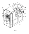
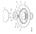
図1は、本発明の実施形態による、1つ又はそれ以上の処理ステーション115を有する加工機又はツール100の等角図である。選択された内部の構成部品を図示するために、処理用ツール100の一部を切り欠いた状態で示されている。この実施形態の1つの態様において、処理用ツール100は、内部領域110を外部領域111から少なくとも部分的に隔離するキャビネット102又は他のエンクロージャを含む。キャビネット102は、複数のアパーチャ106(図1にその1つが見られる)を含み、このアパーチャ106を通して、超小型電子品加工片が、入力/出力ステーション101を介して、内部領域110と外部領域111との間を移動する。1つの実施形態において、入力/出力ステーション101は、各々が加工片コンテナ104をアパーチャ106の近くに配置するように構成された2つのコンテナ支持体105を有する。他の実施形態において、入力/出力ステーション101は、より多数の又はより少数の加工片コンテナ104を支持する。これらの実施形態のいずれかにおいて、加工片コンテナ104は各々、クリーンルーム基準でない他の環境を通して複数の加工片107を支持するのに適した「ミニ」クリーン環境内に、複数の超小型電子品加工片107を収容する。各々の加工片コンテナ104は、処理ステーション115への送出しのために、アパーチャ106を通してキャビネット102の内部領域110からアクセス可能である。
A. Microelectronic products workpiece processing tool Figure 1, according to an embodiment of the present invention is an isometric view of a machine or
処理ステーション115は、洗浄/エッチング・カプセル、アニール・ステーション、測定ステーション、無電解析出ステーション、電解析出ステーション、及び/又は超小型電子品加工片107上でこれら又は他の処理を行うように構成された他のステーションを含む。運搬装置128が、入力/出力ステーション101と処理ステーション115との間で超小型電子品加工片107を移動させる。1つの実施形態において、運搬装置128は、対向する処理ステーション115の列間を内部領域110の長手方向に延びる直線の軌道109を含む。ロボット・ユニット108は、キャビネット102内の処理ステーション115のいずれかにアクセスするために、軌道109に沿って移動する。ツール100の操作は、操作者から命令を受け取ることができ、該命令に基づいて、該ツールの操作を自律的又は半自律的に指示することができるコントローラ112によって制御される。したがって、以下に説明される方法及び操作の一部又は全ては、コンピュータベースのプログラム又はコードによって指示することができる。
The
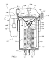
図2は、本発明の実施形態に従って構成された処理ステーション115の1つの概略的な部分断面図である。この実施形態の1つの態様において、処理ステーション115は、超小型電子品加工片107を処理容器130に対して支持する支持部材120を含む。処理容器130内の処理液は、熱伝達装置150及び/又は処理ステーション115の他の機能によって制御される温度である。1つの実施形態において、処理液の温度は、例えば、無電解金属析出プロセスの間、周囲より上に上げられる。したがって、処理液は、一般に、導電性材料を障壁層、形状充填材、及び/又はブランケット層として適用するために用いられる多種多様の無電解処理液のいずれかを含むことができる。別の実施形態において、処理液の温度は、周囲より低く下げられるか、又は周囲より高い最初の高温から周囲より高い低温に下げられる。したがって、熱伝達装置150は、プロセスの要求によって、処理液から及び/又は該処理液に熱を伝達する。これらの実施形態のいずれかにおいて、支持部材120は、処理中に、超小型電子品加工片107を処理液と接触した状態で支持する。
FIG. 2 is a schematic partial cross-sectional view of one of the
この実施形態の1つの態様において、超小型電子品加工片107は、頭部121によって支持され、該頭部121は、頭部支持体122によって支持される。頭部支持体122は、頭部121を処理容器130に対して上下に(矢印130で示されるように)動かす昇降用モータ124aを含む。頭部121内に配置された頭部回転用モータ124bが、頭部支持体122に固定的に取り付けられたシャフトを回転させる。頭部回転用モータ124bが回転すると、頭部121が頭部支持体122に対して回転し(矢印Bで示されるように)、超小型電子品加工片107を(装入取り出しのための)上向き方向と(処理のための)下向き方向との間で移動させる。頭部21は、運搬装置123に連結された加工片回転用モータ124cをさらに含む。矢印Cで示されるように、加工片回転用モータ124cは、運搬装置123を回転させる。
In one aspect of this embodiment, the
1つの実施形態において、運搬装置123は、超小型電子品加工片107を上向き方向に支持するように該超小型電子品加工片107に接触する柱125又は他の保持装置或いは接触部分を含む。この実施形態の1つの態様において、柱125は、超小型電子品加工片107の最外周辺縁部にだけ接触する。この実施形態の別の態様において、柱125は、複数の離間した場所で超小型電子品加工片を支持する。例えば、1つの特定の実施形態において、支持用柱125は、6つの場所で超小型電子品加工片107に接触し、別の実施形態においては、支持用柱125は、7つの場所で超小型電子品加工片107に接触する。更に別の実施形態において、支持用柱125は、より多数の又はより少数の場所で超小型電子品加工片107に接触する。これらの実施形態の更に別の態様において、支持用柱125は、加工片107の裏面の(中央部のような)少なくとも一部が、運搬装置123及びバックプレートのような他の何らかの裏面構造体から離間して配置されるように、該超小型電子品加工片107を支持する。したがって、超小型電子品加工片107の裏面を介して伝達される熱の量を既存の構成より減少させることができる。
In one embodiment, the
上記の実施形態のいずれかにおいて、頭部121は、加工片回転用モータ124cが超小型電子品加工片107を回転させる間、少なくとも前側が処理容器130内の処理液と接触した状態で、該超小型電子品加工片107を支持する。処理の完了後、昇降用モータ124aが頭部121を持ち上げ、任意のすすぎ装置126が加工片107をすすぐ。次に、頭部回転用モータ124bは頭部121を逆にし、伝達装置128(図1)が超小型電子品加工片107を取り出し、処理容器130における処理のために次の超小型電子品加工片107を位置決めすることを可能にする。
In any of the above embodiments, the
本発明の1つの態様において、処理容器130は、該処理容器130の下部の方向に配置された入口部分131に処理液を運ぶ供給用導管133を含む。処理液は、拡散装置140(図10及び図11に関連して以下により詳細に説明される)を通して進み、超小型電子品加工片107に接触する。処理液は、出口部分132で処理チャンバ130を出る。1つの実施形態において、出口部分132は、処理液の自由表面のレベルを定めるせき137を含む。処理液は、せき137の上を進み、外側に延びるスカート134に受けられる。スカート134は、超小型電子品加工片107に接触した後、処理液が下降するオーバーフロー用アパーチャ135を含む。
In one aspect of the present invention, the
この実施形態の更に別の態様において、熱伝達装置150が、処理容器130内の処理液の温度を制御するように、該処理容器130と熱的に接触した状態で配置される。この実施形態の特定の態様において、熱伝達装置150は、処理容器130のせき137を超えて進む処理液を集める、上部入口部分を有する熱伝達容器又はリザーバ153を含む。処理容器130から受けた処理液は、別の入口部分151を通して熱伝達容器153に導入された付加的な処理液と混合する。図7に関連して以下に詳細に説明されるように、1つの実施形態において、入口部分151を通して入る付加的な処理液は、熱伝達容器153から遠く離れて配置された付加的な熱伝達装置によって温度制御される。付加的な処理液との間で遠く離れて熱を伝達することに加えて又は代わりに、以下に説明されるように、別の実施形態において、処理液が熱伝達容器153内にある間に、付加的な処理液を含む処理液との間で熱が伝達される。同じく図7に関連して以下により詳細に説明されるように、少なくともこれらの実施形態の一部の更に別の態様において、処理液は、出口部分152を通して熱伝達容器153から取り除かれ、再利用される。熱伝達容器153内の液体レベルを判断するために、センサ・ポート167がセンサに連結される(図2には図示されていない)。
In yet another aspect of this embodiment, the
1つの実施形態において、熱伝達容器153は、該熱伝達容器153内の処理液との間で熱を直接伝達する熱交換器166を含む。この実施形態の1つの態様において、熱交換器166は、熱伝達用流体が通る1つ又はそれ以上の熱交換用導管154を含む。この実施形態の別の態様において、熱伝達用流体は、脱イオン水(0℃から100℃までの温度に適している)、或いはエチレン・グリコール、グリセロール、フッ化化合物、又はオイル(より高い温度又はより低い温度に適している)を含む。脱イオン水は、約40℃から約80℃までの温度で行われる一般的な無電解めっきプロセスに適している。これらの実施形態のいずれかにおいて、熱交換用導管154は、熱交換用入力ポート156で熱伝達容器153に入り、熱交換用出力ポート157で出ていく。
In one embodiment, the
この実施形態の更に別の態様において、熱交換用導管154が、供給用導管133に極めて近接して熱交換用支持体155上に支持され、熱交換用導管154と供給用導管154内の処理液との間で熱を伝達する効率を改善する。この実施形態の更に別の態様において、熱交換用導管154は、供給用導管133を囲む螺旋形又は他の回旋状の経路を有し、該供給用導管133もまた、熱伝達容器153を通して処理容器133に進む時に螺旋形又は他の回旋状の経路を有する。他の実施形態において、熱交換用導管154及び/又は供給用導管133は、熱伝達に利用可能な表面積を増加させる他の構成をもつこともできる。例えば、1つの実施形態において、熱交換用導管154及び/又は供給用導管133は、熱伝達用フィンを含む。他の実施形態において、熱伝達容器153内の処理液は、他の構成に従って加熱又は冷却される。例えば、1つの特定の実施形態において、熱交換器166は、熱交換用導管154の代わりに、(被覆された、及び/又は他の方法で処理液との接触から保護された)電気抵抗加熱器を含む。図4及び図5に関連して以下により詳細に説明されるように、更に別の実施形態において、内部装置ではなく外部装置によって、熱伝達容器153との間で熱が伝達される。熱伝達用フィンのない単純な流体含有供給用導管133の利点は、これが、局所的に高い(又は低い)温度領域を有する傾向が少ない点である。こうした領域により、処理液内の導電性材料が外部にめっきされることがある。
In yet another aspect of this embodiment, a
上記の実施形態の何れかにおいて、熱交換用導管154は、供給用導管133内の処理液との間だけでなく、該供給用導管133及び熱伝達容器153内の処理液との間でも、熱を伝達する。熱伝達容器153内の処理液は、処理容器130の容器壁136を通して、該処理容器130内の処理液との間で熱を伝達する。したがって、この実施形態の1つの態様において、容器壁136は、薄く及び/又は熱伝導性の高い、或いは他の方法で熱透過型のものであり、内部の処理液との間で熱が伝達される効率を改善する。
In any of the above embodiments, the
図3は、図2に関連して上述されたものにほぼ類似した処理ステーションの、上から見た部分拡大等角図である。この実施形態の1つの態様において、処理ステーション115は、該処理ステーション115をツール100(図1)に取り付けるための取り付けプレート117を含む。処理ステーション115は、処理容器130内に存在し得る気泡を運び去る排出プレナム116をさらに含む。こうした気泡は、超小型電子品加工片107(図2)において完了した処理を妨げるものである。
図3に示される実施形態の1つの態様において、排出プレナム116、処理容器130、及び拡散装置140は、処理ステーション115から容易に取り外されるように構成される。したがって、熱交換用支持体155及び該熱交換用支持体155が支持する熱交換用導管154(図2)は、洗浄、及び/又は他のルーチンの点検及び/又は保守のために、熱伝達容器153から容易に取り外すことができる。
FIG. 3 is a partially enlarged isometric view from above of a processing station substantially similar to that described above in connection with FIG. In one aspect of this embodiment, the
In one aspect of the embodiment shown in FIG. 3, the
図4は、本発明の別の実施形態による、熱伝達容器450及び熱交換器466を有する処理ステーション415の部分的に概略的な、部分的に切り欠いた等角図である。本発明の1つの態様において、処理ステーション415は、図2に関連して上述されたものにほぼ類似した処理容器130を含む。熱伝達装置450は、処理容器130内の処理液との間で熱を伝達し、該処理容器130のせき137から溢れ出る処理液を集めるように、処理容器130から外側に配置された第1の熱伝達容器453aを含む。(第1の熱伝達容器453a内の処理液を加熱又は冷却する)熱交換器466は、該第1の熱伝達容器453aから外側に配置された第2の熱伝達容器453bを含む。第2の熱伝達容器453bは、処理液から別個に熱伝達用流体を受け取る、及び/又は該処理液と異なる熱伝達用流体を受け取る入口部分451を含む。熱伝達用流体は、第2の熱伝達容器453bを通して、出口部分452に進み、該出口部分452に進むにつれて、第1の熱伝達容器453a内の処理液に熱を伝達する。処理ステーション415は、第1の熱伝達容器453aと第2の熱伝達容器453bとの間の間隙領域内にバッフル又はフィン458を含み、該第2の熱伝達容器453bを通して熱伝達用流体の流れを制御し、及び/又は該熱伝達用流体と第1の熱伝達容器453aとの間で伝達される熱の量を増加させる。
FIG. 4 is a partially schematic, partially cut away isometric view of a
図5は、本発明の別の実施形態に従って構成された処理ステーション515の部分概略図である。この実施形態の1つの態様において、処理ステーション515は、図2に関連して上述された処理容器130及び熱伝達容器153とほぼ同様に構成された処理容器130及び熱伝達容器153を含む。熱交換器566が、熱伝達容器153から外側に配置され、該熱伝達容器153内の処理液を加熱又は冷却する。この実施形態の1つの態様において、熱交換器566は、熱伝達容器453と熱的に接触した状態で熱伝達用流体を運ぶ導管を含む。別の実施形態において、熱交換器566は、同じく熱伝達容器153と熱接触した状態で配置された電気抵抗加熱器を含む。
FIG. 5 is a partial schematic diagram of a
図6は、本発明の別の実施形態に従って構成された処理ステーション615の一部の、部分的に概略的な、部分断面側面図である。この実施形態の1つの態様において、処理ステーション615は、処理液を受ける入口部分631と、処理液が処理容器630を出ていく出口部分632とを有する処理容器630を含む。出口部分632は、図2に関連して上述されたものにほぼ類似した方法で進むせき637を含む。オーバーフロー用アパーチャ636が、せき637を越えた処理液を受ける。次に、処理容器630から出た処理液は、再利用されるか又は廃棄される。
FIG. 6 is a partially schematic, partial cross-sectional side view of a portion of a
処理ステーション615の実施形態は、処理容器630の円錐状の容器壁636から外側に配置され、該容器壁636に隣接した熱伝達装置650をさらに含む。この実施形態の1つの態様において、熱伝達装置650は、容器壁636の周りの螺旋形の経路内の熱伝達用流体を運ぶ導管654を含む。別の実施形態において、熱伝達装置650は、処理容器630内の処理液を加熱するのにほぼ類似した方法で配置された電気抵抗加熱器を含む。他の実施形態において、熱伝達装置650は、内部の処理液との間で容器壁636を通して熱を伝達するように配置された他の構成を含む。
An embodiment of the
この実施形態の別の態様において、処理容器630は、内部の処理液からの熱損失の可能性を減少させるために、比較的小さな容積を有するものである。例えば、1つの実施形態において、処理容器630は、200mm(20cm)の直径の超小型電子品加工片107を受けるような大きさに作られ、約100cm3又はそれより少ない容積を有する。特定の実施形態においては、処理容器630は、約20cm3の容積を有する。別の実施形態においては、処理容器630は、(200mmの直径の超小型電子品加工片107上に1mmの厚さの流体層を形成するのに十分な)約32cm3の容積を有する。したがって、1つの実施形態において、加工片の直径の3乗と処理容器630の容積の比は、約80(100cm3の容積の場合)から約400(20cm3の容積の場合)までの範囲を有する。他の実施形態において、容器630は、例えば、処理液についての金属欠乏の目標レベルによって、他の容積を有する。例えば、比較的低い金属イオン濃度をもった処理液を有する、単一の200mmの加工片上に、100Åのコバルト・タングステン・リン合金層を析出させる時、処理液内の金属は、処理容積が2.3cm3の場合には完全に使い果たされ、処理容積が22cm3の場合には10%使い果たされ、処理容積が44cm3の場合には5%使い果たされる。
In another aspect of this embodiment, the
1つの実施形態において、比較的小さい容積を有する処理容器630は、無電解又は他の処理液を用いる使い捨て処理に適したものである。この実施形態の1つの態様による方法は、第1の量の処理液を処理容器630内に指向させ、超小型電子品加工片107を下げて、処理のために処理液と接触させ、該超小型電子品加工片107を該処理液から取り出す段階を含む。次に、第1の量の処理液が処理容器630から取り出され、次の超小型電子品加工片107の処理前に、新たな第2の量の処理液と交換される。上記の方法は、金属を超小型電子品加工片107の上に無電解により析出するのに特に適しており、処理液の(化学的性質のような)特徴が安定していないもののような他の処理にも適している。
In one embodiment, the
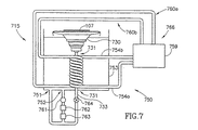
図7は、本発明の別の実施形態による熱伝達機能及び流れ機能の構成を有する処理ステーション715の概略図である。この実施形態の1つの態様において、処理ステーション715は、図2に関連して上述されたものにほぼ類似した方法で、処理液が熱伝達容器753内に溢れ出るように配置された処理容器730を含む。処理容器730には、供給用導管733によって処理液が供給され、この供給用導管733は、説明のために図7では直線の導管として示されるが、図2に関連して上述された供給用導管133にほぼ類似した回旋形状又は螺旋形状を有することができる。
FIG. 7 is a schematic diagram of a
この実施形態の1つの態様において、処理ステーション715は、供給用導管733内の処理液を加熱又は冷却するための熱伝達装置750を含む。熱伝達装置750は、熱伝達容器753と熱交換器766とを含む。熱交換器766は、(第1の回路760a及び第2の回路760bとして図7に示される)2つの回路760を通過する熱伝達用流体を加熱又は冷却するための熱伝達容器753の外側に配置された加熱器759を含む。各々の回路760は、熱交換用導管754(第1の熱交換用導管754a及び第2の熱交換用導管754bとして示される)を含む。第1及び第2の回路760a、760bは、逆流熱交換器構成を有する。したがって、第1の熱交換用導管754aは、熱伝達容器753に入って底部に向かい、該熱伝達容器753を出て上部に向かう。第2の熱交換用導管754bは、熱伝達容器753に入って上部に向かい、該熱伝達容器753を出て底部に向かう。その結果、熱伝達容器753及び供給用導管733の両方の内容物が均一に加熱又は冷却される。他の実施形態において、熱伝達装置750は、処理液の流量及び許容温度偏差といった特定の要件によって、2つより多いか又は少ない回路を含む。
In one aspect of this embodiment, the
この実施形態の別の態様において、熱伝達容器753内の処理液が、出口部分752で該熱伝達容器753から取り出される。処理液は、ポンプ761、フィルタ762、及び任意に直列型熱交換器763を通して進む。次に、処理液は、処理容器730の入口部分731及び熱伝達容器753の入口部分751の両方に提供される。弁又は制限装置764により、処理液が処理容器730の入口部分731を通して進む速度が調整される。ポンプ761が一定の速度で作動する時、弁764を通る流量を減らすことは、熱伝達容器753の入口部分751を通る流量を増加させ、該弁764を通る流量を増やすことは、反対の効果を有する。別の代替的な構成において、別個の弁が、処理容器730及び熱伝達容器753への流れを個別に制御する。いずれの実施形態においても、処理容器730及び/又は熱伝達容器753への流量は、所望の温度均一性と共に、超小型電子品加工片107における所望の流量をもたらすように選択される。
In another aspect of this embodiment, the processing liquid in the
幾つかの場合、処理容器730に入る所望の処理液の流量は非常に少ないものなので、処理液の自由表面から熱が失われる速度は、熱伝達装置750及び直列型熱交換器763によって熱が加えられる速度を超える。これらの場合、本発明の実施形態による方法は、処理容器内の処理液の温度における比較的小さい受容可能な変化を可能にしながら、非常に少ない処理液の流量で1つ又はそれ以上の超小型電子品加工片107を処理する段階を含む。次に、処理容器730は速い流速で流され、次の超小型電子品加工片107が処理される前に所望の処理温度で新たな処理液を導入する。
In some cases, the flow rate of the desired process liquid entering the
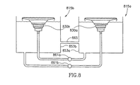
図8は、各々が、図2に関連して上述された処理容器130にほぼ類似した(第1の処理容器830a及び第2の処理容器830bとして示される)処理容器830を有する、(第1の処理ステーション815a及び第2の処理ステーション815bとして示される)一対の処理ステーション815の概略図である。処理液は、処理容器830a、830bから、対応する熱伝達容器853a、853b内に進む。第1のポンプ861aが、処理液を第1の熱伝達容器853aから第2の処理容器830b内に指向させ、第2のポンプ861bが、処理液を第2の熱伝達容器853bから第1の処理容器830a内に指向させる。各々の熱伝達容器853a、853b内の処理液を一定レベルに維持するために、均等化チャネル865が、該熱伝達容器853aと853bの間に連結される。この構成の1つの特徴は、処理容器830及び熱伝達容器853を交差連結することによって、各々の処理容器830a、830bの中の処理液の温度をほぼ同じにすることができる点である。この特徴の利点は、各容器830a、830b内で処理される超小型電子品加工片107が、ほぼ同じ処理条件の影響下におかれ、処理される超小型電子品加工片により大きい均一性がもたらされることである。
FIG. 8 includes a processing vessel 830 (shown as a
図9は、本発明の別の実施形態による、供給弁組立体970から複数の処理液を受け取る処理容器930を有する処理ステーション915の概略図である。この実施形態の1つの態様において、処理容器930は、処理液を受けるために供給弁組立体970に連結された入口部分931を含む。(熱伝達容器953のような)熱伝達装置950は、上述のものとほぼ類似した方法で、処理容器930との間で熱を伝達する。供給弁組立体970は、連続的な操作段階中に異なる処理液を処理容器930に連続的に供給するように3つの供給弁971(図9にその2つが見られる)を支持する単一のハウジングを含む。処理液の1つのための源990が図9に概略的に示され、この源990は、処理液を加熱又は冷却するために(熱伝達用流体導管のような)熱伝達装置991を含む。供給弁組立体970をより完全に排水するために、供給弁971の下に排出弁972が配置される。熱伝達容器953は、1つの実施形態において、該熱伝達容器953を出る処理液を分離するように、供給弁970のものにほぼ類似した構成を有する弁組立体に連結された出口部分952を含む。
FIG. 9 is a schematic diagram of a
この実施形態の1つの態様において、単一のハウジングが、多数の処理液を単一の処理容器930に連続的に供給する。別の実施形態において、各々が別個の弁を有する複数のハウジングが、対応する複数の処理液を供給するために互いに連結される。これらの実施形態のいずれかにおいて、単一の処理容器930には、対応する複数の化学プロセスを実行するために複数の処理液が供給される。したがって、単一の処理容器930を用いて、材料の析出、材料の除去、洗浄のような作業、及び/又は超小型電子品加工片における他のプロセスを実行することができる。多数のポートをもつ供給弁組立体970は、処理容器930を洗浄液の源に選択的に連結するのにも適している。したがって、処理容器930を取り外すことなく、(例えば、処理液によってめっきすること、又は他の方法で該処理液から析出する化学物質の析出物を除去することによって)処理容器930を洗浄することができる。他の実施形態において、例えば、大処理量要求により、同時に処理されることになる種々の超小型電子品加工片が必要とされる時、ツール100(図1)は、各々が別個の処理の源に連結された複数の処理容器を含む。
In one aspect of this embodiment, a single housing continuously supplies multiple processing liquids to a
図1乃至図9に関連して上述された処理ステーションの特定の実施形態の1つの特徴は、処理容器が薄い及び/又は熱伝導性の壁を有することである。この構成の利点は、処理容器内の処理液が、該処理容器の外側の領域から熱を受け取り又は該処理容器の外側の領域に熱を放散して、該処理液の自由表面において、及び/又は超小型電子品加工片との接触によって失われた又は得られた熱をオフセットさせるという点である。したがって、処理液の温度、特に超小型電子品加工片との界接面における処理液の温度は、均一な処理結果のために安定したレベルに維持される。この構成の別の利点は、一定の温度で処理液を維持することによって、高温及び/又は低温の区域を減少及び/又は排除できることであり、このことは、処理液から導電性材料をめっきする可能性を減少させることができる。 One feature of certain embodiments of the processing station described above in connection with FIGS. 1-9 is that the processing vessel has thin and / or thermally conductive walls. The advantage of this configuration is that the processing liquid in the processing vessel receives heat from or dissipates heat from the region outside the processing vessel to the free surface of the processing solution and / or Alternatively, the heat lost or gained by contact with the microelectronic workpiece is offset. Therefore, the temperature of the processing liquid, particularly the temperature of the processing liquid at the interface with the microelectronic product workpiece is maintained at a stable level for a uniform processing result. Another advantage of this configuration is that by maintaining the treatment liquid at a constant temperature, high and / or low temperature areas can be reduced and / or eliminated, which is the plating of the conductive material from the treatment liquid. The possibility can be reduced.
図1乃至図9に関連して上述された処理ステーションの特定の実施形態の別の特徴は、処理液と超小型電子品加工片との間の界接面の近くの領域における処理容器との間で熱を伝達するために、熱伝達装置が該処理容器のすぐ近くに配置されるという点である。この構成の利点は、この界接面における処理液の温度をより正確に制御できることである。特定の実施形態において、熱伝達装置は、処理容器を出る処理液も受け取る。この構成の利点は、熱伝達装置が、処理液及び/又は超小型電子品加工片の界接面(上述のような)に極めて接近した状態で該処理液を加熱又は冷却するだけでなく、処理液のためのリザーバとして働く点である。 Another feature of the specific embodiment of the processing station described above in connection with FIGS. 1-9 is that the processing vessel in the region near the interface between the processing liquid and the microelectronic workpiece is In order to transfer heat between them, a heat transfer device is arranged in the immediate vicinity of the processing vessel. The advantage of this configuration is that the temperature of the treatment liquid at this interface can be controlled more accurately. In certain embodiments, the heat transfer device also receives processing liquid exiting the processing vessel. The advantage of this configuration is that the heat transfer device not only heats or cools the processing liquid while in close proximity to the processing liquid and / or the interface of the microelectronic workpiece (as described above), It is a point that serves as a reservoir for the treatment liquid.
上記の特徴は、超小型電子品加工片で実行される処理の温度感性が高い場合に特に有利である。こうしたプロセスの1つの例は、超小型電子品加工片上への導電性材料の無電解析出である。1つの特定の例は、(コバルト、ニッケル、又はその合金のような)障壁金属を、パターン形成された(例えば、化学機械平坦化後の)超小型電子品加工片上にめっきすることである。別の特定の例は、導電性材料のブランケット層及び/又は充填材層を超小型電子品加工片の上に析出させることを含む。無電解処理液の化学的安定性及び/又は無電解により析出された材料の析出速度の両方とも、温度感性が高い傾向があり、処理液の温度を正確に制御することによって、優れた結果が得られる。電解析出法プロセスのような他のプロセスにおいても、処理液の温度を正確に制御することが有利である。例えば、電解処理液は、広範囲の温度において安定したままであるが、これらの液体が材料を超小型電子品加工片に適用する速度は、温度に左右され得る。したがって、材料が電解によって超小型電子品加工片に適用される速度(よって、潜在的に均一性)は、電解処理液の加熱及び/又は冷却を通して温度を制御することによって、制御することができる。
他の実施形態において、図1乃至図9に関連して上述されたものにほぼ類似した装置が、超小型電子品加工片を処理するための他のプロセスで用いられる。こうしたプロセスには、加工片の洗浄及び/又はエッチング、及び/又は析出、及び/又は超小型電子品加工片から(フォトレジストのような)導電性材料以外の材料を取り除くことが含まれる。
The above features are particularly advantageous when the temperature sensitivity of the process performed on the microelectronic product workpiece is high. One example of such a process is the electroless deposition of a conductive material onto a microelectronic workpiece. One particular example is plating a barrier metal (such as cobalt, nickel, or an alloy thereof) onto a patterned microelectronic workpiece (eg, after chemical mechanical planarization). Another specific example includes depositing a blanket layer and / or filler layer of conductive material on a microelectronic workpiece. Both the chemical stability of the electroless treatment liquid and / or the deposition rate of the material deposited by electroless tend to be high in temperature sensitivity, and by controlling the temperature of the treatment liquid accurately, excellent results can be obtained. can get. In other processes such as the electrolytic deposition process, it is advantageous to accurately control the temperature of the treatment liquid. For example, electrolytic treatment liquids remain stable over a wide range of temperatures, but the rate at which these liquids apply material to microelectronic workpieces can be temperature dependent. Thus, the rate at which the material is applied to the microelectronic workpiece by electrolysis (and thus the potential uniformity) can be controlled by controlling the temperature through heating and / or cooling of the electrolytic treatment solution. .
In other embodiments, an apparatus generally similar to that described above in connection with FIGS. 1-9 is used in other processes for processing microelectronic workpieces. Such processes include cleaning and / or etching and / or deposition of the workpiece and / or removing materials other than conductive materials (such as photoresist) from the microelectronic workpiece.
B.処理液のための流れ拡散装置
図10は、本発明の実施形態による、処理容器130内に配置された拡散装置140の部分展開等角図である。この実施形態の1つの態様において、拡散装置140は、拡散装置カップ1042内に取り外し可能に配置された拡散装置本体1080を含む。拡散装置カップ1042は、拡散装置本体1080と協働して、入口ポートと1081を通して該拡散装置本体1080に入り、液体のためのプレナム1084を定めるカップ壁1044を含む。処理液は、拡散装置本体1080を通して進み、一次出口ポート1082及び/又は1つ又はそれ以上の二次出口ポート1083を通して出ていく。したがって、拡散装置本体1080は、処理液を超小型電子品加工片107の方向に指向させる。本発明の特定の態様において、処理液は無電解処理液であり、よって電極がない場合には超小型電子品加工片107に向けられる。
B. Flow Diffusion Device for Processing Liquid FIG. 10 is a partially exploded isometric view of a
図11は、図10に示される拡散装置140の実施形態の断面図である。この実施形態の1つの態様において、処理液は、1つ又はそれ以上の入口ポート1081を通してプレナム1084内に進む。プレナム1084内の処理液のある部分は、一次流路1085を通して一次出口ポート1082に進む。処理液の別の部分は、二次流路1086を通して二次出口ポート1083に進む。
この実施形態の1つの態様において、拡散装置本体1080は、対で配置された複数の一次流路1085を含み、対向する一次流路1085が、処理液のそれぞれの部分を互いに向けて指向させる。この特徴の利点は、一次流路1085が該一次出口ポート1082の対向する壁のような他の構造体に直接当たる場合より、一次出口ポート1082を通過する流れを均一にできる点である。
FIG. 11 is a cross-sectional view of the embodiment of the diffusing
In one aspect of this embodiment, the diffusing
1つの実施形態において、入口部分ポート1081、一次流路1085、及び二次流路1086は、ほぼ円形の断面形状を有する。他の実施形態において、これらの特徴は、弧状又はスロット型の形状を有することができる。これらの実施形態のいずれかにおいて、プレナム1084から超小型電子品加工片107の方向に進む流れのかなりの部分が、一次出口ポート1082を通して進む。例えば、この実施形態の1つの態様において、処理の総量の約20%から約50%までが、一次出口ポート1082を通して進む。したがって、一次出口ポート1082の流れ面積は、該一次出口ポート1082及び全ての二次出口ポート1083の総流れ面積の約20%から約50%までになる。
この実施形態の別の態様は、二次流路1086及び二次出口ポート1083が、一次出口ポート1082の中心軸1087から外側に傾斜しているというものである。前記の特徴の利点は、超小型電子品加工片107上に衝突する流れが、別個の噴流の形態で衝突する可能性が低く、均一の上昇流の形態で衝突する可能性がより高いことである。この利点は、温度依存プロセス、及び/又は超小型電子品加工片107との界接面における処理液の特性(流速及び温度のような特性)が、所望のプロセスの結果として均一になるために、他のプロセスにとって特に重要なものになり得る。
In one embodiment, the
Another aspect of this embodiment is that the
C.超小型電子品加工片の予熱及び/又は後加熱、及び/又は冷却
図12は、本発明の実施形態による、予熱、予冷却、後加熱、及び/又は後冷却されるように配置された、図2に関連して上述された処理ステーション115の部分概略図である。この実施形態の1つの態様において、例えば、処理容器130内の処理液が周囲温度及び超小型電子品加工片107の初期温度より上に加熱される場合には、該超小型電子品加工片107は、処理液と接触する前に予熱される。したがって、頭部121は、処理容器130内の処理液の自由表面1238に対して離間配置された位置に超小型電子品加工片107を支持し、該超小型電子品加工片107が、処理液と接触する前に熱平衡に近づく及び/又は熱平衡に達することを可能にする。
C. Preheating and / or post-heating of microelectronic products workpiece, and / or cooling Figure 12, according to an embodiment of the present invention, preheating, precooling, it arranged to be post-heating, and / or post-cooling, FIG. 3 is a partial schematic view of the
この実施形態の1つの態様において、頭部121は、超小型電子品加工片107が処理容器130内の処理液の温度になるか又は処理液の温度付近になるまで、選択された時間の間動かないままである。例えば、特定の実施形態において、頭部121は、数秒から60秒又はそれより長い範囲にわたる時間動かないままである。別の実施形態において、頭部121は、超小型電子品加工片107が、処理液と接触するために該処理液との熱平衡に近づくか又は熱平衡に達することを可能にするのに十分に遅い速度で下方に移動する。どちらの実施形態の特徴も、超小型電子品加工片107が処理液と接触する時に、該処理液に熱的に衝撃を与える可能性が少ないことである。したがって、処理液は、処理中により一定の温度で維持されることになり、このことは、その後のプロセス中に得られる結果の品質及び/又は均一性を改善する。
In one aspect of this embodiment, the
別の実施形態において、前記のステップを逆にし、超小型電子品加工片が処理液と接触した後に、制御された方法で該超小型電子品加工片107を冷却することができる。この実施形態の1つの態様において、超小型電子品加工片107は、処理容器130の上に静止した状態で保持されるか、該処理容器130から遠ざかるようにゆっくりと移動され、該超小型電子品加工片107が該処理容器130を囲む環境と徐々に熱平衡状態になることを可能にする。
図12に関連して上述された前記の実施形態の1つの態様において、超小型電子品加工片107は、該超小型電子品加工片107を予熱のために処理する前、及び/又は該超小型電子品加工片107を冷却するために処理した後、処理容器130の上に配置される。別の実施形態において、例えば、処理容器130内の処理容器が周囲より下の温度である時、同じ技術を用いて、処理前に超小型電子品加工片107を予冷却し、及び/又は該超小型電子品加工片107の温度が処理後に上がることを可能にする。
In another embodiment, the above steps can be reversed to cool the
In one aspect of the above-described embodiment described above in connection with FIG. 12, the
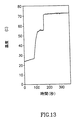
図13は、図12に関連して上述されたものとほぼ類似した方法で超小型電子品加工片107を予熱する時間の関数として、該超小型電子品加工片107の平均温度を示すグラフである。ここで図12及び図13を参照すると、1つの実施形態において、超小型電子品加工片107は、時間T=0から約T=90秒まで、頭部121内に上向きに配置される。T=90秒において、頭部121は回転して超小型電子品加工片107を反対にし、処理液の近くであるが該処理容器から離間した状態で該超小型電子品加工片107を位置決めする。T=90秒から約T=150秒まで、超小型電子品加工片は、処理液の上に置かれたままである。この間に、超小型電子品加工片107の温度は、約25℃から約55℃まで上がる。T=150秒において、超小型電子品加工片は、約72℃の温度で処理するために、処理液と接触するように下げられる。他の実施形態において、上述の時間セグメント(例えば、T=0からT=90秒まで、及びT=0からT=150までのような)は、著しく減少され、超小型電子品加工片が予熱及び/又は予冷却するのを依然として可能にしながら、全体の処理時間が減少される。
FIG. 13 is a graph showing the average temperature of the
D.加工片の温度の均一性及び/又は析出の均一性
本発明の別の実施形態による方法において、処理液と接触した状態で超小型電子品加工片107(図2)の回転速度を制御し、該超小型電子品加工片107の表面における温度及び/又は温度分布を制御することができる。図14A乃至図14Cは、回転速度が増大された時に超小型電子品加工片107の表面にわたる温度均一性の増大を予測する数値的なシミュレーションの結果である。回転する超小型電子品加工片によって引き起こされる遠心ポンプ効果を説明するために、このシミュレーションは、超小型電子品加工片107の表面に処理液を提供する速度を増大させる段階を含む。
D. Uniformity of workpiece temperature and / or deposition uniformity In a method according to another embodiment of the present invention, the rotational speed of the microelectronic workpiece 107 (FIG. 2) is controlled in contact with the processing liquid; The temperature and / or temperature distribution on the surface of the microelectronic product processed
図14Aは、2rpmの超小型電子品加工片回転速度及び1分あたり1リットルの処理液の流量についての予測結果を示す。超小型電子品加工片107が処理液に接触する時に、ライン1490aは、該超小型電子品加工片の縁部における時間の関数として、温度応答を示す。ライン1492aは、超小型電子品加工片107の中心における温度応答を示し、ライン1491aは、超小型電子品加工片107の縁部と中心の間の中点における温度応答を示す。
図14Bは、10rpmの加工片回転速度及び1分あたり2リットルの処理液の流量についての予測結果を示す。図14Bに示されるように、超小型電子品加工片の縁部及び中点における温度応答(それぞれライン1490b及び1491b)は、互いにつぶれており、両方とも加工片の中心における温度応答(ライン1492b)に接近している。図14Cに示されるように、20rpmの加工片回転速度及び1分あたり3リットルの処理液の流量において、超小型電子品加工片107の3つの領域全て(1490c、1491c、及び1492cで示される)が互いにつぶれている。図14A乃至図14Cに関連して上述された方法の実施形態の1つの特徴は、超小型電子品加工片107を回転させる速度を増大させることによって、超小型電子品加工片107の表面の温度をより迅速かつ均一に一定値にもっていくことができる点である。この実施形態の1つの態様において、回転速度を20rpmまで上げ、温度応答の均一性を高めることができる。他の実施形態において、例えば、処理液が他の温度及び/又は他の特性を有する場合には、他の回転速度を用いて同じ又は類似した結果を達成することができる。これらの実施形態にいずれかにおいて、回転速度は、最初に比較的高くし(例えば、超小型電子品加工片が、処理液との熱平衡に達するか又は少なくとも接近するまで)、次に、例えば、低い回転速度が次のプロセスにより適している場合に減少される。
FIG. 14A shows the prediction result about the rotation speed of the micro-electronic article processed piece of 2 rpm and the flow rate of the processing liquid of 1 liter per minute. As the
FIG. 14B shows prediction results for a workpiece rotation speed of 10 rpm and a flow rate of 2 liters of processing liquid per minute. As shown in FIG. 14B, the temperature response at the edge and midpoint of the microelectronic workpiece (
E.回転速度を用いて大量輸送の均一性及び/又は析出の均一性を制御する
本発明の別の実施形態による方法は、処理液と接触した状態で超小型電子品加工片107が回転する速度を制御することによって、該超小型電子品加工片107(図2)の上に析出された材料の分布のような特性を制御するステップを含む。この実施形態の1つの態様において、超小型電子品加工片107に適用される材料の厚さ形状は、該超小型電子品加工片の回転速度を制御することによって制御される。例えば、1つの特定の実施形態において、超小型電子品加工片107を回転させる速度は、該超小型電子品加工片107に材料を均一に適用するか、又は該加工片107の中心又は周囲のいずれかに材料をより迅速に適用するように制御される。この実施形態の1つの態様において、加工片107の縁部よりも該加工片107の中心で材料をより迅速に適用するように、200ミリメートルの直径を有する超小型電子品加工片107が、(1rpmのような)非常に低い速度で回転される。加工片の回転速度が増大するにつれて、中間の回転速度(例えば、約50rpm)で、材料が該加工片107にわたって均一の速度で適用されるまで、材料適用速度の均一性も増す。回転速度がさらに増すと、材料は、例えば、約100rpmの回転速度においては、加工片107の中央領域より該加工片107の周辺領域に、より迅速に適用されることになる。
E. A method according to another embodiment of the present invention that uses rotational speed to control the uniformity of mass transport and / or the uniformity of precipitation, the speed at which the
上前記の実施形態の1つの態様において、コバルト合金(コバルト、タングステン、及びリンのような)のための無電解析出溶液が、約0.5lpmから約1lpmまでの速度の、約73℃の無電解プロセスにおいて適用される。他の実施形態において、この方法は、優先的に異なる材料を適用し、及び/又は優先的に材料を超小型電子品加工片の異なる部分に適用するように、異なる化学化合物、異なる流量(例えば、約5lpmまで)、及び/又は回転速度を選択するステップを含む。
上記から、説明のために本発明の特定の実施形態をここに説明するが、本発明の精神及び範囲から逸脱することなく種々の修正をなし得ることが理解されるであろう。したがって、本発明は、添付の特許請求の範囲によるものを除き、制限されるものではない。
In one aspect of the above embodiment, an electroless deposition solution for a cobalt alloy (such as cobalt, tungsten, and phosphorus) has a rate of about 73 ° C. at a rate from about 0.5 lpm to about 1 lpm. Applied in electrolysis process. In other embodiments, the method preferentially applies different materials and / or preferentially applies the material to different parts of the microelectronic workpiece, such as different chemical compounds, different flow rates (e.g. , Up to about 5 lpm), and / or selecting a rotational speed.
From the foregoing, it will be understood that, although specific embodiments of the invention are described herein for purposes of illustration, various modifications may be made without departing from the spirit and scope of the invention. Accordingly, the invention is not limited except as by the appended claims.
Claims (33)
前記処理液を受けるように配置された入口部分と、容器を出ていく処理液を通すように配置された出口部分と、容器の外側の第1の領域と容器の内側の第2の領域との間で熱を伝達するように構成された熱透過型容器壁とを有し、処理液を支持するように構成された容器と、
前記第1の領域内に配置され、前記容器壁との間で熱を伝達するように該容器壁に熱的に連結された熱伝達装置と、
を備えることを特徴とする装置。 An apparatus for processing a micro-electronic work piece,
An inlet portion arranged to receive the treatment liquid, an outlet portion arranged to pass the treatment liquid exiting the container, a first region outside the container, and a second region inside the container A heat permeable container wall configured to transfer heat between and a container configured to support the processing liquid;
A heat transfer device disposed in the first region and thermally coupled to the vessel wall to transfer heat to and from the vessel wall;
A device comprising:
前記第1の容器の前記入口部分に連結された、前記第2の容器内の処理液と熱的に連通している回旋状の供給用導管をさらに備え、前記回旋状の供給用導管を通して該第1の容器に進む処理液が該第2の容器内の処理液から熱を受け取り、該供給用導管は、該第2の容器に連結されて、該第2の容器において受け取った処理液を再利用するようになり、
前記超小型電子品加工片をすすぐために前記第1の容器の上に配置されたすすぎ装置が設けられたことを特徴とする請求項1に記載の装置。 The container is a first container, and the heat transfer device includes a second container, and the first container is received in the second container after overflowing the cough of the first container. Is disposed in the second container so as to be in thermal communication with the processing liquid, and the second container receives the processing received from the first container. Forming an integral reservoir for liquid, said device comprising:
A convoluted supply conduit connected to the inlet portion of the first container and in thermal communication with the processing liquid in the second container; and through the convoluted supply conduit The processing liquid traveling to the first container receives heat from the processing liquid in the second container, and the supply conduit is connected to the second container to receive the processing liquid received in the second container. To reuse,
The apparatus of claim 1, further comprising a rinsing device disposed on the first container for rinsing the microelectronic workpiece.
超小型電子品加工片を受けるように配置された入力/出力ステーションと、
前記処理ステーションの間で超小型電子品加工片を移動させるように配置された運搬装置と、
をさらに備えることを特徴とする請求項1に記載の装置。 The container is disposed in one of a plurality of processing stations, and the apparatus comprises:
An input / output station arranged to receive a microelectronic workpiece;
A transport device arranged to move microelectronic workpieces between said processing stations;
The apparatus of claim 1, further comprising:
前記横断方向の寸法の3乗と前記容器容積の比が約80より大きいことを特徴とする請求項1に記載の装置。 A container volume configured to support a processing liquid having a free surface and further configured to receive a microelectronic workpiece having a generally transverse dimension in the plane of the free surface; Have
The apparatus of claim 1, wherein the ratio of the cube of the transverse dimension to the container volume is greater than about 80.
前記第1の容器の前記入口部分が、前記リザーバ内に位置する入口を含み、
前記第1の容器が、前記入口に連結された第1の供給用導管を含み、
前記第2の容器が、第2の供給用導管と、前記リザーバの底部に向けて配置されたドレインとを含む、
ことを特徴とする請求項2に記載の装置。 The second container includes a reservoir disposed around and below the first container;
The inlet portion of the first container includes an inlet located in the reservoir;
The first container includes a first supply conduit coupled to the inlet;
The second container includes a second supply conduit and a drain disposed toward the bottom of the reservoir;
The apparatus according to claim 2.
Applications Claiming Priority (3)
| Application Number | Priority Date | Filing Date | Title |
|---|---|---|---|
| US39647802P | 2002-07-16 | 2002-07-16 | |
| US10/295,302 US7252714B2 (en) | 2002-07-16 | 2002-11-15 | Apparatus and method for thermally controlled processing of microelectronic workpieces |
| PCT/US2003/022174 WO2004007090A1 (en) | 2002-07-16 | 2003-07-15 | Apparatus and method for thermally controlled processing of microelectronic workpieces |
Publications (2)
| Publication Number | Publication Date |
|---|---|
| JP2005532902A true JP2005532902A (en) | 2005-11-04 |
| JP2005532902A5 JP2005532902A5 (en) | 2006-08-31 |
Family
ID=30117976
Family Applications (1)
| Application Number | Title | Priority Date | Filing Date |
|---|---|---|---|
| JP2004521884A Pending JP2005532902A (en) | 2002-07-16 | 2003-07-15 | Apparatus and method for thermally controlling and processing micro-electronic product workpieces |
Country Status (6)
| Country | Link |
|---|---|
| US (2) | US7252714B2 (en) |
| EP (1) | EP1539371A4 (en) |
| JP (1) | JP2005532902A (en) |
| AU (1) | AU2003249286A1 (en) |
| TW (1) | TWI307943B (en) |
| WO (1) | WO2004007090A1 (en) |
Families Citing this family (6)
| Publication number | Priority date | Publication date | Assignee | Title |
|---|---|---|---|---|
| US20060043750A1 (en) * | 2004-07-09 | 2006-03-02 | Paul Wirth | End-effectors for handling microfeature workpieces |
| US7531060B2 (en) * | 2004-07-09 | 2009-05-12 | Semitool, Inc. | Integrated tool assemblies with intermediate processing modules for processing of microfeature workpieces |
| US20070020080A1 (en) * | 2004-07-09 | 2007-01-25 | Paul Wirth | Transfer devices and methods for handling microfeature workpieces within an environment of a processing machine |
| US20060045666A1 (en) * | 2004-07-09 | 2006-03-02 | Harris Randy A | Modular tool unit for processing of microfeature workpieces |
| US20060281310A1 (en) * | 2005-06-08 | 2006-12-14 | Applied Materials, Inc. | Rotating substrate support and methods of use |
| JP2010034283A (en) * | 2008-07-29 | 2010-02-12 | Hitachi Kokusai Electric Inc | Substrate processing apparatus |
Family Cites Families (20)
| Publication number | Priority date | Publication date | Assignee | Title |
|---|---|---|---|---|
| US2658839A (en) * | 1951-04-21 | 1953-11-10 | Gen Am Transport | Process of chemical nickel plating |
| US2791516A (en) * | 1953-09-17 | 1957-05-07 | Gen Motors Corp | Electroless plating |
| GB1052647A (en) | 1964-03-23 | |||
| US3876434A (en) * | 1972-12-07 | 1975-04-08 | Shipley Co | Replenishment of electroless nickel solutions |
| US4183799A (en) * | 1978-08-31 | 1980-01-15 | Production Machinery Corporation | Apparatus for plating a layer onto a metal strip |
| US4448684A (en) * | 1983-01-28 | 1984-05-15 | The Perkin-Elmer Corporation | Solvent pressurization system |
| JPH0669019B2 (en) * | 1984-03-12 | 1994-08-31 | 株式会社ニコン | Semiconductor manufacturing equipment |
| US4594273A (en) | 1984-11-19 | 1986-06-10 | International Business Machines Corporation | High-rate electroless deposition process |
| US4616596A (en) * | 1985-10-21 | 1986-10-14 | Hughes Aircraft Company | Electroless plating apparatus |
| JPH0622201B2 (en) | 1986-05-19 | 1994-03-23 | 黒谷 巌 | Semiconductor material processing equipment |
| US5235995A (en) * | 1989-03-27 | 1993-08-17 | Semitool, Inc. | Semiconductor processor apparatus with dynamic wafer vapor treatment and particulate volatilization |
| DE69429347T2 (en) * | 1994-09-20 | 2002-08-14 | Cons Ric Microelettronica | System for the controlled cooling of chemical containers |
| JP2655098B2 (en) * | 1994-10-18 | 1997-09-17 | 日本電気株式会社 | Wafer surface treatment equipment using chemicals |
| US6042712A (en) | 1995-05-26 | 2000-03-28 | Formfactor, Inc. | Apparatus for controlling plating over a face of a substrate |
| US5938845A (en) | 1995-10-20 | 1999-08-17 | Aiwa Co., Ltd. | Uniform heat distribution apparatus and method for electroless nickel plating in fabrication of thin film head gaps |
| US5830805A (en) * | 1996-11-18 | 1998-11-03 | Cornell Research Foundation | Electroless deposition equipment or apparatus and method of performing electroless deposition |
| TW405158B (en) * | 1997-09-17 | 2000-09-11 | Ebara Corp | Plating apparatus for semiconductor wafer processing |
| US6555298B1 (en) * | 2000-08-22 | 2003-04-29 | Micron Technology, Inc. | Method and apparatus for uniformly baking substrates such as photomasks |
| KR20020074175A (en) * | 2000-10-26 | 2002-09-28 | 가부시키 가이샤 에바라 세이사꾸쇼 | Device and method for electroless plating |
| US6551412B1 (en) * | 2001-07-16 | 2003-04-22 | Taiwan Semiconductor Manufacturing Company | Non-tubular type recycle system of wet bench tank |
-
2002
- 2002-11-15 US US10/295,302 patent/US7252714B2/en not_active Expired - Fee Related
-
2003
- 2003-07-15 EP EP03764715A patent/EP1539371A4/en not_active Withdrawn
- 2003-07-15 WO PCT/US2003/022174 patent/WO2004007090A1/en active Application Filing
- 2003-07-15 JP JP2004521884A patent/JP2005532902A/en active Pending
- 2003-07-15 AU AU2003249286A patent/AU2003249286A1/en not_active Abandoned
- 2003-07-16 TW TW92119372A patent/TWI307943B/en not_active IP Right Cessation
-
2007
- 2007-07-12 US US11/776,952 patent/US20080011450A1/en not_active Abandoned
Also Published As
| Publication number | Publication date |
|---|---|
| WO2004007090A1 (en) | 2004-01-22 |
| EP1539371A4 (en) | 2010-11-17 |
| TW200402130A (en) | 2004-02-01 |
| US20040013808A1 (en) | 2004-01-22 |
| EP1539371A1 (en) | 2005-06-15 |
| US20080011450A1 (en) | 2008-01-17 |
| TWI307943B (en) | 2009-03-21 |
| AU2003249286A1 (en) | 2004-02-02 |
| US7252714B2 (en) | 2007-08-07 |
Similar Documents
| Publication | Publication Date | Title |
|---|---|---|
| KR101246838B1 (en) | Apparatus for electroless deposition of metals onto semiconductor substrates | |
| US20070199507A1 (en) | Apparatus to improve wafer temperature uniformity for face-up wet processing | |
| JP4644676B2 (en) | Equipment to improve wafer temperature uniformity for face-up wet processing | |
| US7654221B2 (en) | Apparatus for electroless deposition of metals onto semiconductor substrates | |
| KR100707121B1 (en) | An apparatus for electrochemically processing a microelectronic workpiece and a method for electroplating a material on a microelectronic workpiece | |
| US7575636B2 (en) | Substrate processing apparatus and substrate processing method | |
| US6908512B2 (en) | Temperature-controlled substrate holder for processing in fluids | |
| TWI657498B (en) | Apparatus for advanced packaging applications | |
| US6660139B1 (en) | Plating apparatus and method | |
| US7171973B2 (en) | Substrate processing apparatus | |
| US20050155864A1 (en) | Adaptable electrochemical processing chamber | |
| JP2008534774A (en) | Apparatus for electroless deposition of metals on semiconductor substrates. | |
| KR20180004002A (en) | Substrate liquid processing apparatus, substrate liquid processing method and recording medium | |
| JP2007525595A (en) | Plating apparatus and method | |
| US20080011450A1 (en) | Apparatus and Method for Thermally Controlled Processing of Microelectronic Workpieces | |
| US7311779B2 (en) | Heating apparatus to heat wafers using water and plate with turbolators | |
| KR20010029906A (en) | Plating apparatus, plating method, plating process equipment | |
| US20150323250A1 (en) | Substrate processing apparatus, deposit removing method of substrate processing apparatus and recording medium | |
| US20030159921A1 (en) | Apparatus with processing stations for manually and automatically processing microelectronic workpieces | |
| US20030019426A1 (en) | Plating apparatus and method | |
| TW202040737A (en) | Wafer processing tools and methods thereof | |
| KR102440314B1 (en) | Fluid recovery in semiconductor processing | |
| JP2005501180A (en) | Apparatus and method for electrochemical processing of microelectronic workpieces | |
| TWI403230B (en) | System,apparatus and method for perfforming electroless plating of substrate | |
| KR102454447B1 (en) | Apparatus and Method for treating substrate |
Legal Events
| Date | Code | Title | Description |
|---|---|---|---|
| A521 | Written amendment |
Free format text: JAPANESE INTERMEDIATE CODE: A523 Effective date: 20060714 |
|
| A621 | Written request for application examination |
Free format text: JAPANESE INTERMEDIATE CODE: A621 Effective date: 20060714 |
|
| A131 | Notification of reasons for refusal |
Free format text: JAPANESE INTERMEDIATE CODE: A131 Effective date: 20090907 |
|
| A02 | Decision of refusal |
Free format text: JAPANESE INTERMEDIATE CODE: A02 Effective date: 20100222 |