JP2005521098A - Optical scanning device - Google Patents
Optical scanning device Download PDFInfo
- Publication number
- JP2005521098A JP2005521098A JP2003578994A JP2003578994A JP2005521098A JP 2005521098 A JP2005521098 A JP 2005521098A JP 2003578994 A JP2003578994 A JP 2003578994A JP 2003578994 A JP2003578994 A JP 2003578994A JP 2005521098 A JP2005521098 A JP 2005521098A
- Authority
- JP
- Japan
- Prior art keywords
- mirror
- counterbalance
- optical scanning
- scanning device
- light
- Prior art date
- Legal status (The legal status is an assumption and is not a legal conclusion. Google has not performed a legal analysis and makes no representation as to the accuracy of the status listed.)
- Pending
Links
- 230000003287 optical effect Effects 0.000 title claims abstract description 44
- 239000013307 optical fiber Substances 0.000 claims description 27
- 238000000034 method Methods 0.000 claims description 18
- 238000000608 laser ablation Methods 0.000 claims description 4
- 238000012544 monitoring process Methods 0.000 claims 1
- 239000000835 fiber Substances 0.000 description 7
- 239000011248 coating agent Substances 0.000 description 4
- 238000000576 coating method Methods 0.000 description 4
- 238000010586 diagram Methods 0.000 description 4
- 230000033001 locomotion Effects 0.000 description 4
- XUIMIQQOPSSXEZ-UHFFFAOYSA-N Silicon Chemical compound [Si] XUIMIQQOPSSXEZ-UHFFFAOYSA-N 0.000 description 3
- 230000000694 effects Effects 0.000 description 3
- 229910052710 silicon Inorganic materials 0.000 description 3
- 239000010703 silicon Substances 0.000 description 3
- 230000008901 benefit Effects 0.000 description 2
- 230000005540 biological transmission Effects 0.000 description 2
- 238000011109 contamination Methods 0.000 description 2
- 230000008878 coupling Effects 0.000 description 2
- 238000010168 coupling process Methods 0.000 description 2
- 238000005859 coupling reaction Methods 0.000 description 2
- 230000008569 process Effects 0.000 description 2
- 230000002411 adverse Effects 0.000 description 1
- 238000006243 chemical reaction Methods 0.000 description 1
- 230000000295 complement effect Effects 0.000 description 1
- 238000001514 detection method Methods 0.000 description 1
- 239000000428 dust Substances 0.000 description 1
- 238000001839 endoscopy Methods 0.000 description 1
- 230000002452 interceptive effect Effects 0.000 description 1
- 238000004519 manufacturing process Methods 0.000 description 1
- 238000013017 mechanical damping Methods 0.000 description 1
- 239000002184 metal Substances 0.000 description 1
- 230000004048 modification Effects 0.000 description 1
- 238000012986 modification Methods 0.000 description 1
- 239000003921 oil Substances 0.000 description 1
- 230000003534 oscillatory effect Effects 0.000 description 1
- 230000010363 phase shift Effects 0.000 description 1
- 239000000126 substance Substances 0.000 description 1
Images


Classifications
-
- G—PHYSICS
- G02—OPTICS
- G02B—OPTICAL ELEMENTS, SYSTEMS OR APPARATUS
- G02B23/00—Telescopes, e.g. binoculars; Periscopes; Instruments for viewing the inside of hollow bodies; Viewfinders; Optical aiming or sighting devices
- G02B23/24—Instruments or systems for viewing the inside of hollow bodies, e.g. fibrescopes
- G02B23/2407—Optical details
-
- G—PHYSICS
- G02—OPTICS
- G02B—OPTICAL ELEMENTS, SYSTEMS OR APPARATUS
- G02B21/00—Microscopes
- G02B21/0004—Microscopes specially adapted for specific applications
- G02B21/002—Scanning microscopes
-
- G—PHYSICS
- G02—OPTICS
- G02B—OPTICAL ELEMENTS, SYSTEMS OR APPARATUS
- G02B26/00—Optical devices or arrangements for the control of light using movable or deformable optical elements
- G02B26/08—Optical devices or arrangements for the control of light using movable or deformable optical elements for controlling the direction of light
- G02B26/0816—Optical devices or arrangements for the control of light using movable or deformable optical elements for controlling the direction of light by means of one or more reflecting elements
- G02B26/0833—Optical devices or arrangements for the control of light using movable or deformable optical elements for controlling the direction of light by means of one or more reflecting elements the reflecting element being a micromechanical device, e.g. a MEMS mirror, DMD
- G02B26/0841—Optical devices or arrangements for the control of light using movable or deformable optical elements for controlling the direction of light by means of one or more reflecting elements the reflecting element being a micromechanical device, e.g. a MEMS mirror, DMD the reflecting element being moved or deformed by electrostatic means
-
- G—PHYSICS
- G02—OPTICS
- G02B—OPTICAL ELEMENTS, SYSTEMS OR APPARATUS
- G02B26/00—Optical devices or arrangements for the control of light using movable or deformable optical elements
- G02B26/08—Optical devices or arrangements for the control of light using movable or deformable optical elements for controlling the direction of light
- G02B26/0816—Optical devices or arrangements for the control of light using movable or deformable optical elements for controlling the direction of light by means of one or more reflecting elements
- G02B26/0833—Optical devices or arrangements for the control of light using movable or deformable optical elements for controlling the direction of light by means of one or more reflecting elements the reflecting element being a micromechanical device, e.g. a MEMS mirror, DMD
- G02B26/0858—Optical devices or arrangements for the control of light using movable or deformable optical elements for controlling the direction of light by means of one or more reflecting elements the reflecting element being a micromechanical device, e.g. a MEMS mirror, DMD the reflecting means being moved or deformed by piezoelectric means
-
- G—PHYSICS
- G02—OPTICS
- G02B—OPTICAL ELEMENTS, SYSTEMS OR APPARATUS
- G02B26/00—Optical devices or arrangements for the control of light using movable or deformable optical elements
- G02B26/08—Optical devices or arrangements for the control of light using movable or deformable optical elements for controlling the direction of light
- G02B26/10—Scanning systems
- G02B26/105—Scanning systems with one or more pivoting mirrors or galvano-mirrors
Abstract
本発明は、光源からの光を走査するための光走査デバイスであって、前記光源からの光を受けるための回動可能に取り付けられたミラー;カウンターバランス;及び、反偶力を減少させるために前記ミラーと前記カウンターバランスを反対方向に同時に回動振動させるための駆動装置、を有する前記光走査デバイスを提供する。The present invention is an optical scanning device for scanning light from a light source, wherein the mirror is rotatably mounted to receive light from the light source; counterbalance; and to reduce anti-couple force The optical scanning device further includes a driving device for simultaneously rotating and vibrating the mirror and the counterbalance in opposite directions.
Description
本発明は、特に、ただし限定的でなく、走査顕微鏡や走査内視鏡の技術分野に応用される、光走査デバイスに関する。 The present invention particularly relates to an optical scanning device that is applied to the technical field of a scanning microscope and a scanning endoscope, but is not limited thereto.
従来の走査顕微鏡の一つが、国際特許出願No. WO 99/04301に開示されている。この顕微鏡は、光ファイバ光源がその一つの腕に取り付けられた小型の音叉を採用している。この音叉は、光ファイバの出力が音叉の振動方向に走査されるように、約1000Hzの振動数で電磁石によって駆動されている。 One conventional scanning microscope is disclosed in International Patent Application No. WO 99/04301. This microscope employs a small tuning fork with an optical fiber light source attached to one of its arms. The tuning fork is driven by an electromagnet at a frequency of about 1000 Hz so that the output of the optical fiber is scanned in the tuning direction of the tuning fork.
他の技術は、関連する米国特許No. 6,172,789及びNo. 6,057,952に開示されている。これらの文献に開示されたシステムは、可動ミラー、固定ミラー、及び集光レンズを含んでいる。可動ミラーは、その中心に開口部を有し、少なくとも一つの軸回りに揺動可能に支持されている。固定ミラーは、反射面を可動ミラーの反射面と向かい合わせた状態で、光学的に透明なプレートにより固定されて支持されている。光は、光ファイバの先端から、可動ミラーの中心にある開口部を通って、入り込み、固定ミラーから可動ミラーの方へ反射される。その後、光は、可動ミラーから集光レンズへ向けて反射され、被観察物の表面で合焦する。可動ミラーは静電駆動装置によって中心軸回りに振動する方式で揺動される。すなわち、固定ミラーから可動ミラー上へ反射された入力光は、可動ミラーから反射される時点で可動ミラーによって走査される。 Other techniques are disclosed in related US Pat. Nos. 6,172,789 and 6,057,952. The systems disclosed in these documents include a movable mirror, a fixed mirror, and a condenser lens. The movable mirror has an opening at the center thereof and is supported so as to be swingable about at least one axis. The fixed mirror is fixed and supported by an optically transparent plate with the reflecting surface facing the reflecting surface of the movable mirror. Light enters from the tip of the optical fiber through an opening in the center of the movable mirror and is reflected from the fixed mirror toward the movable mirror. Thereafter, the light is reflected from the movable mirror toward the condenser lens and is focused on the surface of the object to be observed. The movable mirror is oscillated by a method of oscillating around the central axis by an electrostatic drive device. That is, the input light reflected from the fixed mirror onto the movable mirror is scanned by the movable mirror when reflected from the movable mirror.
しかしながら、多くの応用において、高速走査素子からの振動のエネルギーの損失を最小にすることが重要である。従来のデバイスには、小型の、すなわち小規模な形状であるために、光素子および振動素子が質量の実質的な部分を占めるようなものもある。従って、それらのデバイスのシェルないしはケースの相当な量の反作用運動が生じる可能性がある。作動中、それらのデバイスのケースと生物組織の間の接触により、大きな、そして度合が変化し得る機械的減衰が引き起こされることがある。工学技術用語で言うなら、これらのシステムの「Q」が、実質上、減少する。また、この減衰は、高速走査ミラーが振動を維持することを困難にし、あるいは、振動の振幅の実質的な変化を引き起こす。 However, in many applications it is important to minimize the loss of vibrational energy from the fast scan element. Some conventional devices are small, i.e. small in size, so that the optical and vibration elements occupy a substantial part of the mass. Thus, a considerable amount of reaction movement of the shells or cases of these devices can occur. In operation, contact between the case of these devices and biological tissue can cause mechanical damping that can be large and variable in degree. In engineering terms, the “Q” of these systems is substantially reduced. This attenuation also makes it difficult for the high speed scanning mirror to maintain vibrations or causes substantial changes in the amplitude of the vibrations.
また、別の影響として、高速共鳴走査ミラーからの振動エネルギーの結合が、走査ヘッドにおける別の構成要素の好ましくない振動を生じさせる可能性がある。そのような振動は悪影響を持つ可能性がある。 Another effect is that the coupling of vibrational energy from the fast resonant scanning mirror can cause undesired vibrations of other components in the scanning head. Such vibration can have adverse effects.
したがって、本発明は、光源からの光を走査するための光走査デバイスであって、前記光源からの光を受けるための回動可能に取り付けられたミラー;カウンターバランス;及び、反偶力(uncoupled force)を減少させるために前記ミラーと前記カウンターバランスを反対方向に同時に回動振動させるための駆動装置、を有する前記光走査デバイスを提供する。 Accordingly, the present invention is an optical scanning device for scanning light from a light source, which is a pivotally mounted mirror for receiving light from the light source; a counterbalance; and an uncoupled In order to reduce the force), the optical scanning device includes a driving device for simultaneously rotating and vibrating the mirror and the counterbalance in opposite directions.
このように、例えば上記のようなデバイスが光学ヘッドに配置される内視鏡検査への応用では、ミラーの回動に起因する振動や他の反偶力を減少させることができ、その結果、光学ヘッドへの振動の伝達を減少させることができる。駆動装置がミラーを回動するために使用され、その結果、ミラーから反射された光を走査することができる。一般に、このような応用は、2つの走査方向、すなわち、遅いy軸方向の走査(垂直走査)と速いx軸方向の走査(水平走査)を有する。本発明は、一般には、後者の(すなわち、速い)走査を提供するために採用されることが予想されるが、遅い走査に使用することができない主な理由はない。しかしながら、概して、本発明の利益は走査速度とともに減少する。 In this way, for example, in an application to endoscopy in which a device as described above is arranged in an optical head, vibrations and other anti-couple forces caused by the rotation of the mirror can be reduced, and as a result, Transmission of vibration to the optical head can be reduced. A drive is used to rotate the mirror so that the light reflected from the mirror can be scanned. In general, such an application has two scan directions: a slow y-axis scan (vertical scan) and a fast x-axis scan (horizontal scan). Although the present invention is generally expected to be employed to provide the latter (ie, fast) scan, there is no primary reason why it cannot be used for slow scans. In general, however, the benefits of the present invention decrease with scan speed.
好ましくは、前記デバイスは前記ミラーを支持するためのトーションバーを含む。さらに好ましくは、前記トーションバーがフィラメントを含む。 Preferably, the device includes a torsion bar for supporting the mirror. More preferably, the torsion bar includes a filament.
好ましくは、前記カウンターバランスが前記ミラーに機械的に接続されている。さらに好ましくは、前記デバイスが、前記ミラーおよび前記カウンターバランスを支持するためのトーションバーを含み、前記駆動装置が、前記ミラーを駆動し、その前記ミラーの駆動によって前記機械的に接続されたカウンターバランスを駆動することによって、前記カウンターバランスを駆動する。 Preferably, the counterbalance is mechanically connected to the mirror. More preferably, the device includes a torsion bar for supporting the mirror and the counterbalance, and the driving device drives the mirror, and the counterbalance is mechanically connected by driving the mirror. The counter balance is driven by driving.
前記カウンターバランスが複数のカウンターバランス素子からなっていてもよい。実施形態の一つでは、前記カウンターバランスが前記ミラーの両側に配置された2つのカウンターバランス素子からなる。他の実施形態では、前記カウンターバランスが前記ミラーの周りに配置可能な環状構造を構成する。 The counter balance may be composed of a plurality of counter balance elements. In one embodiment, the counterbalance comprises two counterbalance elements disposed on both sides of the mirror. In another embodiment, the counterbalance constitutes an annular structure that can be arranged around the mirror.
実施形態の一つでは、前記ミラーと前記カウンターバランスが静電気的にまたは電磁気的に結合されている。 In one embodiment, the mirror and the counterbalance are electrostatically or electromagnetically coupled.
好ましくは、前記駆動装置が静電駆動装置である。他の実施形態では、前記駆動装置が電磁駆動装置である。 Preferably, the driving device is an electrostatic driving device. In another embodiment, the drive device is an electromagnetic drive device.
他の実施形態では、前記ミラーと前記カウンターバランスが、第一及び第二支持部上にそれぞれ配置され、前記カウンターバランスが前記ミラーの後方に配置されていて、前記ミラーの受光面を覆い隠さない。 In another embodiment, the mirror and the counterbalance are arranged on the first and second support parts, respectively, and the counterbalance is arranged behind the mirror so as not to cover the light receiving surface of the mirror. .
したがって、この構成では、カウンターバランスがミラーの横に配置されないので、駆動装置をより狭くすることができる。 Therefore, in this configuration, the counter balance is not arranged beside the mirror, so that the driving device can be made narrower.
好ましくは、前記デバイスが前記ミラーと前記カウンターバランスが減圧雰囲気中で作動するように、その内部が減圧雰囲気であるハウジングを有する。 Preferably, the device has a housing whose interior is a reduced pressure atmosphere such that the mirror and the counterbalance operate in a reduced pressure atmosphere.
また、本発明は、光を走査する方法であって、ミラーから前記光を反射し;前記ミラーを回動振動させて、前記ミラーから反射された前記光を走査するように前記ミラーを駆動し;前記ミラーに対するカウンターバランスとして作用するカウンターバランスを駆動し;前記ミラーの前記回動による反偶力が前記カウンターバランスによって減少する、ことを含む方法を提供する。 The present invention is also a method for scanning light, wherein the light is reflected from a mirror; the mirror is driven to rotate and vibrate to scan the light reflected from the mirror. Providing a method comprising: driving a counterbalance that acts as a counterbalance for the mirror; and a counterbalance due to the pivoting of the mirror is reduced by the counterbalance.
他の側面によれば、本発明は、上述の光走査デバイスを含む走査顕微鏡または走査内視鏡を提供する。 According to another aspect, the present invention provides a scanning microscope or a scanning endoscope including the above-described optical scanning device.
好ましくは、前記顕微鏡または内視鏡は、入射光を前記顕微鏡または内視鏡に伝えるため、サンプルからの戻り光を伝えるため、または、入射光を前記顕微鏡または内視鏡に伝えるため及びサンプルからの戻り光を伝えるための、一つ以上の光ファイバを含む。 Preferably, the microscope or endoscope transmits incident light to the microscope or endoscope, transmits return light from the sample, or transmits incident light to the microscope or endoscope and from the sample. Including one or more optical fibers for transmitting the return light.
前記顕微鏡または内視鏡が共焦点顕微鏡または共焦点内視鏡であってもよい。 The microscope or endoscope may be a confocal microscope or a confocal endoscope.
本発明の他の側面によれば、上述のような光走査デバイスの平衡を保たせる方法であって、1次元以上の前記デバイスの振動を検出するための一つ以上のセンサ上に前記ミラーとカウンターバランスを取り付けること;前記デバイスを操作し、前記センサを用いて前記デバイス中のいかなる振動をも監視すること;及び、前記デバイス中のいかなる振動をも減少させるように前記デバイスを調整することを含む方法が提供される。 According to another aspect of the present invention, there is provided a method for maintaining the balance of an optical scanning device as described above, wherein the mirror is mounted on one or more sensors for detecting vibrations of the device in one or more dimensions. Installing a counterbalance; manipulating the device and using the sensor to monitor any vibrations in the device; and adjusting the device to reduce any vibrations in the device A method of including is provided.
好ましくは、前記デバイスを調整することが、前記カウンターバランスの一部かまたは前記ミラーの一部かのどちらかを取り除くこと、或いは、前記カウンターバランスの一部と前記ミラーの一部の両方を取り除くことを含む。 Preferably, adjusting the device removes either part of the counterbalance or part of the mirror, or removes both part of the counterbalance and part of the mirror. Including that.
好ましくは、前記取り除くことがレーザーアブレーションである。 Preferably, the removing is laser ablation.
好ましくは、前記取り除くことが減圧雰囲気中で行われる。 Preferably, the removing is performed in a reduced pressure atmosphere.
本発明がより明瞭に理解されるよう、ここに好ましい実施形態を、例として、添付図を参照して説明する。 In order that the present invention may be more clearly understood, preferred embodiments will now be described, by way of example, with reference to the accompanying drawings in which:
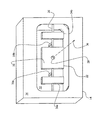
本発明の第一の好ましい実施形態による、光ファイバ8と共に用いられる光走査デバイス全体が、図1A中の2で示されている。光走査デバイス2は、走査素子14、透明プレート18上に支持されている固定されている平面ミラー16、及び集光レンズ20を含む。
The entire optical scanning device used with the
走査素子14は、固定ミラー16の反射表面に対向する反射表面を有する平面のピボットミラー(pivotable mirror)22を含む。ピボットミラー22は、その両端に、片側に一つずつ、対をなす平衡素子(counterbalancing element)24a、24bからなる釣合いおもりが配置されている。ピボットミラー22と平衡素子24a、24bは、シリコントーションバー26上に備えつけられている。
The
ピボットミラー22は、光ファイバ8の先端30位置に、中央円形開口部28を有し、その結果、光ファイバ8から放出される光は妨げられることなくピボットミラー22に形成された開口部28を通過することができる。従って、円形開口部28の直径は、光ファイバ8の直径よりも大きくなっており、中央の開口部28は出射光または戻り光に対して空間的なフィルタのように作用することはない。同様に、戻り光はピボットミラー22の開口部28を通過後、光ファイバ8の先端30によって受光され得る。
The
使用時には、一般的にレーザ光源である適切な光源(図示していない)からの光は、光ファイバ8に沿って先端30の方へ伝えられ、先端30からピボットミラー22の円形の中央開口部28を通って固定ミラー16の方へと射出される。この光は、固定ミラー16からピボットミラー22へ反射され、ピボットミラー22によって集光レンズ20の方へ反射される。このプロセスでは、後に説明するように、固定ミラー16から中央開口部28へと戻る反射その他によりいくらかの光が失われる。
In use, light from a suitable light source (not shown), typically a laser light source, is transmitted along the
集光レンズ20に到達する光は、試料(sample)が置かれる点18に向かって集光される。同様に、その試料によって返される光は(反射光であろうと蛍光であろうと)、集光レンズ20によって集められ、光ファイバ8の先端30に向かって同一の光経路に沿って戻される。適切なビーム分岐技術によって、その後、この戻り光(もしくはその一部)を、検出器(図示していない)へと導くことができる。
The light reaching the
図1Aには示されていないが、走査素子14は、振動の形式でトーションバー26回りにピボットミラー22を軸回転させるための静電駆動装置を含み、その結果、ピボットミラー22から反射される光は、(図1Aに示される視野で)図の紙面の奥と手前の方向に走査される。平衡素子24a、24bも軸回転されるが、ピボットミラー22の動きに対し180°位相をずらし、その結果として平衡効果を提供する。
Although not shown in FIG. 1A, the
光走査デバイス2の変形例(これも光ファイバ8と共に用いられる)全体を、図1B中に4で示す。走査デバイス4は、大部分の点で図1Aの走査デバイス2と同一であるが、戻り光を90°進路変更して戻りファイバ12(図示されていない適切な光検出器に接続されている)の方へ向けるためのビームスプリッタ10を含む。
An overall variation of the optical scanning device 2 (also used with the optical fiber 8) is indicated by 4 in FIG. 1B. The scanning device 4 is in most respects identical to the
光走査デバイス2の別の変形例を、(これも光ファイバ8と共に用いられる)全体を、図1C中に6で示す。この変形例では、光ファイバ8の先端30が、走査デバイス6の中央開口部28の内部に(あるいは、任意で、そのわずかに前に)位置されている。この変形例では、中央開口部28は、図1Aや図1Bに示される変形例中の開口部28よりもわずかに大きな直径を有し、その結果として、ミラー22が使用中に回動しているときを含むミラー22の動きを妨害することなくファイバ8を収容することができる。
Another variation of the
さらに、走査デバイス2の他の変形例では、第二の(戻り)ファイバが光ファイバ8に隣接して配置され、走査デバイス2は、試料から戻ってくる光を少量だけ分岐させるために、走査素子14とプレート18の間またはプレート18と集光レンズ20の間のどちらかに配置される付加的な光素子を含む。したがって、この戻り光は、ファイバ8よりもむしろ第二ファイバによって集められ、その結果、戻り光をファイバ8から取り出し、検出器の方に導くためのビームスプリッタが必要なくなる。
Furthermore, in another variant of the
図2に走査素子14をより詳細に示す。また、走査素子14のフレーム34の後部壁32からミラー22と平衡素子24a、24bとのそれぞれの間に配置されているトーションバー26へと伸びているシリコン製のマイクロ組み立て支持柱30a、30bもこの図において見ることができる。支持柱30a、30bは、ミラー22と平衡素子24a、24bの動作によってトーションバー26に波動が誘発されること防ぐために設けられている。
FIG. 2 shows the
光ファイバ8からの光(図示されていない)は、中央開口部28を通って方向36へ射出される。
Light from the optical fiber 8 (not shown) exits in the
電磁駆動装置は、米国特許No. 6,057,952やNo. 6,172,789により教示されるものを含む、どのような適切な形状であってもよい。その場合、ミラー22の反射面38は、電極としてまたは反射体としての両方として作用する、導電性且つ反射性の物質を塗布したものであってもよい。
The electromagnetic drive may be of any suitable shape, including those taught by US Pat. Nos. 6,057,952 and No. 6,172,789. In that case, the reflecting
他の適切な、代替的な駆動装置は、WO 99/04301に開示されている駆動装置に相当する、電磁駆動装置を含む。 Other suitable alternative drive devices include electromagnetic drive devices, corresponding to the drive devices disclosed in WO 99/04301.
上述のように、平衡素子24a、24bは、ミラー22と正確につりあい、フレーム34へ伝わりそこから光学ヘッドが含むデバイス2の全体へと伝わる反偶力の連結を最小にするように設計されている。平衡素子24a、24bは、少なくとも2つの方法で、ミラー22と位相をずらして駆動可能である。第一の方法として、それら平衡素子は、ミラー22を駆動する静電駆動装置により、ただしミラー22と位相をずらして駆動可能である。もう一つの方法として、静電駆動装置を、ミラー22を駆動し、さらにトーションバー26を介したミラー22と平衡素子24a、24bとの機械的接合を通じて、平衡素子24a、24bを駆動するために使用することができる。しかしながら、どちらのケースにおいても、駆動装置は、ミラー22と平衡素子24a、24bの両者を駆動する。
As mentioned above, the
当業者には明らかなように、ミラー22と平衡素子24a、24bは、共鳴振動動作(resonant oscillatory motion)で駆動される。そのシステムは、高いQ値を有し、その結果、振動を維持するためには最小のエネルギーを入力すれば良い。走査デバイス2はロックインセンサ(図示されていない)を備え、ロックインセンサは、駆動装置との協働により、ミラー22と平衡素子24a、24bが共鳴振動数で駆動され維持されることを可能にしている。
As will be apparent to those skilled in the art, the
走査デバイス2は、ミラー22が減圧雰囲気中に収容されるように、ケースまたは光学ヘッド(図示されていない)の中に構成されている。この構成は、ミラー22と平衡素子24a、24bの動作に対する大気雰囲気の抵抗を減少させるが、もっと一般的には、密閉された光学ヘッドがその内部に収容している素子の湿気、油分、及び埃からの汚染に対する脆弱さを減少させている。実際には、実施形態の一つでは、透明なシールが集光レンズ20を覆っており、集光レンズ20により提供される焦点合わせ光学系にダメージを与える危険性なしに、このシールの汚染を取り除くことができる。
The
図3Aは、走査素子14の断面図であり、その内部には、ミラー22、平衡素子24a、24b、トーションバー26、支持柱30a、30b、及び光ファイバ8が見られる。この図から明らかなように、光ファイバ8は、走査素子14のフレーム34の後壁32内の開口部40の内部に固定されている。開口部40は、ミラー22の中央開口部28に位置合わせさせている。任意で、光ファイバ8は、必要であれば、例えば中央開口部28の方へ後壁32から伸びるつばのようなもので、付加的に支持されていてもよい。光ファイバ8は、ミラー22の回転動作を妨害しないようにしつつ、可能な限り中央開口部28の方へ長く伸ばされている。
FIG. 3A is a cross-sectional view of the
図3Bは、図3Aと似ているが、図1Cに示された変形例による走査素子14、すなわち、ファイバ8を収容するために幾分大きな中央開口部28を有するものを示している。
FIG. 3B shows a
図4を参照すると、本発明の第二の好ましい実施形態によれば、走査素子は実質的には図2に示される素子と同一であるが、基本的に円形のミラー122と、ミラー122を囲むように配置され、ミラー122と同心である環状の素子からなる単一の平衡素子124という形態を取った釣合いおもりを有する。
Referring to FIG. 4, according to a second preferred embodiment of the present invention, the scanning element is substantially the same as the element shown in FIG. It has a counterweight in the form of a
この構成は多くの利点を持っている。平衡素子124はミラー122を囲んでいるので、ミラー122自身と比較して、トーションバー126からより離れた位置に質量の大部分を有する。結果として、平衡素子124の慣性モーメントは、図1から3の平衡素子24a、24bの慣性モーメントと比較して、その質量に対し比較的大きい。従って、より小さい質量ながら同程度の平衡状態を平衡素子124によって提供することができ、その結果、走査素子全体を小型軽量化することができる。
This configuration has many advantages. Since the
また、この実施形態では、シリコンマイクロ組み立て支持柱を、ミラー122と平衡素子124の間のトーションバー126の背後(図4を上から見て)に備えてもよい。
Also, in this embodiment, a silicon microassembly support post may be provided behind the
また、第二実施形態の走査素子は、さらに、図4に概略的に示される静電駆動装置を備えている。静電駆動装置は、電極144a、144bにそれぞれ接続され、且つ、以下に説明する方法でミラー122と平衡素子124に取り付けられた、2つの交流電源142a、142bを含む。
Further, the scanning element of the second embodiment further includes an electrostatic driving device schematically shown in FIG. The electrostatic drive includes two
電極144aは、電源142aから延びており、トーションバー126に沿って平衡素子124へと至り、その後、再びトーションバー126に到達するまでほぼ半円形状で平衡素子124を回って進み、トーションバー126の次にミラー22へと進み、トーションバー126に到達するまで平衡素子124を回る経路から遠く離れたほぼ半円形状でミラー122の周縁部周りを通る。その結果、電源142aを用いて、平衡素子124の上部(図4において)とミラー122の下部を同時に帯電させることができる。
The
電源142bの電極144bは相補的な型で配置され、その結果、平衡素子124の下部(図4において)とミラー122の上部を電源142bによって同時に帯電させることができる。
The
使用時は、電源142aと電源142bの出力は、位相が180°ずれている。電源142aの出力は、本質的には、負の最大の値とゼロとの間の正弦関数であり、一方、電源142bの出力は正であって、(より小さい)正の最大の値とゼロとの間の正弦関数である。
In use, the outputs of the
参照電極(図示されていない)が、この実施形態の素子のフレーム(図示されていない)の内部、ミラー122と平衡素子124の背後に備えられており、参照電極は、+Veまたは−Veのどちらか一方に帯電して維持されている。
A reference electrode (not shown) is provided inside the element frame (not shown) of this embodiment, behind the
電源142a、142bが、それぞれの電極144a、144b及び接地電極間に、位相が180°ずれた上述の電圧を印加するとき、接地電極と電極144a、144bの間に結果として生じる静電気力は、反偶力が最小となるように、ミラー122と平衡素子124を、同時に180°位相がずれた状態で、トーションバー126の回りに回転振動させる。
When the
図5は、本発明の第三の実施形態の走査素子214の分解概略図である。走査素子214は、トーションバー226に回動可能に装着されたミラー222を含む前フレーム234を含む。ミラー222は、円形の中央開口部228を含む。光ファイバ208は、その射出端230を中央開口部228の背後(図5において)に配置し、中央開口部228に位置合わせされている。
FIG. 5 is an exploded schematic view of the
ミラー222は、静電駆動装置または電磁駆動装置(上記参照)により、振動する方法または揺動する方法で駆動される。
The
また、走査素子214は、4つのコーナー柱252により前フレーム234に機械的に接続されている後フレーム250を含む。
The
後フレーム250は、大部分が、前フレーム234と同様である。しかしながら、ピボットミラーを有する代わりに、後フレーム250がトーションバー上に備えられた同様に配置されたピボット円形釣合いおもりを含む。また、走査素子214は、後フレーム250の釣合いおもり素子がミラー222と位相が180°ずれて駆動されるように構成されている。
The
それらのピボット素子(すなわち、ミラー250及び釣合いおもり)の構成は、図6の部分断面図にさらにはっきりと示されており、図中ではピボットミラー222の背後に位置するピボット釣合いおもり254が見られる。釣合いおもり254は、ミラー222の中央開口部228と同軸である、円形の中央開口部256を有する。光ファイバ208が、単にミラー222の中央開口部228の後方までで終わる一方で、釣合いおもり254の中央開口部256を貫通しているので、釣合いおもり254の中央開口部256はミラー222の中央開口部228よりも大きな直径を有する。釣合いおもり254の中央開口部256は、釣合いおもり254が、必要に応じて、光ファイバ208に接触することなく回転できるよう、十分に大きな直径を有する。
The configuration of these pivot elements (ie, the
図6と類似の側断面図である図7を参照すると、使用時には、ミラー222と釣合いおもり254は、他の構成要素への反偶力の伝達を最小にするために、位相を180°ずらして駆動される。
Referring to FIG. 7, which is a side cross-sectional view similar to FIG. 6, in use, the
この実施形態では、走査素子214は、好ましくは、図4に示される静電駆動装置に相当する静電駆動装置であり、ミラー222と釣合いおもり250の間に接地電極が配置されるものを有する。これらの電極の配置は、適宜調整される。
In this embodiment, the
上述の実施形態の各々においては、釣合いおもり(一つもしくは多くの平衡素子を含む)を製造するための好ましい技術は、できる限り綿密にミラーの平衡を保つように、以下の段階を含む。 In each of the above-described embodiments, a preferred technique for manufacturing a counterweight (including one or many balancing elements) includes the following steps so as to balance the mirror as closely as possible.
釣合いおもりは最初に必要よりも重く作られ、ミラーと正確に平衡することがわかるまで、釣合いおもりの連続的なレーザーアブレーションによって調整される。これは、3つのピエゾセンサ上に走査素子を備え付け、ピエゾセンサからの信号を測定すると同時に走査素子を駆動することによって把握される。その結果、走査素子中の反偶力をピエゾセンサによって検出することができ、ピエゾセンサからの検出出力がなくなる(あるいは、無視できる)まで、釣合いおもりは連続的にレーザで削り取られる。 The counterweight is initially made heavier than necessary and is adjusted by continuous laser ablation of the counterweight until it is found to be accurately balanced with the mirror. This can be grasped by providing scanning elements on the three piezoelectric sensors and measuring the signals from the piezoelectric sensors and simultaneously driving the scanning elements. As a result, the counter-couple force in the scanning element can be detected by the piezo sensor, and the counterweight is continuously scraped by the laser until the detection output from the piezo sensor disappears (or can be ignored).
また、最終的な、好適な操作状態をより正確にシミュレートするために、この調整過程を減圧雰囲気中で行うこともできる。 This adjustment process can also be carried out in a reduced pressure atmosphere in order to more accurately simulate the final preferred operating conditions.
釣合いおもりが金属の場合、容易に削り取ることのできるコーティングを施し、調整は釣合いおもりそれ自身よりはむしろそのコーティングに対するレーザーアブレーションによることができる。代替的には、そのような実施形態では、ミラーまたは他の釣合いおもり素子にそのコーティングを施し、そのコーティングを削り取るようにすることができる。 If the counterweight is metal, a coating that can be easily scraped off is applied and adjustment can be by laser ablation of the coating rather than the counterweight itself. Alternatively, in such embodiments, a mirror or other counterweight element can be applied with the coating and the coating can be scraped off.
本発明の思想と範囲内での変形が、本技術の分野における通常の知識を有する者により容易に達成され得、したがって、この発明は以上に例示された特定の実施形態に制限されるものではない。 Variations within the spirit and scope of the present invention can be readily accomplished by those having ordinary skill in the art and, therefore, the invention is not limited to the specific embodiments illustrated above. Absent.
さらに、本明細書に記載したいかなる従来技術の参照も、その従来技術の参照が通常の一般的知識の一部を形成する、或いは形成していたことを意味することを意図したものではない。
Furthermore, any prior art reference set forth herein is not intended to imply that that prior art reference formed or formed part of ordinary general knowledge.
2 光走査デバイス
4 光走査デバイス
8 光ファイバ
10 ビームスプリッタ
12 戻り光ファイバ
14 走査素子
16 固定平面ミラー
18 透明プレート
20 集光レンズ
22 ピボットミラー
24a、24b 平衡素子
26 トーションバー
28 開口部
30 先端
30a、30b 支持柱
32 後壁
34 フレーム
40 開口部
122 円形ミラー
124 平衡素子
126 トーションバー
128 開口部
142a、142b 交流電源
144a、144b 電極
208 光ファイバ
214 走査素子
222 ミラー
226 トーションバー
228 開口部
230 射出端
234 前フレーム
250 後フレーム
252 コーナー柱
254 釣合いおもり
256 開口部
2 Optical scanning device 4
Claims (21)
前記光源からの光を受けるための回動可能に取り付けられたミラー;
カウンターバランス;及び
反偶力を減少させるために前記ミラーと前記カウンターバランスを反対方向に同時に回動振動させるための駆動装置、を有する前記光走査デバイス。 An optical scanning device for scanning light from a light source,
A pivotally mounted mirror for receiving light from the light source;
The optical scanning device comprising: a counterbalance; and a driving device for simultaneously rotating and vibrating the mirror and the counterbalance in opposite directions to reduce the counter-couple force.
ミラーから前記光を反射し;
前記ミラーを回動振動させて前記ミラーから反射された前記光を走査するように前記ミラーを駆動し;及び
前記ミラーに対するカウンターバランスとして作用するカウンターバランスを駆動し;
前記ミラーの前記回動による反偶力が、前記カウンターバランスによって減少する、ことを含む方法。 A method of scanning light,
Reflecting the light from a mirror;
Driving the mirror to rotate and vibrate the mirror to scan the light reflected from the mirror; and driving a counterbalance that acts as a counterbalance to the mirror;
The counter-couple force due to the rotation of the mirror is reduced by the counterbalance.
1次元以上の前記デバイスの振動を検出するための一つ以上のセンサ上に前記ミラーとカウンターバランスを取り付けること;
前記デバイスを操作し、前記センサを用いて前記デバイス中のいかなる振動をも監視すること;及び
前記デバイス中のいかなる振動をも減少させるように前記デバイスを調整すること、を含む方法。 A method of balancing an optical scanning device according to any of claims 1 to 13, comprising
Mounting the mirror and counterbalance on one or more sensors for detecting vibrations of the device in one or more dimensions;
Manipulating the device and monitoring any vibrations in the device using the sensor; and adjusting the device to reduce any vibrations in the device.
21. A method according to claim 19 or claim 20, wherein the removing is performed in a reduced pressure atmosphere.
Applications Claiming Priority (2)
| Application Number | Priority Date | Filing Date | Title |
|---|---|---|---|
| US36727002P | 2002-03-26 | 2002-03-26 | |
| PCT/AU2003/000379 WO2003081318A1 (en) | 2002-03-26 | 2003-03-26 | Light scanning device |
Publications (2)
| Publication Number | Publication Date |
|---|---|
| JP2005521098A true JP2005521098A (en) | 2005-07-14 |
| JP2005521098A5 JP2005521098A5 (en) | 2006-05-18 |
Family
ID=28454845
Family Applications (1)
| Application Number | Title | Priority Date | Filing Date |
|---|---|---|---|
| JP2003578994A Pending JP2005521098A (en) | 2002-03-26 | 2003-03-26 | Optical scanning device |
Country Status (5)
| Country | Link |
|---|---|
| US (1) | US7248390B2 (en) |
| JP (1) | JP2005521098A (en) |
| AU (1) | AU2003215417A1 (en) |
| DE (1) | DE10392442T8 (en) |
| WO (1) | WO2003081318A1 (en) |
Cited By (3)
| Publication number | Priority date | Publication date | Assignee | Title |
|---|---|---|---|---|
| JP2008254162A (en) * | 2006-06-07 | 2008-10-23 | Canon Inc | Oscillator device, optical deflector and optical instrument using the same |
| JP2009501960A (en) * | 2005-07-21 | 2009-01-22 | ユニバーシティ・オブ・ワシントン | Method and system for balancing scanning beam devices |
| JPWO2017149713A1 (en) * | 2016-03-03 | 2019-02-07 | 北陽電機株式会社 | Optical deflection device |
Families Citing this family (9)
| Publication number | Priority date | Publication date | Assignee | Title |
|---|---|---|---|---|
| JP4262574B2 (en) * | 2003-10-30 | 2009-05-13 | オリンパス株式会社 | Optical deflector |
| US7395967B2 (en) * | 2005-07-21 | 2008-07-08 | University Of Washington | Methods and systems for counterbalancing a scanning beam device |
| US8854442B2 (en) * | 2006-02-10 | 2014-10-07 | Freedom Scientific, Inc. | Retainer for electronic magnification device |
| US7929013B2 (en) | 2006-02-10 | 2011-04-19 | Freedom Scientific, Inc. | Desktop electronic magnifier |
| US8854441B2 (en) * | 2006-02-10 | 2014-10-07 | Freedom Scientific, Inc. | Electronic magnification device |
| US7557972B2 (en) * | 2006-06-07 | 2009-07-07 | Canon Kabushiki Kaisha | Oscillator device, optical deflector and optical instrument using the same |
| JP5064864B2 (en) * | 2007-04-02 | 2012-10-31 | キヤノン株式会社 | Optical deflection apparatus, image forming apparatus, and driving method of optical deflection apparatus |
| JP5065116B2 (en) * | 2007-06-14 | 2012-10-31 | キヤノン株式会社 | Oscillator device, optical deflection device, and control method thereof |
| US9595757B2 (en) | 2013-12-24 | 2017-03-14 | The Boeing Company | Integral RF-optical phased array module |
Family Cites Families (11)
| Publication number | Priority date | Publication date | Assignee | Title |
|---|---|---|---|---|
| US3952217A (en) * | 1973-09-25 | 1976-04-20 | The Perkin-Elmer Corporation | Drive for scanning mirror |
| GB1457995A (en) * | 1975-05-23 | 1976-12-08 | Perkin Elmer Corp | Scanning element assembly |
| US4902083A (en) | 1988-05-31 | 1990-02-20 | Reflection Technology, Inc. | Low vibration resonant scanning unit for miniature optical display apparatus |
| DE4001242A1 (en) * | 1990-01-18 | 1991-07-25 | Telefunken Systemtechnik | Linear optical scanner for missile - has mirror on oscillating segmental rotor with lateral return springs and located between two compensatory rotors |
| US5210636A (en) * | 1991-07-19 | 1993-05-11 | Baer Stephen C | Rotational oscillatory optical scanning device |
| AUPO790197A0 (en) | 1997-07-16 | 1997-08-07 | Optiscan Pty Limited | Scanning microscope with miniature head |
| JP4414498B2 (en) * | 1997-12-09 | 2010-02-10 | オリンパス株式会社 | Optical deflector |
| US5995264A (en) | 1998-01-20 | 1999-11-30 | University Of Washington | Counter balanced optical scanner |
| US6107770A (en) | 1998-01-27 | 2000-08-22 | Lockheed Martin Corporation | Control system for counter-oscillating masses |
| US6172789B1 (en) * | 1999-01-14 | 2001-01-09 | The Board Of Trustees Of The Leland Stanford Junior University | Light scanning device and confocal optical device using the same |
| US6057952A (en) | 1999-01-14 | 2000-05-02 | Olympus Optical Co., Ltd. | Light scanning device and confocal optical device using the same |
-
2003
- 2003-03-26 DE DE2003192442 patent/DE10392442T8/en active Active
- 2003-03-26 AU AU2003215417A patent/AU2003215417A1/en not_active Abandoned
- 2003-03-26 JP JP2003578994A patent/JP2005521098A/en active Pending
- 2003-03-26 US US10/508,541 patent/US7248390B2/en not_active Expired - Lifetime
- 2003-03-26 WO PCT/AU2003/000379 patent/WO2003081318A1/en active Application Filing
Cited By (3)
| Publication number | Priority date | Publication date | Assignee | Title |
|---|---|---|---|---|
| JP2009501960A (en) * | 2005-07-21 | 2009-01-22 | ユニバーシティ・オブ・ワシントン | Method and system for balancing scanning beam devices |
| JP2008254162A (en) * | 2006-06-07 | 2008-10-23 | Canon Inc | Oscillator device, optical deflector and optical instrument using the same |
| JPWO2017149713A1 (en) * | 2016-03-03 | 2019-02-07 | 北陽電機株式会社 | Optical deflection device |
Also Published As
| Publication number | Publication date |
|---|---|
| WO2003081318A1 (en) | 2003-10-02 |
| AU2003215417A1 (en) | 2003-10-08 |
| US7248390B2 (en) | 2007-07-24 |
| DE10392442T5 (en) | 2005-04-07 |
| DE10392442T8 (en) | 2005-07-14 |
| US20050162722A1 (en) | 2005-07-28 |
Similar Documents
| Publication | Publication Date | Title |
|---|---|---|
| JP2005521098A (en) | Optical scanning device | |
| KR0181724B1 (en) | Fiber optic ribbon subminiature display for head/helmet mounted display | |
| US8294968B2 (en) | Optical scanning element, driving method for same, and optical scanning probe employing optical scanning element | |
| US5742419A (en) | Miniature scanning confocal microscope | |
| US7983739B2 (en) | Position tracking and control for a scanning assembly | |
| JP6086674B2 (en) | Optical scanning device | |
| JP2010286477A (en) | Gyroscope and rotation detection method | |
| JPH0738208B2 (en) | Mirrorless scanner with movable laser element, optical element and sensor element | |
| US10914939B2 (en) | MEMS reflector system | |
| JP2008040240A (en) | Light deflector and its manufacturing method | |
| JP2010117442A (en) | Fiber-optic scanning endoscope, fiber-optic scanning endoscope processor, and fiber-optic scanning endoscope device | |
| US8879135B2 (en) | Device and method for deflecting a light beam in two different directions and scanning microscope | |
| US8626468B2 (en) | MEMS device comprising oscillations measurements means | |
| JP2005521098A5 (en) | ||
| JP3861357B2 (en) | Microscope revolver and microscope integrated with optical device | |
| JP6987493B2 (en) | microscope | |
| CN107870416B (en) | Optical scanning device | |
| JP6945533B2 (en) | A scanning device that scans an object for use in a scanning microscope. | |
| JP2012226020A (en) | Distance measuring instrument | |
| JP2004504617A (en) | Confocal imaging system with segmented retroreflector | |
| US20030214707A1 (en) | Scanning microscope and beam deflection device | |
| JP2000292735A (en) | Optical scanner | |
| JPH11211990A (en) | Total reflection lighting type microscope device and sample stage | |
| JPH11337860A (en) | Optical scanner | |
| JP2613130B2 (en) | Confocal scanning phase contrast microscope |
Legal Events
| Date | Code | Title | Description |
|---|---|---|---|
| A621 | Written request for application examination |
Free format text: JAPANESE INTERMEDIATE CODE: A621 Effective date: 20051104 |
|
| A521 | Request for written amendment filed |
Free format text: JAPANESE INTERMEDIATE CODE: A523 Effective date: 20060324 |
|
| A711 | Notification of change in applicant |
Free format text: JAPANESE INTERMEDIATE CODE: A712 Effective date: 20080501 |
|
| A131 | Notification of reasons for refusal |
Free format text: JAPANESE INTERMEDIATE CODE: A131 Effective date: 20081107 |
|
| A601 | Written request for extension of time |
Free format text: JAPANESE INTERMEDIATE CODE: A601 Effective date: 20090209 |
|
| A602 | Written permission of extension of time |
Free format text: JAPANESE INTERMEDIATE CODE: A602 Effective date: 20090217 |
|
| A601 | Written request for extension of time |
Free format text: JAPANESE INTERMEDIATE CODE: A601 Effective date: 20090306 |
|
| A521 | Request for written amendment filed |
Free format text: JAPANESE INTERMEDIATE CODE: A523 Effective date: 20090309 |
|
| A602 | Written permission of extension of time |
Free format text: JAPANESE INTERMEDIATE CODE: A602 Effective date: 20090313 |
|
| A02 | Decision of refusal |
Free format text: JAPANESE INTERMEDIATE CODE: A02 Effective date: 20090520 |