JP2005501286A - Optical coat product and manufacturing method thereof - Google Patents
Optical coat product and manufacturing method thereof Download PDFInfo
- Publication number
- JP2005501286A JP2005501286A JP2003524053A JP2003524053A JP2005501286A JP 2005501286 A JP2005501286 A JP 2005501286A JP 2003524053 A JP2003524053 A JP 2003524053A JP 2003524053 A JP2003524053 A JP 2003524053A JP 2005501286 A JP2005501286 A JP 2005501286A
- Authority
- JP
- Japan
- Prior art keywords
- layers
- product
- substrate
- optical
- layer
- Prior art date
- Legal status (The legal status is an assumption and is not a legal conclusion. Google has not performed a legal analysis and makes no representation as to the accuracy of the status listed.)
- Pending
Links
Images


Classifications
-
- C—CHEMISTRY; METALLURGY
- C23—COATING METALLIC MATERIAL; COATING MATERIAL WITH METALLIC MATERIAL; CHEMICAL SURFACE TREATMENT; DIFFUSION TREATMENT OF METALLIC MATERIAL; COATING BY VACUUM EVAPORATION, BY SPUTTERING, BY ION IMPLANTATION OR BY CHEMICAL VAPOUR DEPOSITION, IN GENERAL; INHIBITING CORROSION OF METALLIC MATERIAL OR INCRUSTATION IN GENERAL
- C23C—COATING METALLIC MATERIAL; COATING MATERIAL WITH METALLIC MATERIAL; SURFACE TREATMENT OF METALLIC MATERIAL BY DIFFUSION INTO THE SURFACE, BY CHEMICAL CONVERSION OR SUBSTITUTION; COATING BY VACUUM EVAPORATION, BY SPUTTERING, BY ION IMPLANTATION OR BY CHEMICAL VAPOUR DEPOSITION, IN GENERAL
- C23C16/00—Chemical coating by decomposition of gaseous compounds, without leaving reaction products of surface material in the coating, i.e. chemical vapour deposition [CVD] processes
- C23C16/22—Chemical coating by decomposition of gaseous compounds, without leaving reaction products of surface material in the coating, i.e. chemical vapour deposition [CVD] processes characterised by the deposition of inorganic material, other than metallic material
- C23C16/24—Deposition of silicon only
-
- C—CHEMISTRY; METALLURGY
- C23—COATING METALLIC MATERIAL; COATING MATERIAL WITH METALLIC MATERIAL; CHEMICAL SURFACE TREATMENT; DIFFUSION TREATMENT OF METALLIC MATERIAL; COATING BY VACUUM EVAPORATION, BY SPUTTERING, BY ION IMPLANTATION OR BY CHEMICAL VAPOUR DEPOSITION, IN GENERAL; INHIBITING CORROSION OF METALLIC MATERIAL OR INCRUSTATION IN GENERAL
- C23C—COATING METALLIC MATERIAL; COATING MATERIAL WITH METALLIC MATERIAL; SURFACE TREATMENT OF METALLIC MATERIAL BY DIFFUSION INTO THE SURFACE, BY CHEMICAL CONVERSION OR SUBSTITUTION; COATING BY VACUUM EVAPORATION, BY SPUTTERING, BY ION IMPLANTATION OR BY CHEMICAL VAPOUR DEPOSITION, IN GENERAL
- C23C16/00—Chemical coating by decomposition of gaseous compounds, without leaving reaction products of surface material in the coating, i.e. chemical vapour deposition [CVD] processes
- C23C16/22—Chemical coating by decomposition of gaseous compounds, without leaving reaction products of surface material in the coating, i.e. chemical vapour deposition [CVD] processes characterised by the deposition of inorganic material, other than metallic material
- C23C16/30—Deposition of compounds, mixtures or solid solutions, e.g. borides, carbides, nitrides
- C23C16/40—Oxides
- C23C16/401—Oxides containing silicon
- C23C16/402—Silicon dioxide
-
- G—PHYSICS
- G02—OPTICS
- G02B—OPTICAL ELEMENTS, SYSTEMS OR APPARATUS
- G02B1/00—Optical elements characterised by the material of which they are made; Optical coatings for optical elements
- G02B1/10—Optical coatings produced by application to, or surface treatment of, optical elements
- G02B1/11—Anti-reflection coatings
- G02B1/113—Anti-reflection coatings using inorganic layer materials only
- G02B1/115—Multilayers
-
- Y—GENERAL TAGGING OF NEW TECHNOLOGICAL DEVELOPMENTS; GENERAL TAGGING OF CROSS-SECTIONAL TECHNOLOGIES SPANNING OVER SEVERAL SECTIONS OF THE IPC; TECHNICAL SUBJECTS COVERED BY FORMER USPC CROSS-REFERENCE ART COLLECTIONS [XRACs] AND DIGESTS
- Y10—TECHNICAL SUBJECTS COVERED BY FORMER USPC
- Y10T—TECHNICAL SUBJECTS COVERED BY FORMER US CLASSIFICATION
- Y10T428/00—Stock material or miscellaneous articles
- Y10T428/26—Web or sheet containing structurally defined element or component, the element or component having a specified physical dimension
-
- Y—GENERAL TAGGING OF NEW TECHNOLOGICAL DEVELOPMENTS; GENERAL TAGGING OF CROSS-SECTIONAL TECHNOLOGIES SPANNING OVER SEVERAL SECTIONS OF THE IPC; TECHNICAL SUBJECTS COVERED BY FORMER USPC CROSS-REFERENCE ART COLLECTIONS [XRACs] AND DIGESTS
- Y10—TECHNICAL SUBJECTS COVERED BY FORMER USPC
- Y10T—TECHNICAL SUBJECTS COVERED BY FORMER US CLASSIFICATION
- Y10T428/00—Stock material or miscellaneous articles
- Y10T428/31504—Composite [nonstructural laminate]
- Y10T428/31507—Of polycarbonate
-
- Y—GENERAL TAGGING OF NEW TECHNOLOGICAL DEVELOPMENTS; GENERAL TAGGING OF CROSS-SECTIONAL TECHNOLOGIES SPANNING OVER SEVERAL SECTIONS OF THE IPC; TECHNICAL SUBJECTS COVERED BY FORMER USPC CROSS-REFERENCE ART COLLECTIONS [XRACs] AND DIGESTS
- Y10—TECHNICAL SUBJECTS COVERED BY FORMER USPC
- Y10T—TECHNICAL SUBJECTS COVERED BY FORMER US CLASSIFICATION
- Y10T428/00—Stock material or miscellaneous articles
- Y10T428/31504—Composite [nonstructural laminate]
- Y10T428/31511—Of epoxy ether
-
- Y—GENERAL TAGGING OF NEW TECHNOLOGICAL DEVELOPMENTS; GENERAL TAGGING OF CROSS-SECTIONAL TECHNOLOGIES SPANNING OVER SEVERAL SECTIONS OF THE IPC; TECHNICAL SUBJECTS COVERED BY FORMER USPC CROSS-REFERENCE ART COLLECTIONS [XRACs] AND DIGESTS
- Y10—TECHNICAL SUBJECTS COVERED BY FORMER USPC
- Y10T—TECHNICAL SUBJECTS COVERED BY FORMER US CLASSIFICATION
- Y10T428/00—Stock material or miscellaneous articles
- Y10T428/31504—Composite [nonstructural laminate]
- Y10T428/31652—Of asbestos
- Y10T428/31667—Next to addition polymer from unsaturated monomers, or aldehyde or ketone condensation product
Abstract
【課題】光学性能の温度変化が低減した光学製品の提供。
【解決手段】オプティカルコート製品(400)は、ポリマー基板(420)と複数の光学的コーティング層とを備え、コーティング層はプラズマCVDで交互に堆積した二酸化ケイ素層(460)と非晶質水素化ケイ素層(440)とを含む。製品(400)は広い温度域でほぼ一定な光学的特性を有する。適当なポリマー基板には、ポリメチルメタクリレート又は芳香族ポリカーボネートがある。
【選択図】図4An optical product with reduced temperature change in optical performance is provided.
An optical coat product (400) comprises a polymer substrate (420) and a plurality of optical coating layers, wherein the coating layers and silicon dioxide layers (460) alternately deposited by plasma CVD and amorphous hydrogenation. A silicon layer (440). The product (400) has almost constant optical properties over a wide temperature range. Suitable polymer substrates include polymethyl methacrylate or aromatic polycarbonate.
[Selection] Figure 4
Description
【技術分野】
【0001】
本発明は、オプティカルコーティングを有する製品及びその製造方法に関する。さらに具体的には、本発明は熱に安定な光学レスポンスを示すオプティカルコート製品に関する。
【背景技術】
【0002】
オプティカルコート製品は、熱光学スイッチなどの用途における干渉フィルターとして有用である。オプティカルコート製品は概して多数のコーティング層を有する基板からなり、基板とコーティング層は様々なスペクトル域(典型的には可視及び/又は短波長赤外域)の光に透明であり、コーティング層は高い屈折率と低い屈折率とを交互に有する。「短波長赤外」という用語は約700〜2500nmの領域をいう。コーティング系の基本的特徴は、隣り合ったコーティング層の屈折率にかなりの差があることであり、典型的には約1.5以上の屈折率比(以下、「R」と略す。)で表される。この比が高いのが望ましいことが多い。
【0003】
当技術分野で公知の典型的なオプティカルコート製品は、ガラス基板上に酸化ケイ素(SiO2)コーティングと酸化タンタル(Ta2O5)又は二酸化チタン(TiO2)コーティングとが交互に設けられている。かかる製品のコーティング系はそれぞれ1.5又は1.6のR値を有する。
【0004】
コーティング系のR値が高い(例えば2.0超)光学製品を製造できれば望ましい。かかる値は、フューズドシリカ(すなわちガラス)基板上の二酸化ケイ素と非晶質水素化ケイ素(以下、「a−Si:H」という。)の交互コーティングを用いることで得ることができる。コーティングは、プラズマ化学気相堆積法(以下、「PECVD」という。)で好適に堆積し得る。46層のコーティング層からなる合計厚さ約7.5μmのSiO2/a−SiHコーティング系が、64層からなる厚さ13μmのSiO2−Ta2O5コーティング系と同じ光学的挙動を示すことが判明した。
【0005】
光学製品の光学レスポンスは、そのコーティングの屈折率及び厚さに依存する。これらの特性はいずれも温度の関数である。熱光学係数は温度の関数としての材料の屈折率の変化を表し、熱膨張係数(以下、「CTE」という。)としても知られる熱機械係数は、温度による物理的寸法の変化を表す。
【0006】
ガラスをSiO2層とa−SiH層で交互にコーティングすると、基板のCTEとコーティングのCTE及び熱光学係数によって、温度に伴って光学的挙動に重大な変化が生じる。この変化の主要因子はa−SiH層の比較的高い熱光学係数である。そこで、加熱すると、干渉構造のシフト(普通は反射光の半値全幅(FWHM)間の中心波長による)が認められる。このシフトは典型的には75℃の温度変化で7nm程度である。上述のように、基板のCTEを用いてコーティングの光学シフトを補償することができる場合もある。
【0007】
ガラスのCTEは7.8ppm/℃程度である。基板のCTEが66ppm/℃に可及的に近くなるように基板を選択すると、基板のCTEがコーティングの効果をほぼ相殺するので、光学的挙動への温度効果(例えば上述の波長シフト)が最小限に抑えられる。このことは極めて望ましい。
【発明の開示】
【発明が解決しようとする課題】
【0008】
そこで、光学性能の温度変化が低減した光学製品を開発できれば有益である。
【課題を解決するための手段】
【0009】
本発明は、光学性能の温度変化がほぼ無視できる光学製品を提供する。かかる製品の製造方法も提供する。本発明は、70ppm/℃程度のCTEを有する樹脂基板をコーティングしたときの効果の発見に基づく。
【0010】
第一の態様では、本発明は、ポリマー基板と複数のコーティング層とを備えるオプティカルコート製品であって、該複数のコーティング層が二酸化ケイ素層と非晶質水素化ケイ素層とを交互に有しており、当該オプティカルコート製品が短波長赤外スペクトル域で透明である、オプティカルコート製品を提供する。
【0011】
第二の態様では、本発明は、熱可塑性樹脂基板上に二酸化ケイ素と非晶質水素化ケイ素の複数の交互コーティング層を堆積することを含んでなるオプティカルコート製品の製造方法であって、オプティカルコート製品が短波長赤外スペクトル域で透明となるように基板を選択する、方法を提供する。
【発明を実施するための最良の形態】
【0012】
以下の説明では、添付図面の図を通して同様の参照符号は同様の又は対応する部材を示す。また、「上」、「下」、「外」、「内」などの用語は便宜的なもので、限定的な意味に解すべきでない。
【0013】
添付図面全般、特に図1を参照すると、図示したものは本発明の好ましい実施形態を説明するためのものであり、本発明を限定するものではない。
【0014】
従来技術のSiO2/a−Si:Hコーティング系は次に示す積層構造を有する。
空気 | 0.5H LHLHLHLHLHLHLHLHLHLHLHLHLHLHLHLHLHLHLHLHLHL 0.5H | 基板
従来技術のSiO2/a−Si:H積層構造はa−SiH(「H」で表す。)とSiO2(「L」で表す。)との46層の交互層からなり、合計厚さ約7.5μmである。各層単位厚さは1/4波長光学厚さに相当する。
【0015】
従来技術のSiO2−Ta2O5コーティング系は次に示す積層構造を有する。
空気|0.5H LHLHLHLHLHLHLHLHLHLHLHLHLHLHLHLHLHLHLHLHLHLHLHLHLHLHLHLHLHLHLHL 0.5H|基板
従来技術のSiO2/Ta2O5積層構造はSiO2(「L」で表す。)及びTa2O5(「H」で表す。)の64層の交互層からなり、合計厚さ約13μmである。各層単位厚さは1/4波長光学厚さに相当する。
【0016】
SiO2/a−Si:H積層構造とSiO2/Ta2O5積層構造は、図1に示す通り、反射率に関してほぼ同じ光学性能を示す。SiO2/a−Si:H及びSiO2/Ta2O5設計の屈折率プロファイルを図2及び図3にそれぞれ示す。
【0017】
本発明では、その基板を用いて短波長赤外スペクトル域の光に透明な製品を製造することができれば、どんな熱可塑性樹脂基板を使用してもよい。
【0018】
この種の特に有用な樹脂には、ポリメチルメタクリレート及び芳香族ポリカーボネート、特にビスフェノールAポリカーボネート、すなわち2,2−ビス(4−ヒドロキシフェニル)プロパンから誘導されるポリカーボネートがある。ビスフェノールAホモポリカーボネートが特に好ましい。
【0019】
基板の厚さは本発明の目的にはさほど重要ではない。例示的な厚さは約1〜50mmである。ただし、基板の厚さが厚すぎると、近赤外域のある領域での吸収が高くなるおそれがある。こうした吸収は、用途によっては、問題となることもあるし、問題とならないこともある。
【0020】
SiO2とa−Si:Hの交互層からなる複数のコーティング層を基板上に堆積させる。基板に実際に接する層の種類はさほど重要ではなく、SiO2及びa−Si:Hのいずれも適している。ただし、第1層がa−Si:Hであるのが都合がよいことが多い。本発明のコーティング構成は約500以下の層を含むことができる。一実施形態では、約10〜100層を堆積し得る。別の実施形態では、複数のコーティング層は1〜約10層からなる。
【0021】
層厚はさほど重要ではないが、単一層の厚さが、透過すべき光の範囲内の単一波長プローブ値の光の1/4波長に相当するのが有利なことが多い。各層の厚さは、他のパラメータと以下の通り関係する。
【0022】
L=mλ/4n
式中、Lは層厚、mは基本1/4波長光学単位(m=1)の倍数、λはプローブの波長、nは層の屈折率である。典型的には、約100〜300nmの層厚を用いるが、この値は他の関連パラメータの範囲にある程度依存する。図4に、こうした単位層厚の層を基板420上に堆積した典型的な多層構造400の概略を示す。図4は、大きな媒体基板材料上の1/4波長基本単位積層ブロックの積層体を示す。層厚は、オプティカルコーティング設計によって定まる通り、1/4波長光学厚さから変更してもよい。
【0023】
堆積層の配列は周期的でも非周期的でもよい。非周期的層は、例えばコンピュータ最適化設計において、或いは反射防止用に導入される基本設計への追加層として有用である。別法として、オプティカルコーティングは、対称プロファイル又はその各種変形をなしていてもよい。かかるコーティングは、例えば帯域フィルター、狭帯域フィルター、ロングパスフィルター又はショートパスフィルターに有用である。
【0024】
オプティカルコーティングが不均一積層構造を有することも本発明の技術的範囲に属する。かかる不均一設計の一つは、一般に「ルゲート」(rugate)設計と呼ばれるシヌソイド形の周期的な屈折率プロファイルである。
【0025】
本発明の別の実施形態では、a−Si:Hコーティングは、当技術分野で公知の各種元素、例えば窒素、ゲルマニウム、リン、ホウ素、炭素などでドーピングされる。
【0026】
本発明の製品は、通例、基板上に所望コーティングを堆積することによって製造される。適宜あらゆる堆積方法を使用し得るが、かかる目的にはPECVDが特に適しているので、PECVDが好ましい。PECVD法及びその実施のための装置は当技術分野で周知である。SiO2層とa−Si:H層はそれぞれ適当な前駆体のプラズマ解離によって製造でき、通例、a−Si:H用の前駆体はシラン(SiH4)、SiO2用の前駆体はシランと酸化二窒素(N2O)の混合物であるが、後者の混合物における酸化二窒素とシランのモル比は通例約20〜100:1である。適当なプラズマには、希ガス、窒素、アンモニア及び水素並びにこれらの組合せのプラズマがあるが、アルゴンが好ましいことが多い。所望の厚さの層の堆積時間は、時間を種々変更した標準条件での簡単な対比実験で決定できる。
【実施例】
【0027】
本発明を実施例で例示するが、実施例では、透明ビスフェノールAホモポリカーボネート基板をケイ素層でコーティングし、次いでSiO2とケイ素の交互層で計24層にコーティングしたが、層厚はケイ素層が133nm、SiO2層が263nmであった。この設計は狭帯域パス設計と呼ばれる。かかる設計の要件には、所定波長での透過率が高く、その近傍の高波長側及び低波長側を共に反射することが含まれる。この設計の多層構造400を図4に示す。SiO2/a−Si:H層の構成は次の通りであった。
【0028】
空気 | LHLHLHLLHLHLHLHLHLHLLHLHLH | ポリカーボネート
ここで、H(図4では符号440で表す。)はa−Si:H層を示し、L(図4では符号460で表す。)はSiO2層を示す。
【0029】
各々の単位厚層は、上述の通り1/4波長光学厚さを有する。この設計の屈折率プロファイルを図5に示す。尺度は光学厚さの単位であり、したがって各単位層の厚さは1/4波長(0.25λ)増分で表わされる。2単位SiO2厚さ(「LL」で表す。)は、所定波長での透過を可能にし、帯域の中心波長の外側の波長での高反射を可能にする。
【0030】
ケイ素層は、プラズマガスとして圧力200ミリトルのアルゴン(流量1000SCCMで供給)及び200ワットのRF電力を用いて、シラン(流量200SCCMで供給)のPECVDによって堆積した。SiO2層は、シラン(流量200SCCMで供給)のPECVDによって堆積した。シランをアルゴンで2モル%に希釈した。流量200SCCMで供給した酸化二窒素をプラズマガスとして使用した。SiO2層は、同じ圧力及び電力レベルを用いて堆積した。ケイ素は次の反応で堆積し、
SiH4(ガス)→Si(固体膜)+2H2(ガス)
酸化ケイ素は次の反応で堆積する。
SiH4(ガス)+2N2O(ガス)→SiO2(固体薄膜)+N2,H2,NH3(ガス)
【0031】
前駆体の不完全な解離と低い基板温度のため、最終組成は正確な化学量論比にはなく、かなりの不純物、特に水素を含有する。これは光学特性に様々な程度で影響を与える。
【0032】
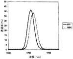
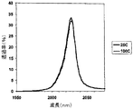
こうして製造したオプティカルコート製品での室温から約100℃の温度範囲での熱シフトは1nm程度であった。対照的に、ガラス基板上にコーティング層を堆積した対照製品の熱シフトは約7nmであった。これは図6及び図7の透過スペクトルで示される。図6は、25℃から100℃に加熱するとガラス基板上の多層体が7nmシフトすることを示し、図7はポリカーボネート基板上の多層体の性能を示すもので、デバイスを25℃から100℃に加熱しても実質的に移動しないことを示している。
【0033】
以上、例示のため典型的な実施形態について開示してきたが、以上の説明及び実施例は本発明の範囲を限定するものではない。本発明の技術的思想及び技術的範囲から逸脱せずに、様々な変更、適応、置換は当業者には自明であろう。
【図面の簡単な説明】
【0034】
【図1】従来技術のSiO2/a−Si:H多層コーティング系とSiO2/Ta2O5多層コーティング系の光学レスポンスの対比図である。
【図2】図1の従来技術のSiO2/Si多層コーティング系の屈折率プロファイルを厚さの関数として示すグラフである。
【図3】従来技術のSiO2/Ta2O5多層コーティング系の屈折率プロファイルを厚さの関数として示すグラフである。
【図4】本発明の1/4波長光学厚さ積層体の概略図である。
【図5】ポリカーボネート上に堆積した本発明の24層設計積層体の屈折率プロファイルを光学厚さの関数として示すグラフである。
【図6】ガラス上に堆積した本発明の24層積層体について測定した透過率を波長の関数として示すグラフである。
【図7】ポリカーボネート基板上に堆積した図4に示す24層積層体について測定した透過率を波長の関数として示すグラフである。
【符号の説明】
【0035】
400 オプティカルコート製品
420 ポリマー基板
440 非晶質水素化ケイ素層
460 二酸化ケイ素層【Technical field】
[0001]
The present invention relates to a product having an optical coating and a method for manufacturing the same. More specifically, the present invention relates to an optical coat product that exhibits a stable optical response to heat.
[Background]
[0002]
Optical coat products are useful as interference filters in applications such as thermo-optic switches. An optical coating product generally consists of a substrate having a number of coating layers, the substrate and the coating layer being transparent to light in various spectral ranges (typically visible and / or short wavelength infrared), and the coating layer having a high refractive index. Alternately with a low refractive index. The term “short wavelength infrared” refers to a region of about 700-2500 nm. The basic feature of a coating system is that there is a considerable difference in the refractive index of adjacent coating layers, typically with a refractive index ratio (hereinafter abbreviated as “R”) of about 1.5 or higher. expressed. A high ratio is often desirable.
[0003]
A typical optical coat product known in the art has alternating silicon oxide (SiO 2 ) and tantalum oxide (Ta 2 O 5 ) or titanium dioxide (TiO 2 ) coatings on a glass substrate. . Such product coating systems have R values of 1.5 or 1.6, respectively.
[0004]
It would be desirable to be able to produce optical products with high R values for coating systems (eg, greater than 2.0). Such a value can be obtained by using an alternating coating of silicon dioxide and amorphous silicon hydride (hereinafter referred to as “a-Si: H”) on a fused silica (ie, glass) substrate. The coating can be suitably deposited by plasma enhanced chemical vapor deposition (hereinafter referred to as “PECVD”). A total thickness of about 7.5 μm SiO 2 / a-SiH coating system consisting of 46 coating layers shows the same optical behavior as a 13 μm thick SiO 2 -Ta 2 O 5 coating system consisting of 64 layers There was found.
[0005]
The optical response of an optical product depends on the refractive index and thickness of the coating. Both of these characteristics are a function of temperature. The thermo-optic coefficient represents the change in the refractive index of the material as a function of temperature, and the thermomechanical coefficient, also known as the thermal expansion coefficient (hereinafter “CTE”), represents the change in physical dimensions with temperature.
[0006]
When glass is alternately coated with SiO 2 and a-SiH layers, the substrate CTE and the CTE of the coating and the thermo-optic coefficient cause significant changes in optical behavior with temperature. The main factor of this change is the relatively high thermo-optic coefficient of the a-SiH layer. Therefore, when heated, a shift of the interference structure (usually due to the center wavelength between the full width at half maximum (FWHM) of the reflected light) is observed. This shift is typically about 7 nm with a temperature change of 75 ° C. As mentioned above, the substrate CTE may be used to compensate for the optical shift of the coating.
[0007]
The CTE of the glass is about 7.8 ppm / ° C. Choosing the substrate so that the CTE of the substrate is as close as possible to 66 ppm / ° C minimizes the effect of temperature on the optical behavior (eg, the wavelength shift described above) because the CTE of the substrate substantially cancels the effect of the coating. To the limit. This is highly desirable.
DISCLOSURE OF THE INVENTION
[Problems to be solved by the invention]
[0008]
Therefore, it would be beneficial if an optical product with a reduced temperature change in optical performance could be developed.
[Means for Solving the Problems]
[0009]
The present invention provides an optical product in which the temperature change of the optical performance is almost negligible. A method of manufacturing such a product is also provided. The present invention is based on the discovery of an effect when a resin substrate having a CTE of about 70 ppm / ° C. is coated.
[0010]
In a first aspect, the present invention is an optical coat product comprising a polymer substrate and a plurality of coating layers, wherein the plurality of coating layers have alternating silicon dioxide layers and amorphous silicon hydride layers. And providing an optical coat product that is transparent in the short wavelength infrared spectral region.
[0011]
In a second aspect, the present invention is a method for producing an optically coated product comprising depositing a plurality of alternating coating layers of silicon dioxide and amorphous silicon hydride on a thermoplastic resin substrate, the method comprising: A method is provided for selecting a substrate such that the coated product is transparent in the short wavelength infrared spectral region.
BEST MODE FOR CARRYING OUT THE INVENTION
[0012]
In the following description, like reference numerals designate like or corresponding parts throughout the drawings of the accompanying drawings. Also, terms such as “upper”, “lower”, “outer”, “inner” are for convenience and should not be interpreted in a limiting sense.
[0013]
Referring generally to the accompanying drawings, and more particularly to FIG. 1, the illustration is intended to illustrate a preferred embodiment of the invention and is not intended to limit the invention.
[0014]
SiO 2 / a-Si of the prior art: H coating system having a layered structure shown below.
0.5H LHLHLHLHLHLHLHLHLHLHLHLHLHLHLHLHLHLHLHLHLHL 0.5H | Substrate Prior art SiO 2 / a-Si: H laminated structure is 46 layers of a-SiH (represented by “H”) and SiO 2 (represented by “L”). It consists of alternating layers and has a total thickness of about 7.5 μm. Each layer unit thickness corresponds to a quarter wavelength optical thickness.
[0015]
SiO 2 -Ta 2 O 5 coating systems of the prior art having a laminated structure shown below.
Air | 0.5H LHLHLHLHLHLHLHLHLHLHLHLHLHLHLHLHLHLHLHLHLHLHLHLHLHLHLHLHLHLHLHL 0.5H | Substrate Prior art SiO 2 / Ta 2 O 5 laminate structure is alternating between 64 layers of SiO 2 (represented by “L”) and Ta 2 O 5 (represented by “H”). It consists of layers and has a total thickness of about 13 μm. Each layer unit thickness corresponds to a quarter wavelength optical thickness.
[0016]
The SiO 2 / a-Si: H laminated structure and the SiO 2 / Ta 2 O 5 laminated structure show almost the same optical performance with respect to the reflectance as shown in FIG. The refractive index profiles for the SiO 2 / a-Si: H and SiO 2 / Ta 2 O 5 designs are shown in FIGS. 2 and 3, respectively.
[0017]
In the present invention, any thermoplastic resin substrate may be used as long as a product transparent to light in the short wavelength infrared spectrum region can be produced using the substrate.
[0018]
Particularly useful resins of this type include polymethyl methacrylate and aromatic polycarbonates, especially bisphenol A polycarbonates, ie polycarbonates derived from 2,2-bis (4-hydroxyphenyl) propane. Bisphenol A homopolycarbonate is particularly preferred.
[0019]
The thickness of the substrate is not critical for the purposes of the present invention. An exemplary thickness is about 1-50 mm. However, if the thickness of the substrate is too thick, there is a possibility that the absorption in a region having a near infrared region becomes high. Such absorption may or may not be a problem depending on the application.
[0020]
A plurality of coating layers composed of alternating layers of SiO 2 and a-Si: H are deposited on the substrate. Types of layers actually in contact with the substrate is not critical, SiO 2 and a-Si: none of the H are suitable. However, it is often convenient for the first layer to be a-Si: H. The coating configuration of the present invention can include up to about 500 layers. In one embodiment, about 10-100 layers can be deposited. In another embodiment, the plurality of coating layers consists of 1 to about 10 layers.
[0021]
Although the layer thickness is not so important, it is often advantageous that the thickness of a single layer corresponds to a quarter wavelength of light of a single wavelength probe value within the range of light to be transmitted. The thickness of each layer is related to other parameters as follows.
[0022]
L = mλ / 4n
Where L is the layer thickness, m is a multiple of the fundamental quarter wavelength optical unit (m = 1), λ is the wavelength of the probe, and n is the refractive index of the layer. Typically, a layer thickness of about 100-300 nm is used, but this value depends to some extent on the range of other relevant parameters. FIG. 4 shows a schematic of a
[0023]
The arrangement of the deposited layers may be periodic or aperiodic. Aperiodic layers are useful, for example, in computer-optimized designs or as additional layers to basic designs introduced for antireflection. Alternatively, the optical coating may have a symmetrical profile or various variations thereof. Such coatings are useful, for example, for bandpass filters, narrowband filters, long pass filters, or short pass filters.
[0024]
It is also within the technical scope of the present invention that the optical coating has a non-uniform laminated structure. One such non-uniform design is a sinusoidal periodic refractive index profile, commonly referred to as a “rugate” design.
[0025]
In another embodiment of the invention, the a-Si: H coating is doped with various elements known in the art, such as nitrogen, germanium, phosphorus, boron, carbon, and the like.
[0026]
The products of the present invention are typically manufactured by depositing the desired coating on a substrate. Any suitable deposition method can be used, but PECVD is preferred because PECVD is particularly suitable for such purposes. PECVD processes and equipment for their implementation are well known in the art. Each of the SiO 2 layer and the a-Si: H layer can be produced by plasma dissociation of an appropriate precursor. Typically, the precursor for a-Si: H is silane (SiH 4 ), and the precursor for SiO 2 is silane. Although it is a mixture of nitrous oxide (N 2 O), the molar ratio of nitrous oxide and silane in the latter mixture is typically about 20-100: 1. Suitable plasmas include noble gases, nitrogen, ammonia and hydrogen, and combinations thereof, although argon is often preferred. The deposition time for the desired thickness of the layer can be determined by simple contrast experiments under standard conditions with varying times.
【Example】
[0027]
The present invention is illustrated by way of example. In this example, a transparent bisphenol A homopolycarbonate substrate was coated with a silicon layer and then coated with alternating layers of SiO 2 and silicon for a total of 24 layers. 133nm, SiO 2 layer was 263nm. This design is called a narrowband path design. Such design requirements include high transmittance at a given wavelength and reflection of both the high and low wavelength sides in the vicinity thereof. A
[0028]
Air | LHLHLHLLHLHLHLHLHLHLLLHLHLH | Polycarbonate Here, H (represented by
[0029]
Each unit thick layer has a quarter wavelength optical thickness as described above. The refractive index profile for this design is shown in FIG. The scale is a unit of optical thickness, so the thickness of each unit layer is expressed in ¼ wavelength (0.25λ) increments. The 2 unit SiO 2 thickness (denoted “LL”) allows transmission at a predetermined wavelength and allows high reflection at wavelengths outside the center wavelength of the band.
[0030]
The silicon layer was deposited by PECVD of silane (supplied at a flow rate of 200 SCCM) using 200 millitorr of argon as the plasma gas (supplied at a flow rate of 1000 SCCM) and 200 watts of RF power. The SiO 2 layer was deposited by PECVD of silane (supplied at a flow rate of 200 SCCM). Silane was diluted to 2 mol% with argon. Dinitrogen oxide supplied at a flow rate of 200 SCCM was used as the plasma gas. The SiO 2 layer was deposited using the same pressure and power level. Silicon deposits in the following reaction,
SiH 4 (gas) → Si (solid film) + 2H 2 (gas)
Silicon oxide is deposited by the following reaction.
SiH 4 (gas) + 2N 2 O (gas) → SiO 2 (solid thin film) + N 2 , H 2 , NH 3 (gas)
[0031]
Due to incomplete dissociation of the precursor and low substrate temperature, the final composition is not in the exact stoichiometric ratio and contains significant impurities, especially hydrogen. This affects the optical properties to varying degrees.
[0032]
The thermal shift in the temperature range from room temperature to about 100 ° C. in the optical coat product thus manufactured was about 1 nm. In contrast, the thermal shift of the control product with the coating layer deposited on the glass substrate was about 7 nm. This is shown by the transmission spectra in FIGS. FIG. 6 shows that the multilayer on the glass substrate shifts by 7 nm when heated from 25 ° C. to 100 ° C., and FIG. 7 shows the performance of the multilayer on the polycarbonate substrate, from 25 ° C. to 100 ° C. It shows that even when heated, it does not move substantially.
[0033]
Although exemplary embodiments have been disclosed for illustrative purposes, the above description and examples are not intended to limit the scope of the invention. Various modifications, adaptations, and substitutions will be apparent to those skilled in the art without departing from the spirit and scope of the present invention.
[Brief description of the drawings]
[0034]
FIG. 1 is a comparison of the optical response of a prior art SiO 2 / a-Si: H multilayer coating system and a SiO 2 / Ta 2 O 5 multilayer coating system.
FIG. 2 is a graph showing the refractive index profile of the prior art SiO 2 / Si multilayer coating system of FIG. 1 as a function of thickness.
FIG. 3 is a graph showing the refractive index profile of a prior art SiO 2 / Ta 2 O 5 multilayer coating system as a function of thickness.
FIG. 4 is a schematic view of a quarter wavelength optical thickness laminate of the present invention.
FIG. 5 is a graph showing the refractive index profile of a 24-layer design laminate of the present invention deposited on polycarbonate as a function of optical thickness.
FIG. 6 is a graph showing the transmittance as a function of wavelength measured for a 24-layer laminate of the present invention deposited on glass.
7 is a graph showing the transmittance as a function of wavelength measured for the 24-layer stack shown in FIG. 4 deposited on a polycarbonate substrate.
[Explanation of symbols]
[0035]
400
Claims (27)
Applications Claiming Priority (2)
| Application Number | Priority Date | Filing Date | Title |
|---|---|---|---|
| US09/939,274 US6572975B2 (en) | 2001-08-24 | 2001-08-24 | Optically coated article and method for its preparation |
| PCT/US2002/025378 WO2003019244A1 (en) | 2001-08-24 | 2002-08-07 | Optically coated article and method for its preparation |
Publications (2)
| Publication Number | Publication Date |
|---|---|
| JP2005501286A true JP2005501286A (en) | 2005-01-13 |
| JP2005501286A5 JP2005501286A5 (en) | 2006-01-05 |
Family
ID=25472867
Family Applications (1)
| Application Number | Title | Priority Date | Filing Date |
|---|---|---|---|
| JP2003524053A Pending JP2005501286A (en) | 2001-08-24 | 2002-08-07 | Optical coat product and manufacturing method thereof |
Country Status (4)
| Country | Link |
|---|---|
| US (1) | US6572975B2 (en) |
| EP (1) | EP1421414A1 (en) |
| JP (1) | JP2005501286A (en) |
| WO (1) | WO2003019244A1 (en) |
Cited By (7)
| Publication number | Priority date | Publication date | Assignee | Title |
|---|---|---|---|---|
| JP2007079349A (en) * | 2005-09-16 | 2007-03-29 | Toray Ind Inc | Optical filter |
| KR101587643B1 (en) * | 2014-10-14 | 2016-01-25 | 광운대학교 산학협력단 | Non-iridescent Transmissive Structural Color Filter and manufacturing method thereof |
| KR20170117533A (en) * | 2015-02-18 | 2017-10-23 | 마테리온 코포레이션 | Near-infrared optical interference filter with improved transmission |
| JP2018504635A (en) * | 2015-01-23 | 2018-02-15 | マテリオン コーポレイション | Near-infrared optical interference filter with improved transmission |
| JP2020071375A (en) * | 2018-10-31 | 2020-05-07 | 日本電気硝子株式会社 | Band-pass filter and manufacturing method of the same |
| KR20200096892A (en) * | 2016-11-30 | 2020-08-14 | 비아비 솔루션즈 아이엔씨. | Silicon-germanium based optical filter |
| JP2022500706A (en) * | 2018-07-18 | 2022-01-04 | 福州高意光学有限公司Fuzhou Photop Optics Co., Ltd | Wide-angle application high-reflection mirror |
Families Citing this family (16)
| Publication number | Priority date | Publication date | Assignee | Title |
|---|---|---|---|---|
| US7045558B2 (en) * | 2003-08-29 | 2006-05-16 | General Electric Company | Method of making a high refractive index optical management coating and the coating |
| JP2008016799A (en) * | 2006-06-06 | 2008-01-24 | Mitsubishi Electric Corp | Semiconductor laser device |
| DE102009004251B3 (en) * | 2009-01-07 | 2010-07-01 | Ovd Kinegram Ag | Security element and method for producing a security element |
| KR101569406B1 (en) * | 2009-08-19 | 2015-11-17 | 주성엔지니어링(주) | Organic light emitting deivce and method for manufacturing the same |
| KR20110061422A (en) * | 2009-12-01 | 2011-06-09 | 엘지이노텍 주식회사 | Capacitance touch panel |
| TW202300961A (en) | 2012-07-16 | 2023-01-01 | 美商唯亞威方案公司 | Optical filter and sensor system |
| US9835952B2 (en) | 2013-03-14 | 2017-12-05 | Taiwan Semiconductor Manufacturing Company, Ltd. | Systems and methods for a narrow band high transmittance interference filter |
| DE102016002597A1 (en) * | 2016-03-04 | 2017-09-07 | Optics Balzers Ag | Broadband anti-reflection for the NIR range |
| US10644048B2 (en) * | 2017-02-01 | 2020-05-05 | Omnivision Technologies, Inc. | Anti-reflective coating with high refractive index material at air interface |
| CN108333661B (en) * | 2018-03-13 | 2024-01-02 | 湖北五方光电股份有限公司 | Low-angle offset optical filter based on boron doped silicon hydride and preparation method thereof |
| CN110824599B (en) | 2018-08-14 | 2021-09-03 | 白金科技股份有限公司 | Infrared band-pass filter |
| US11650361B2 (en) * | 2018-12-27 | 2023-05-16 | Viavi Solutions Inc. | Optical filter |
| EP3924723A1 (en) * | 2019-03-05 | 2021-12-22 | Quantum-Si Incorporated | Optical absorption filter for an integrated device |
| CN110109208A (en) * | 2019-06-05 | 2019-08-09 | 信阳舜宇光学有限公司 | Near-infrared bandpass filter and optical sensor system |
| CN112114394B (en) * | 2019-06-21 | 2023-03-31 | 福州高意光学有限公司 | Optical filter and sensor system with temperature compensation effect |
| CN112114402A (en) * | 2020-10-12 | 2020-12-22 | 东莞市微科光电科技有限公司 | CWDM optical filter |
Family Cites Families (12)
| Publication number | Priority date | Publication date | Assignee | Title |
|---|---|---|---|---|
| US4166919A (en) * | 1978-09-25 | 1979-09-04 | Rca Corporation | Amorphous silicon solar cell allowing infrared transmission |
| JPS59145588A (en) * | 1983-02-09 | 1984-08-21 | Hitachi Ltd | Semiconductor laser device |
| EP0173566A3 (en) * | 1984-08-29 | 1987-10-21 | Exxon Research And Engineering Company | Multi-layered material having graded properties |
| US4859553A (en) * | 1987-05-04 | 1989-08-22 | Xerox Corporation | Imaging members with plasma deposited silicon oxides |
| US4827870A (en) | 1987-10-05 | 1989-05-09 | Honeywell Inc. | Apparatus for applying multilayer optical interference coating on complex curved substrates |
| US5009920A (en) | 1990-03-30 | 1991-04-23 | Honeywell Inc. | Method for applying optical interference coating |
| US5245468A (en) * | 1990-12-14 | 1993-09-14 | Ford Motor Company | Anti-reflective transparent coating |
| FR2673633B1 (en) * | 1991-03-06 | 1993-06-11 | Air Liquide | MULTILAYER COATING FOR POLYCARBONATE SUBSTRATE. |
| US5694240A (en) * | 1994-06-24 | 1997-12-02 | Bausch & Lomb Incorporated | Multilayer anti-reflective and ultraviolet blocking coating for sunglasses |
| US6157503A (en) * | 1998-11-10 | 2000-12-05 | Thermo Vision Corporation | High performance optical filters suitable for intense ultraviolet irradiance applications |
| US6164777A (en) * | 1998-12-16 | 2000-12-26 | Bausch & Lomb Incorporated | Color-imparting contact lenses with interference coating and method for making the same |
| US6215802B1 (en) * | 1999-05-27 | 2001-04-10 | Blue Sky Research | Thermally stable air-gap etalon for dense wavelength-division multiplexing applications |
-
2001
- 2001-08-24 US US09/939,274 patent/US6572975B2/en not_active Expired - Fee Related
-
2002
- 2002-08-07 EP EP20020768483 patent/EP1421414A1/en not_active Withdrawn
- 2002-08-07 JP JP2003524053A patent/JP2005501286A/en active Pending
- 2002-08-07 WO PCT/US2002/025378 patent/WO2003019244A1/en active Application Filing
Cited By (16)
| Publication number | Priority date | Publication date | Assignee | Title |
|---|---|---|---|---|
| JP2007079349A (en) * | 2005-09-16 | 2007-03-29 | Toray Ind Inc | Optical filter |
| KR101587643B1 (en) * | 2014-10-14 | 2016-01-25 | 광운대학교 산학협력단 | Non-iridescent Transmissive Structural Color Filter and manufacturing method thereof |
| JP7075444B2 (en) | 2015-01-23 | 2022-05-25 | マテリオン コーポレイション | Near-infrared optical interferometer with improved transmittance |
| JP2018504635A (en) * | 2015-01-23 | 2018-02-15 | マテリオン コーポレイション | Near-infrared optical interference filter with improved transmission |
| JP2020149071A (en) * | 2015-01-23 | 2020-09-17 | マテリオン コーポレイション | Near-infrared optical interference filter with improved transmittance |
| JP2018506076A (en) * | 2015-02-18 | 2018-03-01 | マテリオン コーポレイション | Near-infrared optical interference filter with improved transmission |
| KR102583883B1 (en) * | 2015-02-18 | 2023-09-27 | 마테리온 코포레이션 | Near-infrared optical interference filter with improved transmission |
| US11372144B2 (en) | 2015-02-18 | 2022-06-28 | Materion Corporation | Near infrared optical interference filters with improved transmission |
| KR20170117533A (en) * | 2015-02-18 | 2017-10-23 | 마테리온 코포레이션 | Near-infrared optical interference filter with improved transmission |
| US11041982B2 (en) | 2016-11-30 | 2021-06-22 | Viavi Solutions Inc. | Silicon-germanium based optical filter |
| KR102392653B1 (en) * | 2016-11-30 | 2022-04-29 | 비아비 솔루션즈 아이엔씨. | Silicon-germanium based optical filter |
| KR20200096892A (en) * | 2016-11-30 | 2020-08-14 | 비아비 솔루션즈 아이엔씨. | Silicon-germanium based optical filter |
| JP2022500706A (en) * | 2018-07-18 | 2022-01-04 | 福州高意光学有限公司Fuzhou Photop Optics Co., Ltd | Wide-angle application high-reflection mirror |
| WO2020090615A1 (en) * | 2018-10-31 | 2020-05-07 | 日本電気硝子株式会社 | Band-pass filter and manufacturing method therefor |
| JP7251099B2 (en) | 2018-10-31 | 2023-04-04 | 日本電気硝子株式会社 | Bandpass filter and manufacturing method thereof |
| JP2020071375A (en) * | 2018-10-31 | 2020-05-07 | 日本電気硝子株式会社 | Band-pass filter and manufacturing method of the same |
Also Published As
| Publication number | Publication date |
|---|---|
| EP1421414A1 (en) | 2004-05-26 |
| US6572975B2 (en) | 2003-06-03 |
| WO2003019244A1 (en) | 2003-03-06 |
| US20030039847A1 (en) | 2003-02-27 |
Similar Documents
| Publication | Publication Date | Title |
|---|---|---|
| JP2005501286A (en) | Optical coat product and manufacturing method thereof | |
| US11022733B2 (en) | ASi-H bandpass filter comprising a second material with high refractive index and a second bandpass filter as a blocker | |
| Jin et al. | Design, formation and characterization of a novel multifunctional window with VO 2 and TiO 2 coatings | |
| Lee et al. | Omnidirectional Flexible Transmissive Structural Colors with High‐Color‐Purity and High‐Efficiency Exploiting Multicavity Resonances | |
| US20170357033A1 (en) | Protected item including a protective coating | |
| US11402559B2 (en) | Optical filter with layers having refractive index greater than 3 | |
| JP2007534007A (en) | Films for optical applications and methods for making such films | |
| US6793981B2 (en) | Process for producing laminated film, and reflection reducing film | |
| JPH01500041A (en) | Method of forming environmentally stable optical coatings | |
| WO1985001115A1 (en) | Process for forming a graded index optical material and structures formed thereby | |
| US20090311521A1 (en) | Thin film and optical interference filter incorporating high-index titanium dioxide and method for making them | |
| Qiu et al. | Resonant transmission and frequency trifurcation of light waves in Thue-Morse dielectric multilayers | |
| US20110102926A1 (en) | Mirror and process for obtaining a mirror | |
| JP2023178283A (en) | Ultra-thin thin-film optical interference filter | |
| WO2021220089A1 (en) | Reflective optical metasurface films | |
| CA3087719A1 (en) | Multispectral interference coating with diamond-like carbon (dlc) film | |
| KR20180048981A (en) | Flexible Bragg reflector | |
| JP5132902B2 (en) | Antireflection film for passband of photonic band gap crystal | |
| US20120120514A1 (en) | Structure comprising at least one reflecting thin-film on a surface of a macroscopic object, method for fabricating a structure, and uses for the same | |
| Desu | Metallorganic chemical vapor deposition: a new era in optical coating technology | |
| KR100762204B1 (en) | Method for fabricating optical multi-layer thin film | |
| Amri et al. | Optical modeling and investigation of thin films based on plasma-polymerized HMDSO under oxygen flow deposited by PECVD | |
| JP2006220899A (en) | Manufacturing method of phase level difference element | |
| CN117631101A (en) | Low reflection film system structure and method for manufacturing same | |
| Poitras et al. | Asymmetrical dual-cavity filters: theory and application |
Legal Events
| Date | Code | Title | Description |
|---|---|---|---|
| A521 | Request for written amendment filed |
Free format text: JAPANESE INTERMEDIATE CODE: A523 Effective date: 20050803 |
|
| A621 | Written request for application examination |
Free format text: JAPANESE INTERMEDIATE CODE: A621 Effective date: 20050803 |
|
| RD13 | Notification of appointment of power of sub attorney |
Free format text: JAPANESE INTERMEDIATE CODE: A7433 Effective date: 20070903 |
|
| A131 | Notification of reasons for refusal |
Free format text: JAPANESE INTERMEDIATE CODE: A131 Effective date: 20080812 |
|
| A02 | Decision of refusal |
Free format text: JAPANESE INTERMEDIATE CODE: A02 Effective date: 20090310 |