JP2005301222A - Display device - Google Patents

Display device Download PDF

Info

Publication number
JP2005301222A
JP2005301222A JP2004372739A JP2004372739A JP2005301222A JP 2005301222 A JP2005301222 A JP 2005301222A JP 2004372739 A JP2004372739 A JP 2004372739A JP 2004372739 A JP2004372739 A JP 2004372739A JP 2005301222 A JP2005301222 A JP 2005301222A
Authority
JP
Japan
Prior art keywords
light
optical waveguide
waveguide plate
display device
layer
Prior art date
Legal status (The legal status is an assumption and is not a legal conclusion. Google has not performed a legal analysis and makes no representation as to the accuracy of the status listed.)
Pending
Application number
JP2004372739A
Other languages
Japanese (ja)
Other versions
JP2005301222A5 (en
Inventor
Kenichi Iwauchi
謙一 岩内
Kei Tokui
圭 徳井
Yukihisa Takeuchi
幸久 武内
Tsutomu Nanataki
七瀧  努
Natsuki Shimokawa
夏己 下河
Isao Yomo
功 四方
Current Assignee (The listed assignees may be inaccurate. Google has not performed a legal analysis and makes no representation or warranty as to the accuracy of the list.)
NGK Insulators Ltd
Sharp Corp
Original Assignee
NGK Insulators Ltd
Sharp Corp
Priority date (The priority date is an assumption and is not a legal conclusion. Google has not performed a legal analysis and makes no representation as to the accuracy of the date listed.)
Filing date
Publication date
Application filed by NGK Insulators Ltd, Sharp Corp filed Critical NGK Insulators Ltd
Priority to JP2004372739A priority Critical patent/JP2005301222A/en
Priority to US11/083,358 priority patent/US7444052B2/en
Publication of JP2005301222A publication Critical patent/JP2005301222A/en
Publication of JP2005301222A5 publication Critical patent/JP2005301222A5/ja
Pending legal-status Critical Current

Links

Images

Classifications

    • GPHYSICS
    • G02OPTICS
    • G02BOPTICAL ELEMENTS, SYSTEMS OR APPARATUS
    • G02B6/00Light guides; Structural details of arrangements comprising light guides and other optical elements, e.g. couplings
    • G02B6/0001Light guides; Structural details of arrangements comprising light guides and other optical elements, e.g. couplings specially adapted for lighting devices or systems
    • G02B6/0011Light guides; Structural details of arrangements comprising light guides and other optical elements, e.g. couplings specially adapted for lighting devices or systems the light guides being planar or of plate-like form
    • G02B6/0033Means for improving the coupling-out of light from the light guide

Abstract

<P>PROBLEM TO BE SOLVED: To improve the utility efficiency of light in a composition in which some regions of a liquid crystal panel is selectively irradiated with light or a region irradiated with light is moved stepwise according to the period of the vertical scanning signal of the liquid crystal. <P>SOLUTION: A display device includes a lighting system 10A which has: an optical waveguide plate 38 for introducing light thereinto; a drive part 36 having a planar array of actuators 34 disposed in facing relation to the optical waveguide plate 38; a displacement transmission part 39 disposed between the optical waveguide plate 38 and the drive part 36; and a light scattering layer 80 disposed on the displacement transmission part 39, and which controls light that leaks from the optical waveguide plate 38 as emitted light, by selective contact/separation of the light scattering layer 80 with/from the optical waveguide plate 38 caused by the drive part 36. The display device also includes a liquid crystal panel 12 for modulating the emitted light from the lighting system 10A to display an image. The lighting system 10A has a light reflecting layer 300 disposed on at least a portion of the displacement transmission part 39 that confronts the optical waveguide plate 38. <P>COPYRIGHT: (C)2006,JPO&NCIPI

Description

本発明は、光導波板からの出射光を変調して画像を表示する表示装置に関する。   The present invention relates to a display device that displays an image by modulating light emitted from an optical waveguide plate.

パーソナルコンピュータやテレビジョン受像機の表示装置として、ブラウン管(CRT:Cathod Ray Tube、以下「CRT」と称する。)が広く用いられているが、CRTは装置全体のサイズが大きいことや、消費電力が大きいこと等から、液晶ディスプレイ(LCD:Liquid Crystal Display、以下「LCD」と称する。)が急速に普及しつつある。   As a display device for a personal computer or a television receiver, a cathode ray tube (CRT: Cathode Ray Tube; hereinafter referred to as “CRT”) is widely used. Due to its large size and the like, a liquid crystal display (LCD: Liquid Crystal Display, hereinafter referred to as “LCD”) is rapidly spreading.

しかしながら、LCDは、動画像を表示させた場合に、いわゆる尾引きと呼ばれる残像現象が生じてしまう。これは、ホールド型表示と呼ばれる表示原理によるものであり、ホールド型表示とは、画像を表示する1フレームの期間中ほぼ一定の表示を行う表示をいう。ホールド型表示の場合、あるフレーム期間と次のフレーム期間で画像が変化する場合(すなわち動画像)、そのフレーム間の瞬間において同時に異なる位置で表示されたかのように見えるため、残像感を生じてしまう。これに対し、CRTは、非ホールド型(インパルス型)表示と呼ばれ、1フレーム中にある瞬間だけ発光するもので、その瞬間ごとの目で追いかけることにより残像感を生じない。   However, when a moving image is displayed on the LCD, an afterimage phenomenon called so-called tailing occurs. This is based on a display principle called hold-type display. The hold-type display refers to a display that performs a substantially constant display during one frame period for displaying an image. In the case of hold-type display, when an image changes between a certain frame period and the next frame period (that is, a moving image), it appears as if it was displayed at different positions at the same time between the frames, resulting in an afterimage feeling. . On the other hand, the CRT is called a non-hold type (impulse type) display and emits light only at a certain moment in one frame, and an afterimage is not caused by chasing with the eyes at each moment.

このホールド型表示による残像現象を改善する方法として、例えば図25に示すように、表示素子(液晶)1000の前面(観測者1002側)あるいは後面(光源ランプ1004側)にシャッタ1006を配置する方法がある(第1の方法)。表示素子1000は、駆動回路1008からの駆動信号に基づいて光源ランプ1004からの光を変調することにより画像を表示する。シャッタ1006は、パルス発生回路1010からのシャッタ制御パルスに基づいて表示素子1000からの表示光の透過を制御する(例えば特許文献1参照)。   As a method of improving the afterimage phenomenon due to the hold-type display, for example, as shown in FIG. 25, a shutter 1006 is arranged on the front surface (observer 1002 side) or rear surface (light source lamp 1004 side) of the display element (liquid crystal) 1000. (First method). The display element 1000 displays an image by modulating light from the light source lamp 1004 based on a drive signal from the drive circuit 1008. The shutter 1006 controls transmission of display light from the display element 1000 based on a shutter control pulse from the pulse generation circuit 1010 (see, for example, Patent Document 1).

つまり、シャッタ1006によって光源ランプ1004からの光をオン/オフ制御することにより、毎フレームのある期間だけ表示素子1000からの表示画像を観測者1002に向けて表示させることで、擬似的にインパルス型表示を実現することができる。   That is, by controlling on / off of the light from the light source lamp 1004 by the shutter 1006, the display image from the display element 1000 is displayed toward the observer 1002 only for a certain period of each frame, so that the pseudo impulse type Display can be realized.

また、図26に示すように、シャッタ1006を配置する代わりに、パルス発生回路1010から制御パルスを光源の電源に供給する方法がある(第2の方法)。すなわち、電源1012から光源ランプ1004への電力供給を前記制御パルスに基づいてオン/オフ制御し、光源ランプ1004を点灯/消灯させることで、毎フレームのある期間だけ表示素子100からの表示画像を観測者1002に向けて表示させるというものである。この場合も、擬似的にインパルス型表示を実現することができる(同じく特許文献1参照)。なお、レンズ1014は、表示素子1000からの画像表示光をスクリーン1016に結像させる。   As shown in FIG. 26, there is a method of supplying a control pulse from the pulse generation circuit 1010 to the power source of the light source instead of arranging the shutter 1006 (second method). That is, the power supply from the power source 1012 to the light source lamp 1004 is turned on / off based on the control pulse, and the light source lamp 1004 is turned on / off to display a display image from the display element 100 for a certain period of each frame. The display is made for the observer 1002. Also in this case, a pseudo impulse type display can be realized (see also Patent Document 1). The lens 1014 focuses the image display light from the display element 1000 on the screen 1016.

また、図27に示すように、液晶表示部1020の後面に照明装置1022を配置した液晶表示装置1024において、動画のぼけを防止するために照明装置1022を複数の領域(領域Za、領域Zb及び領域Zc)に分割し、各領域毎に液晶表示部1020を照射するように照明ドライバ1026によって照明装置1022を制御する方法がある(第3の方法)。   In addition, as shown in FIG. 27, in the liquid crystal display device 1024 in which the illumination device 1022 is arranged on the rear surface of the liquid crystal display unit 1020, the illumination device 1022 is divided into a plurality of regions (region Za, region Zb, and There is a method in which the illumination device 1022 is controlled by the illumination driver 1026 so as to divide the region Zc) and irradiate the liquid crystal display unit 1020 for each region (third method).

照明装置1022は、液晶表示部1020に接する上部に光拡散板1028が設置され、その下には複数のランプ1030が設置され、さらに、ランプ1030の下部に光反射板1032が設置されて構成されている。   The illuminating device 1022 includes a light diffusing plate 1028 installed at an upper part in contact with the liquid crystal display unit 1020, a plurality of lamps 1030 installed below the lighting device 1022, and a light reflecting plate 1032 installed at the lower part of the lamp 1030. ing.

そして、照明ドライバ1026は、液晶コントローラ1034からの垂直同期信号Sv及び水平同期信号Shに基づいて照明装置1022における領域Za、領域Zb及び領域Zcの3つの領域毎のランプ1030の点灯、消灯を制御する。例えば照明ドライバ1026によって、照明装置1022の各領域のランプ1030を、液晶表示部1020の透過率が飽和状態のなった後に点灯されるように制御する。これにより、静止画を視角速度10度/秒の速度で動かした動画を表示させても、特に画像のぼけはまったく感じられないものとすることができる(例えば特許文献2参照)。   The lighting driver 1026 controls lighting and extinguishing of the lamp 1030 for each of the three areas of the area Za, the area Zb, and the area Zc in the lighting device 1022 based on the vertical synchronization signal Sv and the horizontal synchronization signal Sh from the liquid crystal controller 1034. To do. For example, the lighting driver 1026 controls the lamps 1030 in each region of the lighting device 1022 so that the lamps 1030 are turned on after the transmittance of the liquid crystal display unit 1020 is saturated. As a result, even when a moving image in which a still image is moved at a viewing angle speed of 10 degrees / second is displayed, it is possible to prevent the image from being particularly blurred (see, for example, Patent Document 2).

また、ランプ1030を点灯/消灯させる代わりに、ランプ1030と液晶表示部1020間に液晶によるシャッタ(図示せず)を設け、該シャッタでのランプ1030からの光の吸収と透過を制御することで、前記第3の方法と同様に、液晶表示部1020に対して複数の領域毎にインパルス型表示を実現する方法もある(第4の方法:同じく特許文献2参照)。   Further, instead of turning on / off the lamp 1030, a shutter (not shown) made of liquid crystal is provided between the lamp 1030 and the liquid crystal display unit 1020, and absorption and transmission of light from the lamp 1030 by the shutter are controlled. Similarly to the third method, there is also a method for realizing an impulse-type display for each of a plurality of regions on the liquid crystal display unit 1020 (fourth method: see also Patent Document 2).

これら第3及び第4の方法においては、画面全体の一括によるインパルス型表示(第1及び第2の方法)と比較して、液晶表示部1020に対する走査に合わせて各領域の発光のタイミングをずらしていくことができることから、液晶の応答時間と発光時間の制約がより緩やかになり、点灯時間が長くなるため、発光強度を上げる必要がなくなる、という効果を奏する。   In these third and fourth methods, the timing of light emission in each region is shifted in accordance with the scanning with respect to the liquid crystal display unit 1020, as compared with the impulse-type display (first and second methods) in which the entire screen is batched. Therefore, the restrictions on the response time and the light emission time of the liquid crystal become more gradual, and the lighting time becomes longer, so that it is not necessary to increase the light emission intensity.

また、照明装置を使用した方法としては、その他、例えば特許文献3に記載された方法がある。図28に示すように、この照明装置1040は、アクリルである一対の導光体1042及び1044と、一方がストライプ状となるよう導光体1042及び1044上に形成された透明電極1046及び1048と、一対の導光体1042及び1044に挟持されるポリマー分散型液晶層1050と、導光体1044の下面に設けられた空気層1052と、空気層1052を介して導光体1044の下面に設けられた第1の反射板1054と、一対の導光体1042及び1044の側面に配置された光源1056と、光源1056を覆う光源カバー1058と、もう一方の側面に配置された第2の反射板1060とを有する。   Moreover, as a method using an illuminating device, there is a method described in Patent Document 3, for example. As shown in FIG. 28, this lighting device 1040 includes a pair of light guides 1042 and 1044 made of acrylic, and transparent electrodes 1046 and 1048 formed on the light guides 1042 and 1044 so that one of them is in a stripe shape. A polymer dispersed liquid crystal layer 1050 sandwiched between the pair of light guides 1042 and 1044, an air layer 1052 provided on the lower surface of the light guide 1044, and provided on the lower surface of the light guide 1044 via the air layer 1052. First reflecting plate 1054, a light source 1056 disposed on the side surfaces of the pair of light guides 1042 and 1044, a light source cover 1058 covering the light source 1056, and a second reflecting plate disposed on the other side surface 1060.

そして、一部のポリマー分散型液晶層1050に対して電場印加(例えば30Vを印加する。)することにより透過状態1062に、一部のポリマー分散型液晶層1050に対して電圧無印加(例えば0Vとする。)とすることにより散乱状態1064とする。入射光1066が透過状態1062に入射された場合、散乱されることなくそのまま導光体1042の内部を伝播し、導光体1042の界面で全反射し、反射光1068となる。よって反射光1068は同様に全反射を繰返しながら導光体中を伝播していくことになる。一方、散乱状態1064へ入射した場合は、光は散乱を受けて散乱光1070及び1072となる。そして、散乱光1070(上方を向いた散乱光)の導光体界面に対する入射角は全反射角より小さくなるので、導光体1042より出射されることとなる。一方、散乱光1072(下方を向いた散乱光)の導光体界面に対する入射角も同様に、全反射角より小さくなっているため、導光体下方向へ出射し、照明装置1040下部の第1の反射板1054で反射、再度の照明装置1040への入射等を経て、導光体1042上方に出射されることとなる。つまり、照明装置1040における散乱状態の部分から光が放出される。   Then, by applying an electric field (for example, applying 30 V) to a part of the polymer dispersed liquid crystal layer 1050, no voltage is applied to the part of the polymer dispersed liquid crystal layer 1050 (for example, 0 V). )) To obtain a scattering state 1064. When the incident light 1066 enters the transmission state 1062, it propagates as it is inside the light guide 1042 without being scattered, and is totally reflected at the interface of the light guide 1042 to become reflected light 1068. Therefore, the reflected light 1068 propagates through the light guide body while repeating total reflection in the same manner. On the other hand, when incident on the scattering state 1064, the light is scattered and becomes scattered light 1070 and 1072. The incident angle of the scattered light 1070 (scattered light facing upward) with respect to the light guide interface is smaller than the total reflection angle, and thus is emitted from the light guide 1042. On the other hand, since the incident angle of the scattered light 1072 (scattered light directed downward) with respect to the light guide interface is also smaller than the total reflection angle, the light is emitted downwardly, and the first light beam below the illumination device 1040 is emitted. The light is reflected by one reflector 1054, re-incident on the illumination device 1040, and the like, and is emitted above the light guide body 1042. That is, light is emitted from the scattered state portion of the lighting device 1040.

この照明装置1040を利用して、光源1056からの光の透過と散乱の状態を制御することで、画像の領域毎にインパルス型表示を実現することができる。これにより、光の吸収なしに領域毎の光の出射を制御できる。   By using the lighting device 1040 to control the state of transmission and scattering of light from the light source 1056, an impulse-type display can be realized for each region of the image. Thereby, the emission of light for each region can be controlled without light absorption.

また、光導波板とアクチュエータを用い、光導波板からの漏光を領域毎に制御した表示装置が開示されている(例えば特許文献4参照)。この表示装置1080は、図29に示すように、光導波板1082の端面に光源(図示せず)を配置し、アクチュエータ1084を光導波板1082の表示面と反対の面に配置し、アクチュエータ1084あるいはアクチュエータ1084に接続された変位伝達部1086を光導波板1082に接触させることで、光導波板1082内を伝搬する光1088を選択的に出射させる。アクチュエータ1084に接続された変位伝達部1086が光導波板1082に接触していない場合は、通常の光導波板1082と同様に全反射条件により光導波板1082内を光1088が伝搬するが、変位伝達部1086が光導波板1082に接触した場合、光導波板1082の全反射条件が成り立たなくなり、光導波板1082の表示面のうち、変位伝達部1086が接触した部位に対応する箇所から光(漏光)1090が出射する。これにより、任意の領域から光を出射することが可能となり、画像表示等を実現することができる。   Further, a display device is disclosed in which light leakage from the optical waveguide plate is controlled for each region using an optical waveguide plate and an actuator (see, for example, Patent Document 4). In this display device 1080, as shown in FIG. 29, a light source (not shown) is disposed on the end surface of the optical waveguide plate 1082, the actuator 1084 is disposed on the surface opposite to the display surface of the optical waveguide plate 1082, and the actuator 1084 is disposed. Alternatively, the displacement transmitting portion 1086 connected to the actuator 1084 is brought into contact with the optical waveguide plate 1082 to selectively emit the light 1088 propagating through the optical waveguide plate 1082. When the displacement transmitting portion 1086 connected to the actuator 1084 is not in contact with the optical waveguide plate 1082, the light 1088 propagates in the optical waveguide plate 1082 under the total reflection condition as in the case of the normal optical waveguide plate 1082, but the displacement When the transmission unit 1086 comes into contact with the optical waveguide plate 1082, the total reflection condition of the optical waveguide plate 1082 is not satisfied, and light (from the portion corresponding to the portion with which the displacement transmission unit 1086 is in contact on the display surface of the optical waveguide plate 1082). Leakage light) 1090 is emitted. As a result, light can be emitted from an arbitrary region, and image display or the like can be realized.

特開平9−325715号公報JP-A-9-325715 特開2000−275604号公報JP 2000-275604 A 特開2002−49037号公報JP 2002-49037 A 特開平7−287176号公報JP 7-287176 A

しかしながら、従来の上述した方法では、以下のような問題がある。特許文献1及び2記載の表示装置においては、シャッタを用いるか、あるいは光源を点灯させたり消灯させたりすることで、インパルス型表示を実現しているが、シャッタによる光のオン/オフ制御では、光を吸収させることでオフ状態を実現するため、光の利用効率が低下してしまう。つまり、輝度の低下、もしくは輝度を一定に保とうとすれば、消費電力の増加を引き起こす。また、光源を点灯させたり消灯させたりする制御では、光源として冷陰極線管を用いた表示装置の光源の寿命が短くなる上に、点灯(消灯)させたい領域毎に光源を配置しなくてはならず、コストの増加と表示装置の大型化が生じる。さらには、光のオフ状態を実現する領域では光源は使われないため、光源の利用効率が悪いといえる。   However, the conventional method described above has the following problems. In the display devices described in Patent Documents 1 and 2, impulse-type display is realized by using a shutter or by turning on and off a light source. However, in the light on / off control by the shutter, Since the off state is realized by absorbing light, the light use efficiency is lowered. That is, if the brightness is reduced or the brightness is kept constant, the power consumption is increased. In the control of turning on and off the light source, the life of the light source of the display device using the cold cathode ray tube as the light source is shortened, and a light source must be arranged for each area to be turned on (turned off). In other words, the cost increases and the size of the display device increases. Furthermore, since the light source is not used in the region where the light is turned off, it can be said that the use efficiency of the light source is poor.

特許文献3に記載の表示装置は、光を吸収させるシャッタを必要とせず、光源も常時発光でよく、領域毎に光のオン/オフが制御可能であるが、光の透過、散乱に液晶を用いており、光を透過させる状態、つまり、全反射を行って光導波板を導波する領域(すなわち光出射させない領域)においても液晶を透過するが、液晶は光の透過率が高くないため、光の損失が生じる。1回や2回の透過であれば、微々たる光損失であっても、光導波板では幾重にも繰り返し全反射が行われるため、何度も液晶層を通過し、その損失は通過する回数の累乗で効いてくるため、光の利用効率がよいとはいえない。   The display device described in Patent Document 3 does not require a shutter for absorbing light, and the light source may always emit light, and the on / off of light can be controlled for each region, but liquid crystal is used for transmission and scattering of light. The liquid crystal is transmitted even in a state where light is transmitted, that is, a region where total reflection is performed and the light is guided through the optical waveguide plate (that is, a region where light is not emitted), but the liquid crystal is not high in light transmittance. Loss of light occurs. If the light is transmitted once or twice, even if it is a slight light loss, the optical waveguide plate repeatedly and repeatedly performs total reflection, so it passes through the liquid crystal layer many times, and the loss is the number of times it passes. Because it works with the power of, it cannot be said that the light use efficiency is good.

特許文献4に記載の表示装置は、光を吸収させるシャッタを必要とせず、光源も常時発光でよく、領域毎に光のオン/オフを制御可能であるが、光導波板で全反射が成り立たなくなり、直接変位伝達部に照射される光の利用のみを考えており、その他の部位や変位伝達部への照射後の光の有効利用は考えられていなかった。特に、光導波板の表示面側に、さらに光学部材を付加する構成は想定されてなく、光学部品のメリットを活かせず、光の有効利用はされていない。   The display device described in Patent Document 4 does not require a shutter for absorbing light, and the light source may always emit light, and the on / off of light can be controlled for each region, but total reflection is realized by the optical waveguide plate. Only the use of light directly irradiating the displacement transmission unit is considered, and effective use of light after irradiation to other parts and the displacement transmission unit has not been considered. In particular, a configuration in which an optical member is further added to the display surface side of the optical waveguide plate is not assumed, the advantages of the optical component are not utilized, and light is not effectively used.

本発明はこのような課題を考慮してなされたものであり、ホールド型表示を擬似的にインパルス型表示することで、動画質の表示特性の改善を図ることができ、さらには、光の利用効率の向上を図ることができる表示装置を提供することを目的とする。   The present invention has been made in consideration of such problems, and it is possible to improve the display characteristics of moving image quality by pseudo-impulse-type display of hold-type display, and further, use of light It is an object to provide a display device capable of improving efficiency.

本発明に係る表示装置は、光が導入される光導波板と、前記光導波板に対向して複数のアクチュエータ部が平面的に配列された駆動部と、前記光導波板と前記駆動部との間に形成された変位伝達部と、前記変位伝達部上に形成された光散乱層とを有し、前記駆動部による選択的な前記光導波板への接触・離隔によって、前記光導波板からの漏光を出射光として制御する照明装置と、前記照明装置からの出射光を変調して画像を表示する光変調装置とを有する表示装置であって、前記光導波板と対向する前記駆動部の上部に光反射層が形成されていることを特徴とする。   The display device according to the present invention includes an optical waveguide plate into which light is introduced, a drive unit in which a plurality of actuator units are arranged in a plane facing the optical waveguide plate, the optical waveguide plate, and the drive unit. And a light scattering layer formed on the displacement transmission unit, and the optical waveguide plate is selectively contacted and separated from the optical waveguide plate by the driving unit. A display device comprising: an illuminating device that controls leakage light from the illuminating light as emitted light; and a light modulating device that modulates the emitted light from the illuminating device to display an image, wherein the driving unit faces the optical waveguide plate A light reflecting layer is formed on the top of the substrate.

ここで、「駆動部の上部」とは、前記変位伝達部の上部(上部の一部を含む)や、前記駆動部の上部(上部の一部を含む)を含む。   Here, the “upper part of the drive unit” includes the upper part (including a part of the upper part) of the displacement transmission part and the upper part (including a part of the upper part) of the drive part.

これにより、まず、駆動部によるアクチュエータ部に対する変位駆動によって、光散乱層を光導波板に接触させることで、光導波板の主面(光が出射する面)から光が出射されることになる。本発明では、前記光導波板と対向する前記駆動部の上部に光反射層を形成するようにしているため、光導波板の主面から効率よく光を出射させることができる。   Accordingly, first, light is emitted from the main surface (surface from which light is emitted) of the optical waveguide plate by bringing the light scattering layer into contact with the optical waveguide plate by displacement driving of the actuator unit with respect to the actuator unit. . In the present invention, since the light reflecting layer is formed on the drive unit facing the optical waveguide plate, light can be efficiently emitted from the main surface of the optical waveguide plate.

また、駆動部によるアクチュエータ部に対する選択的な変位駆動によって、一部の光散乱層を光導波板に接触させることで、光導波板の主面のうち、一部から光が出射されることになる。すなわち、光導波板の主面の一部から選択的に光を出射させることができる。しかも、駆動部によるアクチュエータ部に対する選択的な変位駆動をある周期に従って制御することで光の出射領域を段階的に移動させることができる。   In addition, light is emitted from a part of the main surface of the optical waveguide plate by bringing a part of the light scattering layer into contact with the optical waveguide plate by selectively driving the actuator with respect to the actuator unit. Become. That is, light can be selectively emitted from a part of the main surface of the optical waveguide plate. In addition, the light emission region can be moved stepwise by controlling the selective displacement driving of the actuator by the driving unit according to a certain period.

つまり、本発明に係る表示装置においては、光変調装置の表示原理がホールド型表示であった場合に、擬似的にインパルス型表示させることができ、動画質の表示特性の改善を図ることができ、しかも、光の利用効率の向上を図ることができる。   In other words, in the display device according to the present invention, when the display principle of the light modulation device is the hold type display, it is possible to make a pseudo impulse type display and to improve the display characteristics of the moving image quality. In addition, the light utilization efficiency can be improved.

また、本発明に係る表示装置は、光が導入される光導波板と、前記光導波板に対向して複数のアクチュエータ部が平面的に配列された駆動部と、前記光導波板と前記駆動部との間に形成された変位伝達部と、前記変位伝達部上に形成された光散乱層とを有し、前記駆動部による選択的な前記光導波板への接触・離隔によって、前記光導波板からの漏光を出射光として制御する照明装置と、前記照明装置からの出射光を変調して画像を表示する光変調装置とを有する表示装置であって、前記光導波板と対向する前記変位伝達部の少なくとも一部に光反射層が形成されていることを特徴とする。   Further, the display device according to the present invention includes an optical waveguide plate into which light is introduced, a drive unit in which a plurality of actuator units are arranged in a plane facing the optical waveguide plate, the optical waveguide plate, and the drive And a light scattering layer formed on the displacement transmission part, and the driving part selectively contacts and separates the optical waveguide plate from the optical waveguide. A display device comprising: an illuminating device that controls leakage light from a corrugated plate as emitted light; and a light modulation device that modulates emitted light from the illuminating device to display an image, wherein the display device faces the optical waveguide plate. A light reflecting layer is formed on at least a part of the displacement transmitting portion.

これにより、光導波板の主面から効率よく光を出射させることができる。従って、この発明においても、光変調装置の表示原理がホールド型表示であった場合に、擬似的にインパルス型表示させることができ、動画質の表示特性の改善を図ることができ、しかも、光の利用効率の向上を図ることができる。   Thereby, light can be efficiently emitted from the main surface of the optical waveguide plate. Therefore, also in the present invention, when the display principle of the light modulation device is the hold type display, it is possible to make a pseudo impulse type display, to improve the display characteristics of the moving image quality, The utilization efficiency can be improved.

そして、前記構成において、前記光導波板と対向する前記変位伝達部の少なくとも一部に形成された前記光反射層上に、前記変位伝達部上に形成された前記光散乱層を形成するようにしてもよい。この場合、光源の薄型化を図るために、光散乱層の厚みを薄くすることが考えられるが、該光散乱層を薄くすると、光散乱層に入射した光が該光散乱層を通過し、発光として寄与しなくなるおそれがある。しかし、光散乱層の下層に光反射層を形成することで、該光散乱層を通過した光を反射させることができ、光散乱層を薄くすることによる輝度低下を抑えることができる。   And in the said structure, the said light-scattering layer formed on the said displacement transmission part is formed on the said light reflection layer formed in at least one part of the said displacement transmission part facing the said optical waveguide plate. May be. In this case, it is conceivable to reduce the thickness of the light scattering layer in order to reduce the thickness of the light source. However, if the light scattering layer is thinned, the light incident on the light scattering layer passes through the light scattering layer, There is a possibility that it may not contribute as light emission. However, by forming a light reflecting layer below the light scattering layer, the light that has passed through the light scattering layer can be reflected, and a reduction in luminance due to the thin light scattering layer can be suppressed.

また、本発明に係る表示装置は、光が導入される光導波板と、前記光導波板に対向して複数のアクチュエータ部が平面的に配列された駆動部と、前記光導波板と前記駆動部との間に形成された変位伝達部と、前記変位伝達部上に形成された光散乱層とを有し、前記駆動部による選択的な前記光導波板への接触・離隔によって、前記光導波板からの漏光を出射光として制御する照明装置と、前記照明装置からの出射光を変調して画像を表示する光変調装置とを有する表示装置であって、前記光導波板と対向する前記駆動部の少なくとも一部に光反射層が形成されていることを特徴とする。これにより、駆動部まで進入した迷光を光導波板の前方に向けて反射させることができる。   Further, the display device according to the present invention includes an optical waveguide plate into which light is introduced, a drive unit in which a plurality of actuator units are arranged in a plane facing the optical waveguide plate, the optical waveguide plate, and the drive And a light scattering layer formed on the displacement transmission part, and the driving part selectively contacts and separates the optical waveguide plate from the optical waveguide. A display device comprising: an illuminating device that controls leakage light from a corrugated plate as emitted light; and a light modulation device that modulates emitted light from the illuminating device to display an image, wherein the display device faces the optical waveguide plate. A light reflecting layer is formed on at least a part of the driving unit. Thereby, the stray light that has entered the drive unit can be reflected toward the front of the optical waveguide plate.

この場合も、前記光導波板と対向する前記変位伝達部の少なくとも一部に形成された前記光反射層上に、前記変位伝達部上に形成された前記光散乱層を形成するようにしてもよい。   Also in this case, the light scattering layer formed on the displacement transmission unit may be formed on the light reflection layer formed on at least a part of the displacement transmission unit facing the optical waveguide plate. Good.

また、本発明に係る表示装置は、光が導入される光導波板と、前記光導波板に対向して複数のアクチュエータ部が平面的に配列された駆動部と、前記光導波板と前記駆動部との間に形成された変位伝達部と、前記変位伝達部上に形成された光散乱層とを有し、前記駆動部による選択的な前記光導波板への接触・離隔によって、前記光導波板からの漏光を出射光として制御する照明装置と、前記照明装置からの出射光を変調して画像を表示する光変調装置とを有する表示装置であって、前記駆動部と前記光導波板との間にスペーサが形成され、前記光導波板と対向する前記スペーサの少なくとも一部に光反射層が形成されていることを特徴とする。   Further, the display device according to the present invention includes an optical waveguide plate into which light is introduced, a drive unit in which a plurality of actuator units are arranged in a plane facing the optical waveguide plate, the optical waveguide plate, and the drive And a light scattering layer formed on the displacement transmission part, and the driving part selectively contacts and separates the optical waveguide plate from the optical waveguide. A display device comprising: an illuminating device that controls leakage light from a corrugated plate as emitted light; and a light modulation device that modulates emitted light from the illuminating device to display an image, wherein the driving unit and the optical waveguide plate And a light reflection layer is formed on at least a part of the spacer facing the optical waveguide plate.

光散乱層が接触しない部分からは漏光が出射しないため、輝度が低下するおそれがあるが、スペーサ上に光反射層を形成することで、光導波板に導入された光をスペーサ上で散乱させることができ、光散乱層が接触しない部分での輝度低下を抑えることができる。   Since light leakage does not exit from the portion where the light scattering layer does not contact, there is a risk that the brightness may decrease, but by forming a light reflection layer on the spacer, the light introduced into the optical waveguide plate is scattered on the spacer. And a reduction in luminance at a portion where the light scattering layer is not in contact can be suppressed.

この場合も、前記光導波板と対向する前記変位伝達部の少なくとも一部に形成された前記光反射層上に、前記変位伝達部上に形成された前記光散乱層を形成するようにしてもよい。   Also in this case, the light scattering layer formed on the displacement transmission unit may be formed on the light reflection layer formed on at least a part of the displacement transmission unit facing the optical waveguide plate. Good.

前記照明装置と光変調装置との間に、光学シートを有するようにしてもよい。また、前記光変調装置は、液晶層を前面パネルと背面パネルで挟んだ構造を有する液晶パネルであってもよい。この場合、例えば、液晶パネルの正面輝度の向上を図るため、また、液晶パネルに偏光板を有する場合は、該偏光板による光の損失を最小限にするために光学シートを設置した場合において、光学シートからの再帰光を液晶パネル側に反射させることができるため、光の利用効率が向上し、光学シートの効果を引き出すことが可能となる。   An optical sheet may be provided between the illumination device and the light modulation device. The light modulation device may be a liquid crystal panel having a structure in which a liquid crystal layer is sandwiched between a front panel and a back panel. In this case, for example, in order to improve the front luminance of the liquid crystal panel, and if the liquid crystal panel has a polarizing plate, in the case where an optical sheet is installed in order to minimize light loss due to the polarizing plate, Since the retroreflected light from the optical sheet can be reflected to the liquid crystal panel side, the light use efficiency is improved and the effect of the optical sheet can be brought out.

以上説明したように、本発明に係る表示装置によれば、光変調装置の表示原理がホールド型表示であった場合に、擬似的にインパルス型表示させることができ、動画質の表示特性の改善を図ることができ、しかも、光の利用効率の向上を図ることができる。   As described above, according to the display device according to the present invention, when the display principle of the light modulation device is the hold type display, it is possible to perform a pseudo impulse type display and improve the display characteristics of the moving image quality. In addition, the light utilization efficiency can be improved.

以下、本発明に係る表示装置に関する実施の形態例を図1〜図24を参照しながら説明する。   Embodiments relating to a display device according to the present invention will be described below with reference to FIGS.

本実施の形態に係る表示装置1の最小構成は、図1に示すように、光変調装置としての液晶パネル12と、該液晶パネル12の背面に設置される照明装置10とを有する。液晶パネル12は、液晶層14を前面パネル16と背面パネル18で挟んだ構造となっている。前面パネル16は、ガラス板20と、該ガラス板20の一方の面(液晶層14と異なる面)に形成された偏光板24とを有し、背面パネル18は、ガラス板26と、該ガラス板26の一方の面(液晶層14と異なる面)に形成された偏光板30とを有する。この液晶パネル12には、現在多くの液晶パネルに採用されている位相差フィルム等の光学フィルムを用いてもよい。   As shown in FIG. 1, the minimum configuration of the display device 1 according to the present embodiment includes a liquid crystal panel 12 as a light modulation device, and an illumination device 10 installed on the back surface of the liquid crystal panel 12. The liquid crystal panel 12 has a structure in which a liquid crystal layer 14 is sandwiched between a front panel 16 and a back panel 18. The front panel 16 includes a glass plate 20 and a polarizing plate 24 formed on one surface (a surface different from the liquid crystal layer 14) of the glass plate 20, and the back panel 18 includes a glass plate 26 and the glass. And a polarizing plate 30 formed on one surface of the plate 26 (a surface different from the liquid crystal layer 14). The liquid crystal panel 12 may be an optical film such as a retardation film that is currently used in many liquid crystal panels.

なお、液晶パネル12としては、例えばTwisted Nematic(TN)タイプ、In−Plane Switching(IPS)タイプ、Vertical Alignment(VA)タイプ等を採用することができる。   As the liquid crystal panel 12, for example, a Twisted Nematic (TN) type, an In-Plane Switching (IPS) type, a Vertical Alignment (VA) type, or the like can be employed.

そして、第1の実施の形態に係る表示装置に用いられる照明装置10Aは、図2に示すように、図示しない光源からの光(導入光)33が端面から導入される1つの光導波板38と、該光導波板38に対向して設けられ、複数の発光区画50(図3参照)に対応してそれぞれ1以上のアクチュエータ部34が平面的に配列された駆動部36と、光導波板38と駆動部36との間に形成された変位伝達部39とを有する。   As shown in FIG. 2, the illuminating device 10A used in the display device according to the first embodiment has one optical waveguide plate 38 into which light (introduced light) 33 from a light source (not shown) is introduced from the end face. A driving unit 36 provided opposite to the optical waveguide plate 38 and having one or more actuator units 34 arranged in a plane corresponding to a plurality of light emitting sections 50 (see FIG. 3), and an optical waveguide plate 38 and a displacement transmission portion 39 formed between the drive portion 36 and the drive portion 36.

アクチュエータ部34は、アクチュエータ基板32に形成された空所64と振動部66とアクチュエータ本体75とを有する。   The actuator part 34 includes a void 64 formed in the actuator substrate 32, a vibration part 66, and an actuator body 75.

すなわち、アクチュエータ基板32の内部には、各アクチュエータ部34に対応した位置にそれぞれ後述する振動部66を形成するための前記空所64が設けられている。各空所64は、アクチュエータ基板32の他端面に設けられた径の小さい貫通孔(図示せず)を通じて外部と連通されている。   That is, inside the actuator substrate 32, the space 64 for forming a vibration part 66 described later is provided at a position corresponding to each actuator part 34. Each space 64 communicates with the outside through a through hole (not shown) having a small diameter provided on the other end surface of the actuator substrate 32.

前記アクチュエータ基板32のうち、空所64の形成されている部分が薄肉とされ、それ以外の部分が厚肉とされている。薄肉の部分は、外部応力に対して振動を受けやすい構造となって振動部66として機能し、空所64以外の部分は厚肉とされて前記振動部66を支持する固定部68として機能するようになっている。   Of the actuator substrate 32, the portion where the void 64 is formed is thin, and the other portion is thick. The thin-walled portion is structured to be easily subjected to vibration against external stress and functions as the vibrating portion 66, and the portion other than the void 64 is thick and functions as the fixing portion 68 that supports the vibrating portion 66. It is like that.

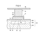
つまり、アクチュエータ基板32は、図4に示すように、最下層である基板層32Aと中間層であるスペーサ層32Bと最上層である薄板層32Cとの積層体であって、スペーサ層32Bのうち、アクチュエータ部34に対応する箇所に空所64が形成された一体構造体として把握することができる。基板層32Aは、補強用基板として機能するほか、配線用の基板としても機能するようになっている。なお、前記アクチュエータ基板32は、一体焼成であっても、各層を例えば接着剤等を用いて接合してもよい。   That is, as shown in FIG. 4, the actuator substrate 32 is a laminate of the lowermost substrate layer 32A, the intermediate spacer layer 32B, and the uppermost thin plate layer 32C. Thus, it can be grasped as an integral structure in which a void 64 is formed at a location corresponding to the actuator portion 34. The substrate layer 32A functions not only as a reinforcing substrate but also as a wiring substrate. The actuator substrate 32 may be integrally fired or each layer may be bonded using, for example, an adhesive.

基板層32A、スペーサ層32B及び薄板層32Cの構成材料としては、例えば、安定化酸化ジルコニウム、部分安定化酸化ジルコニウム、酸化アルミニウム、酸化マグネシウム、酸化チタン、スピネル及びムライト等の高耐熱性、高強度及び高靭性を兼ね備えるものが好適に採用される。なお、基板層32A、スペーサ層32B及び薄板層32Cは、全て同一材料としてもよく、それぞれ別の材料としてもよい。   As a constituent material of the substrate layer 32A, the spacer layer 32B, and the thin plate layer 32C, for example, high heat resistance and high strength such as stabilized zirconium oxide, partially stabilized zirconium oxide, aluminum oxide, magnesium oxide, titanium oxide, spinel and mullite. And what has high toughness is employ | adopted suitably. The substrate layer 32A, the spacer layer 32B, and the thin plate layer 32C may all be made of the same material or different materials.

そして、薄板層32Cの厚みとしては、アクチュエータ部34を大きく変位させるために、50μm以下とされ、好ましくは3〜20μm程度とされる。   The thickness of the thin plate layer 32C is set to 50 μm or less and preferably about 3 to 20 μm in order to greatly displace the actuator portion 34.

スペーサ層32Bは、アクチュエータ基板32に空所64を構成するものとして存在していればよく、その厚みは特に制限されるものではない。しかし一方で、空所64の利用目的に応じてその厚みを決定してもよく、その中でもアクチュエータ部34が機能する上で必要以上の厚みを有さず、薄い状態で構成されていることが好ましい。すなわち、スペーサ層32Bの厚みは、利用するアクチュエータ部34の変位の大きさ程度であることが好ましい。   The spacer layer 32 </ b> B only needs to be present as the void 64 in the actuator substrate 32, and the thickness thereof is not particularly limited. However, on the other hand, the thickness may be determined according to the purpose of use of the space 64, and among them, the actuator portion 34 does not have a thickness more than necessary to function, and is configured in a thin state. preferable. That is, the thickness of the spacer layer 32B is preferably about the magnitude of the displacement of the actuator portion 34 to be used.

このような構成により、薄肉の部分(振動部66の部分)の撓みが、その撓み方向に近接する基板層32Aにより制限され、意図しない外力の印加に対して、前記薄肉の部分の破壊を防止するという効果が得られる。なお、基板層32Aによる撓みの制限効果を利用して、アクチュエータ部34の変位を特定値に安定させることも可能である。   With such a configuration, the bending of the thin portion (vibrating portion 66 portion) is limited by the substrate layer 32A close to the bending direction, and the destruction of the thin portion is prevented when an unintended external force is applied. The effect of doing is obtained. In addition, it is also possible to stabilize the displacement of the actuator part 34 to a specific value by utilizing the effect of limiting the bending by the substrate layer 32A.

また、スペーサ層32Bを薄くすることで、アクチュエータ基板32自体の厚みが低減し、曲げ剛性を小さくすることができるため、例えばアクチュエータ基板32を別体に接着・固定するにあたって、相手方(例えば光導波板38や連結板40)に対し、自分自身(この場合、アクチュエータ基板32)の反り等が効果的に矯正され、接着・固定の信頼性の向上を図ることができる。   Further, since the thickness of the actuator substrate 32 itself can be reduced and the bending rigidity can be reduced by making the spacer layer 32B thin, for example, when the actuator substrate 32 is bonded and fixed separately, the other party (for example, optical waveguide) The warpage of the self (in this case, the actuator substrate 32) or the like is effectively corrected with respect to the plate 38 and the connecting plate 40), and the reliability of adhesion and fixation can be improved.

加えて、アクチュエータ基板32が全体として薄く構成されるため、アクチュエータ基板32を製造する際に、原材料の使用量を低減することができ、製造コストの観点からも有利な構造である。従って、スペーサ層32Bの具体的な厚みとしては、3〜50μmとすることが好ましく、中でも3〜20μmとすることが好ましい。   In addition, since the actuator substrate 32 is configured to be thin as a whole, the amount of raw materials used can be reduced when the actuator substrate 32 is manufactured, which is an advantageous structure from the viewpoint of manufacturing cost. Therefore, the specific thickness of the spacer layer 32B is preferably 3 to 50 μm, and more preferably 3 to 20 μm.

一方、基板層32Aの厚みとしては、上述したスペーサ層32Bを薄く構成することから、アクチュエータ基板32全体の補強目的として、50μm以上、好ましくは80〜300μm程度とされる。   On the other hand, the thickness of the substrate layer 32A is set to 50 μm or more, preferably about 80 to 300 μm for the purpose of reinforcing the entire actuator substrate 32 because the spacer layer 32B described above is formed thin.

ここで、アクチュエータ部34の具体例を図4に基づいて説明する。このアクチュエータ部34は、図4に示すように、振動部66と固定部68のほか、該振動部66上に直接形成された圧電/電歪層72と、該圧電/電歪層72の上面と下面に形成された一対の電極74a及び74bとからなるアクチュエータ本体75を有する。   Here, a specific example of the actuator unit 34 will be described with reference to FIG. As shown in FIG. 4, in addition to the vibrating portion 66 and the fixed portion 68, the actuator portion 34 includes a piezoelectric / electrostrictive layer 72 formed directly on the vibrating portion 66, and an upper surface of the piezoelectric / electrostrictive layer 72. And an actuator body 75 composed of a pair of electrodes 74a and 74b formed on the lower surface.

一対の電極74a及び74bは、図4に示すように、圧電/電歪層72に対して上下に形成した構造や片側だけに形成した構造でもよいし、圧電/電歪層72の上部のみに一対の電極74a及び74bを形成するようにしてもよい。   As shown in FIG. 4, the pair of electrodes 74 a and 74 b may have a structure formed above and below the piezoelectric / electrostrictive layer 72, a structure formed only on one side, or only on the upper part of the piezoelectric / electrostrictive layer 72. A pair of electrodes 74a and 74b may be formed.

一対の電極74a及び74bを圧電/電歪層72の上部のみに形成する場合、一対の電極74a及び74bの平面形状としては、多数のくし歯が相補的に対峙した形状のほか、特開平10−78549号公報や特開2001−324961号公報にも示されているように、渦巻き状や多枝形状等を採用してもよい。   When the pair of electrodes 74a and 74b are formed only on the upper part of the piezoelectric / electrostrictive layer 72, the planar shape of the pair of electrodes 74a and 74b is a shape in which a number of comb teeth complementarily face each other. As shown in Japanese Patent Application Publication No. -78549 and Japanese Patent Application Laid-Open No. 2001-324961, a spiral shape, a multi-branch shape, or the like may be employed.

また、一対の電極74a及び74bは、アルミニウム、チタン、クロム、鉄、コバルト、ニッケル、銅、亜鉛、ニオブ、モリブデン、ルテニウム、パラジウム、ロジウム、銀、スズ、タンタル、タングステン、イリジウム、白金、金、鉛等の各金属、あるいはこれらのうちの2種類以上を構成成分とする合金、また、これら金属単体及び合金に酸化アルミニウム、酸化チタン、酸化ジルコニウム、酸化セリウム、酸化銅等の金属酸化物を添加したもの、さらには金属単体及び合金に対して前述したアクチュエータ基板32の構成材料、及び/又は後述の圧電/電歪材料と同じ材料を分散させたサーメットとしたもの等の導電材料を用いることができる。   The pair of electrodes 74a and 74b are made of aluminum, titanium, chromium, iron, cobalt, nickel, copper, zinc, niobium, molybdenum, ruthenium, palladium, rhodium, silver, tin, tantalum, tungsten, iridium, platinum, gold, Each metal such as lead, or an alloy containing two or more of these as constituents, and metal oxides such as aluminum oxide, titanium oxide, zirconium oxide, cerium oxide, and copper oxide are added to these metals and alloys. In addition, a conductive material such as a cermet in which the same material as the constituent material of the actuator substrate 32 described above and / or the piezoelectric / electrostrictive material described later is dispersed is used for a single metal and an alloy. it can.

アクチュエータ基板32上に一対の電極74a及び74bを形成する方法としては、フォトリソグラフィ法、スクリーン印刷法、ディッピング法、塗布法、電気泳動法、イオンビーム法、スパッタリング法、真空蒸着法、イオンプレーティング法、化学気相成長(CVD)法、あるいはめっき等の膜形成法が挙げられる。   As a method of forming the pair of electrodes 74a and 74b on the actuator substrate 32, a photolithography method, a screen printing method, a dipping method, a coating method, an electrophoresis method, an ion beam method, a sputtering method, a vacuum deposition method, an ion plating method. And film formation methods such as plating, chemical vapor deposition (CVD), and plating.

圧電/電歪層72の構成材料の好適な例としては、ジルコン酸鉛、マンガンタングステン酸鉛、チタン酸ナトリウムビスマス、鉄酸ビスマス、ニオブ酸カリウムナトリウム、タンタル酸ストロンチウムビスマス、マグネシウムニオブ酸鉛、ニッケルニオブ酸鉛、亜鉛ニオブ酸鉛、マンガンニオブ酸鉛、マグネシウムタンタル酸鉛、ニッケルタンタル酸鉛、アンチモンスズ酸鉛、チタン酸鉛、チタン酸バリウム、銅タングステン酸バリウム、マグネシウムタングステン酸鉛、コバルトニオブ酸鉛、あるいはこれらのうちの2種以上からなる複合酸化物を挙げることができる。また、これらの圧電/電歪体材料には、ランタン、カルシウム、ストロンチウム、モリブデン、タングステン、バリウム、ニオブ、亜鉛、ニッケル、マンガン、セリウム、カドミウム、クロム、コバルト、アンチモン、鉄、イットリウム、タンタル、リチウム、ビスマス、スズ、銅等の酸化物が固溶されていてもよい。   Suitable examples of the constituent material of the piezoelectric / electrostrictive layer 72 include lead zirconate, lead manganese tungstate, sodium bismuth titanate, bismuth ferrate, potassium sodium niobate, strontium bismuth tantalate, lead magnesium niobate, nickel Lead niobate, lead zinc niobate, lead manganese niobate, lead magnesium tantalate, lead nickel tantalate, lead antimony stannate, lead titanate, barium titanate, barium copper tungstate, lead magnesium tungstate, cobalt niobate Examples thereof include lead and composite oxides composed of two or more of these. These piezoelectric / electrostrictive materials include lanthanum, calcium, strontium, molybdenum, tungsten, barium, niobium, zinc, nickel, manganese, cerium, cadmium, chromium, cobalt, antimony, iron, yttrium, tantalum, and lithium. Further, oxides such as bismuth, tin, and copper may be dissolved.

なお、圧電/電歪層72の代わりに反強誘電体層を用いてもよい。この場合、ジルコン酸鉛、ジルコン酸鉛及びスズ酸鉛の複合酸化物、ジルコン酸鉛、スズ酸鉛及びニオブ酸鉛の複合酸化物等を挙げることができる。これらの反強誘電体材料も、上記したような各元素が固溶されていてもよい。   Instead of the piezoelectric / electrostrictive layer 72, an antiferroelectric layer may be used. In this case, there may be mentioned lead zirconate, lead zirconate and lead stannate composite oxide, lead zirconate, lead stannate and lead niobate composite oxide, and the like. These antiferroelectric materials may also have the above-described elements dissolved therein.

また、前記材料等に、ビスマス酸リチウム、ゲルマン酸鉛等を添加した材料、例えばジルコン酸鉛、チタン酸鉛及びマグネシウムニオブ酸鉛の複合酸化物にビスマス酸リチウムないしゲルマン酸鉛を添加した材料は、圧電/電歪層72の低温焼成を実現しつつ高い材料特性を発現できるので好ましい。なお、低温焼成化はガラスの添加(例えば珪酸塩ガラス、硼酸塩ガラス、燐酸塩ガラス、ゲルマン酸塩ガラス、又はそれらの混合物)によっても実現させることができる。ただ、過剰な添加は、材料特性の劣化を招くため、要求特性に応じて添加量を決めることが望ましい。   Further, a material obtained by adding lithium bismutate, lead germanate, etc. to the above materials, for example, a material obtained by adding lithium bismutate or lead germanate to a composite oxide of lead zirconate, lead titanate and lead magnesium niobate The piezoelectric / electrostrictive layer 72 is preferable because it can exhibit high material properties while realizing low-temperature firing. Note that the low-temperature firing can be realized by addition of glass (for example, silicate glass, borate glass, phosphate glass, germanate glass, or a mixture thereof). However, excessive addition leads to deterioration of material characteristics, so it is desirable to determine the addition amount according to required characteristics.

ところで、図4に示すように、一対の電極74a及び74bとして、圧電/電歪層72の下面に下部電極74aを形成し、圧電/電歪層72の上面に上部電極74bを形成した場合においては、図2に示すように、アクチュエータ部34を空所64側に凸となるように一方向に屈曲変位させることも可能であり、その他、アクチュエータ部34を連結板40側に凸となるように、他方向に屈曲変位させることも可能である。   Incidentally, as shown in FIG. 4, in the case where the lower electrode 74a is formed on the lower surface of the piezoelectric / electrostrictive layer 72 and the upper electrode 74b is formed on the upper surface of the piezoelectric / electrostrictive layer 72 as a pair of electrodes 74a and 74b. As shown in FIG. 2, the actuator portion 34 can be bent and displaced in one direction so as to be convex toward the space 64, and the actuator portion 34 may be convex toward the connecting plate 40. It is also possible to bend and displace in the other direction.

ここで、空所64の開口幅(面積)は、アクチュエータ本体75の幅(面積)よりも大きいことが好ましいが、空所64の開口幅(面積)は、アクチュエータ本体75の幅(面積)と同等でもよいし、わずかに小さくてもよい。   Here, the opening width (area) of the space 64 is preferably larger than the width (area) of the actuator body 75, but the opening width (area) of the space 64 is equal to the width (area) of the actuator body 75. They may be the same or slightly smaller.

一方、変位伝達部39は、複数の変位伝達部材76を有し、1つのアクチュエータ部34に対して1つの変位伝達部材76が割り当てられて形成されている。変位伝達部材76は、アクチュエータ本体75の変位を上方に伝えるためのものであるが、例えば接着剤を用いることができる。フィラー含有接着剤を用いてもよい。   On the other hand, the displacement transmission part 39 has a plurality of displacement transmission members 76, and one displacement transmission member 76 is assigned to one actuator part 34. The displacement transmission member 76 is for transmitting the displacement of the actuator body 75 upward, and for example, an adhesive can be used. A filler-containing adhesive may be used.

もちろん、変位伝達部材76は、特に限定されるものではないが、熱可塑性樹脂、熱硬化性樹脂、光硬化性樹脂、吸湿硬化性樹脂、常温硬化性樹脂等を好適な例として挙げることができる。   Of course, the displacement transmission member 76 is not particularly limited, but a thermoplastic resin, a thermosetting resin, a photocurable resin, a moisture-absorbing curable resin, a room temperature curable resin, and the like can be given as suitable examples. .

具体的には、アクリル系樹脂、変性アクリル系樹脂、エポキシ樹脂、変性エポキシ樹脂、シリコーン樹脂、変性シリコーン樹脂、酢酸ビニル系樹脂、エチレン−酢酸ビニル共重合体系樹脂、ビニルブチラール系樹脂、シアノアクリレート系樹脂、ウレタン系樹脂、ポリイミド系樹脂、メタクリル系樹脂、変性メタクリル系樹脂、ポリオレフィン系樹脂、特殊シリコーン変性ポリマー、ポリカーボネート系樹脂、天然ゴム、合成ゴム等が例示される。   Specifically, acrylic resins, modified acrylic resins, epoxy resins, modified epoxy resins, silicone resins, modified silicone resins, vinyl acetate resins, ethylene-vinyl acetate copolymer resins, vinyl butyral resins, cyanoacrylate resins Examples thereof include resins, urethane resins, polyimide resins, methacrylic resins, modified methacrylic resins, polyolefin resins, special silicone modified polymers, polycarbonate resins, natural rubber, and synthetic rubber.

特に、ビニルブチラール系樹脂、アクリル系樹脂、変性アクリル系樹脂、エポキシ樹脂、変性エポキシ樹脂、あるいはこれらの2種以上の混合物は接着強度に優れるので好適であり、とりわけ、エポキシ樹脂、変性エポキシ樹脂、あるいはこれらの混合物が好適である。   In particular, a vinyl butyral resin, an acrylic resin, a modified acrylic resin, an epoxy resin, a modified epoxy resin, or a mixture of two or more of these is preferable because of its excellent adhesive strength, and in particular, an epoxy resin, a modified epoxy resin, Alternatively, a mixture of these is preferred.

また、変位伝達部39は、複数の変位伝達部材76上に共通して接続された1つの連結板40を有する。すなわち、連結板40と変位伝達部材76の端面は、固着(接合)されていてもよいし、単に接触していてもよい。従って、以下の説明は、これら「固着」及び「接触」を包含する意味で「接続」という文言を使用する。つまり、アクチュエータ部34と連結板40は変位伝達部材76を介して接続されることになる。   Moreover, the displacement transmission part 39 has the one connection board 40 connected in common on the some displacement transmission member 76. FIG. That is, the connecting plate 40 and the end face of the displacement transmission member 76 may be fixed (joined) or may simply be in contact with each other. Therefore, in the following description, the term “connection” is used to include these “adhesion” and “contact”. That is, the actuator unit 34 and the connecting plate 40 are connected via the displacement transmission member 76.

また、この第1の実施の形態では、アクチュエータ基板32と連結板40との間に第1のスペーサ42が形成され、連結板40と光導波板38との間に第2のスペーサ44が形成されている。   In the first embodiment, the first spacer 42 is formed between the actuator substrate 32 and the connecting plate 40, and the second spacer 44 is formed between the connecting plate 40 and the optical waveguide plate 38. Has been.

連結板40は、変位不良のアクチュエータ部34(欠陥アクチュエータ部)があった場合でも、連結板40に接続された正常のアクチュエータ部34の変位によって、前記欠陥アクチュエータ部34の変位を補償するために、最適な剛性が得られるような材質、厚みに選定されている。   The connecting plate 40 compensates for the displacement of the defective actuator portion 34 by the displacement of the normal actuator portion 34 connected to the connecting plate 40 even when there is an actuator portion 34 (defective actuator portion) having a poor displacement. The material and thickness are selected so that optimum rigidity can be obtained.

すなわち、連結板40は、金属、セラミックス、ガラス、有機樹脂等が利用でき、上記機能を満たすものなら、特に限定されるものではない。一例を挙げれば、SUS304(ヤング率:193GPa、線膨張係数:17.3×10⁻⁶/℃)、SUS403(ヤング率:200GPa、線膨張係数:10.4×10-6/℃)、酸化ジルコニウム(ヤング率:245.2GPa、線膨張係数:9.2×10-6/℃)、ガラス(例えばコーニング0211、ヤング率:74.4GPa、線膨張係数:7.38×10-6/℃)等が好ましく用いられる。この実施の形態では、SUS板を用いた。この場合、SUS板の厚みとしては、好ましくは10μm〜300μmである。 That is, the connecting plate 40 is not particularly limited as long as it can use metal, ceramics, glass, organic resin, or the like and satisfies the above functions. As an example, SUS304 (Young's modulus: 193 GPa, linear expansion coefficient: 17.3 × 10 −6 / ° C.), SUS403 (Young's modulus: 200 GPa, linear expansion coefficient: 10.4 × 10 −6 / ° C.), oxidation Zirconium (Young's modulus: 245.2 GPa, linear expansion coefficient: 9.2 × 10 −6 / ° C.), glass (for example, Corning 0211, Young's modulus: 74.4 GPa, linear expansion coefficient: 7.38 × 10 −6 / ° C. Etc.) are preferably used. In this embodiment, a SUS plate is used. In this case, the thickness of the SUS plate is preferably 10 μm to 300 μm.

第1及び第2のスペーサ42及び44の構成材料としては、熱、圧力に対して変形しないものが好ましい。例えばエポキシ樹脂等の熱硬化性樹脂や、光硬化性樹脂、吸湿硬化性樹脂、常温硬化性樹脂等を硬化させたもの等が挙げられる。   The constituent material of the first and second spacers 42 and 44 is preferably one that does not deform with respect to heat and pressure. For example, a thermosetting resin such as an epoxy resin, a photo-curing resin, a moisture curable resin, a room temperature curable resin, or the like is cured.

もちろん、第1及び第2のスペーサ42及び44にフィラーを含有させるようにしてもよい。フィラーを含有しない場合と比して硬度が高く、かつ耐熱性や強度、寸法安定性が高い。また、フィラーが含有されていないスペーサに比して、照明装置10Aの内部温度上昇に伴う変形量が著しく小さい。換言すれば、フィラーを含有させることによって、樹脂硬化物の硬度や耐熱性、強度を向上させることができ、かつ、熱による膨張・収縮量を著しく減少させることができる。   Of course, the first and second spacers 42 and 44 may contain a filler. Compared with the case where no filler is contained, the hardness is high, and the heat resistance, strength and dimensional stability are high. In addition, the amount of deformation associated with a rise in the internal temperature of the lighting device 10A is significantly smaller than a spacer that does not contain a filler. In other words, the inclusion of the filler can improve the hardness, heat resistance, and strength of the cured resin, and can significantly reduce the amount of expansion / contraction due to heat.

そして、この第1の実施の形態に係る表示装置に用いられる照明装置10Aにおいては、連結板40の上面全面に光反射層300が形成され、第2のスペーサ44と光導波板38との間に光反射層302が形成され、光反射層300の上面のうち、各発光区画50に対応した位置にそれぞれ1つの光散乱層80あるいは複数の光散乱層80が形成されている。   In the illuminating device 10A used in the display device according to the first embodiment, the light reflecting layer 300 is formed on the entire upper surface of the connecting plate 40, and the space between the second spacer 44 and the optical waveguide plate 38 is formed. The light reflection layer 302 is formed, and one light scattering layer 80 or a plurality of light scattering layers 80 are formed at positions corresponding to the respective light emitting sections 50 on the upper surface of the light reflection layer 300.

光散乱層80の構成材料としては、例えば白色を含む有色透明材料、有色半透明材料を使用することができる。透明材料であって、気孔等を有する異種材料を含むものであれば使用可能である。好ましくは、異なる2相以上の相を有する材料等であり、例えば樹脂に粉末を混ぜた物が挙げられる。   As a constituent material of the light scattering layer 80, for example, a colored transparent material including white and a colored translucent material can be used. Any transparent material may be used as long as it includes a different material having pores or the like. Preferably, it is a material having two or more different phases, for example, a material in which a powder is mixed with a resin.

樹脂としては、アクリル樹脂のほか、ポリカーボネート系、スチレン系、エポキシ系、シリコーン系、ポリオレフィン系等、各種有機樹脂が挙げられるが、ゴムやガラス等でもよい。   As the resin, in addition to acrylic resin, various organic resins such as polycarbonate, styrene, epoxy, silicone, and polyolefin can be used, but rubber, glass, and the like may be used.

粉末としては、前記樹脂(各種組み合わせを含む)とは別の物性を有するセラミック粉末、樹脂等、各種挙げられる。粉末ではないが、気泡を形成してもよい。   Examples of the powder include various ceramic powders and resins having physical properties different from those of the resin (including various combinations). Although not a powder, bubbles may be formed.

さらに好ましくは、前記異なる2相以上の相において、各材料の屈折率差を大きくすることが、光散乱層の散乱効率を上げ、その厚みを薄くできる点で有利である。   More preferably, increasing the refractive index difference between the materials in the two or more different phases is advantageous in that the scattering efficiency of the light scattering layer can be increased and the thickness thereof can be reduced.

具体的には、粉末として、高屈折率材料のセラミック粉末、例えばTiO2系、ZrO2系、Ta25系、CeO2系、NbO5系、PbO系等を用いることが好ましい。屈折率は2.0以上が好ましく、2.5以上であればさらに好ましい。また、樹脂としては、前記有機樹脂の中でも、屈折率が1.7以下のものがより好ましく、1.5のものがさらに好ましい。 Specifically, it is preferable to use ceramic powder of a high refractive index material such as TiO 2 , ZrO 2 , Ta 2 O 5 , CeO 2 , NbO 5 , PbO and the like as the powder. The refractive index is preferably 2.0 or more, and more preferably 2.5 or more. As the resin, among the organic resins, those having a refractive index of 1.7 or less are more preferable, and those having a refractive index of 1.5 are more preferable.

光散乱層80の厚みは3μm〜50μmが好ましく、さらに好ましくは5μm〜15μmである。   The thickness of the light scattering layer 80 is preferably 3 μm to 50 μm, more preferably 5 μm to 15 μm.

光反射層300の構成材料としては、金属膜が好ましく用いられ、その形成法は、蒸着法のほか、金属箔を貼り付ける方法でもよい。金属膜としては、特に、Ag、Alが好ましい。反射率が高く、適度な柔軟性を有するからである。光反射層300の厚みは、0.001μm〜100μmが好ましく、さらに好ましくは0.1μm〜20μmである。   As a constituent material of the light reflecting layer 300, a metal film is preferably used, and the formation method thereof may be a vapor deposition method or a method of attaching a metal foil. As the metal film, Ag and Al are particularly preferable. This is because it has high reflectivity and moderate flexibility. The thickness of the light reflecting layer 300 is preferably 0.001 μm to 100 μm, and more preferably 0.1 μm to 20 μm.

光反射層302の構成材料としては、光反射層300の構成材料と同様の材料を用いることができる。但し、光反射層302は、適度な柔軟性が必要だが、上述した光反射層300は、剛性を有することが好ましい。光反射層302の厚みは、0.001μm〜1000μmが好ましく、さらに好ましくは0.1μm〜100μmである。   As the constituent material of the light reflecting layer 302, the same material as the constituent material of the light reflecting layer 300 can be used. However, the light reflecting layer 302 needs to have appropriate flexibility, but the light reflecting layer 300 described above preferably has rigidity. The thickness of the light reflecting layer 302 is preferably 0.001 μm to 1000 μm, more preferably 0.1 μm to 100 μm.

なお、アクチュエータ基板32への電極74a及び74b、圧電/電歪層72、第1及び第2のスペーサ42及び44等の膜の形成、並びに第2のスペーサ44上への光反射層302の形成、連結板40への光反射層300及び光散乱層80等の形成は、特に制限はなく、公知の各種の膜形成法を適用することができる。   Note that the electrodes 74 a and 74 b, the piezoelectric / electrostrictive layer 72, the first and second spacers 42 and 44, etc. are formed on the actuator substrate 32, and the light reflecting layer 302 is formed on the second spacer 44. The formation of the light reflecting layer 300 and the light scattering layer 80 on the connecting plate 40 is not particularly limited, and various known film forming methods can be applied.

例えばアクチュエータ基板32や連結板40の面上に成膜する方法としては、チップ状、フィルム状の膜を直接貼り付けるフィルム貼着法ほか、膜の原材料となる粉末、ペースト、液体、気体、イオン等を、スクリーン印刷法、フォトリソグラフィ法、スプレー・ディッピング法、塗布等の厚膜形成法や、イオンビーム法、スパッタリング法、真空蒸着法、イオンプレーティング法、化学気相成長(CVD)法、めっき等の薄膜形成法等が挙げられる。   For example, as a method of forming a film on the surface of the actuator substrate 32 or the connecting plate 40, a film sticking method in which a chip-like film or a film-like film is directly attached, or a powder, paste, liquid, gas, ion, which is a raw material of the film Etc., screen printing method, photolithography method, spray dipping method, thick film forming method such as coating, ion beam method, sputtering method, vacuum deposition method, ion plating method, chemical vapor deposition (CVD) method, Examples include a thin film forming method such as plating.

ここで、照明装置10Aの動作を図2及び図4を参照しながら簡単に説明する。先ず、光導波板38の例えば端部から光33が導入される。この場合、光散乱層80が光導波板38に接触していない状態で、光導波板38の屈折率の大きさを調節することにより、全ての光33を光導波板38の主面及び背面において透過することなく内部で全反射させるようにする。光導波板38の屈折率としては、1.3〜1.8が望ましく、1.4〜1.7がより望ましい。   Here, operation | movement of 10 A of illuminating devices is demonstrated easily, referring FIG.2 and FIG.4. First, light 33 is introduced from, for example, an end of the optical waveguide plate 38. In this case, by adjusting the refractive index of the optical waveguide plate 38 in a state where the light scattering layer 80 is not in contact with the optical waveguide plate 38, all the light 33 is transmitted to the main surface and the back surface of the optical waveguide plate 38. So that it is totally reflected inside without being transmitted. The refractive index of the optical waveguide plate 38 is desirably 1.3 to 1.8, and more desirably 1.4 to 1.7.

この例においては、アクチュエータ部34の自然状態において、光散乱層80の端面が光導波板38の背面に対して導入光33の波長以下の距離で接触しているため、導入光33は、光散乱層80の表面で反射し、散乱光82となる。この散乱光82は、一部は再度光導波板38の中で反射するが、散乱光82の大部分は光導波板38で反射されることなく、光導波板38の主面を透過することになる。これによって、全てのアクチュエータ部34がオン状態となり、そのオン状態が光の出射(発光)というかたちで具現され、しかも、その発光色は光散乱層80の色に対応したものとなる。この場合、全ての発光区画50に対応するアクチュエータ部34がオン状態となっているため、照明装置10Aにおける光導波板38の主面からは例えば白色発光が出射されることになる。   In this example, since the end surface of the light scattering layer 80 is in contact with the back surface of the optical waveguide plate 38 at a distance equal to or smaller than the wavelength of the introduction light 33 in the natural state of the actuator unit 34, The light is reflected from the surface of the scattering layer 80 and becomes scattered light 82. A part of the scattered light 82 is reflected again in the optical waveguide plate 38, but most of the scattered light 82 is not reflected by the optical waveguide plate 38 and passes through the main surface of the optical waveguide plate 38. become. As a result, all the actuator portions 34 are turned on, and the on state is embodied in the form of light emission (light emission), and the emission color corresponds to the color of the light scattering layer 80. In this case, since the actuator units 34 corresponding to all the light emitting sections 50 are in the ON state, for example, white light emission is emitted from the main surface of the optical waveguide plate 38 in the illumination device 10A.

また、さらには、アクチュエータ部34の電極74bと電極74aとの間に低レベル電圧(例えば−10V)が駆動電圧として印加されることにより、光散乱層80の端面が光導波板38の背面に対して押し付けられる状態で接触し、より確実なオン状態を作り出すことが可能となり、安定した発光が可能となる。   Further, a low level voltage (for example, −10 V) is applied as a drive voltage between the electrode 74 b and the electrode 74 a of the actuator unit 34, so that the end surface of the light scattering layer 80 is placed on the back surface of the optical waveguide plate 38. On the other hand, it is possible to create a more reliable ON state by touching in a pressed state, and stable light emission is possible.

この状態から、ある発光区画50に対応する6つのアクチュエータ部34の電極74bと電極74aとの間に高レベルの駆動電圧(例えば50V)が印加されると、当該発光区画50に対応する6つのアクチュエータ部34が図2に示すように、空所64側に凸となるように屈曲変位、すなわち、下方に屈曲変位することから、この駆動変位が変位伝達部材76及び連結板40を通じて光散乱層80に伝わり、これによって、光散乱層80の端面が光導波板38から離隔し、当該発光区画50に対応するアクチュエータ部34がオフ状態となり、そのオフ状態が消光というかたちで具現される。   From this state, when a high level drive voltage (for example, 50 V) is applied between the electrodes 74b and 74a of the six actuator units 34 corresponding to a certain light emitting section 50, the six corresponding to the light emitting section 50 As shown in FIG. 2, the actuator portion 34 is bent and displaced so as to protrude toward the space 64, that is, bent downward, so that the driving displacement is transmitted through the displacement transmitting member 76 and the connecting plate 40 to the light scattering layer. 80, whereby the end face of the light scattering layer 80 is separated from the optical waveguide plate 38, the actuator part 34 corresponding to the light emitting section 50 is turned off, and the off state is embodied in the form of quenching.

つまり、この照明装置10Aは、光散乱層80の光導波板38への接触の有無により、光導波板38の主面における光の発光(散乱光82)の有無を制御することができる。   That is, the illumination device 10 </ b> A can control the presence / absence of light emission (scattered light 82) on the main surface of the optical waveguide plate 38 based on the presence / absence of contact of the light scattering layer 80 with the optical waveguide plate 38.

このように、第1の実施の形態に係る表示装置に用いられる照明装置10Aにおいては、全発光区画50の光散乱層80を光導波板38に接触させることで、光導波板38の主面(光が出射する面)全面から光82が出射されることになる。このとき、液晶パネル12の正面輝度の向上を図るため、また、偏光板による光の損失を最小限にするため、図1に示すように、照明装置10Aと液晶パネル12との間に、光学シート304(二点鎖線で示す)を備える構成とする。   Thus, in the illuminating device 10A used in the display device according to the first embodiment, the main surface of the optical waveguide plate 38 is obtained by bringing the light scattering layer 80 of all the light emitting sections 50 into contact with the optical waveguide plate 38. (Surface on which light is emitted) The light 82 is emitted from the entire surface. At this time, in order to improve the front luminance of the liquid crystal panel 12 and to minimize the light loss due to the polarizing plate, as shown in FIG. A sheet 304 (indicated by a two-dot chain line) is provided.

例えば光学シートとして、液晶パネル12の正面方向に光を集光して正面輝度を向上させるプリズムシートや、偏光板による損失を最小限にする反射型偏光フィルムがあり、これらは組み合わせても使用される。ここでは、プリズムシートとして住友スリーエム社製のBEFII90/50を、反射型偏光フィルムとして住友スリーエム社製のDBEF−Dを用いた。プリズムシートは、背面(ここでは照明装置10A)からの光を正面方向に集光して透過するが、プリズムの全反射条件により約半分の光は背面へ戻されてしまう。また、反射型偏光フィルムは、例えば偏光成分のP波だけを透過し、S波は反射して背面へ戻されてしまう。いずれの光学シートもそれら背面に戻された光、つまり再帰光がかなり多く、このままでは光学シートを用いることで光の利用効率が低下してしまう。しかし、通常の照明装置は、底部に配置された反射シートにより光が反射され、その反射された光が再利用されるため、光学シートを用いることで光の利用効率が向上する。   For example, as an optical sheet, there are a prism sheet that condenses light in the front direction of the liquid crystal panel 12 to improve the front luminance, and a reflective polarizing film that minimizes the loss due to the polarizing plate. The Here, BEFII90 / 50 manufactured by Sumitomo 3M was used as the prism sheet, and DBEF-D manufactured by Sumitomo 3M was used as the reflective polarizing film. The prism sheet condenses and transmits light from the back surface (in this case, the illumination device 10A) in the front direction, but about half of the light is returned to the back surface due to the total reflection condition of the prism. In addition, the reflective polarizing film transmits, for example, only the P wave of the polarization component, and the S wave is reflected and returned to the back surface. All of the optical sheets have a large amount of light returned to their back surface, that is, recursive light, and the light use efficiency is lowered by using the optical sheet as it is. However, in a normal lighting device, light is reflected by a reflection sheet disposed at the bottom, and the reflected light is reused. Therefore, the use efficiency of light is improved by using an optical sheet.

この第1の実施の形態において、連結板40の上面全面に光反射層300を形成し、さらに、第2のスペーサ44と光導波板との間に光反射層302を形成するようにしているため、通常の照明装置と同様に、前記再帰光も前方に反射させることができ、光学シート304により光の利用効率が向上し、光学シート304の効果を引き出すことが可能となる。   In the first embodiment, the light reflecting layer 300 is formed on the entire upper surface of the coupling plate 40, and the light reflecting layer 302 is further formed between the second spacer 44 and the optical waveguide plate. Therefore, like the normal lighting device, the retroreflected light can also be reflected forward, and the optical sheet 304 can improve the use efficiency of light, and the effect of the optical sheet 304 can be brought out.

すなわち、この第1の実施の形態においては、光導波板38の主面(光の出射面)から効率よく光82を出射させることができる。   That is, in the first embodiment, the light 82 can be efficiently emitted from the main surface (light emission surface) of the optical waveguide plate 38.

また、駆動部36によるアクチュエータ部34に対する選択的な変位駆動によって、一部の発光区画50の光散乱層80を光導波板38に接触させることで、光導波板38の主面のうち、一部から光82が出射されることになる。すなわち、光導波板38の主面の一部から選択的に光82を出射させることができる。しかも、駆動部36によるアクチュエータ部34に対する選択的な変位駆動を一定の周期(例えば液晶パネル12の垂直走査信号の周期等)に従って制御することで光82の出射領域を段階的に移動させることができる。   Further, by selectively driving the actuator unit 34 with respect to the actuator unit 34 by bringing the light scattering layer 80 of some of the light-emitting sections 50 into contact with the optical waveguide plate 38, one of the main surfaces of the optical waveguide plate 38. Light 82 is emitted from the portion. That is, the light 82 can be selectively emitted from a part of the main surface of the optical waveguide plate 38. In addition, by selectively driving the displacement of the actuator unit 34 by the driving unit 36 according to a certain period (for example, the period of the vertical scanning signal of the liquid crystal panel 12), the emission region of the light 82 can be moved stepwise. it can.

例えば図5に示すように、m個の発光区画501、502、503・・・50mを垂直方向に並べ、垂直走査信号の1周期の期間をTvとしたとき、各発光区画は、(Tv/m)の期間だけ発光タイミングをずらしながら発光するように制御する。つまり、発光区画501から光が出射された後、(Tv/m)の期間の後に発光区画502から光が出射され、発光区画502から光が出射された後、(Tv/m)の期間の後に発光区画503から光が出射され、以下同様に発光するタイミングをずらしながら、発光区画50mから光が出射される。各発光区画では、光が出射した後、オフ(消光)される。発光区画50mから光が出射された後は、(Tv/m)の期間の後に発光区画501からの光出射へと繰り返される。また、各発光区画での光出射の時間が同じ場合、発光区画が順次移り変わっていく。さらに、その光出射期間が(Tv/m)の期間より短い時間であれば、同時に光出射する発光区画は存在しない。具体的には、映像信号の垂直走査信号が60Hz(ヘルツ)の場合、垂直走査信号の1周期の期間Tvは(1/60)秒となり、発光区画が4個(つまり、mが4)の場合、各発光区画間での光出射のタイミングのずれは(1/240)秒の期間となる。このときの光出射のタイミングチャートを図6に示す。横軸は時間で、縦軸は発光区画ごとの光出射強度である。1つ目の発光区画は例えば時間0から光出射を開始し、2つ目の発光区画は1つ目の発光区画から(1/240)秒の期間の後に光出射を開始し、3つ目の発光区画は、2つ目の発光区画から(1/240)秒の期間の後に光出射を開始し、4つ目の発光区画は、3つ目の発光区画から(1/240)秒の期間の後に光出射を開始する。それぞれの発光区画の光出射の期間は任意であるが、例えば(1/240)秒であると、図6に示すように、同時に光出射する発光区画は存在せず、光出射する発光区画が順次移り変わっている様子が明らかである。また、ある発光区画を注目すると、Tvの周期、つまり、(1/60)秒で光出射している。なお、光出射時間は、各発光区画の光出射のタイミングのずれと同じである必要はなく、これより長くても短くてもよい。但し、短い場合には、どの発光区画からも光が出射されていない時間が存在するため、光の利用効率は低下してしまい、長い場合には、消光時間(光出射していない時間)が短くなるため、擬似的なインパルス発生の効果が小さくなる。 For example, as shown in FIG. 5, when m light emitting sections 50 1 , 50 2 , 50 3 ... 50 m are arranged in the vertical direction and the period of one cycle of the vertical scanning signal is Tv, each light emitting section is Control is performed so that light is emitted while shifting the light emission timing only during the period of (Tv / m). That is, after light is emitted from the light emitting section 50 1 , light is emitted from the light emitting section 50 2 after a period of (Tv / m), and after light is emitted from the light emitting section 50 2 , (Tv / m) the light emitted from the light emitting section 50 3 after a period, while shifting the timing of similarly emitting less, light is emitted from the light emitting section 50 m. Each light emitting section is turned off (quenched) after light is emitted. After the light is emitted from the light emitting section 50m, the light emission from the light emitting section 50 1 is repeated after the period of (Tv / m). Further, when the light emission times in the respective light emitting sections are the same, the light emitting sections are sequentially changed. Furthermore, if the light emission period is shorter than the period (Tv / m), there is no light emitting section that emits light at the same time. Specifically, when the vertical scanning signal of the video signal is 60 Hz (Hertz), the period Tv of one cycle of the vertical scanning signal is (1/60) seconds, and there are four light emitting sections (that is, m is 4). In this case, the deviation of the light emission timing between the light emitting sections is a period of (1/240) seconds. A timing chart of light emission at this time is shown in FIG. The horizontal axis represents time, and the vertical axis represents the light emission intensity for each light emitting section. For example, the first light-emitting section starts light emission from time 0, and the second light-emitting section starts light emission after a period of (1/240) seconds from the first light-emitting section. The light emitting section starts emitting light after a period of (1/240) second from the second light emitting section, and the fourth light emitting section is (1/240) second from the third light emitting section. Light emission starts after the period. Although the light emission period of each light emitting section is arbitrary, for example (1/240) seconds, as shown in FIG. 6, there is no light emitting section that emits light at the same time, and there is no light emitting section that emits light. It is clear that the situation is changing sequentially. Further, when attention is paid to a certain light emitting section, light is emitted in a cycle of Tv, that is, (1/60) second. The light emission time does not have to be the same as the deviation of the light emission timing of each light emitting section, and may be longer or shorter. However, in the case where the light is short, there is a time during which no light is emitted from any light emitting section, so that the light use efficiency is reduced. In the case where the light is long, the extinction time (time during which light is not emitted) is reduced. Since it becomes shorter, the effect of pseudo impulse generation is reduced.

次に、各発光区画の光出射状態と液晶パネル12の駆動状態を図7に示す。図7の横軸は時間で、縦軸は照明装置10Aのある発光区画(例えば501)の光出射強度及び液晶パネル12の透過率を示している。液晶パネル12は上記のように映像信号の垂直走査信号の周期が60Hzの場合、ある画素に注目すれば、(1/60)秒で画像が書き換えられ、例えば1周期ごとに透過状態と消光状態が変わる場合、液晶パネル12の駆動は、図7に示すように、消光状態から緩やかに透過状態へ遷移し、次の周期で透過状態から消光状態へ緩やかに遷移する。液晶の応答は1周期ごとに透過状態と消光状態を切り替えるのに、垂直走査信号が60Hzの場合、約16.6msec以下での応答を必要とするが、実際には、図7に示すように、緩やかな応答をする。そのため、発光区画の光出射は、液晶が応答する1周期の後半の期間で行うことが望ましい。この発光区画からの光出射の様子を図7の斜線で示した矩形で表す。このとき、1周期目では、液晶が透過状態で光出射をするために明状態、2周期目では、液晶が消光状態で光出射をするために暗状態となる。この擬似的なインパルスの発生により、前述の残像感が軽減され、また、液晶の応答の遅さに起因する階調特性の劣化が低減されることになる。つまり、液晶の応答がほぼ終了した期間での光出射となるので、透過率の遷移する期間の表示がされないため、適切な階調(表示レベル)が表示可能となる。 Next, the light emission state of each light emitting section and the driving state of the liquid crystal panel 12 are shown in FIG. In FIG. 7, the horizontal axis represents time, and the vertical axis represents the light emission intensity and the transmittance of the liquid crystal panel 12 in a light emitting section (for example, 50 1 ) in which the illumination device 10 </ b> A is provided. As described above, when the period of the vertical scanning signal of the video signal is 60 Hz, the liquid crystal panel 12 rewrites the image in (1/60) seconds if attention is paid to a certain pixel. For example, the transmission state and the extinction state every period. 7 changes, the driving of the liquid crystal panel 12 gradually changes from the extinction state to the transmission state, and then gradually changes from the transmission state to the extinction state in the next cycle. As for the response of the liquid crystal, when the vertical scanning signal is 60 Hz, the response in about 16.6 msec or less is required to switch between the transmission state and the extinction state every cycle, but actually, as shown in FIG. , Make a slow response. Therefore, it is desirable that the light emission of the light emitting section is performed in the latter half of one cycle in which the liquid crystal responds. The state of light emission from the light emitting section is represented by a rectangle shown by hatching in FIG. At this time, in the first period, the liquid crystal emits light in a transmissive state, and in the second period, the liquid crystal enters a dark state in order to emit light in an extinguished state. Due to the generation of the pseudo impulse, the above-mentioned afterimage feeling is reduced, and the deterioration of the gradation characteristics due to the slow response of the liquid crystal is reduced. That is, since light is emitted during the period when the response of the liquid crystal is almost finished, the period during which the transmittance transitions is not displayed, so that an appropriate gradation (display level) can be displayed.

また、この第1の実施の形態では、第2のスペーサ44と光導波板38との間に光反射層302を形成するようにしている。発光区画50の境界部分においては、光散乱層80が接触しないため、輝度が低下するおそれがあるが、第2のスペーサ44上に光反射層302を形成することで、光導波板38に導入された光33を第2のスペーサ44上で散乱させることができ、発光区画50の境界部分での輝度低下を抑えることができる。   In the first embodiment, the light reflecting layer 302 is formed between the second spacer 44 and the optical waveguide plate 38. Since the light scattering layer 80 does not come into contact with the boundary portion of the light emitting section 50, there is a possibility that the luminance may be reduced. The scattered light 33 can be scattered on the second spacer 44, and a decrease in luminance at the boundary portion of the light emitting section 50 can be suppressed.

ところで、照明装置10Aの薄型化を図るために、光散乱層80の厚みを薄くすることが考えられるが、該光散乱層80を薄くすると、光散乱層80に入射した光が該光散乱層80を通過し、発光として寄与しなくなるおそれがある。しかし、光散乱層80の下層に光反射層300を形成することで、該光散乱層80を通過した光を反射させることができ、光散乱層80を薄くすることによる輝度低下を抑えることができる。   By the way, in order to reduce the thickness of the lighting device 10A, it is conceivable to reduce the thickness of the light scattering layer 80. However, if the light scattering layer 80 is thinned, light incident on the light scattering layer 80 is converted into the light scattering layer 80. There is a possibility that it will not contribute as light emission. However, by forming the light reflection layer 300 under the light scattering layer 80, the light that has passed through the light scattering layer 80 can be reflected, and the reduction in luminance due to the thin light scattering layer 80 can be suppressed. it can.

また、1つのアクチュエータ部34に対して1つの変位伝達部材76を割り当てて形成するようにしたので、この第1の実施の形態のように、1つの発光区画50に複数のアクチュエータ部34が存在する場合、不良なアクチュエータ部34が存在していても、正常なアクチュエータ部34で変位を補償することができ、歩留まりを向上させることができる。   Further, since one displacement transmitting member 76 is assigned to one actuator portion 34 and formed, a plurality of actuator portions 34 exist in one light emitting section 50 as in the first embodiment. In this case, even if there is a defective actuator portion 34, the displacement can be compensated for by the normal actuator portion 34, and the yield can be improved.

このように、第1の実施の形態に係る表示装置に用いられる照明装置10Aは、液晶パネル12全面に対して光照射することに加えて、液晶パネル12の一部だけに選択的に光を照射したり、液晶パネル12での垂直走査信号の周期に合わせて光の照射領域を段階的に移動させるようにしたりすることができ、通常のホールド型表示に加え、擬似的なインパルス型表示が可能となり、残像感を軽減した表示装置を実現することができる。   As described above, the illumination device 10A used in the display device according to the first embodiment selectively emits light to only a part of the liquid crystal panel 12 in addition to irradiating the entire surface of the liquid crystal panel 12 with light. It is possible to irradiate or move the light irradiation area stepwise in accordance with the period of the vertical scanning signal on the liquid crystal panel 12, and in addition to the normal hold type display, a pseudo impulse type display is provided. Thus, a display device with reduced afterimage can be realized.

上述では、第1の実施の形態に係る表示装置に用いられる照明装置10Aの主要な構成部材の材料について説明したが、その他の構成部材(アクチュエータ基板32、光導波板38等)の材料について以下に説明する。   In the above description, the materials of the main constituent members of the illumination device 10A used in the display device according to the first embodiment have been described. The materials of the other constituent members (the actuator substrate 32, the optical waveguide plate 38, and the like) are described below. Explained.

先ず、光導波板38に入射される光33の光源としては、白熱電球、重水素放電ランプ、蛍光ランプ、水銀ランプ、メタルハライドランプ、ハロゲンランプ、キセノンランプ、トリチウムランプ、発光ダイオード、レーザ、プラズマ光源、熱陰極管、冷陰極管等が用いられる。   First, as a light source of the light 33 incident on the optical waveguide plate 38, an incandescent bulb, a deuterium discharge lamp, a fluorescent lamp, a mercury lamp, a metal halide lamp, a halogen lamp, a xenon lamp, a tritium lamp, a light emitting diode, a laser, a plasma light source. A hot cathode tube, a cold cathode tube, or the like is used.

振動部66は、高耐熱性材料であることが好ましい。その理由は、アクチュエータ部34を有機接着剤等の耐熱性に劣る材料を用いずに、固定部68によって直接振動部66を支持させる構造とする場合、少なくとも圧電/電歪層72の形成時に、振動部66が変質しないようにするため、振動部66は、高耐熱性材料であることが好ましい。   The vibrating portion 66 is preferably a high heat resistant material. The reason is that when the actuator part 34 is structured to directly support the vibration part 66 by the fixing part 68 without using a material having poor heat resistance such as an organic adhesive, at least when the piezoelectric / electrostrictive layer 72 is formed, In order to prevent the vibration part 66 from being altered, the vibration part 66 is preferably made of a high heat resistant material.

また、振動部66は、アクチュエータ基板32上に形成される一対の電極74a及び74bにおける一方の電極74aに通じる配線(例えば行選択線)と他方の電極74bに通じる配線(例えば信号線)との電気的な分離を行うために、電気絶縁材料であることが好ましい。   The vibrating portion 66 includes a wiring (for example, a row selection line) that communicates with one electrode 74a of the pair of electrodes 74a and 74b formed on the actuator substrate 32 and a wiring (for example, a signal line) that communicates with the other electrode 74b. In order to perform electrical separation, an electrically insulating material is preferable.

従って、振動部66は、高耐熱性の金属あるいはその金属表面をガラス等のセラミック材料で被覆したホーロー等の材料であってもよいが、セラミックスが最適である。   Therefore, the vibration part 66 may be a high heat-resistant metal or a material such as enamel whose metal surface is coated with a ceramic material such as glass, but ceramic is optimal.

振動部66を構成するセラミックスとしては、例えば安定化された酸化ジルコニウム、酸化アルミニウム、酸化マグネシウム、酸化チタン、スピネル、ムライト、窒化アルミニウム、窒化珪素、ガラス、これらの混合物等を用いることができる。安定化された酸化ジルコニウムは、振動部66の厚みが薄くても機械的強度が高いこと、靭性が高いこと、圧電/電歪層72並びに一対の電極74a及び74bとの化学反応性が小さいこと等のため、特に好ましい。安定化された酸化ジルコニウムとは、安定化酸化ジルコニウム及び部分安定化酸化ジルコニウムを包含する。安定化された酸化ジルコニウムでは、立方晶等の結晶構造をとるため、相転移を起こさない。   As the ceramic constituting the vibrating section 66, for example, stabilized zirconium oxide, aluminum oxide, magnesium oxide, titanium oxide, spinel, mullite, aluminum nitride, silicon nitride, glass, a mixture thereof, or the like can be used. Stabilized zirconium oxide has high mechanical strength and high toughness even if the vibrating portion 66 is thin, and has low chemical reactivity with the piezoelectric / electrostrictive layer 72 and the pair of electrodes 74a and 74b. For this reason, it is particularly preferable. Stabilized zirconium oxide includes stabilized zirconium oxide and partially stabilized zirconium oxide. Stabilized zirconium oxide has a crystal structure such as a cubic crystal and thus does not cause a phase transition.

一方、酸化ジルコニウムは、1000℃前後で、単斜晶と正方晶とで相転移し、この相転移のときにクラックが発生する場合がある。安定化された酸化ジルコニウムは、酸化カルシウム、酸化マグネシウム、酸化イットリウム、酸化スカンジウム、酸化イッテルビウム、酸化ナトリウム又は希土類金属の酸化物等の安定化剤を、1〜30モル%含有する。振動部66の機械的強度を高めるために、安定化剤が酸化イットリウムを含有することが好ましい。このとき、酸化イットリウムは、好ましくは1.5〜6モル%含有され、さらに好ましくは2〜4モル%含有され、さらに0.1〜5モル%の酸化アルミニウムが含有されていることが好ましい。   On the other hand, zirconium oxide undergoes a phase transition between monoclinic and tetragonal crystals at around 1000 ° C., and cracks may occur during this phase transition. Stabilized zirconium oxide contains 1 to 30 mol% of a stabilizer such as calcium oxide, magnesium oxide, yttrium oxide, scandium oxide, ytterbium oxide, sodium oxide or rare earth metal oxide. In order to increase the mechanical strength of the vibration part 66, the stabilizer preferably contains yttrium oxide. At this time, yttrium oxide is preferably contained in an amount of 1.5 to 6 mol%, more preferably 2 to 4 mol%, and further preferably 0.1 to 5 mol% of aluminum oxide.

また、結晶相は、立方晶+単斜晶の混合相、正方晶+単斜晶の混合相、立方晶+正方晶+単斜晶の混合相等であってもよいが、中でも主たる結晶相が、正方晶、又は正方晶+立方晶の混合相としたものが、強度、靭性、耐久性の観点から最も好ましい。   The crystal phase may be a cubic + monoclinic mixed phase, a tetragonal + monoclinic mixed phase, a cubic + tetragonal + monoclinic mixed phase, or the like. A tetragonal crystal or a mixed phase of tetragonal crystal + cubic crystal is most preferable from the viewpoint of strength, toughness, and durability.

振動部66がセラミックスからなるとき、多数の結晶粒が振動部66を構成するが、振動部66の機械的強度を高めるため、結晶粒の平均粒径は、0.05〜2μmであることが好ましく、0.1〜1μmであることがさらに好ましい。   When the vibration part 66 is made of ceramics, a large number of crystal grains constitute the vibration part 66. In order to increase the mechanical strength of the vibration part 66, the average grain size of the crystal grains may be 0.05 to 2 μm. Preferably, it is 0.1-1 micrometer.

固定部68は、セラミックスからなることが好ましいが、振動部66の材料と同一のセラミックスでもよいし、異なっていてもよい。固定部68を構成するセラミックスとしては、振動部66の材料と同様に、例えば、安定化された酸化ジルコニウム、酸化アルミニウム、酸化マグネシウム、酸化チタン、スピネル、ムライト、窒化アルミニウム、窒化珪素、ガラス、これらの混合物等を用いることができる。   The fixing portion 68 is preferably made of ceramics, but may be the same ceramic as the material of the vibrating portion 66 or may be different. As the ceramic constituting the fixing portion 68, for example, as with the material of the vibrating portion 66, for example, stabilized zirconium oxide, aluminum oxide, magnesium oxide, titanium oxide, spinel, mullite, aluminum nitride, silicon nitride, glass, these A mixture of the above can be used.

特に、この第1の実施の形態に係る表示装置に用いられる照明装置10Aで用いられるアクチュエータ基板32は、酸化ジルコニウムを主成分とする材料、酸化アルミニウムを主成分とする材料、又はこれらの混合物を主成分とする材料等が好適に採用される。その中でも、酸化ジルコニウムを主成分としたものがさらに好ましい。   In particular, the actuator substrate 32 used in the illumination device 10A used in the display device according to the first embodiment is made of a material mainly composed of zirconium oxide, a material mainly composed of aluminum oxide, or a mixture thereof. A material having a main component is preferably employed. Among these, those mainly composed of zirconium oxide are more preferable.

なお、焼結助剤として粘土等を加えることもあるが、酸化珪素、酸化ホウ素等のガラス化しやすいものが過剰に含まれないように、助剤成分を調節する必要がある。なぜなら、これらガラス化しやすい材料は、アクチュエータ基板32と圧電/電歪層72とを接合させる上で有利ではあるものの、アクチュエータ基板32と圧電/電歪層72との反応を促進し、所定の圧電/電歪層72の組成を維持することが困難となり、その結果、素子特性を低下させる原因となるからである。   In addition, although clay etc. may be added as a sintering auxiliary agent, it is necessary to adjust an auxiliary | assistant component so that what is easy to vitrify, such as a silicon oxide and a boron oxide, is not included excessively. This is because, although these materials that are easily vitrified are advantageous in bonding the actuator substrate 32 and the piezoelectric / electrostrictive layer 72, the reaction between the actuator substrate 32 and the piezoelectric / electrostrictive layer 72 is promoted, and a predetermined piezoelectricity is achieved. This is because it is difficult to maintain the composition of the electrostrictive layer 72, and as a result, the device characteristics are deteriorated.

すなわち、アクチュエータ基板32中の酸化珪素等は重量比で3%以下、さらに好ましくは1%以下となるように制限することが好ましい。ここで、主成分とは、重量比で50%以上の割合で存在する成分をいう。   That is, it is preferable to limit the silicon oxide or the like in the actuator substrate 32 to 3% or less, more preferably 1% or less by weight. Here, the main component refers to a component present at a ratio of 50% or more by weight.

光導波板38は、その内部に導入された光33が前面及び背面において光導波板38の外部に透過せずに全反射するような光屈折率を有するものであり、導入される光33の波長領域での透過率が均一で、かつ高いものであることが必要である。このような特性を具備するものであれば、特にその材質は制限されないが、具体的には、例えばガラス、石英、アクリル等の透光性プラスチック、透光性セラミックス等、あるいは異なる屈折率を有する材料の複数層構造体、又は表面にコーティング層を設けたもの等が一般的なものとして挙げられる。   The optical waveguide plate 38 has an optical refractive index such that the light 33 introduced into the optical waveguide plate 38 is totally reflected without transmitting to the outside of the optical waveguide plate 38 at the front and back surfaces. It is necessary that the transmittance in the wavelength region is uniform and high. The material is not particularly limited as long as it has such characteristics, but specifically, for example, translucent plastic such as glass, quartz, acrylic, translucent ceramics, or the like, or having a different refractive index. A general structure includes a multi-layer structure of materials, or a surface provided with a coating layer.

上述の例では、液晶パネル12に対して1つの照明装置10Aを設置した例を示したが、その他、照明装置10Aを複数個用意して、図8に示すように、1つの導光板60の背面に、複数個の照明装置10Aを例えばマトリックス状に配列して、1つの大画面用の表示装置に用いられる照明装置62を構成するようにしてもよい。   In the above-described example, an example in which one illumination device 10A is installed on the liquid crystal panel 12 is shown. However, in addition to the above, a plurality of illumination devices 10A are prepared, and as shown in FIG. A plurality of lighting devices 10A may be arranged on the back surface, for example, in a matrix form to constitute the lighting device 62 used in one large-screen display device.

導光板60は、ガラス板やアクリル板等の可視光領域での光透過率が大であって、かつ、均一なものが使用され、各照明装置10A間は、ワイヤボンディングや半田付け、端面コネクタ、裏面コネクタ等で接続することにより相互間の信号供給が行えるようになっている。   The light guide plate 60 has a large light transmittance in the visible light region such as a glass plate or an acrylic plate, and a uniform one is used. Between the lighting devices 10A, wire bonding, soldering, and end face connectors are used. By connecting with a back surface connector or the like, signals can be supplied between each other.

なお、前記導光板60と各照明装置10Aの光導波板38は、屈折率が類似したものが好ましく、導光板60と光導波板38とを貼り合わせる場合には、透明な接着剤や液体を用いてもよい。この接着剤や液体は、導光板60や光導波板38と同様に、可視光領域において均一で、かつ、高い光透過率を有することが好ましく、また、屈折率も導光板60や光導波板38と近いものに設定することが、光の損失を低減し、画面の明るさを確保する上で望ましい。   The light guide plate 60 and the optical waveguide plate 38 of each lighting device 10A are preferably similar in refractive index. When the light guide plate 60 and the optical waveguide plate 38 are bonded together, a transparent adhesive or liquid is used. It may be used. Like the light guide plate 60 and the optical waveguide plate 38, the adhesive and the liquid are preferably uniform in the visible light region and have a high light transmittance, and the refractive index is also the light guide plate 60 and the optical waveguide plate. A value close to 38 is desirable in order to reduce light loss and ensure screen brightness.

上記の例では、照明装置10Aの光導波板38側の面を導光板60に貼り合せるようにして大画面用の表示装置に用いられる照明装置62を構成するようにしたが、その他、図8において括弧内に示すように、光導波板38を省略し、第2のスペーサ44(図2参照)の端面を導光板60に直接貼り合わせて大画面用の表示装置に用いられる照明装置62を構成するようにしてもよい。   In the above example, the illumination device 62 used in the display device for a large screen is configured such that the surface on the optical waveguide plate 38 side of the illumination device 10A is bonded to the light guide plate 60. As shown in parentheses, the optical waveguide plate 38 is omitted, and an end face of the second spacer 44 (see FIG. 2) is directly bonded to the light guide plate 60 to provide an illuminating device 62 used in a display device for a large screen. You may make it comprise.

ところで、上述した第1の実施の形態に係る表示装置に用いられる照明装置10Aにおいては、光導波板38とアクチュエータ基板32との間に1つの連結板40を配置し、アクチュエータ基板32と連結板40との間、並びに光導波板38と連結板40との間に、それぞれ発光区画50に合わせて第1及び第2のスペーサ42及び44を形成するようにしたため、連結板40のうち、第1及び第2のスペーサ42及び44に近接する部分では、連結板40の張力により(剛性が高くなる)、連結板40自体の変位が低下するおそれがある。しかし、図9に示すように、連結板40のうち、第1のスペーサ42に近接する部分にスリット110を形成するようにすれば、前記部分での剛性を低下させることができるため、上述のような変位低下を回避することができ、しかも、熱応力や機械的応力を緩和する効果もある。   By the way, in the illuminating device 10A used for the display device according to the first embodiment described above, one connecting plate 40 is disposed between the optical waveguide plate 38 and the actuator substrate 32, and the actuator substrate 32 and the connecting plate are arranged. 40, and between the optical waveguide plate 38 and the connecting plate 40, the first and second spacers 42 and 44 are formed in accordance with the light emitting section 50, respectively. In a portion adjacent to the first and second spacers 42 and 44, the displacement of the connecting plate 40 itself may be reduced by the tension of the connecting plate 40 (the rigidity is increased). However, as shown in FIG. 9, if the slit 110 is formed in a portion of the connecting plate 40 adjacent to the first spacer 42, the rigidity in the portion can be reduced. Such a decrease in displacement can be avoided, and there is also an effect of relieving thermal stress and mechanical stress.

しかし、スリット110を形成することで、該スリット110を透過した光がアクチュエータ基板32等において吸収され、輝度低下につながるおそれがある。そこで、図10に示す第1の変形例に係る表示装置に用いられる照明装置10Aaのように、アクチュエータ基板32上にも光反射層306を形成することで、スリット110を透過した光がアクチュエータ基板32上の光反射層306にて反射されて光導波板38から出射することになるため、スリット110の形成による輝度の低下を抑えることができる。   However, by forming the slit 110, light transmitted through the slit 110 may be absorbed by the actuator substrate 32 and the like, leading to a decrease in luminance. Therefore, the light reflecting layer 306 is also formed on the actuator substrate 32 as in the lighting device 10Aa used in the display device according to the first modification shown in FIG. Since the light is reflected by the light reflecting layer 306 on the light 32 and is emitted from the optical waveguide plate 38, a decrease in luminance due to the formation of the slit 110 can be suppressed.

なお、連結板40にスリット110を形成することで、連結板40のうち、スリット110によって細められた部分、すなわち、連結板40のうち、発光区画50の境界部分(固定領域でもある)と光散乱層80に対応した部分(可動領域でもある)とをつなぐ部分(以下、単にアーム部111と記す)が形成されることになる。   In addition, by forming the slit 110 in the connecting plate 40, a portion of the connecting plate 40 that is narrowed by the slit 110, that is, a boundary portion (which is also a fixed region) of the light emitting section 50 in the connecting plate 40 and light. A portion (hereinafter simply referred to as an arm portion 111) that connects a portion corresponding to the scattering layer 80 (which is also a movable region) is formed.

連結板40のうち、光散乱層80に対応した部分の変位を確保しながら、製造プロセスでの連結板40の取り扱いを容易にするために、アーム部111に適度な剛性を持たせることは言うまでもなく、その形状や厚み、構造を最適にすることが好ましい。より好ましくは、前記可動領域は、欠陥アクチュエータ部の変位を補償するために曲げ剛性を高くし、アーム部111は曲げ剛性を低くすることである。   Needless to say, the arm portion 111 is appropriately rigid to facilitate the handling of the connecting plate 40 in the manufacturing process while securing the displacement of the portion corresponding to the light scattering layer 80 in the connecting plate 40. It is preferable to optimize the shape, thickness, and structure. More preferably, the movable region has a high bending rigidity in order to compensate for the displacement of the defective actuator part, and the arm part 111 has a low bending rigidity.

連結板40にスリット110を形成しつつ、アーム部111の厚みを周囲より薄くする方法としては、ハーフエッチング法やサンドブラスト法等が好ましく用いられる。また、前記固定領域をクランプし、その状態で前記可動領域を厚み方向に押し下げることで、アーム部111を延伸し、次に、可動領域を逆方向に押し上げることによって、アーム部111の側面形状を例えばアーチ状に形成することもできる。これにより、アーム部111の張力による変位低下をさらに抑制することができる。アーム部111の平面形状は、図9に示した直線状以外にも、L字状や渦巻状にしてアーム部111の長さを大きくとるようにしてもよい。   As a method of forming the slit 110 in the connecting plate 40 and making the thickness of the arm portion 111 thinner than the surroundings, a half etching method, a sand blast method, or the like is preferably used. Further, by clamping the fixed region and pushing the movable region down in the thickness direction in that state, the arm unit 111 is stretched, and then the movable region is pushed up in the opposite direction, whereby the side surface shape of the arm unit 111 is changed. For example, it can be formed in an arch shape. Thereby, the displacement fall by the tension | tensile_strength of the arm part 111 can further be suppressed. The planar shape of the arm portion 111 may be an L shape or a spiral shape other than the linear shape shown in FIG.

上述した例では、各発光区画50に6つのアクチュエータ部34(2行3列のアクチュエータ部)を配列した場合を示したが、その他、図11及び図12に示す第2の変形例に係る表示装置に用いられる照明装置10Abのように、各発光区画50の中央に1つのアクチュエータ部34を配置するようにしてもよい。この場合、発光区画50の狭ピッチ化を実現させることができ、液晶パネル12の1画素単位あるいは数画素単位のバックライトの制御が可能となる。   In the above-described example, the case where six actuator portions 34 (2 rows and 3 columns actuator portions) are arranged in each light emitting section 50 is shown. In addition, the display according to the second modified example shown in FIGS. As in the lighting device 10Ab used in the device, one actuator unit 34 may be arranged in the center of each light emitting section 50. In this case, a narrow pitch of the light emitting sections 50 can be realized, and the backlight of the liquid crystal panel 12 in units of one pixel or several pixels can be controlled.

また、開口率は、連結板40上に形成された1つの光散乱層80の接触面積にて決定されることになるため、各発光区画50にそれぞれアクチュエータ部34が1つだけ配置されていても、開口率が低下するということがない。もちろん、この開口率についての効果は、各発光区画50にそれぞれアクチュエータ部34が1つだけ配置された構成のほか、各発光区画50にそれぞれアクチュエータ部34が2つ以上配置された構成でも同様である。   Further, since the aperture ratio is determined by the contact area of one light scattering layer 80 formed on the connecting plate 40, only one actuator section 34 is arranged in each light emitting section 50. However, the aperture ratio does not decrease. Of course, the effect on the aperture ratio is the same in a configuration in which only one actuator section 34 is disposed in each light emitting section 50, or in a structure in which two or more actuator sections 34 are disposed in each light emitting section 50. is there.

上述の例では、連結板40の上面に光反射層300を形成した場合を示したが、その他、連結板40への光反射層300の形成を省略して、連結板40自体に光反射機能を持たせるようにしてもよい。この場合、連結板40を例えば金属板にて構成し、該金属板の上面を鏡面化させる等の手法を採用することができる。   In the above-described example, the case where the light reflecting layer 300 is formed on the upper surface of the connecting plate 40 is shown. However, the light reflecting layer 300 is not formed on the connecting plate 40 and the light reflecting function is provided on the connecting plate 40 itself. You may make it have. In this case, it is possible to employ a technique in which the connecting plate 40 is made of, for example, a metal plate and the upper surface of the metal plate is mirror-finished.

次に、第2の実施の形態に係る表示装置に用いられる照明装置10Bについて図13を参照しながら説明する。なお、図10と対応するものについては同じ符号を付してその重複説明を省略する。   Next, an illumination device 10B used in the display device according to the second embodiment will be described with reference to FIG. In addition, the same code | symbol is attached | subjected about the thing corresponding to FIG. 10, and the duplication description is abbreviate | omitted.

この第2の実施の形態に係る表示装置に用いられる照明装置10Bは、図13に示すように、上述した第1の実施の形態の第1の変形例に係る表示装置に用いられる照明装置10Aaとほぼ同様の構成を有するが、連結板40が発光区画50に合わせて分離されている点で異なる。すなわち、光導波板38とアクチュエータ基板32との間に複数の連結板40が平面的に配された構成を有する。   As shown in FIG. 13, an illuminating device 10 </ b> B used in the display device according to the second embodiment is an illuminating device 10 </ b> Aa used in the display device according to the first modification of the first embodiment described above. However, it is different in that the connecting plate 40 is separated in accordance with the light emitting section 50. That is, a plurality of connecting plates 40 are arranged in a plane between the optical waveguide plate 38 and the actuator substrate 32.

その関係で、光導波板38とアクチュエータ基板32との間には、複数のスペーサ112が形成され、これらスペーサ112は、隣接する連結板40間の隙間を通して、光導波板38とアクチュエータ基板32との間に介在されている。このスペーサ112と光導波板38との間にも光反射層302が形成される。   In this relation, a plurality of spacers 112 are formed between the optical waveguide plate 38 and the actuator substrate 32, and these spacers 112 pass through the gaps between the adjacent connecting plates 40 and the optical waveguide plate 38 and the actuator substrate 32. It is interposed between A light reflecting layer 302 is also formed between the spacer 112 and the optical waveguide plate 38.

この第2の実施の形態に係る表示装置に用いられる照明装置10Bにおいては、連結板40がそれぞれ発光区画50に合わせて分離されていることから、各連結板40は、変位駆動の際において、隣接する連結板40の張力やスペーサ112等に干渉されることがない。   In the illuminating device 10B used in the display device according to the second embodiment, since the connecting plates 40 are separated according to the light emitting sections 50, each connecting plate 40 is subjected to displacement driving. There is no interference with the tension of the adjacent connecting plate 40 or the spacer 112.

次に、第3の実施の形態に係る表示装置に用いられる照明装置10Cについて図14を参照しながら説明する。なお、図13と対応するものについては同じ符号を付してその重複説明を省略する。   Next, an illuminating device 10C used for the display device according to the third embodiment will be described with reference to FIG. In addition, the same code | symbol is attached | subjected about the thing corresponding to FIG. 13, and the duplication description is abbreviate | omitted.

この第3の実施の形態に係る表示装置に用いられる照明装置10Cは、図14に示すように、上述した第2の実施の形態に係る表示装置に用いられる照明装置10Bとほぼ同様の構成を有するが、連結板40が省略されて、変位伝達部39の構成材料である変位伝達部材76が光散乱層80で構成されている点と、アクチュエータ部34上及びアクチュエータ基板32上に光反射層308が形成されている点で異なる。   As shown in FIG. 14, the illuminating device 10C used in the display device according to the third embodiment has substantially the same configuration as the illuminating device 10B used in the display device according to the second embodiment described above. However, the connecting plate 40 is omitted, and a displacement transmission member 76, which is a constituent material of the displacement transmission unit 39, is formed of the light scattering layer 80. The light reflection layer is formed on the actuator unit 34 and the actuator substrate 32. The difference is that 308 is formed.

この場合、アクチュエータ部34の変位動作によって、変位伝達部材76が直接光導波板38に接触されることとなる。   In this case, the displacement transmitting member 76 is brought into direct contact with the optical waveguide plate 38 by the displacement operation of the actuator unit 34.

この第3の実施の形態では、連結板40及び連結板40上に形成される光散乱層80を省略できるため、照明装置10Cの薄型化に有利となる。   In the third embodiment, the connection plate 40 and the light scattering layer 80 formed on the connection plate 40 can be omitted, which is advantageous for reducing the thickness of the lighting device 10C.

上述した第1〜第3の実施の形態に係る照明装置10A〜10Cでは、アクチュエータ基板32を用いた例を示したが、その他、アクチュエータ基板32を用いない構成も好ましく採用することができる。   In the illuminating devices 10A to 10C according to the first to third embodiments described above, the example using the actuator substrate 32 has been shown, but other configurations that do not use the actuator substrate 32 can also be preferably employed.

以下、アクチュエータ基板32を用いない第4の実施の形態に係る表示装置に用いられる照明装置10Dについて図15を参照しながら説明する。   Hereinafter, an illuminating device 10D used in the display device according to the fourth embodiment that does not use the actuator substrate 32 will be described with reference to FIG.

この第4の実施の形態に係る表示装置に用いられる照明装置10Dは、図15に示すように、アクチュエータ基板32の代わりに振動板層152と圧電機能層154が積層された積層体156を用いる点で特徴を有する。   As illustrated in FIG. 15, the illumination device 10 </ b> D used in the display device according to the fourth embodiment uses a stacked body 156 in which a diaphragm layer 152 and a piezoelectric functional layer 154 are stacked instead of the actuator substrate 32. Features in terms of points.

圧電機能層154は、振動板層152上に形成された複数の下部電極74aと、該下部電極74aを含む振動板層152の全面に形成された圧電/電歪層72と、該圧電/電歪層72上に形成された複数の上部電極74bとを有する。振動板層152は、圧電/電歪層72での変位量を増幅させる機能を有する。つまり、この積層体156は、複数のアクチュエータ部34が配列された構成を有し、積層体156自体で駆動部36が構成されることになる。なお、振動板層152は、圧電機能層154の圧電/電歪層72と同じ材料で構成してもよいし、あるいは異なった成分系の材料で構成してもよい。また、積層体156は、セラミックグリーンシートの積層にて作製することができ、上部電極74b及び下部電極74aは、スクリーン印刷等によって容易に形成することができる。   The piezoelectric functional layer 154 includes a plurality of lower electrodes 74a formed on the vibration plate layer 152, a piezoelectric / electrostrictive layer 72 formed on the entire surface of the vibration plate layer 152 including the lower electrode 74a, and the piezoelectric / electrostrictive layer. A plurality of upper electrodes 74 b formed on the strained layer 72. The diaphragm layer 152 has a function of amplifying the amount of displacement in the piezoelectric / electrostrictive layer 72. That is, the stacked body 156 has a configuration in which a plurality of actuator units 34 are arranged, and the drive unit 36 is configured by the stacked body 156 itself. The diaphragm layer 152 may be made of the same material as that of the piezoelectric / electrostrictive layer 72 of the piezoelectric functional layer 154, or may be made of different component materials. Moreover, the laminated body 156 can be produced by laminating ceramic green sheets, and the upper electrode 74b and the lower electrode 74a can be easily formed by screen printing or the like.

積層体156における上部電極74bは、例えば各発光区画50単位に分離された電極パターンあるいは行単位に分離された電極パターンを有し、下部電極74aは、アクチュエータ部34単位に分離された電極パターンを有する。これらの電極74a及び74dは、上下反対でもよい。   The upper electrode 74b in the multilayer body 156 has, for example, an electrode pattern separated in units of light emitting sections 50 or an electrode pattern separated in units of rows, and the lower electrode 74a has an electrode pattern separated in units of actuator units 34. Have. These electrodes 74a and 74d may be upside down.

そして、この第4の実施の形態に係る表示装置に用いられる照明装置10Dは、前記駆動部36と、該駆動部36と対向して設けられた光導波板38と、駆動部36と光導波板38との間に設けられた変位伝達部39とを有する。変位伝達部39は、1つの連結板40と、各アクチュエータ部34と連結板40との間に介在された複数の変位伝達部材76とを有する。   The illumination device 10D used in the display device according to the fourth embodiment includes the drive unit 36, an optical waveguide plate 38 provided to face the drive unit 36, the drive unit 36, and the optical waveguide. A displacement transmission portion 39 provided between the plate 38 and the plate 38; The displacement transmission unit 39 includes one connection plate 40 and a plurality of displacement transmission members 76 interposed between the actuator units 34 and the connection plate 40.

この場合も、駆動部36と連結板40との間に第1のスペーサ42が形成され、連結板40と光導波板38との間に複数の第2のスペーサ44が形成されている。さらに、連結板40の上面全面に光反射層300が形成され、第2のスペーサ44と光導波板38との間に光反射層302が形成され、光反射層300の上面のうち、各発光区画50に対応した位置にそれぞれ光散乱層80が形成されている。また、駆動部36における上部電極74bを含む圧電機能層154の全面に光反射層308が形成されている。上部電極74bを複数の下部電極74aに対する共通電極として配線する場合は、圧電機能層154の全面に上部電極74bを形成して、該上部電極74bを光反射層308として兼用させてもよい。この場合、上部電極74b上への光反射層308の形成を省略することができる。   Also in this case, a first spacer 42 is formed between the drive unit 36 and the connecting plate 40, and a plurality of second spacers 44 are formed between the connecting plate 40 and the optical waveguide plate 38. Further, the light reflection layer 300 is formed on the entire upper surface of the coupling plate 40, and the light reflection layer 302 is formed between the second spacer 44 and the optical waveguide plate 38. A light scattering layer 80 is formed at a position corresponding to each section 50. In addition, a light reflecting layer 308 is formed on the entire surface of the piezoelectric functional layer 154 including the upper electrode 74b in the driving unit 36. When wiring the upper electrode 74b as a common electrode for the plurality of lower electrodes 74a, the upper electrode 74b may be formed on the entire surface of the piezoelectric functional layer 154, and the upper electrode 74b may also be used as the light reflecting layer 308. In this case, the formation of the light reflecting layer 308 on the upper electrode 74b can be omitted.

一方、積層体156は、固定板158上に複数の第3及び第4のスペーサ160及び162を介して配置された形態となっている。固定板158上の第3及び第4のスペーサ160及び162は、例えば連結板40と積層体156との間に形成された第1のスペーサ42と位置的に対応させて形成された複数の第3のスペーサ160と、各発光区画50内において、アクチュエータ部34を除く部分に形成された複数の第4のスペーサ162とを有する。   On the other hand, the laminated body 156 has a configuration in which a plurality of third and fourth spacers 160 and 162 are disposed on the fixed plate 158. The third and fourth spacers 160 and 162 on the fixing plate 158 are, for example, a plurality of first spacers formed so as to correspond to the first spacers 42 formed between the connecting plate 40 and the stacked body 156. 3 spacers 160, and a plurality of fourth spacers 162 formed in a portion excluding the actuator portion 34 in each light emitting section 50.

この第4の実施の形態に係る表示装置に用いられる照明装置10Dにおいては、固定板158上に形成された第3及び第4のスペーサ160及び162とによって振動板層152の一部(位置的にアクチュエータ部34と対応しない部分)が固定されることから、固定板158、第3及び第4のスペーサ160及び162並びに振動板層152にて囲まれた空間が、疑似的に図2等で示すアクチュエータ基板32の空所64と同等の機能を有することになり、容易にアクチュエータ部34の変位方向を確定させることができる。   In the illumination device 10D used in the display device according to the fourth embodiment, a part (positional position) of the diaphragm layer 152 is formed by the third and fourth spacers 160 and 162 formed on the fixed plate 158. The portion surrounded by the fixing plate 158, the third and fourth spacers 160 and 162, and the diaphragm layer 152 is artificially shown in FIG. It has a function equivalent to the empty space 64 of the actuator substrate 32 shown, and the displacement direction of the actuator portion 34 can be easily determined.

また、積層体156を固定板158上に第3及び第4のスペーサ160及び162で支持するようにしたので、アクチュエータ部34間並びに発光区画50間のクロストーク(変位の影響)を低減させることができる。しかも、スイッチング(連結板40の変位動作)の応答性も上がるという利点がある。また、固定板158を設けることで、照明装置10D自体の機械強度が上がり、運搬時や製造時等のハンドリングが容易になる。   Further, since the laminated body 156 is supported on the fixed plate 158 by the third and fourth spacers 160 and 162, crosstalk (effect of displacement) between the actuator portions 34 and between the light emitting sections 50 can be reduced. Can do. In addition, there is an advantage that the response of switching (displacement operation of the connecting plate 40) is improved. Further, the provision of the fixing plate 158 increases the mechanical strength of the lighting device 10D itself, and facilitates handling during transportation and manufacturing.

なお、複数の圧電機能層154を積層させることで、各アクチュエータ部34の変位量、発生力を大きくすることができる。各スペーサ42、44、160及び162の設置位置を変更するだけで、任意の変位態様を得ることができる。上部電極74bや下部電極74aの電極パターンを任意に変更することで、所望の変位を得ることができる。   In addition, the displacement amount and generated force of each actuator part 34 can be enlarged by laminating | stacking the some piezoelectric functional layer 154. FIG. An arbitrary displacement mode can be obtained only by changing the installation positions of the spacers 42, 44, 160 and 162. A desired displacement can be obtained by arbitrarily changing the electrode patterns of the upper electrode 74b and the lower electrode 74a.

次に、第4の実施の形態に係る表示装置に用いられる照明装置10Dの変形例について図16〜図17Bを参照しながら説明する。   Next, modified examples of the illumination device 10D used in the display device according to the fourth embodiment will be described with reference to FIGS. 16 to 17B.

この変形例に係る照明装置10Daは、図16に示すように、上述した第4の実施の形態に係る照明装置10Dとほぼ同様の構成を有するが、固定板158並びに第3及び第4のスペーサ160及び162が存在しない点と、連結板40が各発光区画50に合わせて分離されている点と、各連結板40の中央に対応した位置にそれぞれ1つのアクチュエータ部34が配置されている点で異なる。   As shown in FIG. 16, the illumination device 10Da according to this modification has substantially the same configuration as the illumination device 10D according to the fourth embodiment described above, but the fixing plate 158 and the third and fourth spacers. 160 and 162 are not present, the connecting plate 40 is separated in accordance with each light emitting section 50, and one actuator portion 34 is disposed at a position corresponding to the center of each connecting plate 40. It is different.

この場合も、光導波板38と積層体156間に複数の連結板40が平面的に配され、各連結板40についてそれぞれ1個のアクチュエータ部34が割り当てられた形態となる。また、光導波板38と積層体156との間には、隣接する連結板40間の隙間を通して複数のスペーサ112が介在されている。   Also in this case, a plurality of connecting plates 40 are arranged in a plane between the optical waveguide plate 38 and the laminated body 156, and one actuator portion 34 is assigned to each connecting plate 40. In addition, a plurality of spacers 112 are interposed between the optical waveguide plate 38 and the stacked body 156 through the gaps between the adjacent connecting plates 40.

また、各連結板40の上面全面に光反射層300が形成され、スペーサ112と光導波板38との間に光反射層302が形成され、駆動部36における上部電極74b上に光反射層308が形成されている。なお、この場合、上部電極74bは光反射層308を兼用するようにしてもよい。   Further, the light reflection layer 300 is formed on the entire upper surface of each coupling plate 40, the light reflection layer 302 is formed between the spacer 112 and the optical waveguide plate 38, and the light reflection layer 308 is formed on the upper electrode 74 b in the driving unit 36. Is formed. In this case, the upper electrode 74b may also serve as the light reflecting layer 308.

この変形例に係る表示装置に用いられる照明装置10Daにおいては、連結板40と積層体156との間に形成されたスペーサ112によって積層体156の一部(位置的にアクチュエータ部34と対応しない部分)が固定されることから、光導波板38、スペーサ112及び積層体156にて囲まれた空間が、疑似的に図2等で示すアクチュエータ基板32の空所64と同等の機能を有することになり、容易にアクチュエータ部34の変位方向を確定させることができる。特に、固定板158を使用しないことから、照明装置10Daの薄型化を促進させることができる。   In the illumination device 10Da used in the display device according to this modification, a part of the laminated body 156 (a part that does not correspond to the actuator unit 34 in position) is formed by the spacer 112 formed between the connecting plate 40 and the laminated body 156. ) Is fixed, the space surrounded by the optical waveguide plate 38, the spacer 112, and the laminated body 156 has a function equivalent to the void 64 of the actuator substrate 32 shown in FIG. Thus, the displacement direction of the actuator unit 34 can be easily determined. In particular, since the fixing plate 158 is not used, it is possible to promote the thinning of the lighting device 10Da.

スペーサ112の形成位置としては、図17Aに示すように、例えば円柱状のスペーサ112Aを連結板40の各コーナー部に近接して形成するようにしてもよいし、図17Bに示すように、断面長方形状のスペーサ112Bを、連結板40に隣接して形成するようにしてもよい。   As for the formation position of the spacer 112, as shown in FIG. 17A, for example, a cylindrical spacer 112A may be formed close to each corner portion of the connecting plate 40, or as shown in FIG. The rectangular spacer 112B may be formed adjacent to the connecting plate 40.

次に、第5の実施の形態に係る表示装置に用いられる照明装置10Eについて図18を参照しながら説明する。   Next, an illuminating device 10E used in the display device according to the fifth embodiment will be described with reference to FIG.

この第5の実施の形態に係る表示装置に用いられる照明装置10Eは、駆動部36として、2つの圧電機能層(第1及び第2の圧電機能層350及び352)が積層された積層体354を用いる点で特徴を有する。   In the illumination device 10E used in the display device according to the fifth embodiment, the driving unit 36 includes a laminated body 354 in which two piezoelectric functional layers (first and second piezoelectric functional layers 350 and 352) are laminated. It has a feature in using.

第1の圧電機能層350は、圧電/電歪層72aと、該圧電/電歪層72aの上面に形成された共通電極74cと、圧電/電歪層72aの下面に形成された下部電極74aとを有し、第2の圧電機能層352は、圧電/電歪層72bと、該圧電/電歪層72bの下面に形成された前記共通電極74cと、圧電/電歪層72bの上面に形成された上部電極74bとを有する。   The first piezoelectric functional layer 350 includes a piezoelectric / electrostrictive layer 72a, a common electrode 74c formed on the upper surface of the piezoelectric / electrostrictive layer 72a, and a lower electrode 74a formed on the lower surface of the piezoelectric / electrostrictive layer 72a. The second piezoelectric functional layer 352 includes a piezoelectric / electrostrictive layer 72b, the common electrode 74c formed on the lower surface of the piezoelectric / electrostrictive layer 72b, and an upper surface of the piezoelectric / electrostrictive layer 72b. And an upper electrode 74b formed.

積層体354における共通電極74cは、例えば全面において共通とされた電極パターンあるいは行単位に分離された電極パターンを有し、下部電極74a及び上部電極74bは、アクチュエータ部34単位に分離された電極パターンを有する。この例では、各発光区画50に複数のアクチュエータ部34が配列された構造を有する。   The common electrode 74c in the multilayer body 354 has, for example, an electrode pattern common to the entire surface or an electrode pattern separated in units of rows, and the lower electrode 74a and the upper electrode 74b are electrode patterns separated in units of the actuator unit 34. Have In this example, each light emitting section 50 has a structure in which a plurality of actuator portions 34 are arranged.

そして、積層体354の上面のうち、各発光区画50に対応してそれぞれ1つの変位伝達部材76が接合層358(透明性を問わない)を介して形成され、これら変位伝達部材76上と積層体354上(又は接合層358上)に光反射層300が形成されている。また、光反射層300の全面に透明性の接合層360を介して光散乱層80が形成されている。なお、接合層358で変位伝達部材76を兼ねるようにしてもよい。   In the upper surface of the laminate 354, one displacement transmission member 76 is formed through the bonding layer 358 (regardless of transparency) corresponding to each light emitting section 50, and laminated on the displacement transmission member 76. A light reflecting layer 300 is formed over the body 354 (or over the bonding layer 358). In addition, a light scattering layer 80 is formed on the entire surface of the light reflection layer 300 via a transparent bonding layer 360. Note that the bonding layer 358 may also serve as the displacement transmission member 76.

前記光散乱層80上のうち、発光区画50の境界部分にスペーサ362が形成されている。このスペーサ362は透明性の接合層364/光反射層366/接合層368(透明性を問わない)の3層構造で構成されている。もちろん、スペーサ362と光導波板38の間に光反射層366を形成するようにしてもよい。   A spacer 362 is formed on the light scattering layer 80 at the boundary portion of the light emitting section 50. The spacer 362 has a three-layer structure of a transparent bonding layer 364 / light reflecting layer 366 / bonding layer 368 (regardless of transparency). Of course, a light reflecting layer 366 may be formed between the spacer 362 and the optical waveguide plate 38.

この場合、変位伝達部材76の厚みを光散乱層80や光反射層300の厚みよりも大きくすることで、発光区画50がスペーサ362を境に明確に区分けされ、発光区画50間の変位上のクロストークを防止することができる。   In this case, by making the thickness of the displacement transmitting member 76 larger than the thickness of the light scattering layer 80 or the light reflecting layer 300, the light emitting section 50 is clearly divided with the spacer 362 as a boundary, and the displacement between the light emitting sections 50 is increased. Crosstalk can be prevented.

ここで、第5の実施の形態に係る表示装置に用いられる照明装置10Eの動作について説明する。   Here, the operation of the illumination device 10E used in the display device according to the fifth embodiment will be described.

先ず、アクチュエータ部34の自然状態においては、光散乱層80の端面が光導波板38から離隔しているため、照明装置10Eにおける光導波板38の主面からは消光というかたちで具現されることになる。   First, in the natural state of the actuator unit 34, the end surface of the light scattering layer 80 is separated from the optical waveguide plate 38, and therefore, it is embodied in the form of quenching from the main surface of the optical waveguide plate 38 in the illumination device 10E. become.

この状態から、ある発光区画50に対応するアクチュエータ部34の上部電極74bと共通電極74c間に正極性の駆動電圧(共通電極74cを基準として例えば+25Vの電圧)が印加され、下部電極74aと共通電極74c間に正極性の駆動電圧(共通電極74cを基準として例えば+25Vの電圧)が印加されると、当該発光区画50に対応するアクチュエータ部34が図18に示すように、上方に凸となるように屈曲変位することから、この駆動変位が変位伝達部材76を通じて光散乱層80に伝わり、これによって、光散乱層80の端面が光導波板38の背面に対して図示しない導入光(光導波板38に導入された光)の波長以下の距離で接触するため、当該発光区画50に対応する部分からは例えば白色発光が出射されることになる。   From this state, a positive drive voltage (eg, a voltage of + 25V with respect to the common electrode 74c) is applied between the upper electrode 74b and the common electrode 74c of the actuator unit 34 corresponding to a certain light emitting section 50, and is common to the lower electrode 74a. When a positive drive voltage (for example, a voltage of +25 V with respect to the common electrode 74c) is applied between the electrodes 74c, the actuator portion 34 corresponding to the light emitting section 50 protrudes upward as shown in FIG. Therefore, the driving displacement is transmitted to the light scattering layer 80 through the displacement transmitting member 76, so that the end surface of the light scattering layer 80 is introduced light (optical waveguide) (not shown) with respect to the back surface of the optical waveguide plate 38. For example, white light is emitted from the portion corresponding to the light emitting section 50 because the contact is made at a distance equal to or less than the wavelength of the light (introduced into the plate 38). That.

上述の駆動方法では、第1の圧電機能層350を挟む共通電極74cと下部電極74a間、及び第2の圧電機能層352を挟む共通電極74cと上部電極74b間の両方に、正極性の駆動電圧を印加し、その結果、当該発光区画50に対応する部分から例えば白色発光が出射された例を示したが(第1の駆動方法)、その他、第1の圧電機能層350を挟む共通電極74cと下部電極74a間のみに正極性の駆動電圧を印加する(第2の駆動方法)、あるいは第2の圧電機能層352を挟む共通電極74cと上部電極74b間のみに正極性の駆動電圧を印加するようにしてもよい(第3の駆動方法)。これら第1〜第3の駆動方法のいずれも同様の変位動作を示すが、駆動電圧が同一であれば、第1の駆動方法が最も変位が大きく、第2の駆動方法が次いで大きく、第3の駆動方法が最も小さい。従って、第1の駆動方法あるいは第2の駆動方法を採用することで低電圧で駆動することも可能となる。   In the driving method described above, positive polarity driving is performed between the common electrode 74c and the lower electrode 74a sandwiching the first piezoelectric functional layer 350 and between the common electrode 74c and the upper electrode 74b sandwiching the second piezoelectric functional layer 352. An example is shown in which white light is emitted from a portion corresponding to the light emitting section 50 as a result of applying a voltage (first driving method). In addition, a common electrode sandwiching the first piezoelectric functional layer 350 is shown. A positive drive voltage is applied only between 74c and the lower electrode 74a (second drive method), or a positive drive voltage is applied only between the common electrode 74c and the upper electrode 74b sandwiching the second piezoelectric functional layer 352. You may make it apply (3rd drive method). Any of these first to third driving methods shows the same displacement operation, but if the driving voltage is the same, the first driving method has the largest displacement, the second driving method has the second largest, and the third driving method has the third. The driving method is the smallest. Therefore, it is possible to drive at a low voltage by adopting the first driving method or the second driving method.

また、共通電極74cと下部電極74a間及び/又は共通電極74cと上部電極74b間に逆極性の駆動電圧(共通電極74cを基準として例えば−25Vの電圧)を印加するようにしてもよいし、第1及び第2の圧電機能層350及び352の分極の方向や電圧値を変えてもよい。この場合、当該発光区画50に対応するアクチュエータ部34が下方に凸になるように屈曲変位させることも可能である。また、下部電極74a、上部電極74b、共通電極74cの各端部とスペーサ362の端面との間の距離を調整することで屈曲変位の向きを変えることも可能である。   Further, a drive voltage having a reverse polarity (for example, a voltage of −25 V with respect to the common electrode 74c) may be applied between the common electrode 74c and the lower electrode 74a and / or between the common electrode 74c and the upper electrode 74b. The polarization direction and voltage value of the first and second piezoelectric functional layers 350 and 352 may be changed. In this case, the actuator part 34 corresponding to the light emitting section 50 can be bent and displaced so as to protrude downward. Further, the direction of the bending displacement can be changed by adjusting the distances between the end portions of the lower electrode 74a, the upper electrode 74b, and the common electrode 74c and the end surfaces of the spacers 362.

次に、第5の実施の形態に係る表示装置に用いられる照明装置10Eaの変形例について図19を参照しながら説明する。   Next, a modification of the illumination device 10Ea used in the display device according to the fifth embodiment will be described with reference to FIG.

この変形例に係る照明装置10Eaは、共通電極74c、上部電極74b及び下部電極74aがスペーサ362に対応した部分に形成されている点で異なる。この場合、ある発光区画50の周りに形成された上部電極74bと共通電極74c間に例えば正極性の駆動電圧(共通電極74cを基準として例えば+25Vの電圧)を印加し、下部電極74aと共通電極74c間に正極性の駆動電圧を印加する。これにより、当該発光区画50の周辺部分が光導波板38に向かって凸となるように屈曲変位しようとするが、スペーサ362や光導波板38によってその屈曲変位が抑えられことから、このときのエネルギが積層体354の当該発光区画50に対応した部分に伝わり、図19に示すように、該部分が下方に凸となるように屈曲変位し、当該発光区画50が消光することになる。   The illumination device 10Ea according to this modification is different in that the common electrode 74c, the upper electrode 74b, and the lower electrode 74a are formed in portions corresponding to the spacers 362. In this case, for example, a positive drive voltage (eg, a voltage of +25 V with respect to the common electrode 74c) is applied between the upper electrode 74b and the common electrode 74c formed around a certain light emitting section 50, and the lower electrode 74a and the common electrode are applied. A positive drive voltage is applied between 74c. As a result, an attempt is made to bend and displace the peripheral portion of the light-emitting section 50 to be convex toward the optical waveguide plate 38. However, since the bending displacement is suppressed by the spacer 362 and the optical waveguide plate 38, at this time Energy is transmitted to the portion of the laminate 354 corresponding to the light emitting section 50, and as shown in FIG. 19, the portion is bent and displaced so as to protrude downward, and the light emitting section 50 is extinguished.

上述の駆動方法では、第1の圧電機能層350を挟む共通電極74cと下部電極74a間、及び第2の圧電機能層352を挟む共通電極74cと上部電極74b間の両方に、正極性の駆動電圧を印加し、その結果、当該発光区画50に対応する部分が消光した例を示したが(第4の駆動方法)、その他、第1の圧電機能層350を挟む共通電極74cと下部電極74a間のみに正極性の駆動電圧を印加する(第5の駆動方法)、あるいは第2の圧電機能層352を挟む共通電極74cと上部電極74b間のみに正極性の駆動電圧を印加するようにしてもよい(第6の駆動方法)。これら第4〜第6の駆動方法のいずれも同様の変位動作を示すが、駆動電圧が同一であれば、第4の駆動方法が最も変位が大きく、第5の駆動方法が次いで大きく、第6の駆動方法が最も小さい。従って、第4の駆動方法あるいは第5の駆動方法を採用することで低電圧で駆動することも可能となる。   In the driving method described above, positive polarity driving is performed between the common electrode 74c and the lower electrode 74a sandwiching the first piezoelectric functional layer 350 and between the common electrode 74c and the upper electrode 74b sandwiching the second piezoelectric functional layer 352. Although an example was shown in which a voltage was applied and, as a result, the portion corresponding to the light emitting section 50 was extinguished (fourth driving method), the common electrode 74c and the lower electrode 74a sandwiching the first piezoelectric functional layer 350 are also shown. A positive driving voltage is applied only between them (fifth driving method), or a positive driving voltage is applied only between the common electrode 74c and the upper electrode 74b sandwiching the second piezoelectric functional layer 352. It is also possible (sixth driving method). Any of these fourth to sixth driving methods shows the same displacement operation. However, if the driving voltage is the same, the fourth driving method has the largest displacement, the fifth driving method has the second largest, and the sixth driving method has the sixth. The driving method is the smallest. Therefore, it is possible to drive at a low voltage by adopting the fourth driving method or the fifth driving method.

また、上部電極74bと共通電極74c間及び/又は下部電極74aと共通電極74c間に逆極性の駆動電圧(共通電極74cを基準として例えば−25Vの電圧)を印加するようにしてもよいし、第1及び第2の圧電機能層350及び352の分極の方向や電圧値を変えてもよい。この場合、当該発光区画50に対応するアクチュエータ部34が上方に凸になるように屈曲変位させる、つまり、光導波板38に光散乱層80をより強く押し付けるような動きをさせることも可能である。また、下部電極74a、上部電極74b、共通電極74cの各端部とスペーサ362の端面との間の距離を調整することで屈曲変位の向きを変えることも可能である。   Further, a drive voltage having a reverse polarity (for example, a voltage of −25 V with respect to the common electrode 74c) may be applied between the upper electrode 74b and the common electrode 74c and / or between the lower electrode 74a and the common electrode 74c. The polarization direction and voltage value of the first and second piezoelectric functional layers 350 and 352 may be changed. In this case, the actuator portion 34 corresponding to the light emitting section 50 can be bent and displaced so as to protrude upward, that is, the light scattering layer 80 can be pressed more strongly against the optical waveguide plate 38. . Further, the direction of the bending displacement can be changed by adjusting the distances between the end portions of the lower electrode 74a, the upper electrode 74b, and the common electrode 74c and the end surfaces of the spacers 362.

上述した第5の実施の形態及び変形例では、共通電極74cを基準に駆動電圧を印加するようにしたので、駆動電圧の低電圧化を実現することができ、表示装置に用いられる照明装置10E及び10Eaの低消費電力化を図る上で有利となる。   In the fifth embodiment and the modification described above, since the drive voltage is applied with reference to the common electrode 74c, the drive voltage can be lowered, and the illumination device 10E used for the display device. And 10 Ea, which is advantageous in reducing power consumption.

次に、第6の実施の形態に係る照明装置10Fについて図20〜図24を参照しながら説明する。   Next, an illuminating device 10F according to a sixth embodiment will be described with reference to FIGS.

この第6の実施の形態に係る照明装置10Fは、上述した第1〜第5の実施の形態に係る照明装置10A〜10Eのいずれかとほぼ同じ構成を有するが、図20に示すように、例えば3つの発光区画501、502及び503が上下方向に配置されて構成され、各発光区画501、502及び503に割り当てられた複数の光散乱層80における各端面の面積(光導波板38の裏面に接触する面積:以下、「ドット面積」と記す)が場所によって異なるように設定されている点で異なる。なお、この例では、図5の場合と同様に、各発光区画501、502及び503は、それぞれ発光タイミングをずらしながら発光するように制御される。 The illumination device 10F according to the sixth embodiment has substantially the same configuration as any of the illumination devices 10A to 10E according to the first to fifth embodiments described above, but as shown in FIG. Three light emitting sections 50 1 , 50 2 and 50 3 are arranged in the vertical direction, and the area of each end face (light guide) in the plurality of light scattering layers 80 allocated to each of the light emitting sections 50 1 , 50 2 and 50 3. The area in contact with the back surface of the corrugated plate 38 (hereinafter referred to as “dot area”) is different in that it is set differently depending on the location. In this example, as in the case of FIG. 5, each of the light emission sections 50 1 , 50 2, and 50 3 is controlled to emit light while shifting the light emission timing.

この照明装置10Fは、光散乱層80が光導波板38に接触することで、光導波板38の前面から光が出射されることから、光散乱層80が光導波板38の裏面に接触する面積、すなわち、ドット面積は、発光面積とほぼ同じ意味に捉えることができる。   In the illumination device 10 </ b> F, the light scattering layer 80 contacts the back surface of the optical waveguide plate 38 because light is emitted from the front surface of the optical waveguide plate 38 by the light scattering layer 80 contacting the optical waveguide plate 38. The area, that is, the dot area, can be understood to have almost the same meaning as the light emitting area.

具体的に、第6の実施の形態に係る照明装置10Fについて、図20〜図24を参照しながら説明する。まず、光導波板38の上端面に対向して第1の光源90が設置され、照明装置10Fの下端面に対向して第2の光源92が設置されている。   Specifically, an illumination device 10F according to a sixth embodiment will be described with reference to FIGS. First, the 1st light source 90 is installed facing the upper end surface of the optical waveguide board 38, and the 2nd light source 92 is installed facing the lower end surface of the illuminating device 10F.

各発光区画501、502及び503に配置された複数の光散乱層80のうち、ある1つの行に沿って左右方向に並ぶ複数の光散乱層80についてみると、中央に配置される光散乱層80cのドット面積を100%としたとき、左右両側に配置される光散乱層80m及び80nのドット面積は110%〜170%の範囲のいずれかとされている。 Among the plurality of light scattering layers 80 arranged in the light emitting sections 50 1 , 50 2, and 50 3 , the plurality of light scattering layers 80 arranged in the left-right direction along one row are arranged in the center. Assuming that the dot area of the light scattering layer 80c is 100%, the dot areas of the light scattering layers 80m and 80n disposed on the left and right sides are in the range of 110% to 170%.

これは、左右方向に並ぶ複数の光散乱層80のうち、中央に配置される光散乱層80c並びにその付近に配置される光散乱層80が光導波板38に接触した場合、第1の光源90及び第2の光源92の中央部分や周辺部分等様々な方向から光が到来することから、発光輝度が大きくなる。   This is because when the light scattering layer 80c arranged in the center and the light scattering layer 80 arranged in the vicinity of the plurality of light scattering layers 80 arranged in the left-right direction are in contact with the optical waveguide plate 38, the first light source Since light arrives from various directions such as the central portion and the peripheral portion of 90 and the second light source 92, the light emission luminance increases.

反対に左右方向に並ぶ複数の光散乱層80のうち、左右両側に配置される光散乱層80m及び80nが光導波板38に接触した場合、上述した中央に配置される光散乱層80c並びにその付近に配置される光散乱層80の場合よりも到来する光の量が減ることから、発光輝度は比較的小さくなる。   On the contrary, when the light scattering layers 80m and 80n arranged on the left and right sides of the plurality of light scattering layers 80 arranged in the left-right direction are in contact with the optical waveguide plate 38, the light scattering layer 80c arranged in the center described above and Since the amount of incoming light is smaller than in the case of the light scattering layer 80 disposed in the vicinity, the light emission luminance is relatively small.

そのため、この第6の実施の形態では、中央に配置される光散乱層80cのドット面積を100%としたとき、左右両側に配置される光散乱層80m及び80nのドット面積は110%〜170%の範囲のいずれかとしている。   Therefore, in the sixth embodiment, when the dot area of the light scattering layer 80c disposed in the center is 100%, the dot areas of the light scattering layers 80m and 80n disposed on the left and right sides are 110% to 170. % Is one of the ranges.

そして、左右方向に並ぶ複数の光散乱層80の中央から左右両側にわたるドット面積の変化(100%から110%〜170%の範囲のいずれかへの変化)は、図21の点線Aに示すように、線形状でもよいし、図21の点線Bに示すように、階段状でもよいし、図22の点線Cに示すように、1つの非線形状(例えば自然対数曲線に沿った変化)でもよいし、図22の点線Dに示すように、別の非線形状(例えば指数曲線に沿った変化)でもよい。   A change in the dot area from the center of the plurality of light scattering layers 80 arranged in the left-right direction to the left and right sides (change from 100% to any one in the range of 110% to 170%) is indicated by a dotted line A in FIG. Furthermore, it may be a line shape, may be stepped as shown by a dotted line B in FIG. 21, or may be one non-linear shape (for example, a change along a natural logarithmic curve) as shown by a dotted line C in FIG. However, as shown by a dotted line D in FIG. 22, another non-linear shape (for example, a change along an exponential curve) may be used.

また、各発光区画501、502及び503において、ある1つの列に沿って上下方向に並ぶ複数の光散乱層80についてみると、各発光区画501、502及び503の上下端部、すなわち、第1の光源90及び第2の光源92に近い光散乱層(80a1、80b1)、(80a2、80b2)及び(80a3、80b3)のドット面積を100%としたとき、各発光区画501、502及び503の上下方向に対する中央付近に配置される光散乱層80c1、80c2及び80c3のドット面積を100%〜115%の範囲のいずれかとしている。 Further, in each light emitting section 50 1, 50 2 and 50 3, looking for a plurality of the light scattering layer 80 arranged in the vertical direction along a single row, each of the light emitting sections 50 1, 50 2 and 50 3 of the upper and lower ends When the dot area of the light scattering layer (80a1, 80b1), (80a2, 80b2), and (80a3, 80b3) near the first light source 90 and the second light source 92 is 100%, each light emitting section The dot areas of the light scattering layers 80c1, 80c2, and 80c3 arranged in the vicinity of the center with respect to the vertical direction of 50 1 , 50 2, and 50 3 are set in any of 100% to 115%.

1つの発光区画(例えば発光区画501)内における上下方向の中央付近の光散乱層80c1に到達する光は、各光源90及び92に近い光散乱層80a1及び80b1に到達する光よりも少なくなる。これは、他の発光区画502及び503でも同様である。従って、各発光区画501、502及び503内において、第1の光源90及び第2の光源92に近い領域の光散乱層(80a1、80b1)、(80a2、80b2)及び(80a3、80b3)のドット面積に対し、各発光区画501、502及び503の中央付近の光散乱層80c1、80c2及び80c3のドット面積を大きくしておくことで、輝度のばらつきを低減することができる。特に、各発光区画501、502及び503の上下方向の長さが大きい場合には有効である。 The light reaching the light scattering layer 80c1 near the center in the vertical direction in one light emitting section (for example, the light emitting section 50 1 ) is less than the light reaching the light scattering layers 80a1 and 80b1 near the light sources 90 and 92. . The same applies to the other light emitting sections 502 and 503. Accordingly, in each of the light emitting sections 50 1 , 50 2, and 50 3 , the light scattering layers (80a1, 80b1), (80a2, 80b2), and (80a3, 80b3) in the regions close to the first light source 90 and the second light source 92 are provided. ), The variation in luminance can be reduced by increasing the dot areas of the light scattering layers 80c1, 80c2 and 80c3 in the vicinity of the centers of the light emitting sections 50 1 , 50 2 and 50 3. . This is particularly effective when the vertical lengths of the light emitting sections 50 1 , 50 2 and 50 3 are large.

また、光導波板38の端面に配置される光源の種類、発する光の指向特性、光源の配置位置によって、ドット面積を変化させることにより、輝度のばらつきを低減することができる。例えば、3つの発光区画501、502及び503にわたって、ある1列に沿って上下方向に並ぶ複数の光散乱層80のドット面積に対して、ドット面積を±15%程度の範囲で変化させることもできる。すなわち、各実施状態において最適なドット面積を形成することができ、例えば図23の点線E及び点線Fに示すように、上端又は下端から中央にかけて線形状又は階段状に単調減少させてもよいし、図23の点線I及び点線Jに示すように、上端又は下端から中央にかけて線形状又は階段状に単調増加させてもよい。また、図24の点線G、H、K、Lに示すように、非線形状でドット面積を変化させることも可能である。さらに、各発光区画の列ごとに、上述した変化の形状を異ならせてもよい。 In addition, variation in luminance can be reduced by changing the dot area depending on the type of light source arranged on the end face of the optical waveguide plate 38, the directivity of emitted light, and the arrangement position of the light source. For example, the dot area is changed within a range of about ± 15% with respect to the dot areas of the plurality of light scattering layers 80 arranged in the vertical direction along one row over the three light emitting sections 50 1 , 50 2 and 50 3. It can also be made. That is, an optimum dot area can be formed in each implementation state, and for example, as indicated by dotted lines E and F in FIG. As shown by the dotted line I and the dotted line J in FIG. 23, it may be monotonously increased in a linear shape or stepped shape from the upper end or the lower end to the center. Further, as indicated by dotted lines G, H, K, and L in FIG. 24, it is also possible to change the dot area in a non-linear manner. Furthermore, the shape of the change described above may be made different for each row of light emitting sections.

この第6の実施の形態に係る照明装置10Fにおいては、光源90及び92からの距離等による輝度ばらつきを低減できる。つまり、第1及び第2の光源90及び92の配置位置や距離等の影響をほとんど受けることなく、面発光輝度の均一化を図ることができる。   In the illumination device 10F according to the sixth embodiment, it is possible to reduce variations in luminance due to distances from the light sources 90 and 92 and the like. That is, the surface emission luminance can be made uniform with almost no influence of the arrangement positions and distances of the first and second light sources 90 and 92.

なお、ドット面積を変えることについては、光散乱層80の平面形状の面積のみを変えるようにしてもよいが、アクチュエータ部34の大きさも変える方が望ましい。なぜなら、例えば光散乱層80の平面形状の面積を大きくすることは、変位伝達部39を大きくすることにつながることから、より駆動力が必要となるため、アクチュエータ部34の大きさが大きいほど有利になるからである。   As for changing the dot area, only the area of the planar shape of the light scattering layer 80 may be changed, but it is desirable to change the size of the actuator portion 34 as well. This is because, for example, increasing the area of the planar shape of the light scattering layer 80 leads to an increase in the displacement transmission unit 39, and thus requires more driving force. Therefore, the larger the size of the actuator unit 34, the more advantageous. Because it becomes.

図20の例では、第1の光源90を光導波板38の上側に配置し、第2の光源92を光導波板38の下側に配置した場合を示したが、第1及び第2の光源90及び92をL字状に配置するようにしてもよい。L字状に配置とは、例えば第1の光源90を光導波板38の上側に配置したとき、第2の光源92を光導波板38の左側あるいは右側に配置する、あるいは第1の光源90を光導波板38の下側に配置したとき、第2の光源92を光導波板38の左側あるいは右側に配置する等である。   In the example of FIG. 20, the case where the first light source 90 is arranged on the upper side of the optical waveguide plate 38 and the second light source 92 is arranged on the lower side of the optical waveguide plate 38 is shown. The light sources 90 and 92 may be arranged in an L shape. For example, when the first light source 90 is arranged on the upper side of the optical waveguide plate 38, the second light source 92 is arranged on the left side or the right side of the optical waveguide plate 38, or the first light source 90 is arranged in an L shape. Is disposed below the optical waveguide plate 38, the second light source 92 is disposed on the left side or right side of the optical waveguide plate 38, and the like.

また、光散乱層80の平面形状、すなわち、光導波板38と接触する面の形状は円形、長方形、楕円、トラック状のほか様々な多角形状を採用することができる。   The planar shape of the light scattering layer 80, that is, the shape of the surface in contact with the optical waveguide plate 38, can be various polygonal shapes other than circular, rectangular, elliptical, and track shapes.

上述した第6の実施の形態では、3つの発光区画501、502及び503がそれぞれ発光タイミングをずらしながら発光するように制御される場合を示したが、その他、3つの発光区画501、502及び503を同時に発光させるようにしてもよい。この場合は、全発光区画501、502及び503に配置された複数の光散乱層80のうち、例えば第1及び第2の光源90及び92に一番近い位置に配置された光散乱層80のドット面積を一番小さく、そして、第1及び第2の光源90及び92から遠ざかるほど順次ドット面積を大きくするようにしてもよい。これにより、面発光輝度の均一化を図ることができる。 In the sixth embodiment described above, although three light emitting sections 50 1, 50 2 and 50 3 showed When controlled to emit light with respective shifting the emission timing, and other three light emitting sections 50 1 , 50 2 and 50 3 may emit light simultaneously. In this case, among the plurality of light scattering layers 80 arranged in all the light emitting sections 50 1 , 50 2 and 50 3 , for example, the light scattering arranged at the position closest to the first and second light sources 90 and 92. The dot area of the layer 80 may be minimized, and the dot area may be sequentially increased as the distance from the first and second light sources 90 and 92 increases. Thereby, the surface emission luminance can be made uniform.

第1〜第6の実施の形態に係る照明装置10A〜10Fでは、アクチュエータ部34として圧電型を用いた例を示したが、その他、静電型、電磁型、熱型、バイメタル型等を採用することができる。   In the illuminating devices 10A to 10F according to the first to sixth embodiments, an example in which a piezoelectric type is used as the actuator unit 34 has been shown, but other types such as an electrostatic type, an electromagnetic type, a thermal type, and a bimetal type are adopted. can do.

上述の第1〜第6の実施の形態では、表示装置に用いられる照明装置に適用した例を示したが、その他、各種照明装置にも適用することができる。   In the above-described first to sixth embodiments, an example in which the present invention is applied to a lighting device used in a display device has been described, but the present invention can also be applied to various lighting devices.

なお、本発明に係る表示装置は、上述の実施の形態に限らず、本発明の要旨を逸脱することなく、種々の構成を採り得ることはもちろんである。   Note that the display device according to the present invention is not limited to the above-described embodiment, and can of course have various configurations without departing from the gist of the present invention.

本実施の形態に係る表示装置を示す構成図である。It is a block diagram which shows the display apparatus which concerns on this Embodiment. 第1の実施の形態に係る照明装置を示す構成図である。It is a block diagram which shows the illuminating device which concerns on 1st Embodiment. 第1の実施の形態に係る照明装置の要部を光導波板側から見て示す拡大図である。It is an enlarged view which shows the principal part of the illuminating device which concerns on 1st Embodiment seeing from the optical waveguide board side. アクチュエータ部の構成を示す断面図である。It is sectional drawing which shows the structure of an actuator part. 垂直方向に並んだ複数の発光区画に対する発光のタイミングを液晶パネルの垂直走査信号の周期で垂直方向に移動させた例を示す説明図である。It is explanatory drawing which shows the example which moved the timing of light emission with respect to the several light emission area located in a line in the perpendicular direction to the perpendicular direction with the period of the vertical scanning signal of the liquid crystal panel. 各発光区画の光出力タイミングを示すタイミングチャートである。It is a timing chart which shows the light output timing of each light emission division. 各画素の出力期間に対する照明装置の光出力タイミングを示すタイミングチャートである。It is a timing chart which shows the light output timing of the illuminating device with respect to the output period of each pixel. 大画面用の照明装置を示す斜視図である。It is a perspective view which shows the illuminating device for large screens. 連結板のうち、スペーサに近接する部分にスリットを形成した状態を、連結板の裏面から見て示す図である。It is a figure which shows the state which formed the slit in the part adjacent to a spacer among connection plates seeing from the back surface of a connection plate. 第1の実施の形態に係る照明装置の第1の変形例を示す構成図である。It is a block diagram which shows the 1st modification of the illuminating device which concerns on 1st Embodiment. 第1の実施の形態に係る照明装置の第2の変形例を示す平面図である。It is a top view which shows the 2nd modification of the illuminating device which concerns on 1st Embodiment. 第1の実施の形態に係る照明装置の第2の変形例を示す構成図である。It is a block diagram which shows the 2nd modification of the illuminating device which concerns on 1st Embodiment. 第2の実施の形態に係る照明装置を示す構成図である。It is a block diagram which shows the illuminating device which concerns on 2nd Embodiment. 第3の実施の形態に係る照明装置を示す構成図である。It is a block diagram which shows the illuminating device which concerns on 3rd Embodiment. 第4の実施の形態に係る照明装置を示す構成図である。It is a block diagram which shows the illuminating device which concerns on 4th Embodiment. 第4の実施の形態に係る照明装置の変形例を示す構成図である。It is a block diagram which shows the modification of the illuminating device which concerns on 4th Embodiment. 図17Aは、スペーサの配置位置の一例を示す説明図であり、図17Bは、スペーサの配置位置の他の例を示す説明図である。FIG. 17A is an explanatory diagram illustrating an example of a spacer arrangement position, and FIG. 17B is an explanatory diagram illustrating another example of a spacer arrangement position. 第5の実施の形態に係る照明装置を示す構成図である。It is a block diagram which shows the illuminating device which concerns on 5th Embodiment. 第5の実施の形態に係る照明装置の変形例を示す構成図である。It is a block diagram which shows the modification of the illuminating device which concerns on 5th Embodiment. 第6の実施の形態に係る照明装置、特に、第1及び第2の光源、光導波板並びに光散乱層の配置例を示す構成図である。It is a block diagram which shows the example of arrangement | positioning of the illuminating device which concerns on 6th Embodiment, especially the 1st and 2nd light source, an optical waveguide plate, and a light-scattering layer. 第6の実施の形態に係る照明装置において、左右方向に並ぶ複数の光散乱層の中央から左右両側にわたるドット面積の変化(線形状、階段状)を示す特性図である。In the illuminating device which concerns on 6th Embodiment, it is a characteristic view which shows the change (linear shape, step shape) of the dot area from the center of several light-scattering layers arranged in the left-right direction to the left-right both sides. 第6の実施の形態に係る照明装置において、左右方向に並ぶ複数の光散乱層の中央から左右両側にわたるドット面積の変化(2種類の非線形状)を示す特性図である。In the illuminating device which concerns on 6th Embodiment, it is a characteristic view which shows the change (two types of nonlinear shape) of the dot area from the center of the some light-scattering layer arranged in the left-right direction to right-and-left both sides. 第6の実施の形態に係る照明装置において、上下方向に並ぶ複数の光散乱層の中央から上下両側にわたるドット面積の変化(線形状、階段状)を示す特性図である。In the illuminating device which concerns on 6th Embodiment, it is a characteristic view which shows the change (linear shape, step shape) of the dot area from the center of several light-scattering layers arranged in an up-down direction to the up-and-down both sides. 第6の実施の形態に係る照明装置において、上下方向に並ぶ複数の光散乱層の中央から上下両側にわたるドット面積の変化(2種類の非線形状)を示す特性図である。In the illuminating device which concerns on 6th Embodiment, it is a characteristic view which shows the change (two types of nonlinear shape) of the dot area from the center of several light-scattering layers arranged in an up-down direction to the up-and-down both sides. 従来例に係る第1の方法を示す説明図である。It is explanatory drawing which shows the 1st method which concerns on a prior art example. 従来例に係る第2の方法を示す説明図である。It is explanatory drawing which shows the 2nd method which concerns on a prior art example. 従来例に係る第3の方法を示す説明図である。It is explanatory drawing which shows the 3rd method which concerns on a prior art example. 従来例に係る照明装置を示す構成図である。It is a block diagram which shows the illuminating device which concerns on a prior art example. 従来例に係る表示装置を示す構成図である。It is a block diagram which shows the display apparatus which concerns on a prior art example.

符号の説明Explanation of symbols

10、10A、10Aa、10Ab、10B、10C、10D、10Da、10E、10Ea、10F…照明装置
12…液晶パネル 32…アクチュエータ基板
34…アクチュエータ部 36…駆動部
38…光導波板 39…変位伝達部
40…連結板 42…第1のスペーサ
44…第2のスペーサ 50…発光区画
64…空所 66…振動部
68…固定部 76…変位伝達部材
80…光散乱層 152…振動板層
154、350、352…圧電機能層 156、354…積層体
300、302、306、308、366……光反射層
10, 10A, 10Aa, 10Ab, 10B, 10C, 10D, 10Da, 10E, 10Ea, 10F ... Illumination device 12 ... Liquid crystal panel 32 ... Actuator substrate 34 ... Actuator unit 36 ... Drive unit 38 ... Optical waveguide plate 39 ... Displacement transmission unit DESCRIPTION OF SYMBOLS 40 ... Connecting plate 42 ... 1st spacer 44 ... 2nd spacer 50 ... Light emission section 64 ... Space 66 ... Vibrating part 68 ... Fixed part 76 ... Displacement transmission member 80 ... Light scattering layer 152 ... Vibrating plate layer 154, 350 , 352... Piezoelectric functional layer 156, 354... Laminated body 300, 302, 306, 308, 366.

Claims (9)

光が導入される光導波板と、
前記光導波板に対向して複数のアクチュエータ部が平面的に配列された駆動部と、
前記光導波板と前記駆動部との間に形成された変位伝達部と、
前記変位伝達部上に形成された光散乱層とを有し、
前記駆動部による選択的な前記光導波板への接触・離隔によって、前記光導波板からの漏光を出射光として制御する照明装置と、
前記照明装置からの出射光を変調して画像を表示する光変調装置とを有する表示装置であって、
前記光導波板と対向する前記駆動部の上部に光反射層が形成されていることを特徴とする表示装置。
An optical waveguide plate into which light is introduced;
A drive unit in which a plurality of actuator units are arranged in a plane facing the optical waveguide plate;
A displacement transmission part formed between the optical waveguide plate and the driving part;
A light scattering layer formed on the displacement transmission unit,
An illuminating device that controls leakage light from the optical waveguide plate as emitted light by selective contact and separation from the optical waveguide plate by the driving unit;
A display device having a light modulation device for displaying an image by modulating light emitted from the illumination device,
A display device, wherein a light reflection layer is formed on an upper portion of the driving unit facing the optical waveguide plate.
光が導入される光導波板と、
前記光導波板に対向して複数のアクチュエータ部が平面的に配列された駆動部と、
前記光導波板と前記駆動部との間に形成された変位伝達部と、
前記変位伝達部上に形成された光散乱層とを有し、
前記駆動部による選択的な前記光導波板への接触・離隔によって、前記光導波板からの漏光を出射光として制御する照明装置と、
前記照明装置からの出射光を変調して画像を表示する光変調装置とを有する表示装置であって、
前記光導波板と対向する前記変位伝達部の少なくとも一部に光反射層が形成されていることを特徴とする表示装置。
An optical waveguide plate into which light is introduced;
A drive unit in which a plurality of actuator units are arranged in a plane facing the optical waveguide plate;
A displacement transmission part formed between the optical waveguide plate and the driving part;
A light scattering layer formed on the displacement transmission unit,
An illuminating device that controls leakage light from the optical waveguide plate as emitted light by selective contact and separation from the optical waveguide plate by the driving unit;
A display device having a light modulation device for displaying an image by modulating light emitted from the illumination device,
A display device, wherein a light reflecting layer is formed on at least a part of the displacement transmitting portion facing the optical waveguide plate.
請求項2記載の表示装置において、
前記光導波板と対向する前記変位伝達部の少なくとも一部に形成された前記光反射層上に、前記変位伝達部上に形成された前記光散乱層が形成されていることを特徴とする表示装置。
The display device according to claim 2, wherein
The light scattering layer formed on the displacement transmission unit is formed on the light reflection layer formed on at least a part of the displacement transmission unit facing the optical waveguide plate. apparatus.
光が導入される光導波板と、
前記光導波板に対向して複数のアクチュエータ部が平面的に配列された駆動部と、
前記光導波板と前記駆動部との間に形成された変位伝達部と、
前記変位伝達部上に形成された光散乱層とを有し、
前記駆動部による選択的な前記光導波板への接触・離隔によって、前記光導波板からの漏光を出射光として制御する照明装置と、
前記照明装置からの出射光を変調して画像を表示する光変調装置とを有する表示装置であって、
前記光導波板と対向する前記駆動部の少なくとも一部に光反射層が形成されていることを特徴とする表示装置。
An optical waveguide plate into which light is introduced;
A drive unit in which a plurality of actuator units are arranged in a plane facing the optical waveguide plate;
A displacement transmission part formed between the optical waveguide plate and the driving part;
A light scattering layer formed on the displacement transmission unit,
An illuminating device that controls leakage light from the optical waveguide plate as emitted light by selective contact and separation from the optical waveguide plate by the driving unit;
A display device having a light modulation device for displaying an image by modulating light emitted from the illumination device,
A display device, wherein a light reflection layer is formed on at least a part of the drive unit facing the optical waveguide plate.
請求項4記載の表示装置において、
前記光導波板と対向する前記変位伝達部の少なくとも一部に光反射層が形成され、該光反射層上に前記変位伝達部上に形成された前記光散乱層が形成されていることを特徴とする表示装置。
The display device according to claim 4, wherein
A light reflection layer is formed on at least a part of the displacement transmission part facing the optical waveguide plate, and the light scattering layer formed on the displacement transmission part is formed on the light reflection layer. Display device.
光が導入される光導波板と、
前記光導波板に対向して複数のアクチュエータ部が平面的に配列された駆動部と、
前記光導波板と前記駆動部との間に形成された変位伝達部と、
前記変位伝達部上に形成された光散乱層とを有し、
前記駆動部による選択的な前記光導波板への接触・離隔によって、前記光導波板からの漏光を出射光として制御する照明装置と、
前記照明装置からの出射光を変調して画像を表示する光変調装置とを有する表示装置であって、
前記駆動部と前記光導波板との間にスペーサが形成され、
前記光導波板と対向する前記スペーサの少なくとも一部に光反射層が形成されていることを特徴とする表示装置。
An optical waveguide plate into which light is introduced;
A drive unit in which a plurality of actuator units are arranged in a plane facing the optical waveguide plate;
A displacement transmission part formed between the optical waveguide plate and the driving part;
A light scattering layer formed on the displacement transmission unit,
An illuminating device that controls leakage light from the optical waveguide plate as emitted light by selective contact and separation from the optical waveguide plate by the driving unit;
A display device having a light modulation device for displaying an image by modulating light emitted from the illumination device,
A spacer is formed between the driving unit and the optical waveguide plate,
A display device, wherein a light reflection layer is formed on at least a part of the spacer facing the optical waveguide plate.
請求項6記載の表示装置において、
前記光導波板と対向する前記変位伝達部の少なくとも一部に光反射層が形成され、該光反射層上に前記変位伝達部上に形成された前記光散乱層が形成されていることを特徴とする表示装置。
The display device according to claim 6, wherein
A light reflection layer is formed on at least a part of the displacement transmission part facing the optical waveguide plate, and the light scattering layer formed on the displacement transmission part is formed on the light reflection layer. Display device.
請求項1〜7のいずれか1項に記載の表示装置において、
前記照明装置と光変調装置との間に、光学シートを有することを特徴とする表示装置。
The display device according to any one of claims 1 to 7,
A display device comprising an optical sheet between the illumination device and the light modulation device.
請求項1〜8のいずれか1項に記載の表示装置において、
前記光変調装置は、液晶層を前面パネルと背面パネルで挟んだ構造を有する液晶パネルであることを特徴とする表示装置。
The display device according to any one of claims 1 to 8,
The light modulation device is a liquid crystal panel having a structure in which a liquid crystal layer is sandwiched between a front panel and a back panel.
JP2004372739A 2004-03-19 2004-12-24 Display device Pending JP2005301222A (en)

Priority Applications (2)

Application Number Priority Date Filing Date Title
JP2004372739A JP2005301222A (en) 2004-03-19 2004-12-24 Display device
US11/083,358 US7444052B2 (en) 2004-03-19 2005-03-17 Display device

Applications Claiming Priority (2)

Application Number Priority Date Filing Date Title
JP2004079798 2004-03-19
JP2004372739A JP2005301222A (en) 2004-03-19 2004-12-24 Display device

Publications (2)

Publication Number Publication Date
JP2005301222A true JP2005301222A (en) 2005-10-27
JP2005301222A5 JP2005301222A5 (en) 2007-08-23

Family

ID=35096361

Family Applications (1)

Application Number Title Priority Date Filing Date
JP2004372739A Pending JP2005301222A (en) 2004-03-19 2004-12-24 Display device

Country Status (2)

Country Link
US (1) US7444052B2 (en)
JP (1) JP2005301222A (en)

Cited By (1)

* Cited by examiner, † Cited by third party
Publication number Priority date Publication date Assignee Title
JP2012500999A (en) * 2008-08-22 2012-01-12 ランバス・インターナショナル・リミテッド Vertical emission pixel architecture for attenuated total internal reflection display

Families Citing this family (7)

* Cited by examiner, † Cited by third party
Publication number Priority date Publication date Assignee Title
JP2008252071A (en) * 2007-03-06 2008-10-16 Fujifilm Corp Piezoelectric device, method for manufacturing the same, and liquid discharge device
JP5516319B2 (en) * 2010-10-20 2014-06-11 ソニー株式会社 Illumination device and display device
CN102402068B (en) * 2011-10-28 2014-04-09 深圳市华星光电技术有限公司 Multi-domain vertical alignment LCD (liquid crystal display) panel
KR20160089722A (en) 2015-01-20 2016-07-28 삼성전자주식회사 Apparatus and method for displaying screen
JP6794279B2 (en) * 2017-01-23 2020-12-02 株式会社ジャパンディスプレイ Display device
JP6976687B2 (en) * 2017-01-23 2021-12-08 株式会社ジャパンディスプレイ Display device
CN113286029B (en) * 2020-02-20 2023-11-14 北京小米移动软件有限公司 Terminal equipment

Citations (11)

* Cited by examiner, † Cited by third party
Publication number Priority date Publication date Assignee Title
JPH09325715A (en) * 1996-06-06 1997-12-16 Nippon Hoso Kyokai <Nhk> Image display
JPH1172721A (en) * 1997-06-18 1999-03-16 Seiko Epson Corp Optical switching element and image display device
JPH11212088A (en) * 1998-01-23 1999-08-06 Toshiba Corp Light irradiation device and liquid crystal display device
JPH11249580A (en) * 1998-03-02 1999-09-17 Yoshinori Hiraiwa Liquid crystal backlight system
JP2000275604A (en) * 1999-03-23 2000-10-06 Hitachi Ltd Liquid crystal display device
JP2001184034A (en) * 1999-10-13 2001-07-06 Fujitsu Ltd Liquid crystal display device and its control method
JP2001249284A (en) * 2000-03-02 2001-09-14 Seiko Epson Corp Optical switching device, optical switching unit and picture display device
JP2001318324A (en) * 2000-05-11 2001-11-16 Seiko Epson Corp Optical switching unit, method for manufacturing the same and image display device
JP2001343599A (en) * 2000-03-27 2001-12-14 Ngk Insulators Ltd Display device and method of manufacturing the same
JP2002049037A (en) * 2000-08-03 2002-02-15 Hitachi Ltd Illumination device and liquid crystal display device using the same
JP2002296515A (en) * 2001-03-30 2002-10-09 Ngk Insulators Ltd Optical system of display

Family Cites Families (8)

* Cited by examiner, † Cited by third party
Publication number Priority date Publication date Assignee Title
JP3187669B2 (en) 1994-04-01 2001-07-11 日本碍子株式会社 Display element and display device
US7123216B1 (en) * 1994-05-05 2006-10-17 Idc, Llc Photonic MEMS and structures
JP3517535B2 (en) 1996-07-10 2004-04-12 日本碍子株式会社 Display device
JP3658965B2 (en) 1998-01-20 2005-06-15 セイコーエプソン株式会社 Optical switching element and image display device
JP2001324961A (en) 2000-03-10 2001-11-22 Ngk Insulators Ltd Manufacturing method of display device
US20030026564A1 (en) * 2000-03-27 2003-02-06 Ngk Insulators, Ltd. Display device and method for producing the same
JP4087681B2 (en) 2002-10-29 2008-05-21 株式会社日立製作所 LIGHTING DEVICE AND DISPLAY DEVICE USING THE SAME
DE602004020345D1 (en) 2003-06-20 2009-05-14 Sharp Kk DISPLAY

Patent Citations (11)

* Cited by examiner, † Cited by third party
Publication number Priority date Publication date Assignee Title
JPH09325715A (en) * 1996-06-06 1997-12-16 Nippon Hoso Kyokai <Nhk> Image display
JPH1172721A (en) * 1997-06-18 1999-03-16 Seiko Epson Corp Optical switching element and image display device
JPH11212088A (en) * 1998-01-23 1999-08-06 Toshiba Corp Light irradiation device and liquid crystal display device
JPH11249580A (en) * 1998-03-02 1999-09-17 Yoshinori Hiraiwa Liquid crystal backlight system
JP2000275604A (en) * 1999-03-23 2000-10-06 Hitachi Ltd Liquid crystal display device
JP2001184034A (en) * 1999-10-13 2001-07-06 Fujitsu Ltd Liquid crystal display device and its control method
JP2001249284A (en) * 2000-03-02 2001-09-14 Seiko Epson Corp Optical switching device, optical switching unit and picture display device
JP2001343599A (en) * 2000-03-27 2001-12-14 Ngk Insulators Ltd Display device and method of manufacturing the same
JP2001318324A (en) * 2000-05-11 2001-11-16 Seiko Epson Corp Optical switching unit, method for manufacturing the same and image display device
JP2002049037A (en) * 2000-08-03 2002-02-15 Hitachi Ltd Illumination device and liquid crystal display device using the same
JP2002296515A (en) * 2001-03-30 2002-10-09 Ngk Insulators Ltd Optical system of display

Cited By (1)

* Cited by examiner, † Cited by third party
Publication number Priority date Publication date Assignee Title
JP2012500999A (en) * 2008-08-22 2012-01-12 ランバス・インターナショナル・リミテッド Vertical emission pixel architecture for attenuated total internal reflection display

Also Published As

Publication number Publication date
US20050232573A1 (en) 2005-10-20
US7444052B2 (en) 2008-10-28

Similar Documents

Publication Publication Date Title
JP7349469B2 (en) display device
JP4087681B2 (en) LIGHTING DEVICE AND DISPLAY DEVICE USING THE SAME
US7447417B2 (en) Backlight assembly and display device having the same
US7796215B2 (en) Double sided liquid crystal display unit and portable electronic apparatus comprising a polarizing element between two liquid crystal display panels
TWI322292B (en) Liquid crystal display
KR101299130B1 (en) Liquid crystal display device
US7444052B2 (en) Display device
JP2002258179A (en) Reflective display device
WO2005103560A1 (en) Surface light source device and display device
US20190221724A1 (en) Backlight unit and display apparatus including the same
JP3411586B2 (en) Display device and manufacturing method thereof
JP3810788B2 (en) Display device
JPH10307542A (en) Optical waveguide plate for display
JP4783558B2 (en) Actuator device
WO2001073496A1 (en) Display device and method of manufacture thereof
US9423551B2 (en) Backlight assembly and display apparatus having the same
JP2005057250A (en) Actuator apparatus and its manufacturing method
US11841515B2 (en) Lens array and display device
JP2004259606A (en) Display body and display device
JP4421575B2 (en) Display device
US10613408B2 (en) Luminous display substrate, display panel and method of controlling the same, and display apparatus
JP2007226973A (en) Surface light-emitting device and liquid crystal display device
JP2002221722A (en) Reflective liquid crystal display device
KR100682337B1 (en) LCD and manufacturing method for lamp reflector used for LCD
KR960009126Y1 (en) Back-light apparatus for lcd

Legal Events

Date Code Title Description
A521 Written amendment

Free format text: JAPANESE INTERMEDIATE CODE: A523

Effective date: 20070703

A621 Written request for application examination

Free format text: JAPANESE INTERMEDIATE CODE: A621

Effective date: 20070703

A131 Notification of reasons for refusal

Free format text: JAPANESE INTERMEDIATE CODE: A131

Effective date: 20110111

RD13 Notification of appointment of power of sub attorney

Free format text: JAPANESE INTERMEDIATE CODE: A7433

Effective date: 20110218

A02 Decision of refusal

Free format text: JAPANESE INTERMEDIATE CODE: A02

Effective date: 20120327