JP2005298886A - Electrolytic treatment apparatus and method - Google Patents
Electrolytic treatment apparatus and method Download PDFInfo
- Publication number
- JP2005298886A JP2005298886A JP2004115834A JP2004115834A JP2005298886A JP 2005298886 A JP2005298886 A JP 2005298886A JP 2004115834 A JP2004115834 A JP 2004115834A JP 2004115834 A JP2004115834 A JP 2004115834A JP 2005298886 A JP2005298886 A JP 2005298886A
- Authority
- JP
- Japan
- Prior art keywords
- substrate
- current control
- control member
- electrolytic
- electrolytic treatment
- Prior art date
- Legal status (The legal status is an assumption and is not a legal conclusion. Google has not performed a legal analysis and makes no representation as to the accuracy of the status listed.)
- Pending
Links
Images
Landscapes
- Electroplating Methods And Accessories (AREA)
- Electrodes Of Semiconductors (AREA)
- Internal Circuitry In Semiconductor Integrated Circuit Devices (AREA)
Abstract
Description
本発明は、基板に対して電解処理を行う電解処理装置および方法に係り、特に半導体ウェハ、ガラス基板、インターポーザなどの電子用基板の表面にLSI配線や貫通プラグなどの配線をめっきにより形成する電解処理装置および方法に関するものである。 The present invention relates to an electrolytic processing apparatus and method for performing electrolytic processing on a substrate, and in particular, electrolysis in which wiring such as LSI wiring and through plugs is formed on a surface of an electronic substrate such as a semiconductor wafer, a glass substrate, and an interposer by plating. The present invention relates to a processing apparatus and method.
基板の表面に配線を形成する技術として、凹凸が形成された基板の表面に、銅系、ニッケル系、コバルト系、タングステン系などのメタルを充填する技術が広まりつつある。これらの配線形成技術の中でも、めっき技術や電解エッチング技術、電解プラナリゼーション技術が関心を集めている。 As a technique for forming a wiring on the surface of a substrate, a technique for filling a copper, nickel, cobalt, tungsten, or other metal on the surface of a substrate on which irregularities are formed is becoming widespread. Among these wiring formation technologies, plating technology, electrolytic etching technology, and electrolytic planarization technology are attracting attention.
めっき技術の進展に伴い、凹凸が形成された基板に対する成膜後の表面を平坦に形成する技術が開発されつつある。例えば、めっき液に添加する有機系添加剤、特に析出粒子の微細化を促進するアクセレレータの成分が局所的に濃縮されて不均一になることにより、基板の微細凹部上での膜が過剰に成長してしまう(マウンディング)ことがあるが、このようなマウンディングを抑制する手段として、凸部の析出を遅らせることにより平坦なめっきを可能とするレベラなどの窒素系有機添加剤の進歩が著しい。また、サイズの大きな凹部に対しても、成膜面を他の部分と同様に平坦に仕上げる手段として、パッドなどの外的手段を使用するめっき方法も開発されている。このような添加剤やパッドを使う平坦化技術は、電解エッチング分野でも採用されつつあり、電解研磨や電解プラナリゼーション技術として注目を集めている。 With the progress of the plating technique, a technique for flatly forming a surface after film formation on a substrate having irregularities is being developed. For example, the organic additive added to the plating solution, especially the accelerator component that promotes the refinement of the precipitated particles, is locally concentrated and becomes non-uniform, resulting in excessive growth of the film on the fine recesses of the substrate. However, as a means to suppress such mounting, the progress of nitrogen-based organic additives such as levelers that enable flat plating by delaying the deposition of convex portions is remarkable. . In addition, a plating method using an external means such as a pad has also been developed as a means for finishing a film-forming surface flat even for a concave portion having a large size in the same manner as other portions. Such a planarization technique using an additive or a pad is being adopted in the field of electrolytic etching, and has attracted attention as an electrolytic polishing or electrolytic planarization technique.
成膜後の基板表面の凹凸を最小化することが必要になる理由は、基板の積層数が増えることにより、各層での仕上がりがナノレベルでの平坦性を求められるからにほかならない。例えば、めっきの後工程であるCMP工程の性能を安定化させるためには、めっき後の表面段差を最小化することが求められる。さらに、CMPの後工程として上層のリソグラフィー工程などがあるので、高い平坦性を達成できなければ、基板の多層化を実現することができない。 The reason why it is necessary to minimize the unevenness of the substrate surface after the film formation is none other than the increase in the number of stacked layers of the substrate, and the finish in each layer requires flatness at the nano level. For example, in order to stabilize the performance of the CMP process, which is a post-plating process, it is required to minimize the surface step after plating. Further, since there is an upper lithography process as a post-CMP process, it is impossible to realize a multilayered substrate unless high flatness can be achieved.
上述した技術のうち、レベラなどの有機系添加剤を使用する方法は、添加剤が作用しにくい大きなサイズの構造(例えば幅10μm以上の凹部)では必ずしも有効ではない。この理由は、添加剤の効果を強く発現するためには、成膜された表面で局所的に添加剤の濃度に差を形成することが必要になるが、幅広な凹部では他の部分に比べて表面積が小さくなるので、幅広な凹部では添加剤の効果が低下してしまうからである。 Of the above-described techniques, a method using an organic additive such as a leveler is not always effective in a large size structure (for example, a recess having a width of 10 μm or more) in which the additive is difficult to act. The reason for this is that in order to exert the effect of the additive strongly, it is necessary to form a difference in the concentration of the additive locally on the surface on which the film is formed. This is because the surface area becomes small, and the effect of the additive is reduced in a wide concave portion.
また、添加剤による平坦化は高速めっきに対しては有効でない。この理由は、高速めっき、すなわち高電流密度でのめっきにおいては、添加剤のような化学的コントロール手段に対して電気による物理的な成膜作用が大きく働いてしまうため、添加剤による効果が実質的に喪失されてしまうからである。 Further, planarization with an additive is not effective for high-speed plating. The reason for this is that, in high-speed plating, that is, plating at a high current density, the physical film-forming action by electricity greatly acts on chemical control means such as additives, so the effect of the additives is substantial. Because it will be lost.
一方、パッドなどの外部作用を基板の表面に働かせる方法では、被めっき面または被研磨面へのダメージが入りやすくなり、結果としてメタル膜の内部または表面に、めっき欠け、結晶異常、スクラッチ、異物混入などの欠陥が発生しやすくなってしまう。
本発明は、このような従来技術の問題点に鑑みてなされたもので、ディッシングやマウンディングといった電解処理後の表面段差(凹凸)を最小化することができる電解処理装置および方法を提供することを目的とする。 The present invention has been made in view of such problems of the prior art, and provides an electrolytic processing apparatus and method capable of minimizing a surface step (unevenness) after electrolytic processing such as dishing and mounting. With the goal.
上記目的を達成するため、本発明の第1の態様によれば、基板に対して電解処理を行う電解処理装置が提供される。この電解処理装置は、表面に凹凸が形成された基板に対向する電極と、基板と上記電極との間に電圧を印加する電源とを備える。また、電解処理装置は、基板と上記電極との間に配置され、基板の表面の凹凸に対応して電解処理の促進と抑制を行う電流制御部材をさらに備えている。 In order to achieve the above object, according to a first aspect of the present invention, there is provided an electrolytic processing apparatus for performing electrolytic processing on a substrate. This electrolytic processing apparatus includes an electrode facing a substrate having an uneven surface, and a power source that applies a voltage between the substrate and the electrode. The electrolytic treatment apparatus further includes a current control member that is disposed between the substrate and the electrode and that promotes and suppresses the electrolytic treatment corresponding to the unevenness of the surface of the substrate.
また、本発明の第2の態様によれば、基板に対して電解処理を行う電解処理方法が提供される。この方法によれば、表面に凹凸が形成された基板を電極に対向させる。そして、基板の表面の凹凸に対応して電解処理の促進と抑制を行う電流制御部材を基板と上記電極との間に配置しつつ、基板と上記電極との間に電圧を印加して電解処理を行う。 Moreover, according to the 2nd aspect of this invention, the electrolytic treatment method which performs an electrolytic treatment with respect to a board | substrate is provided. According to this method, the substrate with the irregularities formed on the surface is opposed to the electrode. Then, a voltage is applied between the substrate and the electrode while the current control member for promoting and suppressing the electrolytic treatment corresponding to the unevenness of the surface of the substrate is disposed between the substrate and the electrode. I do.
上述した電流制御部材を用いることにより、基板の表面の凹凸に対応して電解処理の促進と抑制を行うことができるので、ディッシングやマウンディングといった電解処理後の表面段差を低減することができ、平坦なめっきやエッチングを行うことが可能となる。本発明は、特に、形成された凹凸の最大幅が最小幅の3倍以上であるような基板に効果的である。 By using the current control member described above, it is possible to promote and suppress the electrolytic treatment corresponding to the unevenness of the surface of the substrate, so it is possible to reduce the surface step after electrolytic treatment such as dishing and mounting, Flat plating and etching can be performed. The present invention is particularly effective for a substrate in which the maximum width of the formed irregularities is three times or more the minimum width.
上記電流制御部材は、基板の表面の凹凸に対応した開口比で孔が形成されたマスク、基板の表面の凹凸に対応した気孔率を有する多孔質部材、または基板の表面の凹凸に対応した表面段差を有する凹凸部材であることが好ましい。また、電流制御部材の加工精度は、基板に形成された凹凸の幅とほぼ同じオーダーであることが好ましい。 The current control member is a mask in which holes are formed with an opening ratio corresponding to the irregularities on the surface of the substrate, a porous member having a porosity corresponding to the irregularities on the surface of the substrate, or a surface corresponding to the irregularities on the surface of the substrate It is preferable that it is an uneven | corrugated member which has a level | step difference. Further, it is preferable that the processing accuracy of the current control member is in the same order as the width of the unevenness formed on the substrate.
電解処理装置は、上記電流制御部材と基板との間の相対位置を位置決めする位置決め機構を備えていてもよい。この場合において、上記相対位置を、基板に平行な方向の相対位置または基板に垂直な方向の相対位置とすることができる。また、上記位置決め機構が、電解処理中に上記電流制御部材と基板との間の相対位置を一定に維持することが好ましい。 The electrolytic processing apparatus may include a positioning mechanism that positions a relative position between the current control member and the substrate. In this case, the relative position can be a relative position in a direction parallel to the substrate or a relative position in a direction perpendicular to the substrate. The positioning mechanism preferably maintains a constant relative position between the current control member and the substrate during the electrolytic treatment.
また、電解処理装置は、上記電流制御部材を装填可能であり、上記電極と基板との間に出し入れ自在な電流制御部材ホルダを備えていてもよい。さらに、電解処理装置は、上記電極と基板との間に配置される高抵抗構造体を備えていてもよい。 Further, the electrolytic processing apparatus may be equipped with a current control member holder that can be loaded with the current control member and is freely inserted and removed between the electrode and the substrate. Furthermore, the electrolytic treatment apparatus may include a high resistance structure disposed between the electrode and the substrate.
本発明によれば、基板の表面の凹凸に対応して電解処理の促進と抑制を行うことができるので、ディッシングやマウンディングといった電解処理後の表面段差(凹凸)を最小化することができ、平坦なめっきやエッチングを実現することができる。この結果、後段の平坦化工程の負荷が大幅に軽減され、製品の歩留まりを高く維持することができる。さらには、平坦化工程のコストを大幅に削減することも可能となる。 According to the present invention, since the electrolytic treatment can be promoted and suppressed corresponding to the irregularities on the surface of the substrate, the surface step (irregularities) after electrolytic treatment such as dishing and mounting can be minimized, Flat plating and etching can be realized. As a result, the load of the subsequent flattening process is greatly reduced, and the product yield can be maintained high. Furthermore, it is possible to significantly reduce the cost of the planarization process.
以下、本発明に係る電解処理装置の実施形態について図1から図8を参照して詳細に説明する。なお、図1から図8において、同一または相当する構成要素には、同一の符号を付して重複した説明を省略する。 Hereinafter, embodiments of an electrolytic treatment apparatus according to the present invention will be described in detail with reference to FIGS. 1 to 8. 1 to 8, the same or corresponding components are denoted by the same reference numerals, and redundant description is omitted.
図1は、本発明の第1の実施形態における電解処理装置を示す概略図である。図1に示すように、この電解処理装置は、いわゆるフェイスアップ式のめっき装置であり、基板10をその表面(被めっき面)を上向きにして保持する基板保持部20と、この基板保持部20の上方に配置された電極ヘッド30と、電極ヘッド30を取り付けたアーム40と、このアーム40を支持する支持軸42とを備えている。基板保持部20は、矢印50に示すように上下動自在、かつ矢印52に示すように回転自在に構成されている。また、電極ヘッド30は、アーム40の上部に設置されたモータ44に連結されており、矢印54に示すように回転自在に構成されている。支持軸42は矢印56に示すように上下動自在、かつ矢印58に示すように回転自在に構成されており、これにより電極ヘッド30が上下動自在かつ水平面内で移動自在となっている。
FIG. 1 is a schematic view showing an electrolytic treatment apparatus according to the first embodiment of the present invention. As shown in FIG. 1, this electrolytic processing apparatus is a so-called face-up type plating apparatus, and holds a
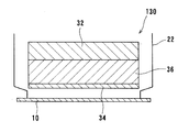
図1に示すように、電極ヘッド30は、内部に収容された板状の陽極電極32と、電極ヘッド30の下面に取り付けられた電流制御部材34とを備えている。また、基板保持部20に保持された基板10の上方には、電極ヘッド30の下部外周部を囲繞する略円筒状のシール材22が配置されている。このシール材22は下方に行くにつれて径が小さくなっている。基板保持部20が基板10を保持した状態で上昇すると、基板10の周縁部がシール材22に当接して、このシール材22と基板10によってシール材22の内方にめっき室24が区画形成される。
As shown in FIG. 1, the
また、このシール材22の外方には、基板10の周縁部に当接する電気接点26が配置されており、基板保持部20が基板10を保持した状態で上昇すると、基板10の周縁部がシール材22の外方で電気接点26に接触して基板10が陰極となるようになっている。
In addition, an
本実施形態における電解処理装置によれば、基板保持部20で基板10を保持して基板保持部20を上昇させ、基板10の上面の周縁部をシール材22に当接させることで、めっき室24を区画形成すると同時に基板10を陰極にする。そして、めっき液をめっき室24の内部に供給し、このめっき室24内のめっき液に陽極電極32と基板10の表面とを浸漬させる。この状態で、電源(図示せず)により陽極電極32と基板10との間に所定の電圧を印加することで、基板10の表面にめっきを施すことができる。
According to the electrolytic processing apparatus in the present embodiment, the
本実施形態においては、図1に示すように、基板保持部20、支持軸42、モータ44により、基板10と陽極電極32および電流制御部材34との間の相対位置を位置決めする位置決め機構が構成されている。この位置決め機構は、電解加工中、基板10と陽極電極32および電流制御部材34との間の相対位置を一定に維持する。
In the present embodiment, as shown in FIG. 1, a positioning mechanism that positions the relative position between the
上述した電流制御部材34について詳細に説明する。図2は、電流制御部材の第1の例を示す概略図である。図2は、電流制御部材としてマスク134を用いた例を示している。このマスク134は、例えばプラスチックのような絶縁物で作られた円板に、電気力線が通過可能なように微細な孔をあけたものである。これらの孔は、基板10の表面に形成された凹凸に対応して配置されている。すなわち、基板10の表面に形成された凹凸に対応して開口比(開口面積比)が設定されている。
The above-described
例えば、電解処理を促進したい幅広な凹部10aの上方に位置する部分134aは孔の開口比を大きく設定し、電解処理を抑制したい幅狭な凹部10bの上方に位置する部分134bは孔の開口比を小さく設定する。マスク134のその他の部分134cは、部分134aの開口比と部分134bの開口比との間の中程度の開口比となるように調整する。孔の開口面積の調整は、孔の大きさ、数、ピッチなどを調整することで調整できる。また、このマスク134と基板10との間のクリアランスは任意に調整可能である。マスク134の孔から基板10までの間における電気力線の過剰な広がりを抑制するため、このクリアランスは、孔の相当径1に対して0〜100の範囲で設定するのが好ましい。
For example, the
図3は、電流制御部材の第2の例を示す概略図である。図3は、電流制御部材として多孔質部材234を用いた例を示している。この多孔質部材234は、基板10の表面に形成された凹凸に対応した気孔率を有しており、気孔率を適切に調整することで電場を制御するものである。多孔質部材234としては、例えばプラスチック製の焼結体やフィルター、セラミックス多孔質部材を用いることができるが、これらに限定されるものではない。
FIG. 3 is a schematic view showing a second example of the current control member. FIG. 3 shows an example in which a
この多孔質部材234の電場制御の原理は、上述したマスク10の原理と同様である。すなわち、電解処理を促進したい凹部10aの上方に位置する部分234aは気孔率を高く設定し、電解処理を抑制したい凹部10bの上方に位置する部分234bは気孔率を小さく設定する。多孔質部材234のその他の部分234cは、部分234aの気孔率と部分234bの気孔率との間の中程度の気孔率となるように調整する。
The principle of the electric field control of the
図4は、電流制御部材の第3の例を示す概略図である。図4は、電流制御部材として凹凸部材334を用いた例を示している。この凹凸部材334は、基板10の表面に形成された凹凸に対応した表面段差を有しており、その厚さを適切に調整することで電場を制御するものである。
FIG. 4 is a schematic view showing a third example of the current control member. FIG. 4 shows an example in which an
この凹凸部材334の電場制御の原理は、凹凸部材334と基板10との間に存在する電解質の量を制御することで、電場を制御するものである。すなわち、基板10と凹凸部材334との間の距離が短い場合(凹凸部材334の厚さが厚い場合)は、通電を担う電解質の濃度(金属イオンや促進剤、抑制剤)が相対的に減少するので、この部分における電解処理の成長を抑制することができる。例えば、電解処理を促進したい幅広な凹部10aの上方に位置する部分334aは基板10との距離を大きく(厚さを薄く)設定し、電解処理を抑制したい幅狭な凹部10bの上方に位置する部分334bは基板10との距離を小さく(厚さを厚く)設定する。凹凸部材334のその他の部分334cは、部分334aの厚さと部分334bの厚さとの間の中程度の厚さとなるように調整する。なお、通常は、凹凸部材30と基板10とを非接触の状態で使用するが、これらを接触させた状態で用いてもよい。
The principle of the electric field control of the
なお、上述したマスク134、多孔質部材234、凹凸部材334などの電流制御部材の加工精度は、基板に形成された凹凸の幅とほぼ同じオーダーであることが好ましい。
The processing accuracy of the current control members such as the
ところで、基板10に形成される凹凸のサイズは、通常、ミクロンからサブミクロンの範囲であり、非常に微細なものである。したがって、基板10と上述した電流制御部材34との間の平面的な位置合わせの精度が高いことが必要となる。また、基板10と電流制御部材34との平面上の相対位置が加工中一定に維持されることが必要である。そのために、レーザーその他の光学的機構を用いた位置決め機構や基板と電流制御部材34とが常に一定の位置関係に維持されるような同軸回転機構などを設けてもよい。このとき、陽極電極32は電流制御部材34とともに移動するのが一般的であると考えられるが、必ずしも陽極電極32を移動する必要はない。
By the way, the size of the unevenness formed on the
図5は、本発明の第2の実施形態における電解処理装置の要部を示す概略図である。図5に示すように、この電解処理装置の電極ヘッド130は、陽極電極32と電流制御部材34との間に配置された高抵抗構造体(電解質含浸体)36を備えている。この高抵抗構造体36は、アルミナ、SiC、ムライト、ジルコニア、チタニア、コージライト等の多孔質セラミックスまたはポリプロピレンやポリエチレンの焼結体等の硬質多孔質体、あるいはこれらの複合体、さらには織布や不織布で構成される。例えば、アルミナ系セラミックスの場合には、ポア径30〜200μmのものが使用され、SiCの場合には、ポア径30μm以下、気孔率20〜95%、厚み1〜20mm、好ましくは5〜20mm、さらに好ましくは8〜15mm程度のものが使用される。例えば、気孔率30%、平均ポア径100μmのアルミナ製多孔質セラミックス板から構成される。
FIG. 5 is a schematic view showing the main part of the electrolytic treatment apparatus in the second embodiment of the present invention. As shown in FIG. 5, the
このような高抵抗構造体36の内部にめっき液を含有させることで、この内部にめっき液を複雑に入り込ませ、厚さ方向にかなり長い経路を辿らせることができる。したがって、多孔質セラミックス板自体は絶縁体であるが、高抵抗構造体36がめっき液の電気伝導率より小さい電気伝導率を有するように構成されている。この高抵抗構造体36によって大きな抵抗を発生させることで、陽極電極32と電流制御部材34との間の電場を均一化することができ、これにより基板10上のめっき膜の面内均一性を向上させることができる。
By containing the plating solution in such a
なお、電流制御部材34としては、上述の第1の実施形態と同様に、基板の凹凸に対応した開口比で孔が形成されたマスク、凹凸に対応した気孔率を有する多孔質部材、あるいは凹凸に対応した表面段差を有する凹凸部材を用いることができる。
As in the first embodiment, the
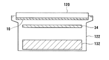
図6は、本発明の第3の実施形態における電解処理装置の要部を示す概略図である。図6に示すように、この電解処理装置は、いわゆるフェイスダウン式のめっき装置であり、基板10をその表面(被めっき面)を下向きにして保持する基板保持部120と、この基板保持部120の下方に板状の陽極電極132と、基板10と陽極電極132を囲繞する略円筒状のめっき槽122とを備えている。基板10と陽極電極132との間には、上述した電流制御部材34が配置されている。
FIG. 6 is a schematic view showing the main part of the electrolytic treatment apparatus in the third embodiment of the present invention. As shown in FIG. 6, this electrolytic processing apparatus is a so-called face-down type plating apparatus, and holds a
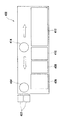
本発明は、図7および図8に示すような電解処理装置400にも適用することができる。この電解処理装置400は、図7に示すように、基板搬送容器402との間で基板を受け渡しする搬送装置404と、基板の基板ホルダ452(図8参照)への着脱を行う基板着脱部406と、基板ホルダ450の保管および一時仮置きを行うストッカ408と、基板の洗浄を行う洗浄ユニット410と、基板に対して電解処理を行う電解処理ユニット412と、基板を装填した基板ホルダ450を基板着脱部406、ストッカ408、洗浄ユニット410、電解処理ユニット412の間で搬送する搬送装置414とを備えている。
The present invention can also be applied to an
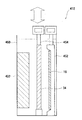
図8に示すように、電解処理ユニット412は、内部にめっき液を保持するめっき槽450と、めっき槽450内に配置された陽極電極432とを備えている。めっき槽450のめっき液には、基板10が装填された基板ホルダ452が浸漬されている。また、この電解処理ユニット412には、上述した電流制御部材34を装填した電流制御部材ホルダ454が浸漬されており、この電流制御部材ホルダ454は陽極電極432と基板10との間に出し入れ自在となっている。
As shown in FIG. 8, the
基板の表面に形成される凹凸構造は基板によって異なるので、基板に対して適切な電流制御部材を選択して使用する必要がある。図8に示す例では、電流制御部材34を装填した電流制御部材ホルダ454が差し替え可能となっているので、処理する基板に応じて適切な電流制御部材34を用いて電解処理を行うことができる。なお、ストッカ408には、電流制御部材ホルダ454に装填された複数の種類の電流制御部材34が保管されている。
Since the uneven structure formed on the surface of the substrate differs depending on the substrate, it is necessary to select and use an appropriate current control member for the substrate. In the example shown in FIG. 8, since the current
従来の方法を用いてLSI配線形成用のめっき工程を行った場合、1μmの膜厚のめっき膜を形成したとき、ディッシング量は1μm、マウンディング量は0.5μmであり、成膜後の表面段差は1.5μm(=1μm+0.5μm)であった。これに対して、本発明の電解処理装置によれば、ディッシング量は0.2μm、マウンディング量は0.1μmに減少し、この結果、成膜後の表面段差を0.3μm(=0.2μm+0.1μm)まで低減することができた。これにより、後段のCMP工程における平坦化性能を大幅に改善することができた。 When the plating process for forming the LSI wiring is performed using the conventional method, when the plating film having a thickness of 1 μm is formed, the dishing amount is 1 μm and the mounting amount is 0.5 μm. The level difference was 1.5 μm (= 1 μm + 0.5 μm). On the other hand, according to the electrolytic processing apparatus of the present invention, the dishing amount is reduced to 0.2 μm and the mounting amount is reduced to 0.1 μm. As a result, the surface level difference after film formation is 0.3 μm (= 0.. 2 μm + 0.1 μm). As a result, the planarization performance in the subsequent CMP process can be greatly improved.
また、従来の方法を用いてチップ実装におけるメタル貫通プラグめっきを行った場合において、直径100μmのビアを埋めるために50μmのめっきを行うと、その結果、めっき表面には30μmの段差が生じた。これに対して、本発明によれば、めっき表面の段差は10μmに低減された。また、めっき膜の膜厚自体も50μmから30μmに減らすことができた。これは、本発明によれば、凹部への選択的な電解処理を行うことができ、凹部以外への電解処理が不要になったためである。 In addition, when metal through plug plating in chip mounting was performed using a conventional method, if 50 μm plating was performed to fill a via having a diameter of 100 μm, a step of 30 μm was generated on the plating surface. In contrast, according to the present invention, the step on the plating surface was reduced to 10 μm. In addition, the thickness of the plating film itself could be reduced from 50 μm to 30 μm. This is because according to the present invention, the selective electrolytic treatment to the concave portion can be performed, and the electrolytic treatment to other than the concave portion becomes unnecessary.
これまで本発明の一実施形態について説明したが、本発明は上述の実施形態に限定されず、その技術的思想の範囲内において種々異なる形態にて実施されてよいことは言うまでもない。 Although one embodiment of the present invention has been described so far, it is needless to say that the present invention is not limited to the above-described embodiment, and may be implemented in various forms within the scope of the technical idea.
10 基板
20,120 基板保持部
22 シール材
24 めっき室
26 電気接点
30,130 電極ヘッド
32,132,432 陽極電極
34,134,234,334 電流制御部材
36 高抵抗構造体
40 アーム
42 支持軸
44 モータ
122,450 めっき槽
400 電解処理装置
402 基板搬送容器
404,414 搬送装置
406 基板着脱部
408 ストッカ
410 洗浄ユニット
412 電解処理ユニット
452 基板ホルダ
454 電流制御部材ホルダ
DESCRIPTION OF
Claims (15)
基板と前記電極との間に電圧を印加する電源と、
基板と前記電極との間に配置され、基板の表面の凹凸に対応して電解処理の促進と抑制を行う電流制御部材と、
を備えたことを特徴とする電解処理装置。 An electrode facing the substrate having irregularities formed on the surface;
A power source for applying a voltage between the substrate and the electrode;
A current control member that is disposed between the substrate and the electrode and that promotes and suppresses the electrolytic treatment corresponding to the irregularities on the surface of the substrate;
An electrolytic treatment apparatus comprising:
基板の表面の凹凸に対応して電解処理の促進と抑制を行う電流制御部材を基板と前記電極との間に配置しつつ、基板と前記電極との間に電圧を印加して電解処理を行うことを特徴とする電解処理方法。 The electrode is made to face the substrate with irregularities formed on the surface,
Electrolytic treatment is performed by applying a voltage between the substrate and the electrode while arranging a current control member between the substrate and the electrode for promoting and suppressing the electrolytic treatment corresponding to the unevenness of the surface of the substrate. An electrolytic treatment method characterized by the above.
Priority Applications (1)
| Application Number | Priority Date | Filing Date | Title |
|---|---|---|---|
| JP2004115834A JP2005298886A (en) | 2004-04-09 | 2004-04-09 | Electrolytic treatment apparatus and method |
Applications Claiming Priority (1)
| Application Number | Priority Date | Filing Date | Title |
|---|---|---|---|
| JP2004115834A JP2005298886A (en) | 2004-04-09 | 2004-04-09 | Electrolytic treatment apparatus and method |
Publications (1)
| Publication Number | Publication Date |
|---|---|
| JP2005298886A true JP2005298886A (en) | 2005-10-27 |
Family
ID=35330798
Family Applications (1)
| Application Number | Title | Priority Date | Filing Date |
|---|---|---|---|
| JP2004115834A Pending JP2005298886A (en) | 2004-04-09 | 2004-04-09 | Electrolytic treatment apparatus and method |
Country Status (1)
| Country | Link |
|---|---|
| JP (1) | JP2005298886A (en) |
Cited By (4)
| Publication number | Priority date | Publication date | Assignee | Title |
|---|---|---|---|---|
| JP2008280555A (en) * | 2007-05-08 | 2008-11-20 | Daisho Denshi:Kk | Plating equipment |
| JP2009218302A (en) * | 2008-03-09 | 2009-09-24 | Fujikura Ltd | Method and device for electrolytic plating of semiconductor substrate |
| JP2010047841A (en) * | 2008-08-25 | 2010-03-04 | Snecma | Device and method for allowing coating film to be deposited on workpiece by electrodeposition |
| JP2017222905A (en) * | 2016-06-15 | 2017-12-21 | 富士通株式会社 | Shielding sheet for electroplating |
-
2004
- 2004-04-09 JP JP2004115834A patent/JP2005298886A/en active Pending
Cited By (4)
| Publication number | Priority date | Publication date | Assignee | Title |
|---|---|---|---|---|
| JP2008280555A (en) * | 2007-05-08 | 2008-11-20 | Daisho Denshi:Kk | Plating equipment |
| JP2009218302A (en) * | 2008-03-09 | 2009-09-24 | Fujikura Ltd | Method and device for electrolytic plating of semiconductor substrate |
| JP2010047841A (en) * | 2008-08-25 | 2010-03-04 | Snecma | Device and method for allowing coating film to be deposited on workpiece by electrodeposition |
| JP2017222905A (en) * | 2016-06-15 | 2017-12-21 | 富士通株式会社 | Shielding sheet for electroplating |
Similar Documents
| Publication | Publication Date | Title |
|---|---|---|
| TW590846B (en) | Planarization of substrates using electrochemical mechanical polishing | |
| TW523558B (en) | Method and apparatus for electrochemical mechanical deposition | |
| TWI555121B (en) | Method and device for filling interconnect structure | |
| US20010024691A1 (en) | Semiconductor substrate processing apparatus and method | |
| CN1701136B (en) | Small force electrochemical mechanical treatment method and equipment | |
| JP2000232078A (en) | Plating method and plating equipment | |
| US20080035474A1 (en) | Apparatus for electroprocessing a substrate with edge profile control | |
| TW201904720A (en) | Chemical mechanical polishing system and method | |
| US20040163950A1 (en) | Planar plating apparatus | |
| US20060091005A1 (en) | Electolytic processing apparatus | |
| US20090061743A1 (en) | Method of soft pad preparation to reduce removal rate ramp-up effect and to stabilize defect rate | |
| JP2005298886A (en) | Electrolytic treatment apparatus and method | |
| KR100465465B1 (en) | Electrolytic plating device and method of the same | |
| KR20020022600A (en) | Plating apparatus and plating method for substrate | |
| US20080277787A1 (en) | Method and pad design for the removal of barrier material by electrochemical mechanical processing | |
| US20090061741A1 (en) | Ecmp polishing sequence to improve planarity and defect performance | |
| US20070181441A1 (en) | Method and apparatus for electropolishing | |
| JP2003306793A (en) | Plating apparatus and plating method | |
| US7025860B2 (en) | Method and apparatus for the electrochemical deposition and removal of a material on a workpiece surface | |
| JP2007051374A (en) | Electroprocessing method and substrate treatment method | |
| JP2007050506A (en) | Apparatus for electrochemical machining | |
| JP2007113082A (en) | Plating device and plating method | |
| CN101435100B (en) | Fluid zone control device and method of operation thereof | |
| KR102499511B1 (en) | Electrolytic treatment jig and electrolytic treatment method | |
| WO2003090965A1 (en) | Polishing method, polishing device, and method of manufacturing semiconductor equipment |