JP2005296964A - Flash welding method and flash welding apparatus - Google Patents
Flash welding method and flash welding apparatus Download PDFInfo
- Publication number
- JP2005296964A JP2005296964A JP2004112850A JP2004112850A JP2005296964A JP 2005296964 A JP2005296964 A JP 2005296964A JP 2004112850 A JP2004112850 A JP 2004112850A JP 2004112850 A JP2004112850 A JP 2004112850A JP 2005296964 A JP2005296964 A JP 2005296964A
- Authority
- JP
- Japan
- Prior art keywords
- voltage
- workpieces
- compensation circuit
- welding
- flash welding
- Prior art date
- Legal status (The legal status is an assumption and is not a legal conclusion. Google has not performed a legal analysis and makes no representation as to the accuracy of the status listed.)
- Withdrawn
Links
Images
Landscapes
- Generation Of Surge Voltage And Current (AREA)
Abstract
【課題】 フラッシュ溶接中に発生するアークを適切に制御し、突合せ端面に形成されるクレータの発生を防止し、端面に一様な溶融層を形成することのできるフラッシュ溶接方法及びフラッシュ溶接装置を提供する。
【解決手段】 溶接電源出力側の2端子を2つの被溶接物1とそれぞれ結合して2つの被溶接物間をフラッシュ溶接するフラッシュ溶接方法において、2つの被溶接物間を補償回路6を介して結合し、被溶接物間に印加する出力電圧と同じ位相を有し無負荷時と同じ電圧波形の電圧を基準電圧VDとし、被溶接物間の電圧V2と基準電圧VDとの差の絶対値(差電圧ΔV)が予め定めた閾値VSを超えたときは、補償回路6を通して電流を流すことによって差電圧ΔVを閾値電圧VS以下とすることを特徴とするフラッシュ溶接方法及びフラッシュ溶接装置。
【選択図】 図1
PROBLEM TO BE SOLVED: To provide a flash welding method and a flash welding apparatus capable of appropriately controlling an arc generated during flash welding, preventing generation of a crater formed on a butt end face, and forming a uniform molten layer on the end face. provide.
In a flash welding method in which two terminals on the output side of a welding power source are coupled to two workpieces 1 and flash welding is performed between the two workpieces, a compensation circuit 6 is provided between the two workpieces. The voltage having the same phase as the output voltage applied between the workpieces and having the same voltage waveform as when there is no load is defined as the reference voltage V D, and the voltage V 2 between the workpieces and the reference voltage V D are When the absolute value of the difference (difference voltage ΔV) exceeds a predetermined threshold value V S , the difference voltage ΔV is set to be equal to or lower than the threshold voltage V S by flowing a current through the compensation circuit 6. And flash welding equipment.
[Selection] Figure 1
Description
本発明は、フラッシュ溶接方法及びフラッシュ溶接装置に関するものである。 The present invention relates to a flash welding method and a flash welding apparatus.
フラッシュ溶接は、2つの被溶接物の突合せ端面を適切な速度で接近させ、局部的な接触部を生じさせることにより、高電流密度の短絡電流により抵抗発熱させ、接触短絡部の溶融破断に伴い発生するアークで局部的集中加熱をさせる。この短絡・アーク、主にアークによって端面の溶融金属が飛散するフラッシングが起こり、このフラッシングによって端面全体の温度を上昇させ(フラッシュ過程)、突合せ端面の全面にほぼ一様な溶融層を形成させた時点で、急速に加圧・変形を加えて溶接部を形成する(アプセット過程)溶接法である。フラッシュ溶接については、例えば非特許文献1に詳しく記載されている。
In flash welding, the butt end surfaces of two workpieces are brought close to each other at an appropriate speed, and a local contact portion is generated, so that resistance heat is generated by a short-circuit current having a high current density. Local concentrated heating is caused by the generated arc. This short-circuiting / arcing, mainly the flashing that the molten metal on the end face is scattered by the arc, raises the temperature of the whole end face by this flushing (flash process), and forms a substantially uniform molten layer on the entire butt end face. At this point, the welding method is to rapidly apply pressure and deformation to form a weld (upset process). The flash welding is described in detail in
フラッシュ溶接において、溶接電源出力側の2端子を2つの被溶接物とそれぞれ結合し、両者間に電圧を印加している。フラッシュ過程においては、被溶接物の突合せ端面の一点において被溶接物同士が接触すると、この接触部には高電流密度の短絡電流が流れる。この短絡電流による抵抗発熱で、接触短絡部は急速に加熱されて溶融にいたり、端面間には溶融ブリッジが形成される。次に、溶融ブリッジはそこを流れる短絡電流がもたらすピンチ力によって破断され、アークが発生する。このアーク点孤時に衝撃的な部分的圧力上昇を生じ、周辺のガスや金属蒸気を急膨張させ、付近の溶融金属は吹き飛ばされることになる。その結果、端面には溶融金属が残存するが、一部は金属粒子となって飛散する。これをフラッシングと呼ぶ。 In flash welding, two terminals on the welding power source output side are respectively coupled to two workpieces and a voltage is applied between them. In the flash process, when the workpieces come into contact with each other at one point on the butt end surface of the workpiece, a short-circuit current with a high current density flows through the contact portion. Due to the resistance heat generated by this short-circuit current, the contact short-circuited portion is rapidly heated and melts, or a melting bridge is formed between the end faces. The melt bridge is then broken by the pinch force provided by the short-circuit current flowing therethrough and an arc is generated. When this arc point is isolated, a shocking partial pressure rise is caused, the surrounding gas and metal vapor are rapidly expanded, and the nearby molten metal is blown away. As a result, the molten metal remains on the end face, but part of the molten metal is scattered as metal particles. This is called flushing.
フラッシュ過程において、突合せ端面に一様な溶融層を形成する上で、アーク発熱は主要な働きをしている。一方で、アークはそのアーク力により端面溶融金属を吹き飛ばすので、熱損失をもたらし、かつ溶融金属を過剰に吹き飛ばして端面にクレータを形成することとなる。端面にクレータが形成されると、いわゆるペネトレータと呼ばれる内部欠陥が生じやすいといわれいてる。フラッシュ過程においては、端面は比較的なめらかでかつ端面全面にほぼ均一に溶融層が見られる状態に近づけることが重要で、このようにするには、アークを適切に制御する必要がある。 In the flash process, arc heat generation plays a major role in forming a uniform molten layer on the butt end face. On the other hand, since the arc blows off the end face molten metal by the arc force, it causes heat loss and excessively blows off the molten metal to form a crater on the end face. It is said that when a crater is formed on the end face, an internal defect called a so-called penetrator is likely to occur. In the flash process, it is important that the end face be relatively smooth and close to a state where a molten layer can be seen almost uniformly over the entire end face. To do this, the arc must be controlled appropriately.
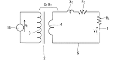
フラッシュ過程において被溶接物端面接触部の短絡が破れてアークが発生するとき、アークの大きさは、溶接電源出力側と被溶接物との間に形成される二次側の無負荷電圧および電源回路の誘導リアクタンスの影響を受ける。誘導リアクタンスが大きいほど、アーク発生によって形成されるクレータは深くなり、継ぎ手破面で観察される欠陥(フラットスポットなど)の占める面積が増大する傾向にある。 When an arc is generated by breaking the short circuit at the contact portion of the work piece end face during the flash process, the size of the arc is determined by the no-load voltage and power supply on the secondary side formed between the welding power source output side and the work piece. It is affected by the inductive reactance of the circuit. The larger the inductive reactance, the deeper the crater formed by the arc generation, and the area occupied by defects (such as flat spots) observed on the joint fracture surface tends to increase.
溶接電源として交流電源を用いる場合、図2に示すように、電源回路の誘導リアクタンスは、電源変圧器の誘導リアクタンスXT、および二次側導体の幾何学的配置によって定まる誘導リアクタンスXCに分けられるが、一般にフラッシュ溶接装置では、電源変圧器の誘導リアクタンスは大きい値であり、これを直接小さな値に改変することは困難である。そのため、二次側導体の幾何学的配置を工夫し、幾何学的配置によって定まる二次導体の誘導リアクタンスXCを低減することによってアークの適切化が図られているが限度があり、アークの適切化は十分には図られていない。 When an AC power source is used as the welding power source, as shown in FIG. 2, the inductive reactance of the power circuit is divided into an inductive reactance X T of the power transformer and an inductive reactance X C determined by the geometrical arrangement of the secondary conductor. However, in general, in the flash welding apparatus, the inductive reactance of the power transformer is a large value, and it is difficult to directly change it to a small value. Therefore, the geometry of the secondary conductor is devised, and the induction of the arc is reduced by reducing the inductive reactance X C of the secondary conductor determined by the geometry, but there is a limit. Adequacy is not fully planned.
本発明は、フラッシュ溶接中に発生するアークを適切に制御し、突合せ端面に形成されるクレータの発生を防止し、端面に一様な溶融層を形成することのできるフラッシュ溶接方法及びフラッシュ溶接装置を提供することを目的とする。 The present invention relates to a flash welding method and a flash welding apparatus capable of appropriately controlling an arc generated during flash welding, preventing generation of a crater formed on a butt end face, and forming a uniform molten layer on the end face. The purpose is to provide.
即ち、本発明の要旨とするところは以下の通りである。
(1)溶接電源出力側の2端子を2つの被溶接物1とそれぞれ結合して2つの被溶接物間をフラッシュ溶接するフラッシュ溶接方法において、2つの被溶接物間を補償回路6を介して結合し、被溶接物間に印加する出力電圧と同じ位相を有し無負荷時と同じ電圧波形の電圧を基準電圧VDとし、被溶接物間の電圧V2と基準電圧VDとの差の絶対値(以下「差電圧ΔV」という。)が予め定めた閾値VSを超えたときは、補償回路6を通して電流を流すことによって差電圧ΔVを閾値電圧VS以下とすることを特徴とするフラッシュ溶接方法。
(2)補償回路6は、差電圧ΔVが閾値VSを超えたときに導通するスイッチング素子を有することを特徴とする請求項1に記載のフラッシュ溶接方法。
(3)溶接電源出力側の2端子を2つの被溶接物とそれぞれ結合して2つの被溶接物間をフラッシュ溶接するフラッシュ溶接方法において、出力側の各端子16付近とその端子と結合した被溶接物1の溶接側端部付近との間を、補償回路6を介して結合し、補償回路6のスイッチング素子7は、スイッチング素子両端の電圧が予め定めた閾値を超えたときに導通することを特徴とするフラッシュ溶接方法。
That is, the gist of the present invention is as follows.
(1) In a flash welding method in which two terminals on the welding power source output side are coupled to two
(2) The flash welding method according to
(3) In a flash welding method in which two terminals on the welding power source output side are coupled to two workpieces and flash welding is performed between the two workpieces, the vicinity of each
(4)溶接電源出力側の2端子を2つの被溶接物とそれぞれ結合して2つの被溶接物間をフラッシュ溶接するフラッシュ溶接装置において、2つの被溶接物間を結合する補償回路6を有し、被溶接物間に印加する出力電圧と同じ位相を有し無負荷時と同じ電圧波形の電圧を基準電圧VDとし、補償回路6は、被溶接物間の電圧V2と基準電圧VDとの差の絶対値(差電圧ΔV)が予め定めた閾値VSを超えたときに電流を流し、これによって差電圧を閾値電圧以下とすることを特徴とするフラッシュ溶接装置。
(5)補償回路6は、差電圧ΔVが閾値VSを超えたときに導通するスイッチング素子7を有することを特徴とする請求項4に記載のフラッシュ溶接装置。
(6)溶接電源出力側の2端子を2つの被溶接物とそれぞれ結合して2つの被溶接物間をフラッシュ溶接するフラッシュ溶接装置において、前記出力側の各端子16とその端子と結合した被溶接物1の溶接側端部付近との間を介して結合する補償回路6を有し、補償回路6のスイッチング素子7は、スイッチング素子両端の電圧が予め定めた閾値を超えたときに導通することを特徴とするフラッシュ溶接装置。
(4) In a flash welding apparatus that couples two terminals on the welding power source output side with two workpieces and flash welds between the two workpieces, a
(5) The flash welding apparatus according to
(6) In a flash welding apparatus in which two terminals on the welding power source output side are respectively coupled to two workpieces and flash welding is performed between the two workpieces, each
本発明のフラッシュ溶接方法及びフラッシュ溶接装置は、溶接電源出力側の2端子を2つの被溶接物とそれぞれ結合して形成される溶接回路に補償回路を挿入し、アーク発生時に余剰の電流をこの補償回路を経由して流すことによりアークを適切に制御し、突合せ端面に形成されるクレータの発生を防止し、端面に一様な溶融層を形成することを可能にする。 In the flash welding method and the flash welding apparatus of the present invention, a compensation circuit is inserted into a welding circuit formed by joining two terminals on the welding power source output side with two workpieces, and an excess current is generated when an arc is generated. By flowing through the compensation circuit, the arc is appropriately controlled, the generation of craters formed on the butt end faces is prevented, and a uniform molten layer can be formed on the end faces.
フラッシュ溶接電源としては交流電源と直流電源とがあり、本発明は交流・直流のいずれの場合にも適用することができる。以下、交流電源を用いた場合を例にとって説明を行う。 As the flash welding power source, there are an AC power source and a DC power source, and the present invention can be applied to both cases of AC and DC. Hereinafter, the case where an AC power supply is used will be described as an example.
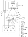
フラッシュ溶接装置は、図1に示すように被溶接物1を突合せ状態に設定する固定台11と移動台12、および移動台12を前進させ、かつ被溶接物1に加圧力を加える移動台送り装置13、電力を供給する溶接変圧器2と通電制御装置9から構成される。
As shown in FIG. 1, the flash welding apparatus advances the
溶接変圧器2の一次コイル3には440V程度の交流電圧が印加され、この結果として溶接変圧器の二次側(二次コイル4)に二次電圧として8V程度の交流電圧が生成される。被溶接物1を固定台11と移動台12にそれぞれ固着するためのクランプ10が電極を兼ね、2個の被溶接物1をそれぞれ固定台11と移動台12に固着した後、被溶接物1に溶接変圧器2の二次電圧が印加される。
An AC voltage of about 440V is applied to the
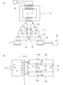
本発明の第1の実施の形態においては、図1に示すように、2つの被溶接物(1a、1b)間を補償回路6を介して結合する。そして被溶接物間に印加する出力電圧と同じ位相を有し無負荷時と同じ電圧波形の電圧を基準電圧VDとし、被溶接物間の電圧V2と基準電圧VDとの差の絶対値(差電圧ΔV)が予め定めた閾値VSを超えたときは、補償回路6を通して電流を流す。
In the first embodiment of the present invention, two workpieces (1a, 1b) are coupled via a
ここで、上記基準電圧VDとは、無負荷時における二次電圧に等しい電圧である。一方、被溶接物間の短絡電流が破断されたときには、被溶接物間に誘導起電力が発生し、この誘導起電力に基づいてアークが点孤される。誘導起電力が発生したとき、被溶接物間の電圧は基準電圧と誘導起電力とが足し合わされた電圧となる。即ち、上記差電圧ΔVが、誘導起電力を意味することとなる。そこで、上記のように差電圧ΔVが予め定めた閾値VSを超えたときに補償回路6を通して電流を流すようにしてやれば、誘導起電力に起因する電流の一部が補償回路6を通じて流れ、残りの電流が被溶接物間を流れてアークを形成することとなる。そして、これによって差電圧を閾値電圧以下とすれば、アークの強度を閾値電圧で規定される強度以下とすることができ、アークを適切に制御してクレータの生成を防止することができるのである。
Here, the reference voltage V D is a voltage equal to the secondary voltage at the time of no load. On the other hand, when the short-circuit current between the workpieces is broken, an induced electromotive force is generated between the workpieces, and the arc is ignited based on the induced electromotive force. When the induced electromotive force is generated, the voltage between the workpieces is a voltage obtained by adding the reference voltage and the induced electromotive force. That is, the difference voltage ΔV means an induced electromotive force. Therefore, if a current is caused to flow through the
基準電圧VDは、溶接変圧器2に一次電圧を供給している一次電源15において電圧検出手段17aによって(無負荷の)一次電圧V1を検出し、この一次電圧V1に溶接変圧器2の二次電圧と一次電圧との比をかけることによって生成することができる。
Reference voltage V D, the
次に被溶接物間の電圧V2を検出し、基準電圧VDとの差の絶対値(差電圧ΔV)を算出する。差電圧ΔVが予め定めた閾値VSを超えたときに、補償回路6に対して指令を発し、補償回路6を通じて被溶接物間に電流を流す。補償回路6における電流のオン・オフは、スイッチング素子7によることとすると好ましい。このとき補償回路6は、差電圧が閾値を超えたときに導通するスイッチング素子7を有することとなる。被溶接物間に流れる電流は、補償回路6においてスイッチング素子7と直列に接続する抵抗素子8の抵抗値によって調整することができる。抵抗素子8の抵抗値が低いほど、アーク発生時に補償回路6を流れる電流が多くなり、アークの強度が弱くなる。
Next, the voltage V 2 between the workpieces is detected, and the absolute value (difference voltage ΔV) of the difference from the reference voltage V D is calculated. When the difference voltage ΔV exceeds a predetermined threshold value V S , a command is issued to the
補償回路内にスイッチング素子7と抵抗素子8との直列回路を2組並列に配置することができる。被溶接物間の電圧と基準電圧との差がプラスで閾値を超えたときに第1のスイッチング素子7aを導通し、被溶接物間の電圧と基準電圧との差がマイナスでその絶対値が閾値を超えたときに第2のスイッチング素子7bを導通するようにすれば、結果として差電圧が閾値を超えたときに補償回路を通して電流を流すことが可能となる。
Two sets of series circuits of the
基準電圧VDの生成、被溶接物間の電圧V2と基準電圧VDとの対比および差電圧ΔVの算出、補償回路6のスイッチング素子7への指令などは、フラッシュ溶接装置の通電制御装置9内において行うことができる。
Generation of the reference voltage V D, the calculation of the contrast and the difference voltage ΔV between the voltage V 2 and the reference voltage V D between the object to be welded, etc. command to the
本発明の第2の実施の形態においては、図3(a)に示すように、溶接電源出力側の2端子を2つの被溶接物とそれぞれ結合して2つの被溶接物間をフラッシュ溶接するフラッシュ溶接方法において、出力側の各端子16とその端子と結合した被溶接物1の溶接側端部付近との間を、補償回路6を介して結合し、補償回路6のスイッチング素子7は、スイッチング素子両端の電圧が予め定めた閾値を超えたときに導通することを特徴とする。
In the second embodiment of the present invention, as shown in FIG. 3A, the two terminals on the welding power source output side are respectively coupled to the two workpieces and flash welding is performed between the two workpieces. In the flash welding method, each terminal 16 on the output side and the vicinity of the welding side end of the
前述のとおり、溶接電源として交流電源を用いる場合、電源回路の誘導リアクタンスは、溶接変圧器の誘導リアクタンスXT、および二次側導体の幾何学的配置によって定まる二次導体の誘導リアクタンスXCに分けられる。これら誘導リアクタンスの総合的な効果としてアークの強度および持続時間が定まる。ここにおいて、二次側導体の幾何学的配置によって定まる二次導体の誘導リアクタンスXCに起因する誘導起電力分のみを低減することによっても、アークを弱めることが可能である。 As described above, when an AC power source is used as the welding power source, the inductive reactance of the power supply circuit is equal to the inductive reactance X T of the welding transformer and the inductive reactance X C of the secondary conductor determined by the geometric arrangement of the secondary side conductor. Divided. The overall effect of these inductive reactances is to determine the arc intensity and duration. Here, it is also possible to weaken the arc by reducing only the induced electromotive force due to the inductive reactance X C of the secondary conductor determined by the geometric arrangement of the secondary side conductor.
上記本発明の第2の実施の形態においては、図3(b)に示すように、溶接電源出力側の端子16aと被溶接物1aとの間の二次側導体5が有する誘導リアクタンスXCaに起因する誘導起電力を補償回路6aで検出し、この起電力が予め定めた閾値を超えたときに導通するので、二次側導体5aが有する誘導リアクタンスに起因する誘導起電力に基づく電流が補償回路内に流れ、結果として被溶接物間のアークを弱めることが可能となる。溶接電源出力側の端子16bと被溶接物1bとの間の二次側導体5bが有する誘導リアクタンスXCbに起因する誘導起電力に基づく電流も同様に補償回路6bに流れ、結果として被溶接物間のアークを弱めることが可能となる。
In the second embodiment of the present invention, as shown in FIG. 3 (b), the inductive reactance X C included in the
第2の実施の形態において、補償回路6のスイッチング素子7としてバリスタを用いることとすると好ましい。バリスタは電圧によって抵抗値が非直線的に変化する抵抗体であり、その特性を適正に選択することにより、バリスタ両端の電圧が上記閾値を超えたときに電流を流す制御を行わせることができる。バリスタの特性が対称性を有するときには各被溶接物毎の補償回路内に1個のバリスタを用いたスイッチング素子を有することとすればよい。バリスタの特性が非対称性である場合には、補償回路内に2個のバリスタを並列に配置することによって対称性を実現することができる。
In the second embodiment, it is preferable to use a varistor as the switching
本発明は、電圧波形が正弦波状の通常の交流電源を用いる場合の他、電源波形が矩形波その他の正弦波以外の波形であっても用いることができる。また、溶接電源として直流電源を用いる場合であっても適用することが可能である。 The present invention can be used not only when a normal AC power supply having a sine wave voltage waveform is used, but also when the power supply waveform is a rectangular wave or other waveform other than a sine wave. Further, the present invention can be applied even when a DC power source is used as a welding power source.
溶接変圧器の一次電圧が440V、二次電圧が13Vの溶接変圧器を用いるフラッシュ溶接装置において、本発明を適用した。フラッシュ溶接装置は、被溶接物を突合せ状態に設定する固定台と移動台、および移動台を前進させ、かつ被溶接物に加圧力を加える移動台送り装置、電力を供給する溶接変圧器と通電制御装置から構成される。溶接変圧器の二次側端子とクランプとが結線されており、被溶接物をクランプで固着することによって2つの二次側端子と2個の被溶接物とがそれぞれ結線される。 The present invention was applied to a flash welding apparatus using a welding transformer having a primary voltage of 440V and a secondary voltage of 13V. The flash welding equipment consists of a fixed base and a moving base for setting the workpieces in a butt state, a moving base feeding device for moving the moving base forward and applying pressure to the workpiece, a welding transformer for supplying electric power, and energization It consists of a control device. The secondary terminal of the welding transformer and the clamp are connected to each other, and the two secondary terminals and the two objects to be welded are respectively connected by fixing the object to be welded with the clamps.
(実施例1)
図1に示すように、2つの被溶接物1間を補償回路6を介して結合する本発明を実施した。
(Example 1)
As shown in FIG. 1, the present invention in which two
補償回路6は、スイッチング素子7と抵抗素子8との直列回路を2組並列に配置している。スイッチング素子7としてはIGBT素子を用いた。抵抗素子8の抵抗値は、溶接後の被溶接部の曲げ試験結果が最良になる様に定める。補償回路6の両端を2つの被溶接物1にそれぞれ接続する。接続場所は被溶接物が溶接時に軟化する範囲の外側でできるだけ両端の接続点の距離が小さい所とした。
In the
スイッチング素子7のオンオフは、通電制御装置9からの指令によってなされる。通電制御装置においては、まず基準電圧VDを生成する。基準電圧VDは、溶接変圧器2に一次電圧を供給している電源と同じ一次電源15において無負荷状態における一次電圧V1を電圧検出手段17aによって検出し、この一次電圧V1に溶接変圧器の二次電圧と一次電圧との比をかけることによって生成する。一次電圧波形を溶接変圧器の巻き数比αを割ることによって基準電圧を定めることもできる。被溶接物間の電圧V2を、被溶接物に接続した補償回路の両端電圧として電圧検出手段17bによって検出する。次に、被溶接物間の電圧V2と基準電圧VDとの差を検出し、差の値がプラスで閾値VSを超えたときに第1のスイッチング素子7aを導通し、被溶接物間の電圧と基準電圧との差がマイナスでその絶対値が閾値を超えたときに第2のスイッチング素子7bを導通するように、通電制御装置9からスイッチング素子7にオン・オフ指令20を発する。これにより、差電圧ΔV(被溶接物間の電圧と基準電圧との差の絶対値)が閾値VSを超えたときに補償回路6を通して電流を流すことができる。なお、閾値電圧VSを3Vとした。
The switching
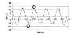
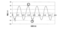
これにより、差電圧が閾値電圧を超えるアーク発生時に、電流の一部を補償回路側に流すことにより、差電圧を閾値電圧以下とすることができる。結果を図4に示す。図4は、横軸が時間、縦軸が被溶接物間の電圧を示す。アークが生成された2ヶ所(図中○印)の時間において、被溶接物間のピーク電圧が基準電圧+3V以下に収まっていることがわかる。 Thereby, when an arc in which the difference voltage exceeds the threshold voltage is generated, a part of the current is allowed to flow to the compensation circuit side, so that the difference voltage can be made equal to or less than the threshold voltage. The results are shown in FIG. In FIG. 4, the horizontal axis represents time, and the vertical axis represents the voltage between the workpieces. It can be seen that the peak voltage between the workpieces is within the reference voltage +3 V or less at the time of the two places (circles in the figure) where the arc was generated.
この結果、溶接中のフラッシュ過程において突合せ端面にクレータが形成されず、端面に一様な溶融層を形成することができた。 As a result, a crater was not formed on the butt end face during the flash process during welding, and a uniform molten layer could be formed on the end face.
(実施例2)
図3(a)に示すように、出力側の各端子とその端子と結合した被溶接物の溶接側端部付近との間を、補償回路6を介して結合する本発明を実施した。
(Example 2)
As shown in FIG. 3A, the present invention was implemented in which each terminal on the output side and the vicinity of the weld side end of the work piece coupled to the terminal are coupled via a
補償回路6はスイッチング素子7と抵抗素子8との直列回路とし、スイッチング素子7としてバリスタを使用した。バリスタの導通電圧が1.5Vのものを使用した。補償回路6は、溶接変圧器2の二次側端子16と被溶接物1との間に接続し、2個の二次側端子と2個の被溶接物の双方にそれぞれ補償回路6を接続した。非溶接部側における接続場所は、被溶接物が溶接時に軟化する範囲の外側でできるだけ両端の接続点の距離が小さい所とした。
The
これにより、アーク発生時において、溶接変圧器の二次側端子16と被溶接物1との間の二次導体5の部分で発生する1.5V以上の誘導起電力については、その誘導起電力に起因する電流は補償回路6を流れることとなり、非溶接物間で発生するアークを弱めることができた。結果を図5に示す。図5は、横軸が時間、縦軸が被溶接物間の電圧を示す。アークが生成された2ヶ所(図中○印)の時間において、被溶接物間のピーク電圧が基準電圧+3V以下に収まっていることがわかる。
Thus, when an arc is generated, an induced electromotive force of 1.5 V or more generated in the portion of the
この結果、溶接中のフラッシュ過程において突合せ端面にクレータが形成されず、端面に一様な溶融層を形成することができた。 As a result, a crater was not formed on the butt end face during the flash process during welding, and a uniform molten layer could be formed on the end face.
1 被溶接物
2 溶接変圧器
3 一次コイル
4 二次コイル
5 二次導体
6 補償回路
7 スイッチング素子
8 抵抗素子
9 通電制御装置
10 クランプ
11 固定台
12 移動台
13 移動台送り装置
15 一次電源
16 端子
17 電圧検出手段
20 オン・オフ指令
VD 基準電圧
V1 一次電圧
V2 被溶接物間電圧
ΔV 差電圧
VS 閾値電圧
XT 溶接変圧器の誘導リアクタンス
RT 溶接変圧器の純抵抗
XC 二次導体の誘導リアクタンス
RC 二次導体の純抵抗
RL 被溶接物の純抵抗
DESCRIPTION OF
Claims (6)
Priority Applications (1)
| Application Number | Priority Date | Filing Date | Title |
|---|---|---|---|
| JP2004112850A JP2005296964A (en) | 2004-04-07 | 2004-04-07 | Flash welding method and flash welding apparatus |
Applications Claiming Priority (1)
| Application Number | Priority Date | Filing Date | Title |
|---|---|---|---|
| JP2004112850A JP2005296964A (en) | 2004-04-07 | 2004-04-07 | Flash welding method and flash welding apparatus |
Publications (1)
| Publication Number | Publication Date |
|---|---|
| JP2005296964A true JP2005296964A (en) | 2005-10-27 |
Family
ID=35329146
Family Applications (1)
| Application Number | Title | Priority Date | Filing Date |
|---|---|---|---|
| JP2004112850A Withdrawn JP2005296964A (en) | 2004-04-07 | 2004-04-07 | Flash welding method and flash welding apparatus |
Country Status (1)
| Country | Link |
|---|---|
| JP (1) | JP2005296964A (en) |
Cited By (1)
| Publication number | Priority date | Publication date | Assignee | Title |
|---|---|---|---|---|
| JP2011011253A (en) * | 2009-07-06 | 2011-01-20 | Sumitomo Metal Ind Ltd | Method for monitoring welding quality in upsetting butt welding, monitoring device therefor, and method for producing welded product by upsetting butt welding |
-
2004
- 2004-04-07 JP JP2004112850A patent/JP2005296964A/en not_active Withdrawn
Cited By (1)
| Publication number | Priority date | Publication date | Assignee | Title |
|---|---|---|---|---|
| JP2011011253A (en) * | 2009-07-06 | 2011-01-20 | Sumitomo Metal Ind Ltd | Method for monitoring welding quality in upsetting butt welding, monitoring device therefor, and method for producing welded product by upsetting butt welding |
Similar Documents
| Publication | Publication Date | Title |
|---|---|---|
| US8253056B2 (en) | Resistance welding method and resistance welding apparatus | |
| JP5234042B2 (en) | Arc welding method and apparatus | |
| US10071436B2 (en) | Methods and systems for resistance spot welding using direct current micro pulses | |
| CN107073624A (en) | Reverse pulse welding system and method | |
| US8664568B2 (en) | Arc welding control method and arc welding apparatus | |
| CN104096948B (en) | For the method and apparatus by controlling welding current to carry out electric arc welding | |
| JPWO1997043073A1 (en) | Horizontal welding method and welding equipment | |
| JP2019136748A (en) | Resistance spot welding method | |
| US9221116B2 (en) | Inductive discharge arc re-ignition and stabilizing circuit | |
| KR102149744B1 (en) | Composite welder | |
| JP6754935B2 (en) | Arc welding control method | |
| JP2005296964A (en) | Flash welding method and flash welding apparatus | |
| JP6417640B2 (en) | Hot wire welding system | |
| CN109648174B (en) | Arc striking method of automatic welding system | |
| EP1068041A1 (en) | Method for arc welding with melting electrode | |
| KR101221052B1 (en) | Resistance spot welding method | |
| JP2022045136A (en) | Welding power source system | |
| JP2002205172A (en) | Resistance welding method and apparatus | |
| JP2017035707A (en) | One-side spot welding method and welding apparatus | |
| EP4691678A1 (en) | Arc-start processes for long stick out submerged arc welding | |
| KR200236717Y1 (en) | Portable welding apparatus have a electrode holder | |
| KR101850804B1 (en) | Power supply for shielded metal arc welding of waveform control type with built in welding database | |
| JP6712967B2 (en) | Welding machine | |
| JPH09267183A (en) | Control device of flash butt welding machine | |
| CN111745270A (en) | Method and apparatus for converting welding power into welding power and resistance preheating power |
Legal Events
| Date | Code | Title | Description |
|---|---|---|---|
| A300 | Withdrawal of application because of no request for examination |
Free format text: JAPANESE INTERMEDIATE CODE: A300 Effective date: 20070703 |