JP2005295503A - High-frequency module and high-frequency circuit for mobile communication device - Google Patents

High-frequency module and high-frequency circuit for mobile communication device Download PDF

Info

Publication number
JP2005295503A
JP2005295503A JP2005008577A JP2005008577A JP2005295503A JP 2005295503 A JP2005295503 A JP 2005295503A JP 2005008577 A JP2005008577 A JP 2005008577A JP 2005008577 A JP2005008577 A JP 2005008577A JP 2005295503 A JP2005295503 A JP 2005295503A
Authority
JP
Japan
Prior art keywords
transmission signal
terminal
coupler
frequency module
frequency
Prior art date
Legal status (The legal status is an assumption and is not a legal conclusion. Google has not performed a legal analysis and makes no representation as to the accuracy of the status listed.)
Withdrawn
Application number
JP2005008577A
Other languages
Japanese (ja)
Inventor
Masashi Suga
誠志 須賀
Gerard Cunningham
ジェラード・カニンガム
Current Assignee (The listed assignees may be inaccurate. Google has not performed a legal analysis and makes no representation or warranty as to the accuracy of the list.)
TDK Corp
Original Assignee
TDK Corp
Priority date (The priority date is an assumption and is not a legal conclusion. Google has not performed a legal analysis and makes no representation as to the accuracy of the date listed.)
Filing date
Publication date
Application filed by TDK Corp filed Critical TDK Corp
Publication of JP2005295503A publication Critical patent/JP2005295503A/en
Withdrawn legal-status Critical Current

Links

Images

Classifications

    • HELECTRICITY
    • H04ELECTRIC COMMUNICATION TECHNIQUE
    • H04BTRANSMISSION
    • H04B1/00Details of transmission systems, not covered by a single one of groups H04B3/00 - H04B13/00; Details of transmission systems not characterised by the medium used for transmission
    • H04B1/38Transceivers, i.e. devices in which transmitter and receiver form a structural unit and in which at least one part is used for functions of transmitting and receiving
    • H04B1/40Circuits
    • H04B1/44Transmit/receive switching
    • H04B1/48Transmit/receive switching in circuits for connecting transmitter and receiver to a common transmission path, e.g. by energy of transmitter
    • HELECTRICITY
    • H04ELECTRIC COMMUNICATION TECHNIQUE
    • H04BTRANSMISSION
    • H04B1/00Details of transmission systems, not covered by a single one of groups H04B3/00 - H04B13/00; Details of transmission systems not characterised by the medium used for transmission
    • H04B1/02Transmitters
    • H04B1/04Circuits
    • H04B2001/0408Circuits with power amplifiers
    • H04B2001/0416Circuits with power amplifiers having gain or transmission power control

Landscapes

  • Engineering & Computer Science (AREA)
  • Computer Networks & Wireless Communication (AREA)
  • Signal Processing (AREA)
  • Transceivers (AREA)
  • Transmitters (AREA)

Abstract

<P>PROBLEM TO BE SOLVED: To secure sufficient isolation in a directional coupler while a high-frequency switch and the directional coupler can be unified. <P>SOLUTION: A high-frequency module 11 includes a high-frequency switch 21 and a coupler 22. Either of a transmission signal terminal 11b and a receive signal terminal 11c is selectively connected to an antenna terminal 11a through the high-frequency switch 21. The coupler 22 provided between the transmission terminal 11b and the high-frequency switch 21 detects a transmission signal. The coupler 22 has a main line S1 and a sub-line S2 which are put in electromagnetic coupling. The sub-line S2 has a width narrower than that of the main line S1. In this case, X is within a range from 10 to 21 and Y is 21 or larger, where -XdB is the coupling degree C of the coupler 22, and -YdB is the directivity D of the coupler 22. <P>COPYRIGHT: (C)2006,JPO&NCIPI

Description

本発明は、通信機器における送信信号および受信信号を処理するための高周波モジュールおよび、この高周波モジュールを含む移動体通信機器用高周波回路に関する。   The present invention relates to a high-frequency module for processing a transmission signal and a reception signal in a communication device and a high-frequency circuit for mobile communication device including the high-frequency module.

近年、携帯電話機、自動車電話機等の移動体通信機器は、飛躍的に普及してきている。移動体通信機器には、1つのアンテナを送信と受信とに共用させるために送信信号の経路と受信信号の経路とを切り替える高周波モジュールを備えているものがある。この高周波モジュールは、例えば、送受信の経路を切り替える高周波スイッチを備えている。また、この高周波モジュールは、例えば、複数の構成要素が多層基板によって一体化されて、表面実装部品(SMD)化される。このような高周波スイッチを備えた高周波モジュールは、例えば、特許文献1に記載されている。   In recent years, mobile communication devices such as mobile phones and automobile phones have been rapidly spreading. Some mobile communication devices include a high-frequency module that switches between a transmission signal path and a reception signal path in order to share one antenna for transmission and reception. The high-frequency module includes, for example, a high-frequency switch that switches between transmission and reception paths. In addition, in the high-frequency module, for example, a plurality of components are integrated by a multilayer substrate to form a surface mount component (SMD). A high-frequency module including such a high-frequency switch is described in Patent Document 1, for example.

上記高周波スイッチは、アンテナに接続されるアンテナポート、送信信号が入力される送信信号ポート、および受信信号を出力する受信信号ポートを有している。移動体通信機器においては、一般的に、高周波スイッチの送信信号ポートには、レベルがほぼ一定になるように調整された送信信号が入力されるようになっている。送信信号のレベルの調整は、ゲインを制御可能な電力増幅器と、送信信号を検出する方向性結合器(以下、カプラとも言う。)と、自動出力制御回路(以下、APC回路とも言う。)を用いて、以下のようにして行なわれる。すなわち、送信回路から出力された送信信号は、電力増幅器によって増幅された後、カプラを経て、高周波スイッチの送信信号ポートに供給される。カプラは、電力増幅器より出力された送信信号を検出し、この送信信号に対応したモニタ信号をAPC回路に出力する。APC回路は、モニタ信号のレベルに応じて、すなわち送信信号のレベルに応じて、電力増幅器の出力信号のレベルがほぼ一定になるように、電力増幅器のゲインを制御する。   The high-frequency switch has an antenna port connected to an antenna, a transmission signal port to which a transmission signal is input, and a reception signal port for outputting a reception signal. In a mobile communication device, generally, a transmission signal adjusted so as to have a substantially constant level is input to a transmission signal port of a high frequency switch. The level of the transmission signal is adjusted by using a power amplifier capable of controlling the gain, a directional coupler (hereinafter also referred to as a coupler) for detecting the transmission signal, and an automatic output control circuit (hereinafter also referred to as an APC circuit). And is performed as follows. That is, the transmission signal output from the transmission circuit is amplified by the power amplifier and then supplied to the transmission signal port of the high-frequency switch via the coupler. The coupler detects the transmission signal output from the power amplifier and outputs a monitor signal corresponding to the transmission signal to the APC circuit. The APC circuit controls the gain of the power amplifier so that the level of the output signal of the power amplifier becomes substantially constant according to the level of the monitor signal, that is, according to the level of the transmission signal.

携帯電話機等の移動体通信機器では、小型化および軽量化が求められている。そのため、移動体通信機器では、その構成部品についても、小型化、一体化および部品点数の削減が求められている。このような事情から、例えば特許文献2ないし5に示されるように、多層基板を用いて、高周波スイッチとカプラを一体化することが提案されている。   Mobile communication devices such as cellular phones are required to be smaller and lighter. Therefore, mobile communication devices are required to be downsized, integrated, and reduced in the number of components for the components. Under such circumstances, for example, as disclosed in Patent Documents 2 to 5, it has been proposed to integrate a high-frequency switch and a coupler using a multilayer substrate.

特開平9−36603号公報JP 9-36603 A 特開2002−43813号公報JP 2002-43813 A 特開2002−300080号公報Japanese Patent Laid-Open No. 2002-300080 特開2002−300081号公報Japanese Patent Laid-Open No. 2002-300081 特開2002−300082号公報JP 2002-300082 A

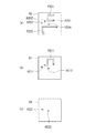
ここで、図20を参照して、高周波スイッチとカプラを一体化する場合の問題点について説明する。図20は、移動体通信機器における高周波回路の構成の一例を示すブロック図である。図20に示した高周波回路は、アンテナ101に接続される高周波スイッチ111と、送信信号端子102と、受信信号端子103とを備えている。送信信号端子102は、図示しない送信回路に接続され、この送信回路からの送信信号が入力される。受信信号端子103は、図示しない受信回路に接続され、この受信回路に対して受信信号を出力する。   Here, with reference to FIG. 20, a problem when the high-frequency switch and the coupler are integrated will be described. FIG. 20 is a block diagram showing an example of the configuration of a high-frequency circuit in a mobile communication device. The high-frequency circuit shown in FIG. 20 includes a high-frequency switch 111 connected to the antenna 101, a transmission signal terminal 102, and a reception signal terminal 103. The transmission signal terminal 102 is connected to a transmission circuit (not shown) and receives a transmission signal from the transmission circuit. The reception signal terminal 103 is connected to a reception circuit (not shown) and outputs a reception signal to the reception circuit.

高周波スイッチ111は、アンテナ101に接続されるアンテナポート111aと、このアンテナポート111aに選択的に接続される送信信号ポート111bおよび受信信号ポート111cを有している。   The high frequency switch 111 has an antenna port 111a connected to the antenna 101, and a transmission signal port 111b and a reception signal port 111c that are selectively connected to the antenna port 111a.

高周波回路は、更に、電力増幅器112、カプラ113、APC回路114、終端抵抗115およびアイソレータ116を備えている。電力増幅器112は、入力端と出力端とゲイン制御端とを有している。電力増幅器112の入力端は、送信信号端子102に接続されている。   The high frequency circuit further includes a power amplifier 112, a coupler 113, an APC circuit 114, a termination resistor 115, and an isolator 116. The power amplifier 112 has an input end, an output end, and a gain control end. The input terminal of the power amplifier 112 is connected to the transmission signal terminal 102.

カプラ113は、入力ポートP01、出力ポートP02、モニタポートP03およびアイソレートポートP04を有している。また、カプラ113は、電磁結合する一対のストリップラインである主ラインS01および副ラインS02を有している。そして、主ラインS01の一端が入力ポートP01、他端が出力ポートP02になっている。また、副ラインS02の一端がモニタポートP03、他端がアイソレートポートP04になっている。入力ポートP01は、電力増幅器112の出力端に接続されている。出力ポートP02は、アイソレータ116の入力端に接続されている。モニタポートP03は、APC回路114の入力端に接続されている。アイソレートポートP04は、終端抵抗115を介して接地されている。   The coupler 113 has an input port P01, an output port P02, a monitor port P03, and an isolated port P04. The coupler 113 has a main line S01 and a sub line S02 which are a pair of strip lines that are electromagnetically coupled. One end of the main line S01 is an input port P01, and the other end is an output port P02. One end of the sub-line S02 is a monitor port P03, and the other end is an isolated port P04. The input port P01 is connected to the output terminal of the power amplifier 112. The output port P02 is connected to the input terminal of the isolator 116. The monitor port P03 is connected to the input terminal of the APC circuit 114. The isolated port P04 is grounded via the termination resistor 115.

APC回路114の出力端は、電力増幅器112のゲイン制御端に接続されている。APC回路114は、カプラ113のモニタポートP03から出力されるモニタ信号のレベルに応じて、すなわち送信信号のレベルに応じて、電力増幅器112の出力信号のレベルがほぼ一定になるように、電力増幅器112のゲインを制御する。   The output end of the APC circuit 114 is connected to the gain control end of the power amplifier 112. The APC circuit 114 is a power amplifier that adjusts the level of the output signal of the power amplifier 112 according to the level of the monitor signal output from the monitor port P03 of the coupler 113, that is, according to the level of the transmission signal. The gain of 112 is controlled.

アイソレータ116の出力端は、高周波スイッチ111のポート111bに接続されている。アイソレータ116は、入力端から出力端へ進む信号は通過させ、出力端から入力端へ進む信号は阻止する。   The output terminal of the isolator 116 is connected to the port 111 b of the high frequency switch 111. The isolator 116 passes a signal traveling from the input end to the output end, and blocks a signal traveling from the output end to the input end.

高周波回路は、更に、フィルタ117とローノイズアンプ118とを備えている。フィルタ117の入力端は、高周波スイッチ111のポート111cに接続されている。フィルタ117の出力端は、ローノイズアンプ118の入力端に接続されている。フィルタ117は、受信信号のうちの不要な信号成分を抑制する。ローノイズアンプ118の出力端は、受信信号端子103に接続されている。   The high frequency circuit further includes a filter 117 and a low noise amplifier 118. The input end of the filter 117 is connected to the port 111 c of the high frequency switch 111. The output end of the filter 117 is connected to the input end of the low noise amplifier 118. The filter 117 suppresses unnecessary signal components in the received signal. The output terminal of the low noise amplifier 118 is connected to the reception signal terminal 103.

図20に示した高周波回路では、送信時には、高周波スイッチ111のポート111a,111bが接続される。このとき、送信信号端子102に入力された送信信号は、電力増幅器112、カプラ113、アイソレータ116および高周波スイッチ111を経て、アンテナ101から発信される。一方、受信時には、高周波スイッチ111のポート111a,111cが接続される。このとき、アンテナ101に入力された受信信号は、高周波スイッチ111、フィルタ117およびローノイズアンプ118を経て、受信信号端子103より受信回路に出力される。   In the high frequency circuit shown in FIG. 20, the ports 111a and 111b of the high frequency switch 111 are connected during transmission. At this time, the transmission signal input to the transmission signal terminal 102 is transmitted from the antenna 101 via the power amplifier 112, the coupler 113, the isolator 116, and the high frequency switch 111. On the other hand, at the time of reception, the ports 111a and 111c of the high frequency switch 111 are connected. At this time, the reception signal input to the antenna 101 is output from the reception signal terminal 103 to the reception circuit via the high frequency switch 111, the filter 117, and the low noise amplifier 118.

図20に示した高周波回路では、アンテナ101とカプラ113のモニタポートP03との間のアイソレーションを十分に大きくする必要がある。このアイソレーションの大きさが十分ではない場合には、送信信号の一部がアンテナ101で反射されて生じる反射信号がモニタポートP03に到達し、その結果、モニタポートP03より出力されるモニタ信号にノイズが重畳されることになる。すると、電力増幅器112の出力レベルを正確に制御することができなくなる。   In the high-frequency circuit shown in FIG. 20, it is necessary to sufficiently increase the isolation between the antenna 101 and the monitor port P03 of the coupler 113. If the isolation is not sufficient, a reflected signal generated by reflecting a part of the transmission signal by the antenna 101 reaches the monitor port P03, and as a result, the monitor signal output from the monitor port P03 Noise will be superimposed. As a result, the output level of the power amplifier 112 cannot be accurately controlled.

図20に示した高周波回路では、カプラ113と高周波スイッチ111の間にアイソレータ116が挿入されている。そのため、この高周波回路では、アンテナ101とカプラ113のモニタポートP03との間のアイソレーションは、アイソレータ116のアイソレーション(例えば−20dB)とカプラ113のアイソレーション(例えば−30dB)とによって、十分な値となる。   In the high frequency circuit shown in FIG. 20, an isolator 116 is inserted between the coupler 113 and the high frequency switch 111. Therefore, in this high-frequency circuit, the isolation between the antenna 101 and the monitor port P03 of the coupler 113 is sufficient due to the isolation of the isolator 116 (for example, −20 dB) and the isolation of the coupler 113 (for example, −30 dB). Value.

ここで、多層基板を用いて、図20における高周波スイッチ111とカプラ113を一体化する場合について考える。この場合には、高周波スイッチ111とカプラ113の間にアイソレータ116を挿入することはできない。従って、この場合には、アンテナ101とカプラ113のモニタポートP03との間のアイソレーションは、ほぼカプラ113のアイソレーションのみとなる。そのため、この場合には、アンテナ101とカプラ113のモニタポートP03との間のアイソレーションを十分に大きくすることが難しく、電力増幅器112の出力レベルを正確に制御することができなくなるおそれがある。   Here, consider a case where the high frequency switch 111 and the coupler 113 in FIG. 20 are integrated using a multilayer substrate. In this case, the isolator 116 cannot be inserted between the high frequency switch 111 and the coupler 113. Therefore, in this case, the isolation between the antenna 101 and the monitor port P03 of the coupler 113 is almost only the isolation of the coupler 113. Therefore, in this case, it is difficult to sufficiently increase the isolation between the antenna 101 and the monitor port P03 of the coupler 113, and the output level of the power amplifier 112 may not be accurately controlled.

なお、特許文献2には、誘電体層を挟んで重ね合わされた主線路と副線路とを有するカプラにおいて、副線路の幅を主線路の幅よりも狭くして、副線路の線路幅の全域を確実に主線路に対面させることにより、送信出力を高精度に検出できるようにした技術が記載されている。しかしながら、特許文献2では、カプラのアイソレーションを大きくすることについては考慮されていない。   In Patent Document 2, in a coupler having a main line and a sub line that are overlapped with each other with a dielectric layer interposed therebetween, the width of the sub line is made narrower than the width of the main line, and the entire line width of the sub line is set. A technique is described in which the transmission output can be detected with high accuracy by reliably facing the main line. However, Patent Document 2 does not consider increasing the isolation of the coupler.

本発明はかかる問題点に鑑みてなされたもので、その目的は、送信信号および受信信号を処理するための高周波モジュールであって、高周波スイッチと方向性結合器を一体化でき、且つ方向性結合器において十分なアイソレーションを確保できるようにした高周波モジュール、およびこの高周波モジュールを含む移動体通信機器用高周波回路を提供することにある。   The present invention has been made in view of such a problem, and an object thereof is a high-frequency module for processing a transmission signal and a reception signal, in which a high-frequency switch and a directional coupler can be integrated, and directional coupling is achieved. It is an object of the present invention to provide a high-frequency module capable of ensuring sufficient isolation in a device, and a high-frequency circuit for mobile communication equipment including the high-frequency module.

本発明の高周波モジュールは、
アンテナに接続されるアンテナ端子と、
送信信号が入力される送信信号端子と、
受信信号を出力する受信信号端子と、
アンテナ端子に対して送信信号端子と受信信号端子のいずれかを選択的に接続する高周波スイッチと、
送信信号端子と高周波スイッチの間に設けられ、送信信号を検出する方向性結合器と、
交互に積層された誘電体層と導体層とを含む積層体とを備え、
積層体によって高周波モジュールの構成要素が一体化されているものである。
The high frequency module of the present invention is
An antenna terminal connected to the antenna;
A transmission signal terminal to which a transmission signal is input; and
A reception signal terminal for outputting a reception signal;
A high-frequency switch that selectively connects either the transmission signal terminal or the reception signal terminal to the antenna terminal;
A directional coupler that is provided between the transmission signal terminal and the high-frequency switch and detects a transmission signal;
A laminate including alternately laminated dielectric layers and conductor layers;
The components of the high-frequency module are integrated by the laminate.

本発明の高周波モジュールにおいて、方向性結合器は、誘電体層を挟んで対向する主ラインと副ラインとを有し、主ラインは、送信信号端子と高周波スイッチとの間の信号経路に挿入され、副ラインは、主ラインよりも狭い幅を有している。高周波モジュールは、更に、副ラインの一端に接続された終端抵抗を備えている。方向性結合器の結合度を−XdB、方向性結合器の方向性を−YdBとしたとき、Xは10〜21の範囲内であり、Yは21以上である。   In the high-frequency module of the present invention, the directional coupler has a main line and a sub-line that face each other with the dielectric layer interposed therebetween, and the main line is inserted into a signal path between the transmission signal terminal and the high-frequency switch. The sub-line has a narrower width than the main line. The high frequency module further includes a termination resistor connected to one end of the sub line. When the coupling degree of the directional coupler is −X dB and the directionality of the directional coupler is −Y dB, X is in the range of 10 to 21 and Y is 21 or more.

本発明の高周波モジュールでは、方向性結合器の結合度を−XdB、方向性結合器の方向性を−YdBとしたとき、Xを10〜21の範囲内とし、Yを21以上とすることにより、送信信号を検出するという方向性結合器の機能を損なうことなく、方向性結合器のアイソレーションを十分大きくすることができる。   In the high frequency module of the present invention, when the coupling degree of the directional coupler is -X dB and the directionality of the directional coupler is -Y dB, X is in the range of 10 to 21, and Y is 21 or more. The isolation of the directional coupler can be sufficiently increased without impairing the function of the directional coupler for detecting the transmission signal.

本発明の高周波モジュールにおいて、Yは23以上であってもよい。また、副ラインの特性インピーダンスは、主ラインの特性インピーダンスよりも大きくてもよい。また、終端抵抗は積層体に搭載されていてもよい。   In the high frequency module of the present invention, Y may be 23 or more. Further, the characteristic impedance of the sub line may be larger than the characteristic impedance of the main line. Further, the termination resistor may be mounted on the laminate.

また、本発明の高周波モジュールにおいて、高周波スイッチは能動素子と受動素子とを含み、能動素子は積層体に搭載され、受動素子の少なくとも一部は、導体層を用いて構成されていてもよい。この場合、能動素子はダイオードであってもよい。また、導体層を用いて構成された受動素子は、集中定数素子であってもよい。   In the high frequency module of the present invention, the high frequency switch may include an active element and a passive element, the active element may be mounted on the multilayer body, and at least a part of the passive element may be configured using a conductor layer. In this case, the active element may be a diode. In addition, the passive element configured using the conductor layer may be a lumped constant element.

また、本発明の高周波モジュールは、更に、高周波スイッチを動作させるための制御信号が入力される制御端子と、制御端子と高周波スイッチとの間に設けられた電流制限用抵抗とを備え、電流制限用抵抗は積層体に搭載されていてもよい。   The high-frequency module of the present invention further includes a control terminal to which a control signal for operating the high-frequency switch is input, and a current limiting resistor provided between the control terminal and the high-frequency switch. The resistance for use may be mounted on the laminate.

また、本発明の高周波モジュールは、更に、積層体の外面に設けられ、外部回路に接続される接続端子を備えていてもよい。   The high frequency module of the present invention may further include a connection terminal provided on the outer surface of the laminate and connected to an external circuit.

また、本発明の高周波モジュールは、更に、送信信号端子と高周波スイッチの間に設けられ、送信信号のうちの不要な信号成分を抑制するフィルタを備えていてもよい。   The high-frequency module of the present invention may further include a filter that is provided between the transmission signal terminal and the high-frequency switch and suppresses unnecessary signal components in the transmission signal.

また、本発明の高周波モジュールは、更に、送信信号端子と方向性結合器との間に設けられ、送信信号を増幅する電力増幅器を備えていてもよい。   The high-frequency module of the present invention may further include a power amplifier that is provided between the transmission signal terminal and the directional coupler and amplifies the transmission signal.

本発明の移動体通信機器用高周波回路は、本発明の高周波モジュールと、方向性結合器に入力される前の送信信号を増幅する電力増幅器と、方向性結合器によって検出された送信信号のレベルに応じて、電力増幅器のゲインを制御する自動出力制御回路とを含んでいる。   The high-frequency circuit for mobile communication equipment of the present invention includes a high-frequency module of the present invention, a power amplifier that amplifies a transmission signal before being input to the directional coupler, and a level of the transmission signal detected by the directional coupler. And an automatic output control circuit for controlling the gain of the power amplifier.

本発明によれば、高周波スイッチと方向性結合器を一体化でき、且つ、方向性結合器の結合度を−XdB、方向性結合器の方向性を−YdBとしたとき、Xを10〜21の範囲内とし、Yを21以上とすることにより、方向性結合器において十分なアイソレーションを確保することができるという効果を奏する。   According to the present invention, when the high-frequency switch and the directional coupler can be integrated, the coupling degree of the directional coupler is −X dB, and the directionality of the directional coupler is −Y dB, X is 10 to 21. When Y is set to 21 or more, there is an effect that sufficient isolation can be secured in the directional coupler.

以下、本発明の実施の形態について図面を参照して詳細に説明する。
[第1の実施の形態]
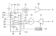
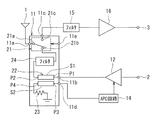
始めに、図1を参照して、本発明の第1の実施の形態に係る高周波モジュールおよび移動体通信機器用高周波回路の構成について説明する。図1は、本実施の形態に係る移動体通信機器用高周波回路の構成を示すブロック図である。本実施の形態に係る高周波モジュールおよび移動体通信機器用高周波回路(以下、単に高周波回路と記す。)は、携帯電話機等の移動体通信機器における送信信号および受信信号を処理するものである。
Hereinafter, embodiments of the present invention will be described in detail with reference to the drawings.
[First Embodiment]
First, with reference to FIG. 1, the configuration of a high-frequency module and a high-frequency circuit for mobile communication devices according to a first embodiment of the present invention will be described. FIG. 1 is a block diagram showing a configuration of a high-frequency circuit for mobile communication equipment according to the present embodiment. A high-frequency module and a mobile communication device high-frequency circuit (hereinafter simply referred to as a high-frequency circuit) according to the present embodiment process transmission signals and reception signals in mobile communication devices such as mobile phones.

図1に示したように、本実施の形態に係る高周波回路は、送信信号端子2と、受信信号端子3と、本実施の形態に係る高周波モジュール11とを備えている。送信信号端子2は、図示しない送信回路に接続され、この送信回路からの送信信号が入力される。受信信号端子3は、図示しない受信回路に接続され、この受信回路に対して受信信号を出力する。高周波モジュール11は、アンテナ1に接続され、このアンテナ1に対して、送信信号端子2と受信信号端子3のいずれかを選択的に接続する。   As shown in FIG. 1, the high frequency circuit according to the present embodiment includes a transmission signal terminal 2, a reception signal terminal 3, and a high frequency module 11 according to the present embodiment. The transmission signal terminal 2 is connected to a transmission circuit (not shown) and receives a transmission signal from the transmission circuit. The reception signal terminal 3 is connected to a reception circuit (not shown) and outputs a reception signal to the reception circuit. The high-frequency module 11 is connected to the antenna 1 and selectively connects either the transmission signal terminal 2 or the reception signal terminal 3 to the antenna 1.

高周波回路は、更に、電力増幅器12、アイソレータ13、自動出力制御回路(以下、APC回路と記す。)14、フィルタ15およびローノイズアンプ16を備えている。電力増幅器12は、入力端と出力端とゲイン制御端とを有している。電力増幅器12の入力端は、送信信号端子2に接続されている。電力増幅器12の出力端は、アイソレータ13の入力端に接続されている。アイソレータ13の出力端は、高周波モジュール11に接続されている。APC回路14の入力端は、高周波モジュール11に接続されている。APC回路14の出力端は、電力増幅器12のゲイン制御端に接続されている。フィルタ15の入力端は、高周波モジュール11に接続されている。フィルタ15の出力端は、ローノイズアンプ16の入力端に接続されている。ローノイズアンプ16の出力端は、受信信号端子3に接続されている。   The high frequency circuit further includes a power amplifier 12, an isolator 13, an automatic output control circuit (hereinafter referred to as an APC circuit) 14, a filter 15, and a low noise amplifier 16. The power amplifier 12 has an input end, an output end, and a gain control end. The input terminal of the power amplifier 12 is connected to the transmission signal terminal 2. The output terminal of the power amplifier 12 is connected to the input terminal of the isolator 13. The output end of the isolator 13 is connected to the high frequency module 11. The input end of the APC circuit 14 is connected to the high frequency module 11. The output end of the APC circuit 14 is connected to the gain control end of the power amplifier 12. The input end of the filter 15 is connected to the high frequency module 11. The output end of the filter 15 is connected to the input end of the low noise amplifier 16. The output terminal of the low noise amplifier 16 is connected to the reception signal terminal 3.

高周波モジュール11は、アンテナ1に接続されるアンテナ端子11aと、送信信号が入力される送信信号端子11bと、受信信号を出力する受信信号端子11cと、モニタ信号を出力するモニタ端子11dと、制御信号が入力される制御端子11eとを備えている。アイソレータ13の出力端は、送信信号端子11bに接続されている。フィルタ15の入力端は、受信信号端子11cに接続されている。APC回路14の入力端は、モニタ端子11dに接続されている。   The high-frequency module 11 includes an antenna terminal 11a connected to the antenna 1, a transmission signal terminal 11b to which a transmission signal is input, a reception signal terminal 11c that outputs a reception signal, a monitor terminal 11d that outputs a monitor signal, and a control And a control terminal 11e to which a signal is input. The output terminal of the isolator 13 is connected to the transmission signal terminal 11b. The input end of the filter 15 is connected to the reception signal terminal 11c. The input end of the APC circuit 14 is connected to the monitor terminal 11d.

高周波モジュール11は、更に、高周波スイッチ21と、方向性結合器(以下、カプラと言う。)22と、終端抵抗23とを備えている。高周波スイッチ21は、アンテナ端子11aに対して送信信号端子11bと受信信号端子11cのいずれかを選択的に接続するものである。カプラ22は、送信信号端子11bと高周波スイッチ21の間に設けられ、送信信号を検出するものである。   The high frequency module 11 further includes a high frequency switch 21, a directional coupler (hereinafter referred to as a coupler) 22, and a termination resistor 23. The high frequency switch 21 selectively connects either the transmission signal terminal 11b or the reception signal terminal 11c to the antenna terminal 11a. The coupler 22 is provided between the transmission signal terminal 11b and the high frequency switch 21 and detects a transmission signal.

高周波スイッチ21は、アンテナ端子11aに接続されるアンテナポート21aと、このアンテナポート21aに選択的に接続される送信信号ポート21bおよび受信信号ポート21cを有している。カプラ22は、送信信号ポート21bと送信信号端子11bとの間に設けられている。受信信号ポート21cは、受信信号端子11cに接続されている。また、制御端子11eは、高周波スイッチ21に接続されている。   The high frequency switch 21 has an antenna port 21a connected to the antenna terminal 11a, and a transmission signal port 21b and a reception signal port 21c that are selectively connected to the antenna port 21a. The coupler 22 is provided between the transmission signal port 21b and the transmission signal terminal 11b. The reception signal port 21c is connected to the reception signal terminal 11c. Further, the control terminal 11 e is connected to the high frequency switch 21.

カプラ22は、入力ポートP1、出力ポートP2、モニタポートP3およびアイソレートポートP4を有している。また、カプラ22は、電磁結合する一対のストリップラインである主ラインS1および副ラインS2を有している。そして、主ラインS1の一端が入力ポートP1、他端が出力ポートP2になっている。また、副ラインS2の一端がモニタポートP3、他端がアイソレートポートP4になっている。入力ポートP1は、送信信号端子11bに接続されている。出力ポートP2は、高周波スイッチ21の送信信号ポート21bに接続されている。モニタポートP3は、モニタ端子11dに接続されている。アイソレートポートP4は、終端抵抗23を介して接地されている。   The coupler 22 has an input port P1, an output port P2, a monitor port P3, and an isolated port P4. The coupler 22 has a main line S1 and a sub line S2 which are a pair of strip lines that are electromagnetically coupled. One end of the main line S1 is an input port P1, and the other end is an output port P2. Further, one end of the sub line S2 is a monitor port P3, and the other end is an isolated port P4. The input port P1 is connected to the transmission signal terminal 11b. The output port P2 is connected to the transmission signal port 21b of the high frequency switch 21. The monitor port P3 is connected to the monitor terminal 11d. The isolated port P4 is grounded via the termination resistor 23.

高周波モジュール11は、更に、交互に積層された誘電体層と導体層とを含む積層体としての多層基板を備えている。そして、この多層基板によって高周波モジュール11の構成要素が一体化されている。多層基板の構成については、後で詳しく説明する。   The high-frequency module 11 further includes a multilayer substrate as a laminate including dielectric layers and conductor layers that are alternately laminated. And the component of the high frequency module 11 is integrated by this multilayer substrate. The configuration of the multilayer substrate will be described in detail later.

APC回路14は、カプラ22のモニタポートP3から出力されるモニタ信号のレベルに応じて、すなわち送信信号のレベルに応じて、電力増幅器12の出力信号のレベルがほぼ一定になるように、電力増幅器12のゲインを制御する。   The APC circuit 14 is a power amplifier so that the level of the output signal of the power amplifier 12 becomes substantially constant according to the level of the monitor signal output from the monitor port P3 of the coupler 22, that is, according to the level of the transmission signal. 12 gain is controlled.

アイソレータ13は、入力端から出力端へ進む信号は通過させ、出力端から入力端へ進む信号は阻止する。アイソレータ13は、送信信号における高調波成分を減衰させる機能も有している。   The isolator 13 passes a signal traveling from the input end to the output end, and blocks a signal traveling from the output end to the input end. The isolator 13 also has a function of attenuating harmonic components in the transmission signal.

フィルタ15は、受信信号のうちの不要な信号成分を抑制する。ローノイズアンプ16は、フィルタ15より出力された受信信号を増幅して、受信信号端子3に出力する。   The filter 15 suppresses unnecessary signal components in the received signal. The low noise amplifier 16 amplifies the reception signal output from the filter 15 and outputs it to the reception signal terminal 3.

フィルタ15は、低域通過フィルタ(以下、LPFと記す。)、帯域通過フィルタ(以下、BPFと記す。)、高域通過フィルタ(以下、HPFと記す。)、帯域阻止フィルタ(以下、BRFと記す。)のいずれであってもよい。また、フィルタ15は、例えば、弾性波素子を用いて構成されていてもよい。弾性波素子は、弾性表面波素子でもよいし、バルク弾性波素子でもよい。   The filter 15 includes a low-pass filter (hereinafter referred to as LPF), a band-pass filter (hereinafter referred to as BPF), a high-pass filter (hereinafter referred to as HPF), a band rejection filter (hereinafter referred to as BRF). Any of the above may be used. Moreover, the filter 15 may be comprised using the elastic wave element, for example. The acoustic wave element may be a surface acoustic wave element or a bulk acoustic wave element.

本実施の形態に係る高周波回路では、制御端子11eに入力される制御信号に応じて、高周波スイッチ21の状態が切り替えられる。送信時には、高周波スイッチ21のポート21a,21bが接続される。このとき、送信信号端子2に入力された送信信号は、電力増幅器12、アイソレータ13、カプラ22および高周波スイッチ21を経て、アンテナ1から発信される。一方、受信時には、高周波スイッチ21のポート21a,21cが接続される。このとき、アンテナ1に入力された受信信号は、高周波スイッチ21、フィルタ15およびローノイズアンプ16を経て、受信信号端子3より受信回路に出力される。カプラ22は、送信信号を検出し、この送信信号に対応したモニタ信号をAPC回路14に出力する。APC回路14は、モニタ信号のレベルに応じて、すなわち送信信号のレベルに応じて、電力増幅器12の出力信号のレベルがほぼ一定になるように、電力増幅器12のゲインを制御する。   In the high-frequency circuit according to the present embodiment, the state of the high-frequency switch 21 is switched according to the control signal input to the control terminal 11e. At the time of transmission, the ports 21a and 21b of the high frequency switch 21 are connected. At this time, the transmission signal input to the transmission signal terminal 2 is transmitted from the antenna 1 through the power amplifier 12, the isolator 13, the coupler 22, and the high frequency switch 21. On the other hand, the ports 21a and 21c of the high frequency switch 21 are connected during reception. At this time, the reception signal input to the antenna 1 is output from the reception signal terminal 3 to the reception circuit via the high-frequency switch 21, the filter 15, and the low noise amplifier 16. The coupler 22 detects the transmission signal and outputs a monitor signal corresponding to the transmission signal to the APC circuit 14. The APC circuit 14 controls the gain of the power amplifier 12 so that the level of the output signal of the power amplifier 12 becomes substantially constant according to the level of the monitor signal, that is, according to the level of the transmission signal.

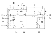
図2は、高周波モジュール11の回路構成の一例を示す回路図である。この例では、高周波モジュール11内の高周波スイッチ21は、一端がアンテナ端子11aに接続されたてキャパシタ31と、一端がキャパシタ31の他端に接続され、他端が接地されたキャパシタ32と、アノードがキャパシタ31の他端に接続され、カソードがカプラ22の出力ポートP2に接続されたダイオード33とを有している。キャパシタ31の一端は、アンテナポート21aに対応する。ダイオード33のカソードは、送信信号ポート21bに対応する。   FIG. 2 is a circuit diagram illustrating an example of a circuit configuration of the high-frequency module 11. In this example, the high frequency switch 21 in the high frequency module 11 includes a capacitor 31 having one end connected to the antenna terminal 11a, a capacitor 32 having one end connected to the other end of the capacitor 31 and the other end grounded, and an anode. Is connected to the other end of the capacitor 31, and the cathode is connected to the output port P 2 of the coupler 22. One end of the capacitor 31 corresponds to the antenna port 21a. The cathode of the diode 33 corresponds to the transmission signal port 21b.

高周波スイッチ21は、更に、一端がキャパシタ31の他端に接続されたコイル34と、一端がコイル34の他端に接続され、他端が受信信号端子11cに接続されたキャパシタ35と、カソードがコイル34の他端に接続されたダイオード36と、一端がダイオード36のアノードに接続され、他端が接地されたキャパシタ37と、一端がダイオード36のアノードに接続され、他端が制御端子11eに接続された電流制限用抵抗38とを有している。キャパシタ35の他端は、受信信号ポート21cに対応する。ダイオード33,36としては、例えばPINダイオードが用いられる。   The high-frequency switch 21 further includes a coil 34 having one end connected to the other end of the capacitor 31, a capacitor 35 having one end connected to the other end of the coil 34, and the other end connected to the reception signal terminal 11c, and a cathode. The diode 36 connected to the other end of the coil 34, one end connected to the anode of the diode 36, the other end grounded, the one end connected to the anode of the diode 36, and the other end to the control terminal 11e. And a current limiting resistor 38 connected thereto. The other end of the capacitor 35 corresponds to the reception signal port 21c. As the diodes 33 and 36, for example, PIN diodes are used.

図2に示した高周波スイッチ21は、能動素子であるダイオード33,36と、受動素子であるキャパシタ31,32,35,37、コイル34および抵抗38とを含んでいる。このうち、ダイオード33,36は多層基板に搭載される。受動素子の少なくとも一部は、多層基板の導体層を用いて構成されていてもよい。多層基板の導体層を用いて構成された受動素子は、集中定数素子であってもよい。多層基板の導体層を用いて構成されない受動素子は、多層基板に搭載される。また、カプラ22の主ラインS1および副ラインS2は、多層基板の導体層を用いて構成される。多層基板に搭載される受動素子は、例えば、キャパシタ31および抵抗23,38である。   The high-frequency switch 21 shown in FIG. 2 includes diodes 33 and 36 that are active elements, capacitors 31, 32, 35, and 37 that are passive elements, a coil 34, and a resistor 38. Among these, the diodes 33 and 36 are mounted on a multilayer substrate. At least a part of the passive element may be configured using a conductor layer of a multilayer substrate. The passive element configured using the conductor layer of the multilayer substrate may be a lumped constant element. Passive elements that are not configured using the conductor layers of the multilayer substrate are mounted on the multilayer substrate. Further, the main line S1 and the subline S2 of the coupler 22 are configured using a conductor layer of a multilayer substrate. Passive elements mounted on the multilayer substrate are, for example, a capacitor 31 and resistors 23 and 38.

図2に示した高周波モジュール11では、送信時には、制御端子11eに印加される制御信号がハイレベルとなる。その結果、2つのダイオード33,36が共に導通状態となる。このとき、コイル34、キャパシタ32,37およびダイオード36のインダクタンス成分による共振によって、コイル34を経由する信号経路のインピーダンスが大きくなり、アンテナ端子11aと受信信号端子11cとの間の信号経路は遮断される。そのため、送信信号端子11bに入力された送信信号は、ダイオード33およびキャパシタ31を通過してアンテナ端子11aに送られ、アンテナ1から送信される。このときダイオード33,36に要求される特性は、信号を通すために、オン抵抗が小さいことである。   In the high-frequency module 11 shown in FIG. 2, the control signal applied to the control terminal 11e becomes high level during transmission. As a result, the two diodes 33 and 36 are both conductive. At this time, due to resonance due to the inductance components of the coil 34, capacitors 32 and 37, and the diode 36, the impedance of the signal path passing through the coil 34 increases, and the signal path between the antenna terminal 11a and the reception signal terminal 11c is cut off. The Therefore, the transmission signal input to the transmission signal terminal 11 b passes through the diode 33 and the capacitor 31 and is sent to the antenna terminal 11 a and transmitted from the antenna 1. At this time, the characteristic required for the diodes 33 and 36 is that the on-resistance is small in order to pass signals.

一方、受信時には、制御端子11eに印加される制御信号がローレベルとなる。その結果、2つのダイオード33,36が共に非導通状態となる。これにより、ダイオード33,36を経由する信号経路は遮断される。そのため、アンテナ1に入力された受信信号は、キャパシタ31、コイル34、キャパシタ35を通過して、受信信号端子11cより出力される。このときダイオード33,36に要求される特性は、信号を通過させないために、キャパシタンスが小さいことである。   On the other hand, at the time of reception, the control signal applied to the control terminal 11e becomes low level. As a result, the two diodes 33 and 36 are both turned off. As a result, the signal path passing through the diodes 33 and 36 is blocked. Therefore, the reception signal input to the antenna 1 passes through the capacitor 31, the coil 34, and the capacitor 35 and is output from the reception signal terminal 11c. At this time, the characteristic required for the diodes 33 and 36 is that the capacitance is small so as not to pass a signal.

図2に示した例では、高周波スイッチ21において、能動素子としてダイオードを用いているが、このダイオードの代わりに、例えば、GaAs化合物半導体による電界効果トランジスタを用いてもよい。   In the example shown in FIG. 2, a diode is used as an active element in the high-frequency switch 21, but a field effect transistor made of, for example, a GaAs compound semiconductor may be used instead of this diode.

また、図2に示した高周波モジュール11において、電流制限用抵抗38は、省略してもよい。   In the high-frequency module 11 shown in FIG. 2, the current limiting resistor 38 may be omitted.

本実施の形態において、カプラ22の主ラインS1と副ラインS2は、多層基板の誘電体層を挟んで対向している。主ラインS1は、送信信号端子11bと高周波スイッチ21との間の信号経路に挿入されている。副ラインS2は、主ラインS1よりも狭い幅を有している。   In the present embodiment, the main line S1 and the subline S2 of the coupler 22 are opposed to each other with the dielectric layer of the multilayer substrate interposed therebetween. The main line S1 is inserted in a signal path between the transmission signal terminal 11b and the high frequency switch 21. The sub line S2 has a narrower width than the main line S1.

次に、本実施の形態におけるカプラ22の特性について説明する。まず、カプラ22の結合度、アイソレーションおよび方向性について説明する。ここでは、カプラ22のポートP1〜P4に入力される信号またはポートP1〜P4より出力される信号のレベルも、P1〜P4で表す。また、結合度、アイソレーションおよび方向性を、それぞれC(dB)、I(dB)、D(dB)で表す。これらは、以下の式で表される。   Next, the characteristics of the coupler 22 in the present embodiment will be described. First, the coupling degree, isolation, and directionality of the coupler 22 will be described. Here, the levels of signals input to the ports P1 to P4 of the coupler 22 or signals output from the ports P1 to P4 are also represented by P1 to P4. In addition, the degree of coupling, isolation, and directionality are represented by C (dB), I (dB), and D (dB), respectively. These are represented by the following equations.

C=10log(P3/P1)、
I=10log(P4/P1)=10log(P3/P2)、
D=10log(P4/P3)
C = 10 log (P3 / P1),
I = 10 log (P4 / P1) = 10 log (P3 / P2),
D = 10 log (P4 / P3)

また、方向性Dの式は、以下のように変形でき、これにより、方向性DはI−Cで表される。   In addition, the equation for the directionality D can be modified as follows, whereby the directionality D is represented by I-C.

D=10log(P4/P3)
=10log(P4/P1)−10log(P3/P1)
=10log(P3/P2)−10log(P3/P1)
=I−C
D = 10 log (P4 / P3)
= 10 log (P4 / P1) -10 log (P3 / P1)
= 10 log (P3 / P2) -10 log (P3 / P1)
= I-C

本実施の形態では、カプラ22のポートP4は、終端抵抗23によって終端されている。そのため、ポートP4の信号レベルを測定することができない。そこで、本実施の形態では、方向性Dは、上記の式のように、[アイソレーションI−結合度C]より求める。   In the present embodiment, the port P4 of the coupler 22 is terminated by the termination resistor 23. For this reason, the signal level of the port P4 cannot be measured. Therefore, in this embodiment, the directionality D is obtained from [Isolation I-degree of coupling C] as in the above equation.

また、上記の式から分かるように、アイソレーションIは、[方向性D+結合度C]で表される。   Further, as can be seen from the above formula, the isolation I is represented by [directional D + degree of coupling C].

本実施の形態では、カプラ22の結合度Cを−XdB、カプラ22の方向性Dを−YdBとしたとき、Xを10〜21の範囲内とし、Yを21以上とする。以下、結合度Cと方向性Dを上記のように規定する理由について説明する。まず、結合度Cについて説明する。Xが小さすぎると、主ラインS1を通る送信信号の損失が大きくなる。一方、Xが大きすぎると、送信信号を検出するというカプラ22本来の機能が損なわれる。そこで、本実施の形態では、送信信号を検出するというカプラ22の機能を損なうことなく、送信信号の損失を増加させないように、Xを10〜21の範囲内としている。次に、カプラ22の方向性Dは、結合度Cと共にアイソレーションIに寄与する。しかし、アイソレーションIに対する結合度Cの寄与を大きく取ると、上述のように送信信号を検出するというカプラ22本来の機能が損なわれる。そのため、アイソレーションIに対する方向性Dの寄与は、アイソレーションIに対する結合度Cの寄与以上であることが望ましい。そこで、本実施の形態では、アイソレーションIに対する方向性Dの寄与が、アイソレーションIに対する結合度Cの寄与以上となるように、Yを21以上としている。また、この観点から、Yはより大きい方が好ましく、例えば23以上であることが好ましい。   In the present embodiment, when the coupling degree C of the coupler 22 is −X dB and the directivity D of the coupler 22 is −Y dB, X is in the range of 10 to 21 and Y is 21 or more. Hereinafter, the reason for defining the degree of coupling C and the directionality D as described above will be described. First, the coupling degree C will be described. If X is too small, the loss of the transmission signal passing through the main line S1 becomes large. On the other hand, if X is too large, the original function of the coupler 22 for detecting the transmission signal is impaired. Therefore, in the present embodiment, X is set in the range of 10 to 21 so as not to increase the loss of the transmission signal without impairing the function of the coupler 22 for detecting the transmission signal. Next, the directionality D of the coupler 22 contributes to the isolation I together with the degree of coupling C. However, if the contribution of the degree of coupling C to the isolation I is increased, the original function of the coupler 22 for detecting the transmission signal as described above is impaired. Therefore, it is desirable that the contribution of the directionality D to the isolation I is greater than or equal to the contribution of the degree of coupling C to the isolation I. Therefore, in the present embodiment, Y is set to 21 or more so that the contribution of the directionality D to the isolation I is greater than or equal to the contribution of the degree of coupling C to the isolation I. From this point of view, Y is preferably larger, for example, 23 or more.

ここで、カプラ22のアイソレーションIを−ZdBとする。上記のようにXを10〜21の範囲内とし、Yを21以上とすると、Zは31以上となる。また、Xを10〜21の範囲内とし、Yを23以上とすると、Zは33以上となる。いずれの場合も、十分な大きさのアイソレーションIを実現することができる。   Here, it is assumed that the isolation I of the coupler 22 is −ZdB. As described above, when X is in the range of 10 to 21 and Y is 21 or more, Z is 31 or more. Further, when X is in the range of 10 to 21 and Y is 23 or more, Z is 33 or more. In either case, a sufficiently large isolation I can be realized.

このように、本実施の形態によれば、送信信号を検出するというカプラ22の機能を損なうことなく、カプラ22のアイソレーションを十分大きく(Zを大きく)することができる。   As described above, according to the present embodiment, the isolation of the coupler 22 can be sufficiently increased (Z is increased) without impairing the function of the coupler 22 for detecting a transmission signal.

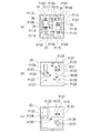
次に、図3ないし図6を参照して、高周波モジュール11の外観の一例について説明する。図3は高周波モジュール11の平面図である。図4は、図3における矢印A方向から見た高周波モジュール11の側面図である。図5は高周波モジュール11の底面図である。図6は、図3における矢印B方向から見た高周波モジュール11の側面図である。   Next, an example of the appearance of the high-frequency module 11 will be described with reference to FIGS. FIG. 3 is a plan view of the high-frequency module 11. FIG. 4 is a side view of the high-frequency module 11 viewed from the direction of arrow A in FIG. FIG. 5 is a bottom view of the high-frequency module 11. FIG. 6 is a side view of the high-frequency module 11 viewed from the direction of arrow B in FIG.

図3ないし図6に示したように、高周波モジュール11は、多層基板40と、この多層基板40の上面に実装された複数の部品41と、この部品41を覆うシールドケース42とを備えている。なお、図6は、シールドケース42を切り欠いて示している。多層基板40の外面には、外部回路に接続される接続端子として、アンテナ端子11aと、送信信号端子11bと、受信信号端子11cと、モニタ端子11dと、制御端子11eと、グランドに接続される3つのグランド端子11g,11h,11iが設けられている。部品41としては、例えば、ダイオード33,36、キャパシタ31および抵抗23,38がある。シールドケース42は金属によって形成されている。なお、部品41をシールドケース42によって覆う代わりに、部品41を成形された樹脂によって封止してもよい。   As shown in FIGS. 3 to 6, the high-frequency module 11 includes a multilayer substrate 40, a plurality of components 41 mounted on the upper surface of the multilayer substrate 40, and a shield case 42 that covers the components 41. . In FIG. 6, the shield case 42 is cut away. The outer surface of the multilayer substrate 40 is connected to an antenna terminal 11a, a transmission signal terminal 11b, a reception signal terminal 11c, a monitor terminal 11d, a control terminal 11e, and a ground as connection terminals connected to an external circuit. Three ground terminals 11g, 11h, and 11i are provided. Examples of the component 41 include diodes 33 and 36, a capacitor 31, and resistors 23 and 38. The shield case 42 is made of metal. Instead of covering the component 41 with the shield case 42, the component 41 may be sealed with a molded resin.

次に、図7ないし図12を参照して、多層基板40の構成の一例について説明する。この例では、多層基板40は、17層の誘電体層と、各誘電体層の上に形成された導体層またはマークを備えている。各誘電体層は、例えばセラミックによって形成される。図7において(a)、(b)、(c)は、それぞれ、上から1層目ないし3層目の誘電体層およびその上に形成された導体層を示している。図8において(a)、(b)、(c)は、それぞれ、上から4層目ないし6層目の誘電体層およびその上に形成された導体層を示している。図9において(a)、(b)、(c)は、それぞれ、上から7層目ないし9層目の誘電体層およびその上に形成された導体層を示している。図10において(a)、(b)、(c)は、それぞれ、上から10層目ないし12層目の誘電体層およびその上に形成された導体層を示している。図11において(a)、(b)、(c)は、それぞれ、上から13層目ないし15層目の誘電体層およびその上に形成された導体層を示している。図12において、(a)は、上から16層目の誘電体層およびその上に形成された導体層を示し、(b)は、上から17層目の誘電体層およびその上に形成されたマークを示している。なお、図7(b)、図8(a)〜(c)、図(a)〜(c)、図10(a)〜(c)、および図11(a)において、点線による円は、上の誘電体層に形成されたビアホールの位置を表している。   Next, an example of the configuration of the multilayer substrate 40 will be described with reference to FIGS. In this example, the multilayer substrate 40 includes 17 dielectric layers and a conductor layer or mark formed on each dielectric layer. Each dielectric layer is formed of ceramic, for example. In FIG. 7, (a), (b), and (c) respectively show the first to third dielectric layers from the top and the conductor layer formed thereon. In FIG. 8, (a), (b), and (c) respectively show the fourth to sixth dielectric layers from the top and the conductor layer formed thereon. In FIG. 9, (a), (b), and (c) respectively show the seventh to ninth dielectric layers from the top and the conductor layer formed thereon. In FIG. 10, (a), (b), and (c) show the tenth to twelfth dielectric layers from the top and the conductor layers formed thereon, respectively. In FIG. 11, (a), (b), and (c) respectively show the 13th to 15th dielectric layers from the top and the conductor layer formed thereon. In FIG. 12, (a) shows the 16th dielectric layer from above and the conductor layer formed thereon, and (b) shows the 17th dielectric layer from above and the dielectric layer formed thereon. Mark is shown. In addition, in FIG.7 (b), FIG.8 (a)-(c), figure (a)-(c), FIG.10 (a)-(c), and FIG. The position of the via hole formed in the upper dielectric layer is shown.

図7(a)に示した1層目の誘電体層51の上面には、導体層としての導体部P101〜P118が設けられている。導体部P101〜P108は、それぞれ、端子11a,11b,11c,11d,11e,11g,11h,11iに接続される。導体部P109,P110には、キャパシタ31の各端部が接続される。導体部P111,P112には、ダイオード33の各端部が接続される。導体部P113,P114には、ダイオード36の各端部が接続される。導体部P115,P116には、抵抗23の各端部が接続される。導体部P117,P118には、抵抗38の各端部が接続される。また、誘電体層51には、それぞれ導体部P109〜P118に接続された10個のビアホールが設けられている。図7(a)において、これらホールは、丸印で表わしている。   Conductor portions P101 to P118 as conductor layers are provided on the upper surface of the first dielectric layer 51 shown in FIG. The conductor portions P101 to P108 are connected to the terminals 11a, 11b, 11c, 11d, 11e, 11g, 11h, and 11i, respectively. Each end portion of the capacitor 31 is connected to the conductor portions P109 and P110. Each end of the diode 33 is connected to the conductor portions P111 and P112. Each end portion of the diode 36 is connected to the conductor portions P113 and P114. Each end portion of the resistor 23 is connected to the conductor portions P115 and P116. Each end portion of the resistor 38 is connected to the conductor portions P117 and P118. The dielectric layer 51 is provided with ten via holes connected to the conductor portions P109 to P118, respectively. In FIG. 7A, these holes are indicated by circles.

図7(b)に示した2層目の誘電体層52の上面には、導体層としての導体部P121〜P126が設けられている。また、誘電体層52には、ビアホールH121〜H127が設けられている。導体部P121は端子11aに接続される。また、導体部P121は、誘電体層51に設けられたビアホールを介して導体部P109に接続される。導体部P122は端子11eに接続される。また、導体部P122は、誘電体層51に設けられたビアホールを介して導体部P117に接続される。導体部P123は、誘電体層51に設けられたビアホールを介して、導体部P110,P111に接続される。また、導体部P123には、ビアホールH121,H122が接続されている。導体部P124は、キャパシタ35の一部を構成するものである。導体部P124は、誘電体層51に設けられたビアホールを介して導体部P113に接続される。また、導体部P124には、ビアホールH123が接続されている。導体部P125は、誘電体層51に設けられたビアホールを介して導体部P118に接続される。また、導体部P125には、ビアホールH124が接続されている。導体部P126は、誘電体層51に設けられたビアホールを介して導体部P115に接続される。また、導体部P126には、ビアホールH125が接続されている。ビアホールH126,H127は、それぞれ、誘電体層51に設けられたビアホールを介して、導体部P112,P116に接続される。   Conductor portions P121 to P126 as conductor layers are provided on the upper surface of the second dielectric layer 52 shown in FIG. 7B. The dielectric layer 52 is provided with via holes H121 to H127. The conductor part P121 is connected to the terminal 11a. The conductor part P121 is connected to the conductor part P109 through a via hole provided in the dielectric layer 51. The conductor part P122 is connected to the terminal 11e. The conductor part P122 is connected to the conductor part P117 through a via hole provided in the dielectric layer 51. The conductor part P123 is connected to the conductor parts P110 and P111 via via holes provided in the dielectric layer 51. In addition, via holes H121 and H122 are connected to the conductor portion P123. The conductor portion P124 constitutes a part of the capacitor 35. The conductor portion P124 is connected to the conductor portion P113 through a via hole provided in the dielectric layer 51. A via hole H123 is connected to the conductor portion P124. The conductor portion P125 is connected to the conductor portion P118 through a via hole provided in the dielectric layer 51. A via hole H124 is connected to the conductor portion P125. The conductor part P126 is connected to the conductor part P115 through a via hole provided in the dielectric layer 51. A via hole H125 is connected to the conductor portion P126. The via holes H126 and H127 are connected to the conductor parts P112 and P116 through via holes provided in the dielectric layer 51, respectively.

図7(c)に示した3層目の誘電体層53の上面には、導体層としての導体部P131〜P133が設けられている。また、誘電体層53には、ビアホールH131〜H137が設けられている。導体部P131には、ビアホールH131,H132が接続されている。ビアホールH131,H132は、それぞれ、ビアホールH121,H122に接続される。導体部P132は、キャパシタ35の一部を構成するものである。また、導体部P132は端子11cに接続される。導体部P133は、グランド用導体層を構成するものである。また、導体部P133は、端子11g、11h、11iに接続される。また、導体部P133は、ビアホールH127に接続される。また、導体部P133には、ビアホールH135が接続されている。ビアホールH133,H134,H136,H137は、それぞれ、ビアホールH123,H124,H125,H126に接続される。   Conductor portions P131 to P133 as conductor layers are provided on the top surface of the third dielectric layer 53 shown in FIG. The dielectric layer 53 is provided with via holes H131 to H137. Via holes H131 and H132 are connected to the conductor portion P131. The via holes H131 and H132 are connected to the via holes H121 and H122, respectively. The conductor portion P132 constitutes a part of the capacitor 35. Further, the conductor portion P132 is connected to the terminal 11c. The conductor part P133 constitutes a ground conductor layer. The conductor part P133 is connected to the terminals 11g, 11h, and 11i. The conductor part P133 is connected to the via hole H127. A via hole H135 is connected to the conductor portion P133. Via holes H133, H134, H136, and H137 are connected to via holes H123, H124, H125, and H126, respectively.

図8(a)に示した4層目の誘電体層54の上面には、導体層としての導体部P141,P142が設けられている。また、誘電体層54には、ビアホールH141〜H146が設けられている。導体部P141は、キャパシタ32の一部を構成するものである。また、導体部P141は、ビアホールH131に接続される。導体部P142は、キャパシタ35の一部を構成するものである。また、導体部P142には、ビアホールH142が接続されている。ビアホールH142は、ビアホールH133に接続される。ビアホールH141,H143,H144,H145,H146は、それぞれ、ビアホールH132,H134,H135,H136,H137に接続される。   Conductor portions P141 and P142 as conductor layers are provided on the upper surface of the fourth dielectric layer 54 shown in FIG. The dielectric layer 54 is provided with via holes H141 to H146. The conductor part P141 constitutes a part of the capacitor 32. The conductor part P141 is connected to the via hole H131. The conductor part P142 constitutes a part of the capacitor 35. A via hole H142 is connected to the conductor portion P142. The via hole H142 is connected to the via hole H133. Via holes H141, H143, H144, H145, and H146 are connected to via holes H132, H134, H135, H136, and H137, respectively.

図8(b)に示した5層目の誘電体層55の上面には、導体層としての導体部P151,P152が設けられている。また、誘電体層55には、ビアホールH151〜H156が設けられている。導体部P151は、グランド用導体層を構成するものである。また、導体部P151は端子11hに接続される。また、導体部P151には、ビアホールH154が接続されている。ビアホールH154は、ビアホールH144に接続される。導体部P152は、キャパシタ35の一部を構成するものである。また、導体部P152は端子11cに接続される。ビアホールH151,H152,H153,H155,H156は、それぞれ、ビアホールH141,H142,H143,H145,H146に接続される。   Conductor portions P151 and P152 as conductor layers are provided on the top surface of the fifth dielectric layer 55 shown in FIG. 8B. The dielectric layer 55 is provided with via holes H151 to H156. The conductor portion P151 constitutes a ground conductor layer. The conductor part P151 is connected to the terminal 11h. A via hole H154 is connected to the conductor portion P151. The via hole H154 is connected to the via hole H144. The conductor part P152 constitutes a part of the capacitor 35. The conductor portion P152 is connected to the terminal 11c. Via holes H151, H152, H153, H155, and H156 are connected to via holes H141, H142, H143, H145, and H146, respectively.

図8(c)に示した6層目の誘電体層56の上面には、導体層としての導体部P161,P162が設けられている。また、誘電体層56には、ビアホールH161〜H166が設けられている。導体部P161は、キャパシタ32の一部を構成するものである。また、導体部P161は、ビアホールH151に接続される。また、導体部P161には、ビアホールH161が接続されている。導体部P162は、キャパシタ35の一部を構成するものである。また、導体部P162には、ビアホールH162が接続されている。ビアホールH162は、ビアホールH152に接続される。ビアホールH163,H164,H165,H166は、それぞれ、ビアホールH153,H154,H155,H156に接続される。   Conductor portions P161 and P162 as conductor layers are provided on the top surface of the sixth dielectric layer 56 shown in FIG. The dielectric layer 56 is provided with via holes H161 to H166. The conductor portion P161 constitutes a part of the capacitor 32. The conductor part P161 is connected to the via hole H151. A via hole H161 is connected to the conductor portion P161. The conductor portion P162 constitutes a part of the capacitor 35. A via hole H162 is connected to the conductor portion P162. The via hole H162 is connected to the via hole H152. Via holes H163, H164, H165, and H166 are connected to via holes H153, H154, H155, and H156, respectively.

図9(a)に示した7層目の誘電体層57の上面には、導体層としての導体部P171,P172が設けられている。また、誘電体層57には、ビアホールH171〜H176が設けられている。導体部P171は、コイル34の一部を構成するものである。また、導体部P171の一端部は、ビアホールH161に接続される。また、導体部P171の他端部には、ビアホールH171が接続されている。導体部P172は、キャパシタ35の一部を構成するものである。また、導体部P172は端子11cに接続される。ビアホールH172,H173,H174,H175,H176は、それぞれ、ビアホールH162,H163,H164,H165,H166に接続される。   Conductor portions P171 and P172 as conductor layers are provided on the upper surface of the seventh dielectric layer 57 shown in FIG. The dielectric layer 57 is provided with via holes H171 to H176. The conductor portion P171 constitutes a part of the coil 34. In addition, one end portion of the conductor portion P171 is connected to the via hole H161. A via hole H171 is connected to the other end of the conductor part P171. The conductor portion P172 constitutes a part of the capacitor 35. The conductor portion P172 is connected to the terminal 11c. Via holes H172, H173, H174, H175, and H176 are connected to via holes H162, H163, H164, H165, and H166, respectively.

図9(b)に示した8層目の誘電体層58の上面には、導体層としての導体部P181が設けられている。また、誘電体層58には、ビアホールH181〜H186が設けられている。導体部P181は、コイル34の一部を構成するものである。また、導体部P181の一端部は、ビアホールH171に接続される。また、導体部P181の他端部には、ビアホールH181が接続されている。ビアホールH182,H183,H184,H185,H186は、それぞれ、ビアホールH172,H173,H174,H175,H176に接続される。   A conductor portion P181 as a conductor layer is provided on the upper surface of the eighth dielectric layer 58 shown in FIG. 9B. The dielectric layer 58 is provided with via holes H181 to H186. The conductor portion P181 constitutes a part of the coil 34. In addition, one end portion of the conductor portion P181 is connected to the via hole H171. A via hole H181 is connected to the other end of the conductor part P181. Via holes H182, H183, H184, H185, and H186 are connected to via holes H172, H173, H174, H175, and H176, respectively.

図9(c)に示した9層目の誘電体層59の上面には、導体層としての導体部P191,P192が設けられている。また、誘電体層59には、ビアホールH191〜H195が設けられている。導体部P191は、コイル34の一部を構成するものである。また、導体部P191の一端部は、ビアホールH181に接続される。また、導体部P191の他端部には、ビアホールH191が接続されている。導体部P192は、カプラ22の副ラインS2を構成するものである。また、導体部P192の一端部は、端子11dに接続される。また、導体部P192の他端部は、ビアホールH185に接続される。ビアホールH192,H193,H194,H195は、それぞれ、ビアホールH182,H183,H184,H186に接続される。   Conductor portions P191 and P192 as conductor layers are provided on the top surface of the ninth dielectric layer 59 shown in FIG. 9C. The dielectric layer 59 is provided with via holes H191 to H195. The conductor portion P191 constitutes a part of the coil 34. In addition, one end portion of the conductor portion P191 is connected to the via hole H181. A via hole H191 is connected to the other end of the conductor portion P191. The conductor portion P192 constitutes the sub line S2 of the coupler 22. One end of the conductor part P192 is connected to the terminal 11d. Further, the other end portion of the conductor portion P192 is connected to the via hole H185. Via holes H192, H193, H194, and H195 are connected to via holes H182, H183, H184, and H186, respectively.

図10(a)に示した10層目の誘電体層60の上面には、導体層としての導体部P201,P202が設けられている。また、誘電体層60には、ビアホールH201〜H204が設けられている。導体部P201は、コイル34の一部を構成するものである。また、導体部P201の一端部は、ビアホールH191に接続される。また、導体部P201の他端部には、ビアホールH201が接続されている。導体部P202は、カプラ22の主ラインS1を構成するものである。また、導体部P202の一端部は、端子11bに接続される。また、導体部P202の他端部は、ビアホールH195に接続される。ビアホールH202,H203,H204は、それぞれ、ビアホールH192,H193,H194に接続される。   Conductor portions P201 and P202 as conductor layers are provided on the top surface of the tenth dielectric layer 60 shown in FIG. The dielectric layer 60 is provided with via holes H201 to H204. The conductor portion P201 constitutes a part of the coil 34. In addition, one end portion of the conductor portion P201 is connected to the via hole H191. A via hole H201 is connected to the other end of the conductor part P201. The conductor portion P202 constitutes the main line S1 of the coupler 22. One end portion of the conductor portion P202 is connected to the terminal 11b. Further, the other end portion of the conductor portion P202 is connected to the via hole H195. Via holes H202, H203, and H204 are connected to via holes H192, H193, and H194, respectively.

図10(b)に示した11層目の誘電体層61の上面には、導体層としての導体部P211が設けられている。また、誘電体層61には、ビアホールH211,H212が設けられている。導体部P211は、コイル34の一部を構成するものである。また、導体部P211の一端部は、ビアホールH201に接続される。また、導体部P211の他端部は、ビアホールH202に接続される。ビアホールH211,H212は、それぞれ、ビアホールH203,H204に接続される。   A conductor portion P211 as a conductor layer is provided on the upper surface of the eleventh dielectric layer 61 shown in FIG. The dielectric layer 61 is provided with via holes H211 and H212. The conductor portion P211 constitutes a part of the coil 34. In addition, one end portion of the conductor portion P211 is connected to the via hole H201. Further, the other end portion of the conductor portion P211 is connected to the via hole H202. The via holes H211 and H212 are connected to the via holes H203 and H204, respectively.

図10(c)に示した12層目の誘電体層62には、ビアホールH221,H222が設けられている。ビアホールH221,H222は、ビアホールH211,H212に接続される。   Via holes H221 and H222 are provided in the twelfth dielectric layer 62 shown in FIG. The via holes H221 and H222 are connected to the via holes H211 and H212.

図11(a)に示した13層目の誘電体層63には、ビアホールH231,H232が設けられている。ビアホールH231,H232は、ビアホールH221,H222に接続される。   Via holes H231 and H232 are provided in the thirteenth dielectric layer 63 shown in FIG. Via holes H231 and H232 are connected to via holes H221 and H222.

図11(b)に示した14層目の誘電体層64の上面には、導体層としての導体部P241が設けられている。また、誘電体層64には、ビアホールH241が設けられている。導体部P241は、グランド用導体層を構成するものである。また、導体部P241は、端子11g,11h,11iに接続される。また、導体部P241は、ビアホールH232に接続される。ビアホールH241は、ビアホールH231に接続される。   A conductor portion P241 as a conductor layer is provided on the upper surface of the fourteenth dielectric layer 64 shown in FIG. The dielectric layer 64 is provided with a via hole H241. The conductor portion P241 constitutes a ground conductor layer. The conductor part P241 is connected to the terminals 11g, 11h, and 11i. The conductor part P241 is connected to the via hole H232. The via hole H241 is connected to the via hole H231.

図11(c)に示した15層目の誘電体層65の上面には、導体層としての導体部P251が設けられている。導体部P251は、キャパシタ37の一部を構成するものである。導体部P251は、ビアホールH241に接続される。   A conductor portion P251 as a conductor layer is provided on the top surface of the fifteenth dielectric layer 65 shown in FIG. The conductor portion P251 constitutes a part of the capacitor 37. The conductor part P251 is connected to the via hole H241.

図12(a)に示した16層目の誘電体層66の上面には、導体層としての導体部P261が設けられている。導体部P261は、グランド用導体層を構成するものである。また、導体部P261は、端子11g,11h,11iに接続される。   A conductor portion P261 as a conductor layer is provided on the upper surface of the sixteenth dielectric layer 66 shown in FIG. The conductor portion P261 constitutes a ground conductor layer. The conductor part P261 is connected to the terminals 11g, 11h, and 11i.

図12(b)に示した17層目の誘電体層67の上面には、マークP271が設けられている。   A mark P271 is provided on the upper surface of the seventeenth dielectric layer 67 shown in FIG.

多層基板40は、例えば、以下のようにして製造される。まず、ポリエチレンテレフタレートフィルム上にセラミックスラリーを塗布し、これを乾燥して、誘電体層となる誘電体シートを形成する。次に、この誘電体シートに、必要に応じて、ビアホール用の穴を形成する。次に、印刷工法によって、誘電体シート上に導電体ペーストを印刷して、所定のパターンの導体層を形成すると共に、導電体ペーストをビアホール用の穴に充填してビアホールを形成する。次に、このようにして導体層やビアホールが形成された複数枚の誘電体シートを、乾燥させた後、積み重ね、熱プレスによって一体化する。次に、このようにして得られた積層体を切断して、個々の多層基板40となる部分に分割する。次に、分割後の積層体を電気炉で焼成する。次に、この積層体の外周部に、外部回路に接続される接続端子を転写した後、これを焼成し、更に、これにめっきを施して、多層基板40が完成する。そして、この多層基板40に、部品41を実装し、更にシールドケース42を装着して、高周波モジュール11が完成する。   The multilayer substrate 40 is manufactured as follows, for example. First, a ceramic slurry is applied on a polyethylene terephthalate film and dried to form a dielectric sheet that becomes a dielectric layer. Next, holes for via holes are formed in the dielectric sheet as necessary. Next, a conductor paste is printed on the dielectric sheet by a printing method to form a conductor layer having a predetermined pattern, and the conductor paste is filled into the via hole to form a via hole. Next, the plurality of dielectric sheets on which the conductor layers and via holes are thus formed are dried, stacked, and integrated by hot pressing. Next, the laminated body obtained in this way is cut and divided into portions to be individual multilayer substrates 40. Next, the divided laminate is fired in an electric furnace. Next, after transferring the connection terminal connected to the external circuit to the outer peripheral portion of the laminated body, this is baked and further plated to complete the multilayer substrate 40. Then, the component 41 is mounted on the multilayer substrate 40, and the shield case 42 is further mounted, whereby the high frequency module 11 is completed.

このように、本実施の形態では、多層基板40を使用して高周波スイッチ21とカプラ22を一体化している。そのため、本実施の形態によれば、高周波スイッチ21とカプラ22を立体的に配置することができ、これにより、高周波スイッチ21とカプラ22を含む高周波モジュール11の小型化が可能になる。互いに別部品であった従来の高周波スイッチとカプラは、例えば次のような大きさであった。すなわち、高周波スイッチの大きさは、縦3.5mm、横3.5mm、高さ1.9mmである。カプラの大きさは、縦1.6mm、横0.8mm、高さ0.8mmである。これに対し、本実施の形態に係る高周波モジュール11は、高周波スイッチ21(抵抗38を含む。)、カプラ22および抵抗23を含みながら、例えば、従来の単体の高周波スイッチと同じ、縦3.5mm、横3.5mm、高さ1.9mmという大きさにすることができる。   Thus, in the present embodiment, the high frequency switch 21 and the coupler 22 are integrated using the multilayer substrate 40. For this reason, according to the present embodiment, the high-frequency switch 21 and the coupler 22 can be three-dimensionally arranged, whereby the high-frequency module 11 including the high-frequency switch 21 and the coupler 22 can be downsized. Conventional high-frequency switches and couplers, which are separate parts, have the following sizes, for example. That is, the size of the high-frequency switch is 3.5 mm in length, 3.5 mm in width, and 1.9 mm in height. The size of the coupler is 1.6 mm in length, 0.8 mm in width, and 0.8 mm in height. In contrast, the high-frequency module 11 according to the present embodiment includes the high-frequency switch 21 (including the resistor 38), the coupler 22, and the resistor 23. , Width 3.5 mm, height 1.9 mm.

本実施の形態では、高周波モジュール11に含まれる受動素子の少なくとも一部を、多層基板40に内蔵している。また、本実施の形態では、多層基板40に内蔵したスイッチの受動素子として、分布定数回路素子ではなく、コイルやキャパシタといった集中定数回路素子を使用した。分布定数回路素子では、例えば信号の波長の1/4といった、信号の波長に依存した長さが必要になる。そのため、受動素子として分布定数回路素子を用いると、多層基板40の小型化が難しくなる場合がある。これに対し、本実施の形態では、受動素子として集中定数回路素子を使用したので、多層基板40の小型化が可能になる。   In the present embodiment, at least a part of the passive elements included in the high-frequency module 11 is built in the multilayer substrate 40. Further, in the present embodiment, a lumped constant circuit element such as a coil or a capacitor is used as a passive element of a switch built in the multilayer substrate 40 instead of a distributed constant circuit element. The distributed constant circuit element requires a length depending on the signal wavelength, for example, ¼ of the signal wavelength. Therefore, when a distributed constant circuit element is used as a passive element, it may be difficult to reduce the size of the multilayer substrate 40. On the other hand, in the present embodiment, since the lumped constant circuit element is used as the passive element, the multilayer substrate 40 can be downsized.

本実施の形態では、前述のように、カプラ22の結合度Cを−XdB、カプラ22の方向性Dを−YdBとしたとき、Xを10〜21の範囲内とし、Yを21以上、好ましくは23以上としている。このようなカプラ22の特性を実現するには、特に、カプラ22の方向性の改善、すなわちYを大きくすることが必要である。以下、本実施の形態におけるカプラ22の特性を実現する方法について説明する。本実施の形態のようにストリップラインを用いたカプラ22の場合、原理的に、ストリップラインの特性インピーダンスが負荷抵抗に等しいときに最もカプラ22と負荷との間における信号の反射が少なく、カプラ22の損失も少ない。また、原理的に、主ラインS1と副ラインS2が対向している領域の長さが、信号の波長の1/4に等しいときに、アイソレートポートP4に信号が発生せず、カプラ22の方向性がよくなる。しかし、積層体内に形成される実際のカプラ22の場合には、理想的なストリップラインの設計が困難であることや、カプラ22に接続される部品の入出力インピーダンスがストリップラインの特性インピーダンス(例えば50Ω)に等しいとは限らないので反射が生じることにより、アイソレートポートP4へ信号が漏れ、カプラ22の方向性を十分に大きくすることが難しい。   In the present embodiment, as described above, when the coupling degree C of the coupler 22 is −X dB and the directivity D of the coupler 22 is −Y dB, X is in the range of 10 to 21, and Y is 21 or more, preferably Is 23 or more. In order to realize such characteristics of the coupler 22, it is particularly necessary to improve the directionality of the coupler 22, that is, to increase Y. Hereinafter, a method for realizing the characteristics of the coupler 22 in the present embodiment will be described. In the case of the coupler 22 using the strip line as in the present embodiment, in principle, when the characteristic impedance of the strip line is equal to the load resistance, the reflection of the signal between the coupler 22 and the load is the least, and the coupler 22 There is little loss. Further, in principle, when the length of the region where the main line S1 and the sub line S2 are opposed is equal to ¼ of the signal wavelength, no signal is generated at the isolated port P4, and the coupler 22 Directionality is improved. However, in the case of the actual coupler 22 formed in the laminated body, it is difficult to design an ideal strip line, and the input / output impedance of components connected to the coupler 22 is the characteristic impedance of the strip line (for example, Therefore, it is difficult to make the direction of the coupler 22 sufficiently large because reflection occurs and a signal leaks to the isolated port P4.

そこで、カプラ22の方向性を大きく(Yを大きく)するために、カプラ22を構成するストリップラインの特性インピーダンスを変えることを考える。ここでは、カプラ22の主ラインS1と副ラインS2がそれぞれ、トリプレートストリップラインにおける中心の導体層によって構成されるものとする。そして、トリプレートストリップラインにおける上下の2つのグランド用導体層の間の距離を一定とし、中心の導体層の幅を調整することで、ストリップラインの特性インピーダンスを変化させることを考える。   Therefore, in order to increase the directionality of the coupler 22 (increase Y), consider changing the characteristic impedance of the strip line constituting the coupler 22. Here, it is assumed that the main line S1 and the sub line S2 of the coupler 22 are each constituted by a central conductor layer in the triplate strip line. Then, let us consider changing the characteristic impedance of the stripline by adjusting the width of the central conductor layer while keeping the distance between the upper and lower two ground conductor layers in the triplate stripline constant.

カプラ22の主ラインS1は送信回路へ接続されるため、その出力インピーダンスは例えば50Ωに整合している必要がある。そのため、主ラインS1の幅を変更することは好ましくない。これに対し、副ラインS2は、送信信号の検出に用いられるだけなので、特性インピーダンスを変化させることが可能である。そこで、本実施の形態では、副ラインS2の幅を主ラインS1の幅よりも小さくして、副ラインS2の特性インピーダンスを大きくし、これにより、主ラインS1から副ラインS2のアイソレートポートP4への信号の漏れを抑制する。   Since the main line S1 of the coupler 22 is connected to the transmission circuit, its output impedance needs to be matched to, for example, 50Ω. Therefore, it is not preferable to change the width of the main line S1. On the other hand, since the sub line S2 is only used for detection of the transmission signal, the characteristic impedance can be changed. Therefore, in the present embodiment, the width of the sub-line S2 is made smaller than the width of the main line S1, and the characteristic impedance of the sub-line S2 is increased, whereby the isolated port P4 from the main line S1 to the sub-line S2. Suppresses signal leakage to

副ラインS2の幅を小さくすると、カプラ22の結合が弱く(Xが大きく)なるが、主ラインS1と副ラインS2が対向している領域の長さを大きくすることで、カプラ22の結合が弱くなることを防止できる。主ラインS1と副ラインS2が対向している領域の長さを大きくしても、各ラインS1,S2の特性インピーダンスの関係は変わらないので、アイソレートポートP4への信号の漏れは増加しない。   When the width of the sub line S2 is reduced, the coupling of the coupler 22 is weakened (X is increased). However, by increasing the length of the region where the main line S1 and the sub line S2 face each other, the coupling of the coupler 22 is reduced. It can prevent weakening. Even if the length of the region where the main line S1 and the subline S2 are opposed to each other is increased, the relationship between the characteristic impedances of the respective lines S1 and S2 does not change, and therefore the signal leakage to the isolated port P4 does not increase.

上述のように、副ラインS2の幅を主ラインS1の幅よりも小さくすることによりカプラ22の方向性およびアイソレーションを改善することができる。しかし、印刷工程において実現可能なライン幅には最小値が存在することから、副ラインS2の幅を小さくすることには限界がある。そのため、この製造上の制約とカプラの特性改善の要求との兼ね合いで、副ラインS2の幅を主ラインS1の幅で除した値は、0.9〜0.2の範囲内であることが好ましい。主ラインS1の特性インピーダンスを50Ωとした場合、副ラインS2の幅を主ラインS1の幅で除した値が0.9〜0.2の範囲内であるとき、副ラインS2の特性インピーダンスは、およそ54〜80Ωの範囲内となる。   As described above, the directionality and isolation of the coupler 22 can be improved by making the width of the sub-line S2 smaller than the width of the main line S1. However, since there is a minimum value for the line width that can be realized in the printing process, there is a limit to reducing the width of the sub-line S2. For this reason, the value obtained by dividing the width of the sub-line S2 by the width of the main line S1 may be in the range of 0.9 to 0.2 in consideration of the manufacturing restrictions and the demand for improving the characteristics of the coupler. preferable. When the characteristic impedance of the main line S1 is 50Ω, when the value obtained by dividing the width of the subline S2 by the width of the main line S1 is in the range of 0.9 to 0.2, the characteristic impedance of the subline S2 is It is in the range of approximately 54-80Ω.

このように、副ラインS2の幅を主ラインS1の幅よりも小さくすることによりカプラ22の方向性およびアイソレーションを改善することができるが、まだ十分とは言えない。そこで、次に、副ラインS2のアイソレートポートP4に接続される終端抵抗23について考える。前述のように、副ラインS2の特性インピーダンスを変化させることで、カプラ22の方向性およびアイソレーションを改善することができる。更に考えると、終端抵抗23の抵抗値を変化させることにより、主ラインS1から見た副ラインS2のインピーダンスを変化させることが可能であることから、終端抵抗23の抵抗値を変化させることによっても、カプラ22の方向性およびアイソレーションを改善することが可能である。ただし、終端抵抗23の抵抗値を変化させると、モニタポートP3の出力インピーダンスが大きく変化するので、終端抵抗23の抵抗値の変化量には限界がある。   As described above, the directionality and isolation of the coupler 22 can be improved by making the width of the sub-line S2 smaller than the width of the main line S1, but it is not yet sufficient. Then, next, consider the termination resistor 23 connected to the isolated port P4 of the sub line S2. As described above, the directionality and isolation of the coupler 22 can be improved by changing the characteristic impedance of the sub-line S2. Considering further, it is possible to change the impedance of the sub-line S2 as viewed from the main line S1 by changing the resistance value of the termination resistor 23. Therefore, it is also possible to change the resistance value of the termination resistor 23. It is possible to improve the directivity and isolation of the coupler 22. However, if the resistance value of the termination resistor 23 is changed, the output impedance of the monitor port P3 changes greatly, so that the amount of change in the resistance value of the termination resistor 23 is limited.

通常、単体のカプラは、特性インピーダンスが50Ωの系での使用に対して最適化されているため、カプラに対して外付けする終端抵抗には、抵抗値50Ωのものが用いられる。しかし、本実施の形態では、終端抵抗23を、カプラ22と共に高周波モジュール11に一体化している。そのため、本実施の形態では、副ラインS2の特性インピーダンスとの組み合わせで、終端抵抗23の抵抗値を最適化することによって、カプラ22の方向性およびアイソレーションを改善することができる。   Usually, a single coupler is optimized for use in a system having a characteristic impedance of 50Ω, so that a termination resistor externally attached to the coupler has a resistance value of 50Ω. However, in the present embodiment, the termination resistor 23 is integrated with the high frequency module 11 together with the coupler 22. Therefore, in this embodiment, the directionality and isolation of the coupler 22 can be improved by optimizing the resistance value of the termination resistor 23 in combination with the characteristic impedance of the sub line S2.

終端抵抗23の抵抗値の最適化は、例えば、以下のようにして行なうことができる。まず、カプラ22の構造シミュレーションを行って、カプラ22の特性をSパラメータで出力する。次に、回路シミュレータによって、構造シミュレーションの結果に終端抵抗23の抵抗値を追加して、カプラ22の特性をシミュレートする。このとき、カプラ22の特性を悪化させない範囲、例えば、モニタポートP3における反射損失が10dB以上となる範囲で、終端抵抗23の抵抗値を変化させて、カプラ22のアイソレーション(Zの値)が最大になるように、終端抵抗23の抵抗値を最適化する。そして、このシミュレーションによって得られた終端抵抗23の抵抗値を、実際の終端抵抗23の抵抗値とする。   The optimization of the resistance value of the termination resistor 23 can be performed as follows, for example. First, a structure simulation of the coupler 22 is performed, and the characteristics of the coupler 22 are output as S parameters. Next, the resistance value of the termination resistor 23 is added to the result of the structure simulation by the circuit simulator to simulate the characteristics of the coupler 22. At this time, the resistance (Z value) of the coupler 22 is changed by changing the resistance value of the termination resistor 23 in a range where the characteristics of the coupler 22 are not deteriorated, for example, in a range where the reflection loss at the monitor port P3 is 10 dB or more. The resistance value of the termination resistor 23 is optimized so as to be maximized. Then, the resistance value of the termination resistor 23 obtained by this simulation is used as the actual resistance value of the termination resistor 23.

前述のように、副ラインS2の幅を主ラインS1の幅で除した値が0.9〜0.2の範囲内で、副ラインS2の特性インピーダンスがおよそ54〜80Ωの範囲内である場合、最適な終端抵抗23の抵抗値は、例えばおよそ30〜47Ωの範囲内となる。   As described above, when the value obtained by dividing the width of the subline S2 by the width of the main line S1 is in the range of 0.9 to 0.2, and the characteristic impedance of the subline S2 is in the range of about 54 to 80Ω. The optimum resistance value of the termination resistor 23 is, for example, in the range of about 30 to 47Ω.

なお、ここまでは、副ラインS2の幅を変えることで、副ラインS2の特性インピーダンスを変化させる場合について説明してきたが、トリプレートストリップラインにおける上下の2つのグランド用導体層の間の距離を変えることによっても、副ラインS2の特性インピーダンスを変化させることが可能である。   Up to this point, the case where the characteristic impedance of the sub-line S2 is changed by changing the width of the sub-line S2 has been described. However, the distance between the upper and lower ground conductor layers in the triplate strip line is set as follows. It is possible to change the characteristic impedance of the sub-line S2 also by changing it.

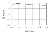
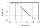
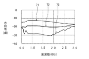
次に、図13ないし図16を参照して、本実施の形態に係る高周波モジュール11の特性の一例について説明する。図13は、高周波モジュール11の送信時における送信信号の経路の挿入損失の周波数特性を示している。図14は、高周波モジュール11の受信時における受信信号の経路の挿入損失の周波数特性を示している。図15は、カプラ22の結合度の周波数特性を示している。図16は、カプラ22の方向性の周波数特性を示している。図13ないし図16は、0.8〜0.9GHzの周波数帯域での使用に適するように設計された例を示している。   Next, an example of the characteristics of the high-frequency module 11 according to the present embodiment will be described with reference to FIGS. FIG. 13 shows the frequency characteristics of the insertion loss of the transmission signal path during transmission of the high-frequency module 11. FIG. 14 shows the frequency characteristics of the insertion loss of the path of the received signal at the time of reception by the high frequency module 11. FIG. 15 shows the frequency characteristics of the degree of coupling of the coupler 22. FIG. 16 shows the directional frequency characteristics of the coupler 22. FIGS. 13 to 16 show examples designed to be suitable for use in the frequency band of 0.8 to 0.9 GHz.

この例では、図15に示したように、上記の使用周波数帯域において、カプラ22の結合度は−19〜−21dBの範囲内となっている。   In this example, as shown in FIG. 15, the coupling degree of the coupler 22 is within a range of −19 to −21 dB in the above-described use frequency band.

図16において、符号71は、主ラインS1の幅と副ラインS2の幅を等しくした場合におけるカプラ22の方向性を表している。また、符号72は、副ラインS2の幅を主ラインS1の幅で除した値を0.5とし、副ラインS2の特性インピーダンスを63Ωとしたが、終端抵抗23の抵抗値の最適化を行なわずに、終端抵抗23の抵抗値を51Ωとした場合におけるカプラ22の方向性を表している。また、符号73は、副ラインS2の幅を主ラインS1の幅で除した値を0.5とし、副ラインS2の特性インピーダンスを63Ωとし、更に、終端抵抗23の抵抗値の最適化を行なって、終端抵抗23の抵抗値を36Ωとした場合におけるカプラ22の方向性を表している。   In FIG. 16, reference numeral 71 represents the directivity of the coupler 22 when the width of the main line S1 is equal to the width of the subline S2. Reference numeral 72 denotes a value obtained by dividing the width of the sub-line S2 by the width of the main line S1 to 0.5 and the characteristic impedance of the sub-line S2 to 63Ω, but the resistance value of the termination resistor 23 is optimized. The directionality of the coupler 22 when the resistance value of the termination resistor 23 is 51Ω is shown. Reference numeral 73 denotes a value obtained by dividing the width of the sub-line S2 by the width of the main line S1, 0.5, the characteristic impedance of the sub-line S2 is 63Ω, and the resistance value of the termination resistor 23 is optimized. Thus, the directionality of the coupler 22 when the resistance value of the termination resistor 23 is 36Ω is shown.

図16から分かるように、副ラインS2の幅を主ラインS1の幅よりも小さくすることによりカプラ22の方向性を改善することができるが、まだ十分とは言えない。しかし、更に、終端抵抗23の抵抗値の最適化を行なうことにより、カプラ22の方向性をより改善することができ、使用周波数帯域において、カプラ22の方向性を−YdBとしたときにYが23以上となる特性を得ることができた。この例では、使用周波数帯域において、Yは、27〜29の範囲内となっている。   As can be seen from FIG. 16, the directivity of the coupler 22 can be improved by making the width of the sub-line S2 smaller than the width of the main line S1, but this is not yet sufficient. However, by further optimizing the resistance value of the termination resistor 23, the directivity of the coupler 22 can be further improved, and when the directivity of the coupler 22 is -YdB in the operating frequency band, Y is The characteristic which becomes 23 or more was able to be acquired. In this example, Y is in the range of 27 to 29 in the used frequency band.

なお、上記の例におけるカプラ22のアイソレーションの周波数特性は図示していないが、前述のように、アイソレーションは、方向性+結合度として求められる。   In addition, although the frequency characteristic of isolation of the coupler 22 in the above example is not illustrated, the isolation is obtained as directionality + coupling degree as described above.

以上説明したように、本実施の形態によれば、高周波モジュール11によって高周波スイッチ21とカプラ22を一体化でき、その結果、高周波回路の小型化、軽量化が可能になる。また、本実施の形態によれば、カプラ22において十分なアイソレーションを確保することができる。   As described above, according to this embodiment, the high frequency switch 11 and the coupler 22 can be integrated by the high frequency module 11, and as a result, the high frequency circuit can be reduced in size and weight. Further, according to the present embodiment, sufficient isolation can be secured in the coupler 22.

[第2の実施の形態]
次に、図17および図18を参照して、本発明の第2の実施の形態に係る高周波モジュールおよび高周波回路について説明する。図17は、本実施の形態に係る高周波回路の構成を示すブロック図である。図18は、本実施の形態に係る高周波モジュールの回路構成の一例を示す回路図である。
[Second Embodiment]
Next, with reference to FIG. 17 and FIG. 18, the high frequency module and high frequency circuit which concern on the 2nd Embodiment of this invention are demonstrated. FIG. 17 is a block diagram showing the configuration of the high-frequency circuit according to the present embodiment. FIG. 18 is a circuit diagram illustrating an example of a circuit configuration of the high-frequency module according to the present embodiment.

図17に示したように、本実施の形態に係る高周波モジュール11は、送信信号端子11bと高周波スイッチ21の間に設けられ、送信信号のうちの不要な信号成分を抑制するフィルタ24を備えている。フィルタ24は、具体的には、カプラ22の出力ポートP2と高周波スイッチ21の送信信号ポート21bとの間に設けられている。また、本実施の形態では、アイソレータ13は設けられておらず、電力増幅器12の出力端が高周波モジュール11の送信信号端子11bに接続されている。   As shown in FIG. 17, the high-frequency module 11 according to the present embodiment includes a filter 24 that is provided between the transmission signal terminal 11b and the high-frequency switch 21 and suppresses unnecessary signal components of the transmission signal. Yes. Specifically, the filter 24 is provided between the output port P2 of the coupler 22 and the transmission signal port 21b of the high frequency switch 21. In the present embodiment, the isolator 13 is not provided, and the output terminal of the power amplifier 12 is connected to the transmission signal terminal 11 b of the high-frequency module 11.

フィルタ24は、LPF、BPFのいずれであってもよい。また、フィルタ24は、例えば、弾性波素子を用いて構成されていてもよい。弾性波素子は、弾性表面波素子でもよいし、バルク弾性波素子でもよい。   The filter 24 may be either LPF or BPF. The filter 24 may be configured using, for example, an acoustic wave element. The acoustic wave element may be a surface acoustic wave element or a bulk acoustic wave element.

図18は、フィルタ24をLPFとした場合における高周波モジュール11の回路構成の一例を示している。この場合、フィルタ24は、送信信号における高調波成分を減衰させる機能を有する。この例では、フィルタ24は、カプラ22の出力ポートP2と高周波スイッチ21のダイオード33のカソードとの間に設けられている。フィルタ24は、一端が出力ポートP2に接続され、他端がダイオード33のカソードに接続されたコイル81と、一端が出力ポートP2に接続され、他端がダイオード33のカソードに接続されたキャパシタ82と、一端が出力ポートP2に接続されたコイル83と、一端がコイル83の他端に接続され、他端が接地されたキャパシタ84と、一端がダイオード33のカソードに接続され、他端が接地されたキャパシタ85とを有している。   FIG. 18 shows an example of the circuit configuration of the high-frequency module 11 when the filter 24 is an LPF. In this case, the filter 24 has a function of attenuating harmonic components in the transmission signal. In this example, the filter 24 is provided between the output port P <b> 2 of the coupler 22 and the cathode of the diode 33 of the high frequency switch 21. The filter 24 has one end connected to the output port P2 and the other end connected to the cathode of the diode 33, and a capacitor 82 having one end connected to the output port P2 and the other end connected to the cathode of the diode 33. A coil 83 having one end connected to the output port P2, a capacitor 84 having one end connected to the other end of the coil 83 and the other end grounded, one end connected to the cathode of the diode 33, and the other end grounded The capacitor 85 is provided.

本実施の形態において、フィルタ24の構成要素は、多層基板40の導体層を用いて構成され、多層基板40に一体化されている。本実施の形態では、第1の実施の形態と比較して、高周波モジュール11の構成要素としてフィルタ24が追加されるが、高周波モジュール11の大きさはそれほど変わることはない。一方、本実施の形態では、第1の実施の形態と比較して、アイソレータ13が除かれるため、高周波回路を、より小型化、軽量化することができる。   In the present embodiment, the constituent elements of the filter 24 are configured using the conductor layer of the multilayer substrate 40 and are integrated with the multilayer substrate 40. In the present embodiment, the filter 24 is added as a component of the high frequency module 11 as compared with the first embodiment, but the size of the high frequency module 11 does not change so much. On the other hand, in the present embodiment, as compared with the first embodiment, the isolator 13 is removed, so that the high-frequency circuit can be further reduced in size and weight.

本実施の形態におけるその他の構成、作用および効果は、第1の実施の形態と同様である。   Other configurations, operations, and effects in the present embodiment are the same as those in the first embodiment.

[第3の実施の形態]
次に、図19を参照して、本発明の第3の実施の形態に係る高周波モジュールおよび高周波回路について説明する。図19は、本実施の形態に係る高周波回路の構成を示すブロック図である。
[Third Embodiment]
Next, a high frequency module and a high frequency circuit according to the third embodiment of the present invention will be described with reference to FIG. FIG. 19 is a block diagram showing a configuration of the high-frequency circuit according to the present embodiment.

本実施の形態では、高周波モジュール11が、第2の実施の形態における構成要素に加え、電力増幅器12およびAPC回路14を含んでいる。本実施の形態に係る高周波モジュール11は、第2の実施の形態における送信信号端子11bおよびモニタ端子11dを備えておらず、代わりに送信信号端子11fを備えている。送信信号端子11fは、高周波回路の送信信号端子2と電力増幅器12の入力端とに接続されている。電力増幅器12の出力端は、カプラ22の入力ポートP1に接続されている。APC回路14の入力端は、カプラ22のモニタポートP3に接続されている。   In the present embodiment, the high frequency module 11 includes a power amplifier 12 and an APC circuit 14 in addition to the components in the second embodiment. The high-frequency module 11 according to the present embodiment does not include the transmission signal terminal 11b and the monitor terminal 11d in the second embodiment, but includes a transmission signal terminal 11f instead. The transmission signal terminal 11 f is connected to the transmission signal terminal 2 of the high frequency circuit and the input terminal of the power amplifier 12. The output terminal of the power amplifier 12 is connected to the input port P 1 of the coupler 22. The input end of the APC circuit 14 is connected to the monitor port P3 of the coupler 22.

電力増幅器12およびAPC回路14は、能動素子と受動素子とを含んでいる。能動素子は、多層基板40に搭載される。受動素子の少なくとも一部は、多層基板40の導体層を用いて構成されていてもよい。多層基板40の導体層を用いて構成されない受動素子は、多層基板40に搭載される。   The power amplifier 12 and the APC circuit 14 include active elements and passive elements. The active element is mounted on the multilayer substrate 40. At least a part of the passive element may be configured using the conductor layer of the multilayer substrate 40. Passive elements that are not configured using the conductor layers of the multilayer substrate 40 are mounted on the multilayer substrate 40.

本実施の形態によれば、高周波回路を、より小型化、軽量化することができる。本実施の形態におけるその他の構成、作用および効果は、第2の実施の形態と同様である。なお、本実施の形態を変形して、電力増幅器12とAPC回路14のうち、電力増幅器12のみを高周波モジュール11に含めてもよい。   According to the present embodiment, the high-frequency circuit can be further reduced in size and weight. Other configurations, operations, and effects in the present embodiment are the same as those in the second embodiment. It should be noted that only the power amplifier 12 of the power amplifier 12 and the APC circuit 14 may be included in the high-frequency module 11 by modifying this embodiment.

なお、本発明は、上記各実施の形態に限定されず、種々の変更が可能である。例えば、積層体は、誘電体層がセラミックよりなる多層基板に限らず、誘電体層が樹脂よりなる基板であってもよい。   In addition, this invention is not limited to said each embodiment, A various change is possible. For example, the laminate is not limited to a multilayer substrate in which the dielectric layer is made of ceramic, but may be a substrate in which the dielectric layer is made of resin.

本発明の第1の実施の形態に係る移動体通信機器用高周波回路の構成を示すブロック図である。It is a block diagram which shows the structure of the high frequency circuit for mobile communication apparatuses which concerns on the 1st Embodiment of this invention. 本発明の第1の実施の形態に係る高周波モジュールの回路構成の一例を示す回路図である。It is a circuit diagram showing an example of circuit composition of a high frequency module concerning a 1st embodiment of the present invention. 本発明の第1の実施の形態に係る高周波モジュールの平面図である。It is a top view of the high frequency module concerning a 1st embodiment of the present invention. 図3における矢印A方向から見た高周波モジュールの側面図である。It is the side view of the high frequency module seen from the arrow A direction in FIG. 図3に示した高周波モジュールの底面図である。FIG. 4 is a bottom view of the high frequency module shown in FIG. 3. 図3における矢印B方向から見た高周波モジュールの側面図である。It is the side view of the high frequency module seen from the arrow B direction in FIG. 本発明の第1の実施の形態における多層基板の構成の一例を示す説明図である。It is explanatory drawing which shows an example of a structure of the multilayer substrate in the 1st Embodiment of this invention. 本発明の第1の実施の形態における多層基板の構成の一例を示す説明図である。It is explanatory drawing which shows an example of a structure of the multilayer substrate in the 1st Embodiment of this invention. 本発明の第1の実施の形態における多層基板の構成の一例を示す説明図である。It is explanatory drawing which shows an example of a structure of the multilayer substrate in the 1st Embodiment of this invention. 本発明の第1の実施の形態における多層基板の構成の一例を示す説明図である。It is explanatory drawing which shows an example of a structure of the multilayer substrate in the 1st Embodiment of this invention. 本発明の第1の実施の形態における多層基板の構成の一例を示す説明図である。It is explanatory drawing which shows an example of a structure of the multilayer substrate in the 1st Embodiment of this invention. 本発明の第1の実施の形態における多層基板の構成の一例を示す説明図である。It is explanatory drawing which shows an example of a structure of the multilayer substrate in the 1st Embodiment of this invention. 本発明の第1の実施の形態に係る高周波モジュールの送信時における送信信号の経路の挿入損失の周波数特性を示す特性図である。It is a characteristic view which shows the frequency characteristic of the insertion loss of the path | route of the transmission signal at the time of transmission of the high frequency module which concerns on the 1st Embodiment of this invention. 本発明の第1の実施の形態に係る高周波モジュールの受信時における受信信号の経路の挿入損失の周波数特性を示す特性図である。It is a characteristic view which shows the frequency characteristic of the insertion loss of the path | route of the received signal at the time of reception of the high frequency module which concerns on the 1st Embodiment of this invention. 本発明の第1の実施の形態におけるカプラの結合度の周波数特性を示す特性図である。It is a characteristic view which shows the frequency characteristic of the coupling degree of the coupler in the 1st Embodiment of this invention. 本発明の第1の実施の形態におけるカプラの方向性の周波数特性を示す特性図である。It is a characteristic view which shows the frequency characteristic of the directionality of the coupler in the 1st Embodiment of this invention. 本発明の第2の実施の形態に係る移動体通信機器用高周波回路の構成を示すブロック図である。It is a block diagram which shows the structure of the high frequency circuit for mobile communication apparatuses which concerns on the 2nd Embodiment of this invention. 本発明の第2の実施の形態に係る高周波モジュールの回路構成の一例を示す回路図である。It is a circuit diagram which shows an example of the circuit structure of the high frequency module which concerns on the 2nd Embodiment of this invention. 本発明の第3の実施の形態に係る移動体通信機器用高周波回路の構成を示すブロック図である。It is a block diagram which shows the structure of the high frequency circuit for mobile communication apparatuses which concerns on the 3rd Embodiment of this invention. 移動体通信機器における高周波回路の構成の一例を示すブロック図である。It is a block diagram which shows an example of a structure of the high frequency circuit in a mobile communication apparatus.

符号の説明Explanation of symbols

1…アンテナ、2…送信信号端子、3…受信信号端子、11…高周波モジュール、21…高周波スイッチ、22…方向性結合器、23…終端抵抗。
DESCRIPTION OF SYMBOLS 1 ... Antenna, 2 ... Transmission signal terminal, 3 ... Reception signal terminal, 11 ... High frequency module, 21 ... High frequency switch, 22 ... Directional coupler, 23 ... Termination resistor.

Claims (12)

アンテナに接続されるアンテナ端子と、
送信信号が入力される送信信号端子と、
受信信号を出力する受信信号端子と、
前記アンテナ端子に対して前記送信信号端子と受信信号端子のいずれかを選択的に接続する高周波スイッチと、
前記送信信号端子と前記高周波スイッチの間に設けられ、前記送信信号を検出する方向性結合器と、
交互に積層された誘電体層と導体層とを含む積層体とを備え、
前記積層体によって構成要素が一体化された高周波モジュールであって、
前記方向性結合器は、前記誘電体層を挟んで対向する主ラインと副ラインとを有し、
前記主ラインは、前記送信信号端子と前記高周波スイッチとの間の信号経路に挿入され、
前記副ラインは、前記主ラインよりも狭い幅を有し、
高周波モジュールは、更に、前記副ラインの一端に接続された終端抵抗を備え、
前記方向性結合器の結合度を−XdB、前記方向性結合器の方向性を−YdBとしたとき、Xは10〜21の範囲内であり、Yは21以上であることを特徴とする高周波モジュール。
An antenna terminal connected to the antenna;
A transmission signal terminal to which a transmission signal is input; and
A reception signal terminal for outputting a reception signal;
A high-frequency switch that selectively connects either the transmission signal terminal or the reception signal terminal to the antenna terminal;
A directional coupler provided between the transmission signal terminal and the high-frequency switch for detecting the transmission signal;
A laminate including alternately laminated dielectric layers and conductor layers;
A high-frequency module in which components are integrated by the laminate,
The directional coupler has a main line and a sub line facing each other across the dielectric layer,
The main line is inserted in a signal path between the transmission signal terminal and the high frequency switch,
The sub-line has a narrower width than the main line,
The high-frequency module further includes a termination resistor connected to one end of the sub line,
When the coupling degree of the directional coupler is −X dB and the directionality of the directional coupler is −Y dB, X is in the range of 10 to 21, and Y is 21 or more. module.
Yは23以上であることを特徴とする請求項1記載の高周波モジュール。   The high-frequency module according to claim 1, wherein Y is 23 or more. 前記副ラインの特性インピーダンスは、前記主ラインの特性インピーダンスよりも大きいことを特徴とする請求項1または2記載の高周波モジュール。   The high frequency module according to claim 1 or 2, wherein the characteristic impedance of the sub line is larger than the characteristic impedance of the main line. 前記終端抵抗は前記積層体に搭載されていることを特徴とする請求項1ないし3のいずれかに記載の高周波モジュール。   The high-frequency module according to claim 1, wherein the termination resistor is mounted on the laminated body. 前記高周波スイッチは能動素子と受動素子とを含み、
前記能動素子は前記積層体に搭載され、
前記受動素子の少なくとも一部は、前記導体層を用いて構成されていることを特徴とする請求項1ないし4のいずれかに記載の高周波モジュール。
The high frequency switch includes an active element and a passive element,
The active element is mounted on the laminate,
The high-frequency module according to claim 1, wherein at least a part of the passive element is configured using the conductor layer.
前記能動素子はダイオードであることを特徴とする請求項5記載の高周波モジュール。   The high-frequency module according to claim 5, wherein the active element is a diode. 前記導体層を用いて構成された受動素子は、集中定数素子であることを特徴とする請求項5または6記載の高周波モジュール。   The high-frequency module according to claim 5 or 6, wherein the passive element configured using the conductor layer is a lumped constant element. 更に、前記高周波スイッチを動作させるための制御信号が入力される制御端子と、前記制御端子と前記高周波スイッチとの間に設けられた電流制限用抵抗とを備え、前記電流制限用抵抗は前記積層体に搭載されていることを特徴とする請求項1ないし7のいずれかに記載の高周波モジュール。   And a control terminal to which a control signal for operating the high frequency switch is input, and a current limiting resistor provided between the control terminal and the high frequency switch, the current limiting resistor being the laminated layer. The high-frequency module according to claim 1, wherein the high-frequency module is mounted on a body. 更に、前記積層体の外面に設けられ、外部回路に接続される接続端子を備えたことを特徴とする請求項1ないし8のいずれかに記載の高周波モジュール。   The high-frequency module according to claim 1, further comprising a connection terminal provided on an outer surface of the laminate and connected to an external circuit. 更に、前記送信信号端子と前記高周波スイッチの間に設けられ、前記送信信号のうちの不要な信号成分を抑制するフィルタを備えたことを特徴とする請求項1ないし9のいずれかに記載の高周波モジュール。   10. The high frequency device according to claim 1, further comprising a filter that is provided between the transmission signal terminal and the high frequency switch and suppresses an unnecessary signal component of the transmission signal. module. 更に、前記送信信号端子と前記方向性結合器との間に設けられ、前記送信信号を増幅する電力増幅器を備えたことを特徴とする請求項1ないし10のいずれかに記載の高周波モジュール。   The high-frequency module according to claim 1, further comprising a power amplifier provided between the transmission signal terminal and the directional coupler and amplifying the transmission signal. アンテナに接続されるアンテナ端子と、
送信信号が入力される送信信号端子と、
受信信号を出力する受信信号端子と、
前記アンテナ端子に対して前記送信信号端子と受信信号端子のいずれかを選択的に接続する高周波スイッチと、
前記送信信号端子と前記高周波スイッチの間に設けられ、前記送信信号を検出する方向性結合器と、
交互に積層された誘電体層と導体層とを含む積層体とを備え、
前記積層体によって構成要素が一体化された高周波モジュールを含む移動体通信機器用高周波回路であって、更に、
前記方向性結合器に入力される前の送信信号を増幅する電力増幅器と、
前記方向性結合器によって検出された送信信号のレベルに応じて、前記電力増幅器のゲインを制御する自動出力制御回路とを含み、
前記方向性結合器は、前記誘電体層を挟んで対向する主ラインと副ラインとを有し、
前記主ラインは、前記送信信号端子と前記高周波スイッチとの間の信号経路に挿入され、
前記副ラインは、前記主ラインよりも狭い幅を有し、
前記高周波モジュールは、更に、前記副ラインの一端に接続された終端抵抗を備え、
前記方向性結合器の結合度を−XdB、前記方向性結合器の方向性を−YdBとしたとき、Xは10〜21の範囲内であり、Yは21以上であることを特徴とする移動体通信機器用高周波回路。
An antenna terminal connected to the antenna;
A transmission signal terminal to which a transmission signal is input; and
A reception signal terminal for outputting a reception signal;
A high-frequency switch that selectively connects either the transmission signal terminal or the reception signal terminal to the antenna terminal;
A directional coupler provided between the transmission signal terminal and the high-frequency switch for detecting the transmission signal;
A laminate including alternately laminated dielectric layers and conductor layers;
A high-frequency circuit for mobile communication equipment including a high-frequency module in which components are integrated by the laminate,
A power amplifier for amplifying a transmission signal before being input to the directional coupler;
An automatic output control circuit that controls a gain of the power amplifier according to a level of a transmission signal detected by the directional coupler;
The directional coupler has a main line and a sub line facing each other across the dielectric layer,
The main line is inserted in a signal path between the transmission signal terminal and the high frequency switch,
The sub-line has a narrower width than the main line,
The high-frequency module further includes a termination resistor connected to one end of the sub-line,
The movement is characterized in that when the coupling degree of the directional coupler is −X dB and the directionality of the directional coupler is −Y dB, X is in the range of 10 to 21 and Y is 21 or more. High-frequency circuit for telecommunications equipment.
JP2005008577A 2004-04-05 2005-01-17 High-frequency module and high-frequency circuit for mobile communication device Withdrawn JP2005295503A (en)

Applications Claiming Priority (1)

Application Number Priority Date Filing Date Title
US10/818,903 US20050221767A1 (en) 2004-04-05 2004-04-05 High frequency module and high frequency circuit for mobile communications device

Publications (1)

Publication Number Publication Date
JP2005295503A true JP2005295503A (en) 2005-10-20

Family

ID=35055014

Family Applications (1)

Application Number Title Priority Date Filing Date
JP2005008577A Withdrawn JP2005295503A (en) 2004-04-05 2005-01-17 High-frequency module and high-frequency circuit for mobile communication device

Country Status (2)

Country Link
US (1) US20050221767A1 (en)
JP (1) JP2005295503A (en)

Cited By (5)

* Cited by examiner, † Cited by third party
Publication number Priority date Publication date Assignee Title
WO2009148030A1 (en) * 2008-06-06 2009-12-10 双信電機株式会社 High-frequency switch
US8390394B2 (en) 2007-12-19 2013-03-05 Soshin Electric Co., Ltd. High frequency switch
US8558639B2 (en) 2008-09-30 2013-10-15 Soshin Electric Co., Ltd. High frequency switch
WO2018101112A1 (en) * 2016-11-30 2018-06-07 株式会社村田製作所 Wiring board, coupler module, and communication device
WO2022202328A1 (en) * 2021-03-26 2022-09-29 株式会社村田製作所 High frequency module and communication device

Families Citing this family (2)

* Cited by examiner, † Cited by third party
Publication number Priority date Publication date Assignee Title
JP6443263B2 (en) 2015-08-10 2018-12-26 株式会社村田製作所 High frequency module
US11088720B2 (en) * 2017-12-20 2021-08-10 Murata Manufacturing Co., Ltd. High-frequency module

Family Cites Families (9)

* Cited by examiner, † Cited by third party
Publication number Priority date Publication date Assignee Title
US4146297A (en) * 1978-01-16 1979-03-27 Bell Telephone Laboratories, Incorporated Tunable optical waveguide directional coupler filter
JP3371887B2 (en) * 2000-03-23 2003-01-27 株式会社村田製作所 Mobile communication device and high-frequency composite component used therefor
JP2002043813A (en) * 2000-05-19 2002-02-08 Hitachi Ltd Directional coupler, high-frequency circuit module, and wireless communication device
US20020093384A1 (en) * 2001-01-12 2002-07-18 Woods Donnie W. High-directivity and adjusable directional couplers and method therefor
JP3651401B2 (en) * 2001-03-16 2005-05-25 株式会社村田製作所 Directional coupler
US6683512B2 (en) * 2001-06-21 2004-01-27 Kyocera Corporation High frequency module having a laminate board with a plurality of dielectric layers
US6825738B2 (en) * 2002-12-18 2004-11-30 Analog Devices, Inc. Reduced size microwave directional coupler
DE102004016399B4 (en) * 2003-03-27 2013-06-06 Kyocera Corp. High frequency module and radio device
US7218186B2 (en) * 2004-01-02 2007-05-15 Scientific Components Corporation Directional coupler

Cited By (10)

* Cited by examiner, † Cited by third party
Publication number Priority date Publication date Assignee Title
US8390394B2 (en) 2007-12-19 2013-03-05 Soshin Electric Co., Ltd. High frequency switch
WO2009148030A1 (en) * 2008-06-06 2009-12-10 双信電機株式会社 High-frequency switch
JP2009296429A (en) * 2008-06-06 2009-12-17 Soshin Electric Co Ltd High frequency switch
US8421552B2 (en) 2008-06-06 2013-04-16 Soshin Electric Co., Ltd. High-frequency switch
US8558639B2 (en) 2008-09-30 2013-10-15 Soshin Electric Co., Ltd. High frequency switch
WO2018101112A1 (en) * 2016-11-30 2018-06-07 株式会社村田製作所 Wiring board, coupler module, and communication device
US10700431B2 (en) 2016-11-30 2020-06-30 Murata Manufacturing Co., Ltd. Wiring board, coupler module, and communication device
WO2022202328A1 (en) * 2021-03-26 2022-09-29 株式会社村田製作所 High frequency module and communication device
CN117083808A (en) * 2021-03-26 2023-11-17 株式会社村田制作所 High frequency modules and communication devices
US12537511B2 (en) 2021-03-26 2026-01-27 Murata Manufacturing Co., Ltd. Radio-frequency module and communication device

Also Published As

Publication number Publication date
US20050221767A1 (en) 2005-10-06

Similar Documents

Publication Publication Date Title
US11881822B2 (en) Power amplifier module
CN213366570U (en) High frequency modules and communication devices
CN214123862U (en) High-frequency module and communication device
CN214069909U (en) High-frequency module and communication device
US10979087B1 (en) Radio-frequency module and communication device
EP1179873A1 (en) Radiofrequency output module having power amplifier and isolator
JP2005033350A (en) High frequency power amplification module and semiconductor integrated circuit device
KR102427432B1 (en) Radio frequency module and communication device
US11239868B2 (en) Radio frequency module and communication device
US20120077449A1 (en) Radio frequency power amplifier
KR102471373B1 (en) Radio frequency module and communication device
WO2018225590A1 (en) High frequency module
KR102432605B1 (en) Radio frequency module and communication device
JP2005295503A (en) High-frequency module and high-frequency circuit for mobile communication device
US20130309985A1 (en) Transmission module
CN113037317A (en) High-frequency module and communication device
CN117716626A (en) High frequency circuit and communication device
WO2022059457A1 (en) High-frequency module and communication device
JP4219203B2 (en) Multiband wireless communication module and multiband wireless communication terminal
WO2022024642A1 (en) High-frequency module, and communication device
US6914481B2 (en) High frequency power amplifier apparatus and power amplifier module use the same
TW200845605A (en) Sending/receiving circuit module
JP2002299922A (en) High frequency module
WO2022070811A1 (en) High-frequency module and communication device
KR20210083169A (en) Radio frequency module and communication device

Legal Events

Date Code Title Description
A621 Written request for application examination

Free format text: JAPANESE INTERMEDIATE CODE: A621

Effective date: 20070319

A761 Written withdrawal of application

Free format text: JAPANESE INTERMEDIATE CODE: A761

Effective date: 20090519

A977 Report on retrieval

Free format text: JAPANESE INTERMEDIATE CODE: A971007

Effective date: 20090520